Trimble 80350000A GSM/GPRS Modem Module User Manual 80350 Module rev1
Trimble Navigation Ltd GSM/GPRS Modem Module 80350 Module rev1
UserManual.wiki
>
Trimble
>
80350000A User Manual
User manual
Navigation menu
Upload a User Manual
Namespaces
Wiki Guide
HTML
PDF
Info
Views
User Manual
Discussion / Help
Navigation
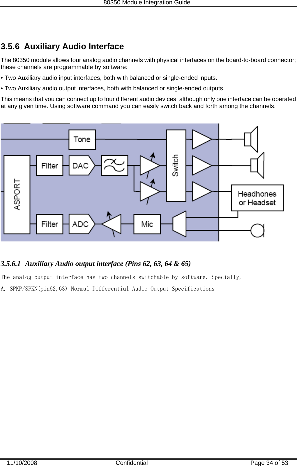
![80350 Module Integration Guide 11/10/2008 Confidential Page 50 of 53 References 1. AT Command Set Reference [80350 GSM/GPRS Modem Module AT Command Specification] 2. GSM 07.05: “Digital cellular telecommunications systems (Phase 2+); Use of Data Terminal Equipment – Data Circuit terminating Equipment (DTE – DCE) interface for Short Message Service (SMS) and Cell Broadcast Service (CBS)”. 3. GSM 07.07: “Digital cellular telecommunications systems (Phase 2+); AT command set for GSM Mobile Equipment (ME)”. 4. ITU-T Draft new Recommendation V.25ter: “Serial asynchronous automatic dialing and control”. 5. AD6720 Technical Data (REV. OCTOBER 18,2005) 6. NARROW-PITCH CONNECTORS Specifications (Jul.13, 2006) 7. U.FL-R-SMT (10) Specifications (Apr.17, 1997) 8. AK2301-MS0416-1-00 Specifications (Aug 31, 2005)](https://usermanual.wiki/Trimble/80350000A/User-Guide-1060416-Page-50.png)