Trimble 80350000A GSM/GPRS Modem Module User Manual 80350 Module rev1
Trimble Navigation Ltd GSM/GPRS Modem Module 80350 Module rev1
Trimble >
User manual

80350 Module Integration Guide
11/10/2008 Confidential Page 1 of 53
The 80350 Module
Integration Guide
Version 0.02
Cros Fan
Bing Xu
Chester Liu
Prepared by:
Dong-Ming Xia
Brian Pan
Yan-Jing Ji
Checked by:
Zheng-Bo Han
Approved by:

80350 Module Integration Guide
11/10/2008 Confidential Page 2 of 53
Contents
SAFETY INFORMATION................................................................................................................................................4
OVERVIEW........................................................................................................................................................................5
DOCUMENT HISTORY ...................................................................................................................................................5
REGULATORY COMPLIANCE FCC............................................................................................................................6
INTEGRATION CONSIDERATIONS AND INSTALLATION REQUIREMENTS ............................................................................6
DISCLAIMER ......................................................................................................................................................................6
1. INTRODUCTION.......................................................................................................................................................6
1.1 PRODUCT OVERVIEW............................................................................................................................................6
1.2 KEY FEATURES .....................................................................................................................................................6
1.3 PROVIDING MULTI-BAND OPERATION ..................................................................................................................6
1.4 SUMMARY OF FEATURES ......................................................................................................................................6
1.5 GENERAL DESIGN GUIDELINES ............................................................................................................................6
1.5.1 Advanced tips for an RF friendly layout ..................................................................................................6
1.5.2 Audio Reference Design ...........................................................................................................................6
2. TECHNICAL SPECIFICATION..............................................................................................................................6
2.1 BLOCK DIAGRAM ...................................................................................................................................................6
2.2 HARDWARE KEY PARTS........................................................................................................................................6
2.3 ABSOLUTE MAXIMUM RATINGS.............................................................................................................................6
3. PHYSICAL INTERFACES .......................................................................................................................................6
3.1 MODULE MOUNTING TO HOST BOARD (REFERENCE)..........................................................................................6
3.2 CONNECTORS .......................................................................................................................................................6
3.3 RF CONNECTION...................................................................................................................................................6
3.3.1 Coaxial Connector Option.........................................................................................................................6
3.3.2 Note: The above information regarding the connector and mating connector are taken from the pertinent
manufacturer specifications; for more details, please refer to the specifications of the part manufacturer.I/O
Connector
Pin
Assignment ...........................................................................................................................................6
3.3.2 I/O Connector
Pin
Assignment.....................................................................................................................6
3.4 ANTENNA...............................................................................................................................................................6
3.5 CONTROL CONNECTOR SIGNAL DESCRIPTIONS AND FUNCTIONS .......................................................................6
3.5.1 Module Power (Pins 41, 42, 43, 44 & 45)...............................................................................................6
3.5.2 Reset Signal (Pin 55).................................................................................................................................6
3.5.3 Power Control (pin 56)...............................................................................................................................6
3.5.4 SIM Interface (pins 16, 17,18 &19)..........................................................................................................6
3.5.5 PCM Interface (pins 23, 24, 25 & 26)......................................................................................................6
3.5.6 Auxiliary Audio Interface............................................................................................................................6
3.5.7 Serial Interface UART0..............................................................................................................................6
3.5.8 Debug communication(Pins 10, 31).........................................................................................................6
4. GSM/GPRS SERVICES.............................................................................................................................................6
4.1 TRANSMISSION MODES FOR THE GSM/GPRS SERVICES ..................................................................................6
4.2 VOICE COMMUNICATION .......................................................................................................................................6
4.3 CIRCUIT-SWITCHED DATA ....................................................................................................................................6
4.4 SHORT MESSAGE SERVICES(SMS).....................................................................................................................6
5. SIM OPERATION......................................................................................................................................................6
5.1 PROVISIONING THE SIM........................................................................................................................................6
5.2 GSM SUPPORTED SERVICES...............................................................................................................................6
5.3 GPRS SUPPORTED SERVICES.............................................................................................................................6

80350 Module Integration Guide
11/10/2008 Confidential Page 3 of 53
5.4 GSM MODES OF OPERATION...............................................................................................................................6
6. SOFTWARE INTERFACE .......................................................................................................................................6
6.1 API INTERFACE .....................................................................................................................................................6
6.2 AT COMMAND SET................................................................................................................................................6
7. SETUP AND INITIALIZATION..............................................................................................................................6
7.1 INITIALIZATION......................................................................................................................................................6
7.1.1 Start HyperTerminal...................................................................................................................................6
7.1.2 Initialization Command ..............................................................................................................................6
7.2 SEND SMS EXAMPLE ...........................................................................................................................................6
7.3 VOICE CALL EXAMPLE ..........................................................................................................................................6
7.3.1 MO ................................................................................................................................................................6
7.3.2 MT.................................................................................................................................................................6
7.4 GPRS PACKET EXAMPLES...................................................................................................................................6
REFERENCES....................................................................................................................................................................6
ABBREVIATION ...............................................................................................................................................................6

80350 Module Integration Guide
11/10/2008 Confidential Page 4 of 53
Safety Precautions
Before you use the 80350 module, please carefully read this section to understand the correct method of use
and ensure the safety of the holder, others and properties.
z Do not expose the 80350 module to open flames.
z Ensure that liquids do not spill onto the 80350 module.
z Do not use the 80350 module in an environment of extremely high or low temperature, otherwise,
malfunctions may be caused.
z Using the 80350 module in an environment of moist or high humidity may cause malfunctions of the
product.
z Do not drop or strongly impact the 80350 module; otherwise, malfunctions may be caused and the
product cannot be used.
z Do not use the 80350 module near any electronic device vulnerable to interference. Otherwise,
malfunctions of electronic device may result. Such electronic devices include medical electronic devices,
such as hearing aids and pacemaker, fire alarms, auto doors and other automatic equipment. If you
have to use the 80350 module near such devices, please first consult the manufacturers and dealers of
these devices to avoid interference.
z Do not dispose the 80350 module as urban waste. For details, please refer to the local regulations for
proper disposal of waste electronics.
z Do not attempt to disassemble the 80350 module; doing so will void the warranty. With the exception of
the Subscriber Identification Module (SIM), this product does not contain consumer-serviceable
components.
z The specifications of this product are subject to change due to improvement of its functionality without
notice.

80350 Module Integration Guide
11/10/2008 Confidential Page 5 of 53
Overview
This document is intended to offer the application developer a reference to the 80350 module’s hardware and
software specifications and interfaces.
Document History
Version Date Author Comments
0.00 09/05/2008 PPD Draft
0.01 10/29/2008 PPD Revised per TNL’s comments and other
comments
0.02 11/25/2008 PPD FCC/IC/CE compliance declaration
wording revised

80350 Module Integration Guide
11/10/2008 Confidential Page 6 of 53
Regulatory Compliance
Declaration of Conformity
This device meets the FCC Radiofrequency Emission Guidelines and is certified with the FCC as:
Model number: 80350
FCC ID number: JUP80350000A.
Industry Canada ID number: 1756A-8035000A
Identification mark: 1588 (Notified Body) CE.
Person responsible for making this declaration: Brian Jackson, Trimble Navigation Ltd., 935 Steward Dr.,
Sunnyvale, CA 94085, USA.
Compliance with CE Rules and Regulations
For compliance purposes, the label must show the CE Mark and Notified Body number. The product must be
correctly installed in order to maintain compliance.. The RF safety has been based on an MPE calculation;
therefore, the device must be used at more than 20 cm (or 7.9 in.) from the body. Also, the compliance of the
host product (containing the module) is the responsibility of the integrator who puts the host product on the
market, and further testing may be required, with this module installed in the host device.
Compliance with FCC/IC Rules and Regulations
This device complies with part 15 of the FCC Rules. Operation is subject to the condition that this device does
not cause harmful interference, and that this device must accept any interference received, including
interference that may cause undesired operation.
Caution
Changes or modifications not expressly approved by the manufacturer could void the user’s authority to operate
the equipment.
When incorporating the 80350 module in a host product, the integrator must ensure that the host product
comply with relevant FCC requirements and regulations.
For mobile or fixed applications (with the device at least 20 cm or 7.9 in. distance from the body), the integrator
is authorized to use the FCC/IC Grants and Certificates of this module for their host product if the module is
integrated and installed in accordance with the conditions under which the module has been tested and
certified. In this case the FCC label of the module shall be visible from the outside, or the host product shall bear
a label making reference to the module inside (the label should state “Contains FCC ID JUP80350000A” or
something to the effect). FCC RF safety regulations require a warning label prompting the user to keep the
antenna of a device in operation at least 20 cm or 7.9 in. distance from the body.

80350 Module Integration Guide
11/10/2008 Confidential Page 7 of 53
Important
For portable applications (with the device less than 20 cm or 7.9 in. distance from the body), the integrator are
required to have their host product certified to obtain its own FCC/IC Grants and Certificates. This is mandatory
to meet the SAR requirements for portable wireless devices. See www.fcc.gov/oet/rfsafety for more information
on RF exposure safety and product labeling requirements.
Disclaimer
The 80350 module and the information and statement in this document, at the time of its publication, are in
compliance with FCC, PTCRB, IC and CE rules and regulations. Liability from any usage that violates these
rules and regulations is the sole responsibility of the user.
It is strongly recommended that the installation and tuning of the 80350 module be only undertaken by RF
specialists with adequate experience and credentials. The reference design and suggested methods for
installing and tuning the module shall not be deemed applicable under all possible environments and conditions
of application; the manufacturer shall not be held liable for incorrect parameters or measurements as a result of
egression from the range of environments and conditions considered by the manufacturer.
The manufacturer shall not be held responsible for bodily injuries or property damages as a result of installing
and using the 80350 module.

80350 Module Integration Guide
11/10/2008 Confidential Page 8 of 53
1. Introduction
1.1 Product Overview
The 80350 module is a highly integrated GSM/GPRS module, which has built-in support for RF, voice, power
management, among other functionalities, and is in compliance with GSM/GPRS wireless communication
standards.
1.2 Key Features
The following table summarizes the main features of the 80350 module.
Data input/output interface 80-pin connector
Primary serial port full 9-pin, UART implementation
PCM Port Only support salve (only for Audio PCM)
Voice Support 2 Audio In and 2 Audio out
Antenna Interface Ultra-miniature coaxial connector
Command protocol GSM AT command set (80350 GSM/GPRS Modem Module
AT Command Specification)
Interface
Subscriber Identification
Module (SIM) Optional 1.8/3 V mini-SIM carrier and interface on-board with
SIM detect
Electrical power 3.55V to 4.2V (VBATT) Power
Peak currents and average
power dissipation Refer to the Operating Power table in the summary of features
for peak currents and average power dissipation for various
modes of operation.
Frequency bands EGSM 900, GSM1800, GSM 850 and GSM 1900 capability. Radio
Features GSM/GPRS features
supported Provides for all GSM/GPRS authentication, encryption, and
frequency hopping algorithms. GPRS Coding Schemes
CS1-CS4 supported. Multi-Slot Class 10 (4RX/2TX, Max 5
Slots)
Regulatory Agency approvals • GCF Type Approval
• PTCRB Type Approval
• FCC Certification
• CE (Conformité Européenne)
• IC (Industry Canada) Approval
80350 Module Integration Guide
11/10/2008 Confidential Page 9 of 53
GSM/GPRS
Functionality • Mobile-originated and mobile-terminated SMS messages: up to 140 bytes or up to 160 GSM
7-bit ASCII characters.
• Reception of Cell Broadcast Messages
• SMS Receipt acknowledgement
• Circuit Switched Data (Transparent & Non-transparent up to 9.6 Kbps)
• Voice (EFR, FR, HR, and AMR)
• Supports Unstructured Supplementary Service Data (USSD)
• Multi-Slot Class 10 Supported (4Rx/2TX, 5 Slot Max)
• PBCCH/PCCCH supported
Audio
Features • Microphone biasing
• 2 Analog Audio Input
• 2 Analog Audio Output
SIM 1.8/3 V Mini-Subscriber Identity Module (SIM) compatible
1.3 Providing Multi-Band Operation
The 80350 module supports quad-band GSM operation: 850/900/1800/1900MHz.
1.4 Summary of Features
Mechanical:
Dimensions 45.7 mm x 34.1 mm x 3.5 mm (not including mounting tabs)
Weight 8.1 g
Packet Data Transfer:
Protocol GPRS Release 97
Coding Schemes CS1-CS4
Multi-Slot Capability: (Demonstrated @MS10) MS10 (4RX/2TX, Max 5 Slots)
Packet Channel Support PBCCH/PCCCH
Circuit Switched Data Transfer:
V110 300 bps/1200 bps/2400 bps/4800 bps/9600 bps/14,400 bps
Non-Transparent 300 bps/1200 bps/2400 bps/4800 bps/9600 bps/14,400 bps
Short Message Services:
GSM SMS MO, MT, CB, Text and PDU Modes
GPRS SMS MO, MT, CB, Text and PDU Mode
Voice Capability:
Speech Codec EFR, FR, HR, and AMR
GSM/GPRS Radio Performance Multi-Band:
Radio Frequencies 850 MHz, 900 MHz, 1800 MHz and 1900 MHz
Sensitivity <-102 dBm (Typical GPRS CS1)
850 & 900 MHz Transmit Power Class 4 (2 W)
1800 & 1900 MHz Transmit Power Class 1 (1 W)
System Requirements:
Host Interface Serial Interface
DC Voltage 3.55 to 4.2 V
80350 Module Integration Guide
11/10/2008 Confidential Page 10 of 53
Application Interface:
Host Protocol AT Commands
Internal Protocols UDP stack, TCP/IP stack, PPP, PAD and CMUX
Physical Interface 1 serial (primary) and I2C
Audio Interface • Microphone biasing
• 2 Analog Audio Input
• 2 Analog Audio Output
SIM Interface:
Remote SIM Option 1.8/3-Volt SIM Capability
Environmental:
Compliant Operating Temp -20 °C to 60 °C (Fully GSM Spec Compliant)
Operating Temperature -20 °C to 70 °C
Storage Temperature -40 °C to 85 °C
Humidity 5 to 95% non-condensing
EMC:
Emissions FCC Parts 15 Class B & 22 & 24, IC & CE
Operating Power (Typical):
GSM Operation
GSM 850/900 (1 RX/1 TX, full power) 66 mA min, 221 mA average, 1.23 A peak
GSM 1800 (1 RX/1 TX, full power) 59 mA min,170 mA average, 775 mA peak
GSM 1900 (1 RX/1 TX, full power) 58 mA min,161 mA average, 711mA peak
Idle <5 mA Average
Shutdown <1mA
GPRS Operation Power
EGSM 850/900 (4 RX/1 TX, full power) 146 mA min, 247 mA average, 1.28 A peak
EGSM 850/900 (2 RX/2 TX, full power) 71 mA min, 370 mA average, 1.28 A peak
GSM 1800 (4 RX/1 TX, full power) 159mA min, 193 mA average, 796 mA peak
GSM 1800 (2 RX/2 TX, full power) 112 mA min, 259 mA average,786 mA peak
GSM 1900 (4 RX/1 TX, full power) 154 mA min, 185 mA average, 751mA peak
GSM 1900 (2 RX/2 TX, full power) 60 mA min, 246 mA average, 736mA peak
Idle <5 mA average
Shutdown <1mA
GSM Transmit Power:
1800/1900 MHz GSM Power Class 1 (30 dBm ± 2 dB @ antenna connection
850/900 MHz GSM Power Class 4 (33 dBm ± 2 dB @ antenna connection)
GSM/GPRS Receiver Sensitivity (Typical):
1800/1900 MHz <-102 dBm, GPRS Coding Scheme 1 (CS1)
850/900 MHz <-102 dBm, GPRS Coding Scheme 1 (CS1)
80350 Module Integration Guide
11/10/2008 Confidential Page 11 of 53
1.5 General Design Guidelines
1.5.1 Advanced tips for an RF friendly layout
1.5.1.1 Ground Plane
When designing the 80350 module into the host application, special care must be taken regarding the design of
grounding on the host PCB. Proper grounding of the module’ is an essential part of any good application, as it
can very effectively keep EMI in check and ensure good heat dissipation. An example is shown in the drawing
below:
1. It is recommended that the entire board space underneath the 80350 module be made the ground plate
with sufficient ground vias, and this ground be adequately connected to the mounting tab ground. In doing
so, good connectivity can be achieved between the module’s ground and that of the host board.
2. Running traces beneath this ground plate is strongly discouraged.
80350 Module Integration Guide
11/10/2008 Confidential Page 12 of 53
1.5.1.2 Antenna and RF Signal Trace
For best antenna performance, please ensure that the antenna’s RF trace be designed to be 50 ohm special
impedance line, and that there are a sufficient number of ground holes around the antenna impedance line and
connector. Keep other traces of the module and the host board as far from this impedance line as possible. It
should be avoided that other traces run in parallel to or cross the antenna impedance line. The antenna should
be kept away metallic components.
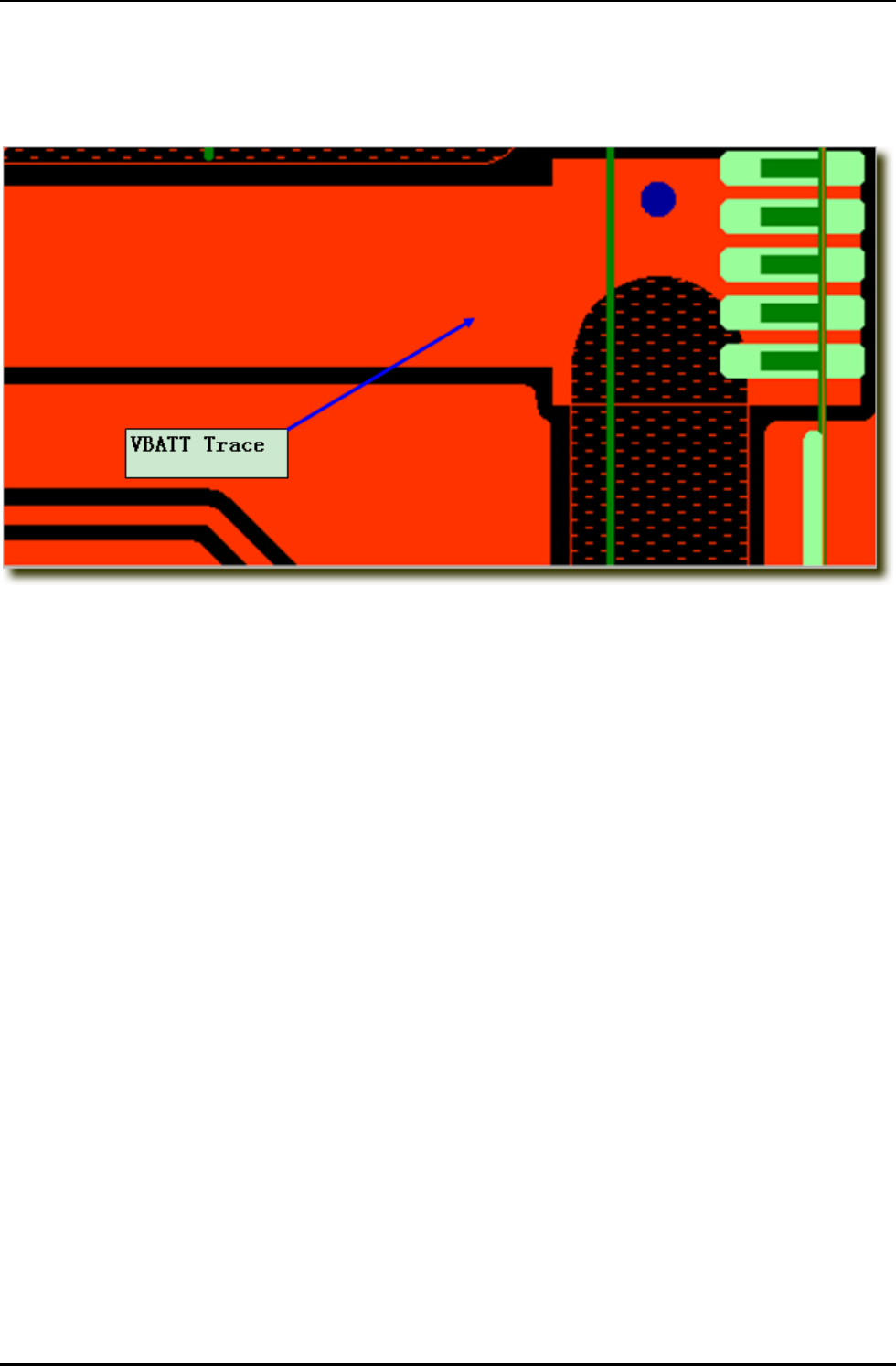
1.5.1.3 Vbatt Input
The power supply of the 80350 module is of critical importance to the module’s stability and safety. The 80350
module encompasses all working elements of GSM. It is recommended that the width of power trace be greater
than 2 mm, and that a sufficiently large capacitor be placed in the nearest vicinity of the Power pin (two 1000uF
capacitors, preferably, low ESR Tantalum capacitors) in order to cope with bursts during GSM operation (such
bursts cause voltage transients as shown in the figure below).
80350 Module Integration Guide
11/10/2008 Confidential Page 13 of 53
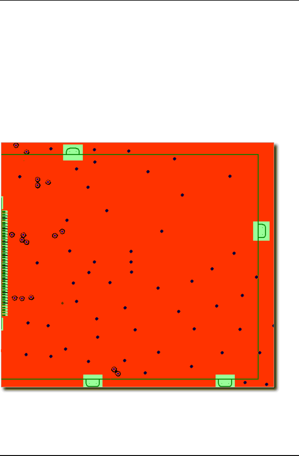
The following picture shows an example of the power supply trace for the module. The trace covers the entire
power pin of the module. The wide trace is intended to minimize voltage drop over the trace.
.
80350 Module Integration Guide
11/10/2008 Confidential Page 14 of 53
1.5.2 Audio Reference Design
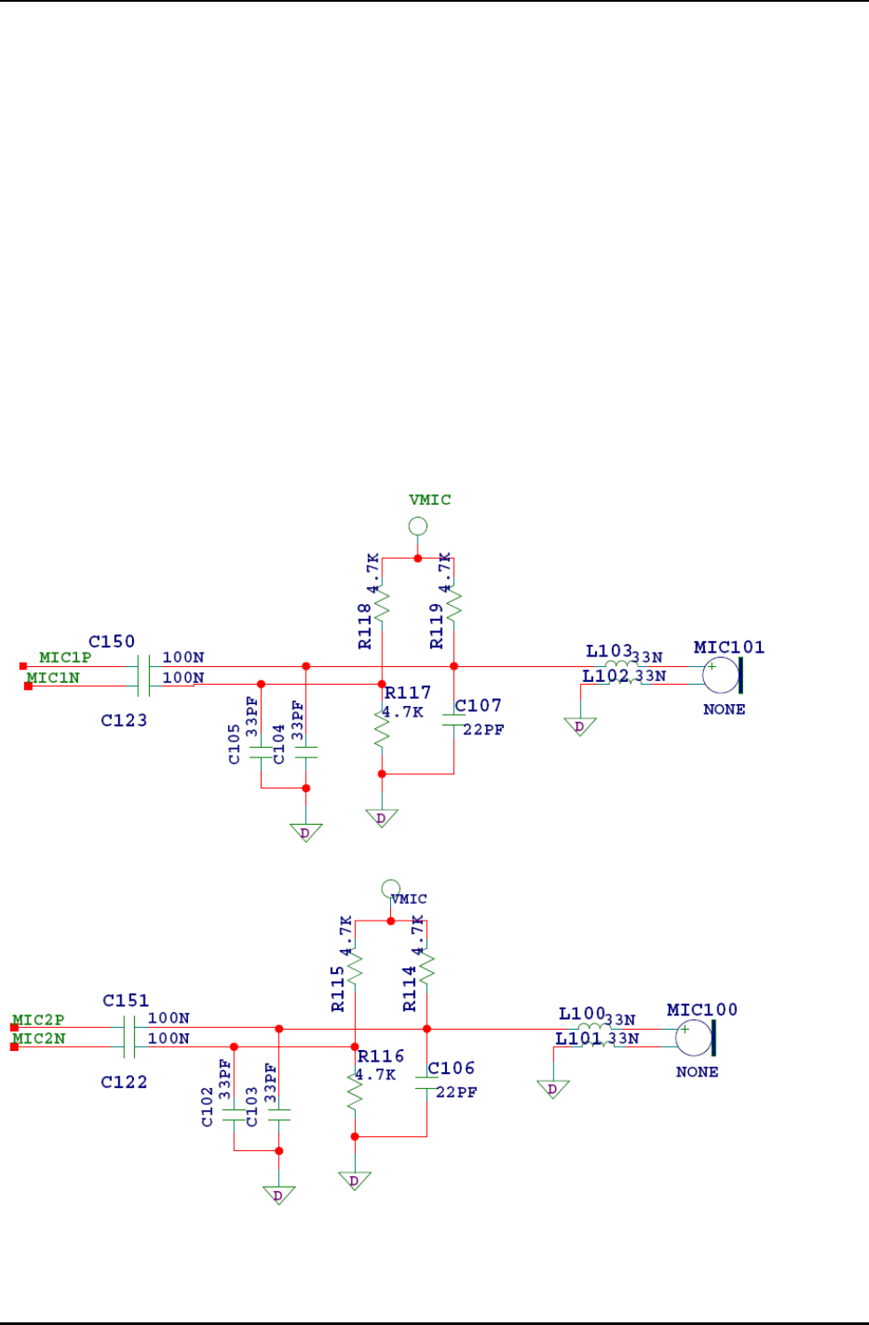
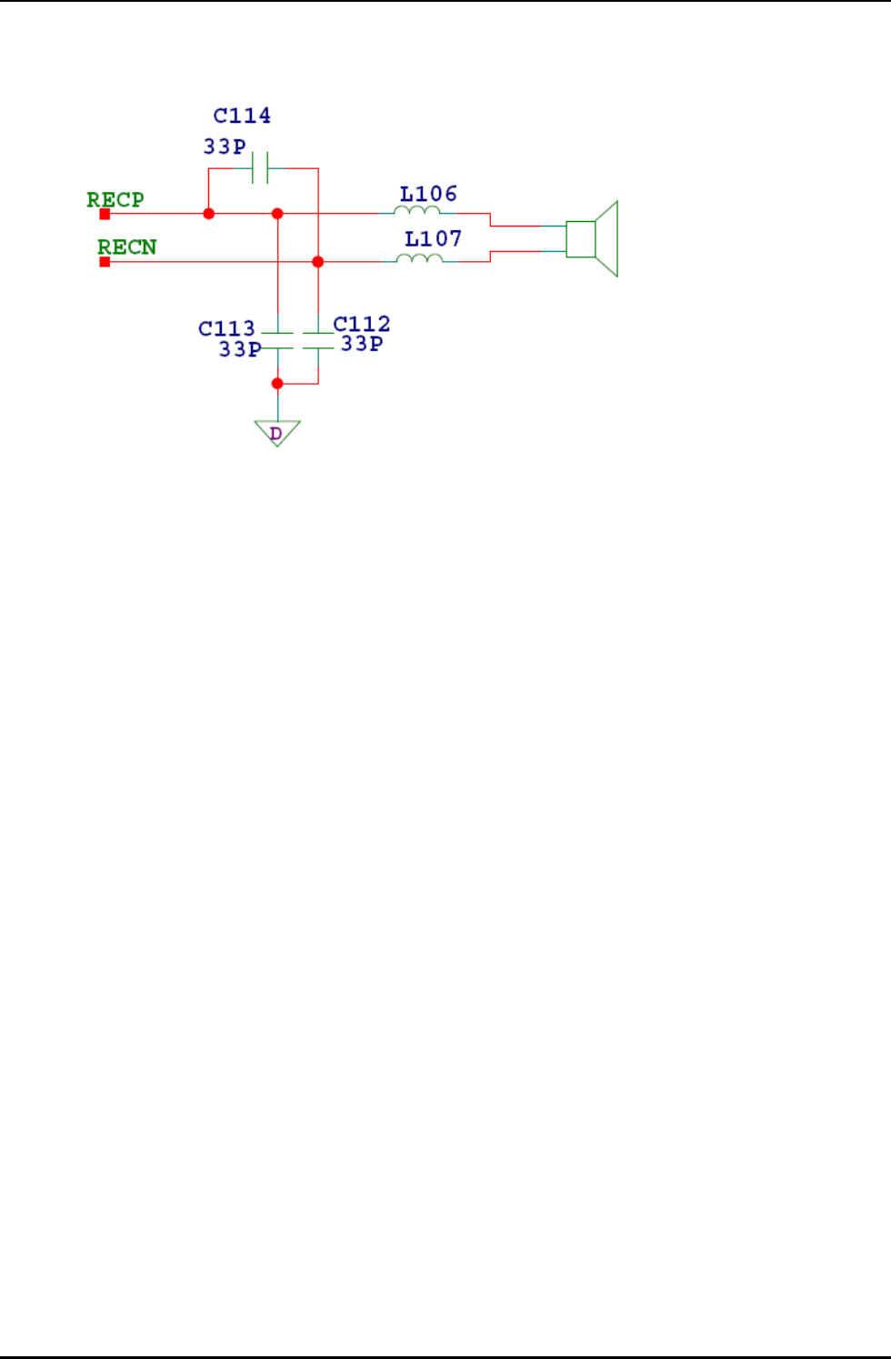
1.5.2.1 Audio schematics
The audio quality is very much dependent on the circuit design and layout. As an aid to obtaining good audio
quality, a reference design has been included below.
1. Please serially place a Bead on Audio In/Out (see in the following circuit: L100, L101, L102, L103, L106 and
L107) in order to reduce GSM TDD noise. Bead (100MHz, R>=1K ohm) is recommended.
2. Add a small capacitor on each audio trace. This small capacitor is for further reducing the TDD noise. The
typical value of capacitance is 10pF to 100pF. The actually value needs to be tuned based on the location
and layout of the audio circuitry.
3. The suggested locations of the capacitors and Bead are in the vicinity of Microphone and Receiver, rather
than the module.
4. Maintain proper separation of the Audio In reference ground from the Audio Out reference ground so as to
minimize ECHO coupling in the circuitry.
5. Microphone and Receiver should be physically separated from one another, e.g., on the two far ends of the
evaluation board, as the spatial coupling of voice signal may occur, resulting in ECHO or screeching sound.
80350 Module Integration Guide
11/10/2008 Confidential Page 15 of 53
1.5.2.2 Audio Layout
Audio signals are very weak and are in the category of weak analog signals; they are extremely susceptible to
interference from digital signals. Therefore, it is suggested that audio signal traces follow the same layer
differential trace layout method, and be kept far away from strong digital signals (e.g., power signal, RF related
signal, CLK signal and high-speed Bus).
80350 Module Integration Guide
11/10/2008 Confidential Page 16 of 53
2. Technical Specification
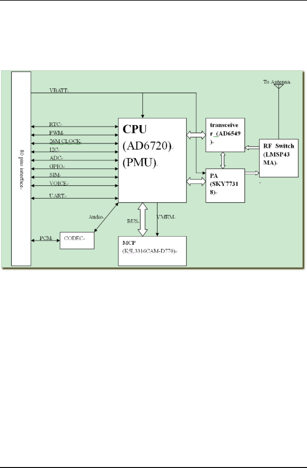
2.1 Block Diagram
80350 Module Integration Guide
11/10/2008 Confidential Page 17 of 53
2.2 Hardware Key Parts
Part Description
CPU IC-CPU,AD6720ABCZ-RL,GP,BGA,TAP,39MHZ,289PIN,ADI
Memory IC-MEMORY,K5L3316CAM-D770,GP,FBGA,TRAY,SAMSUNG
Transceiver IC-RF,AD6549BCPZ,GP,LFCSP,TAP,32PIN,GSM850/900 DCS/PCS,ADI
RF Switcher IC-RFSW,LMSP43MA-271TEMP,GP,QFN,TAP,16PIN,GSM,MURATA
SAW-Filter FILTER,SAFED881MFL0F05R00,GP,881.5MHZ,5P,MURATA
SAW-Filter FILTER,SAFED1G96FA0F00R00-GP,GP,1.96GHZ,5P,MURATA
SAW-Filter FILTER,SAFED942MFM0F00R00-GP,GP,942.5MHZ,5P,MURATA
SAW-Filter FILTER,SAFED1G84FB0F00R00-GP,GP,1842.5MHZ,5P,MURATA
Oscillator XTAL,MC-146,GP,32.768KHZ,20PPM,12.5PF,EPS
TCXO XTAL,TTS18VSG-A5,GP,26MHZ,10PPM,3.5PF,TOKYO
RF-PA IC-RF,SKY77318,GP,TAP,20PIN,GSM900/GSM850,SKYWORKS
B2B Connector CONN,AXK880125WG,GP,80PIN,SMD,TAP,FPC,MA
RF Connector CONN,CL331-0471-0-10,GP,ML,2PIN,SMD,TAP,HRS
2.3 Absolute Maximum Ratings
The absolute maximum ratings stated in following Table are stress ratings under any conditions. Stresses
beyond any of these limits will cause permanent damage to the 80350 module.
Parameter Min Max Unit
Supply Voltage BATT -0.3 5.5 V
Voltage at digital pins in POWER DOWN mode -0.3 0.3 V
Voltage at digital pins in normal operation -0.3 3.05 or
VEXT+0.3 V
Voltage at analog pins in POWER DOWN mode -0.3 0.3 V
Voltage at VCHARGE pin -0.3 5.5 V
VSENSE 5.5 V
ISENSE 5.5 V
VRTC -0.3 5.5 V
Operating Rating: -20°C to +70°C
Storage Temperatures: -40°C to +85°C
80350 Module Integration Guide
11/10/2008 Confidential Page 18 of 53
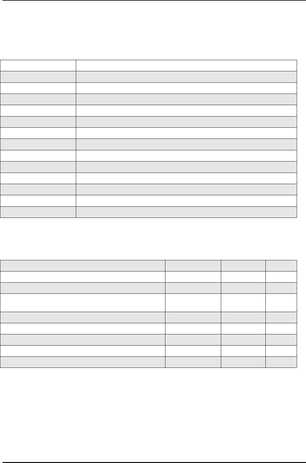
3. Physical Interfaces
Mounting Tabs
80350 Dimension (mm)
80350 Module Integration Guide
11/10/2008 Confidential Page 19 of 53
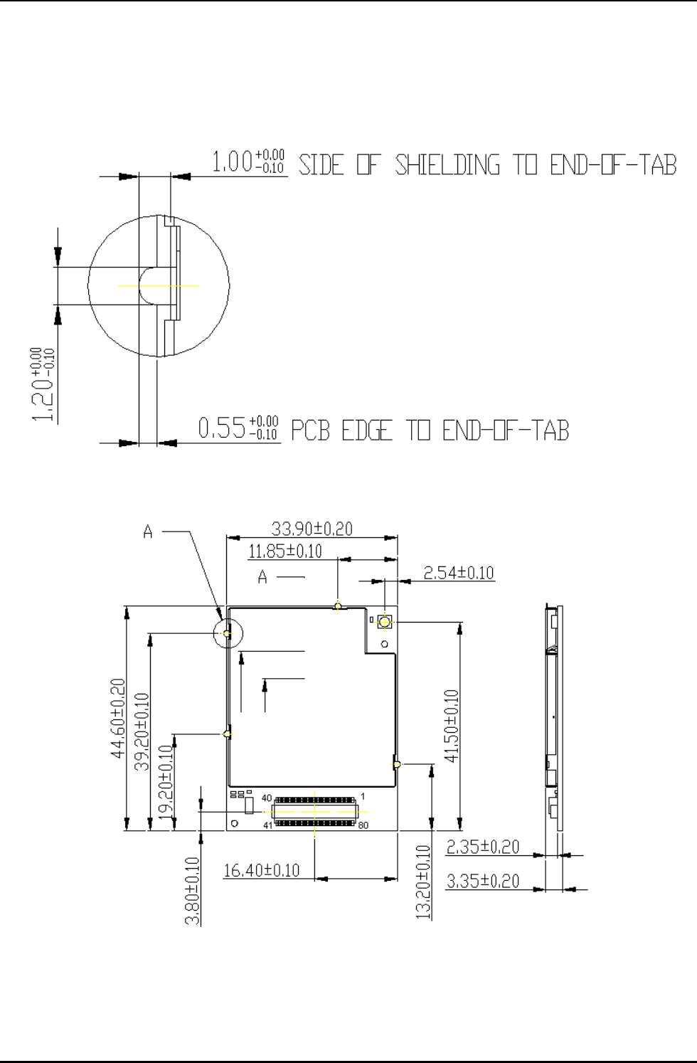
3.1 Module Mounting to Host Board (Reference)
The module provides mounting tabs that needs to be soldered to a PCB. These tabs provide circuit grounding
for the module.
Host Board Layout
80350 Module Integration Guide
11/10/2008 Confidential Page 20 of 53
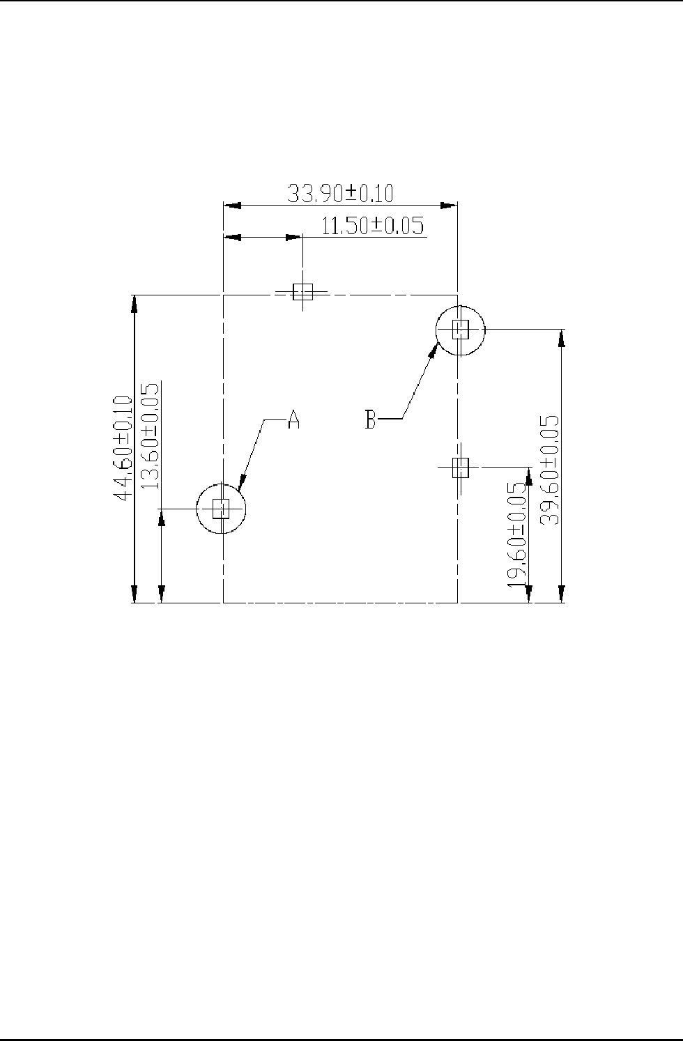
A Type Pad
B Type Pad
80350 Module Integration Guide
11/10/2008 Confidential Page 21 of 53
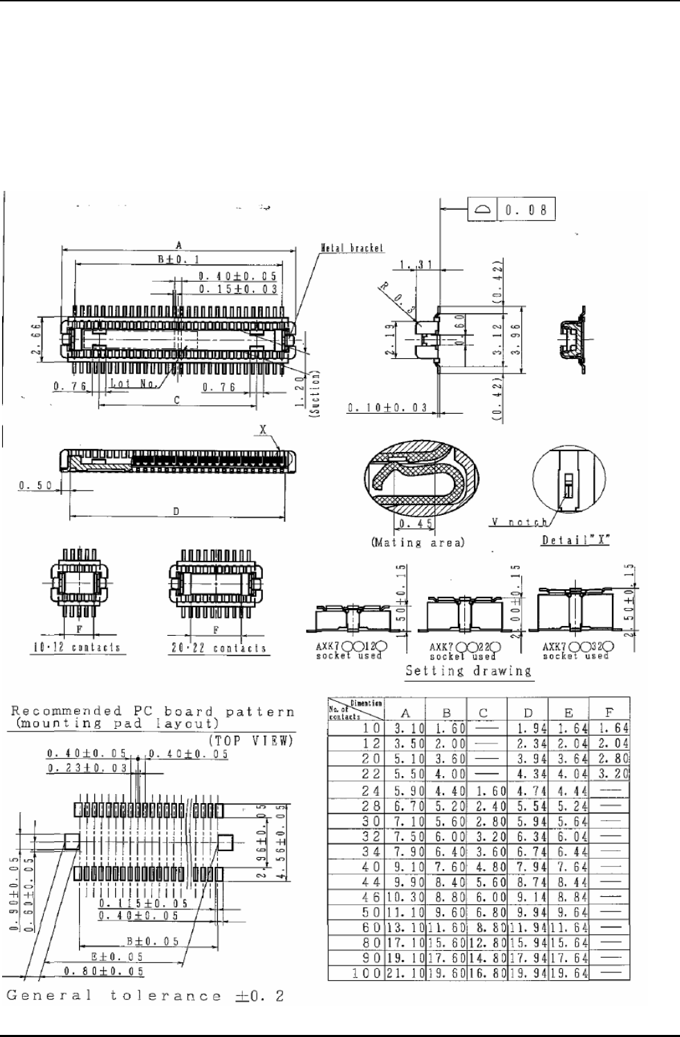
3.2 Connectors
On the 80350 module: CONN,AXK880125WG,GP,80PIN,SMD,TAP,FPC,MAT
Modem module manufacturer Part Number is 6012A0190101.
MATSUSHITA Part Number is AXK880125WG
80350 Module Integration Guide
11/10/2008 Confidential Page 22 of 53
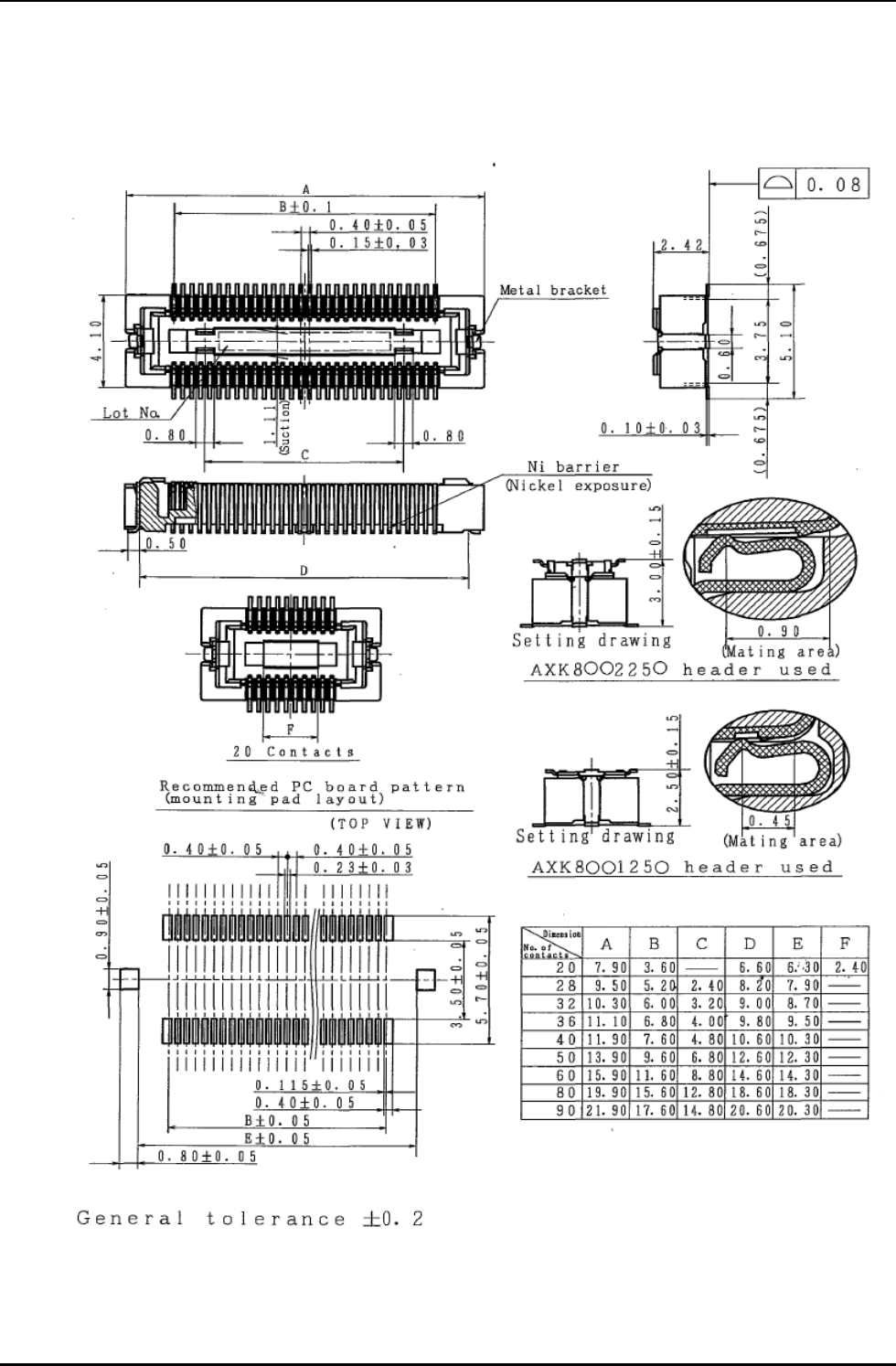
On the Host: CONN,AXK780327G,GP,x,80PIN,SMD,TAP,FPC,MAT
Modem module manufacturer Part Number = 6012A0190001
MATSUSHITA Part Number is AXK780327G
Note: The above information regarding the connector and mating connector are taken from the pertinent manufacturer
specifications; for more details, please refer to the specifications of the part manufacturer
80350 Module Integration Guide
11/10/2008 Confidential Page 23 of 53
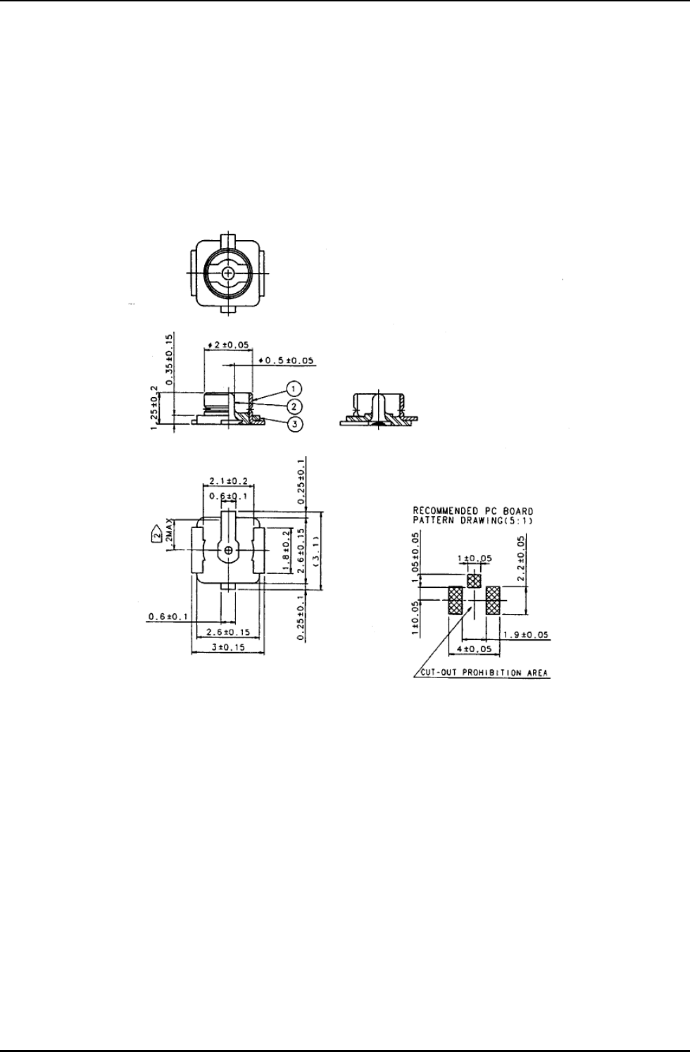
3.3 RF Connection
3.3.1 Coaxial Connector Option
On the module: GP,ML,2PIN,SMD,TAP
Internal Part Number = 6012A0189501
HIROSE: CL331-0471-0-10
3.3.2 Note: The above information regarding the connector and mating
connector are taken from the pertinent manufacturer specifications; for more
details, please refer to the specifications of the part manufacturer.

80350 Module Integration Guide
11/10/2008 Confidential Page 24 of 53
I/O Connector Pin Assignment
The following table shows the pin assignment on the input/output connector.
Pin I/O 80350 Define Description (Default function / secondary function)
1 Ground DGND Ground
2 Reserved Floating
3 NC No connect
4 Ground DGND Ground
5 Reserved Floating
6 Reserved Floating
7 Reserved Floating
8 Reserved Floating
9 Reserved Floating
10 DBGTX Debug TX
11 Reserved Floating
12 NC No connect
13 NC No connect
14 Reserved Floating
15 NC No connect
16 SIM_CLK SIM interface clock
17 SIM_VCC SIM interface vcc
18 SIM_DAT SIM interface data
19 SIM_RST SIM interface reset
20 NC No connect
21 NC No connect
22 NC No connect
23 PCM_CLK PCM interface clock
24 PCM_SYNC PCM interface sync
25 PCM_RXD PCM interface RXD
26 PCM_TXD PCM interface TXD
27 Reserved Floating
28 Reserved Floating
29 Reserved Floating
30 UART RXD0 Serial data input
31 UART DBGRX Debug RXD
32 UART TXD0 Serial data output
33 Reserved Floating
34 Reserved Floating
35 Reserved Floating
36 Ground DGND Ground
37 Ground DGND Ground
38 Ground DGND Ground
39 Ground DGND Ground
40 Ground DGND Ground
41 Power VBATT Power
42 Power VBATT Power
43 Power VBATT Power
44 Power VBATT Power
45 Power VBATT Power

80350 Module Integration Guide
11/10/2008 Confidential Page 25 of 53
46 Reserved Floating
47 UART RING0 ring indicate
48 UART DSR0 Data set ready
49 UART RTS0 Ready to send
50 UART DTR0 Data terminal ready0
51 Reserved Floating
52 UART CTS0 Clear to Send
53 Reserved Floating
54 UART DCD0 Data carrier detect
55 I /RESET External Reset input
56 O POWER_KEY Power Key
57 Ground AGND Ground
58 Analog MIC1N Auxiliary Audio input
59 Analog MIC1P Auxiliary Audio input
60 Analog MIC2P Auxiliary Audio input
61 Analog MIC2N Auxiliary Audio input
62 Analog SPKN Auxiliary Audio output
63 Analog SPKP Auxiliary Audio output
64 Analog RECP Auxiliary Audio output
65 Analog RECN Auxiliary Audio output
66 Reserved Floating
67 Power Reserved Floating
68 NC No connect
69 NC No connect
70 Reserved Floating
71 NC No connect
72 NC No connect
73 NC No connect
74 Reserved Floating
75 Reserved Floating
76 Reserved Floating
77 NC No connect
78 Reserved Floating
79 NC No connect
80 Ground DGND Ground
I = Input;
O = Output;
NC = No connect
3.4 Antenna
The 80350 module has an RF antenna interface; for its specification, please refer to Section 3.3.1. Note that this
RF connector is a connector only, and is not a switch. Through this connector, various RF performance
parameters of the module can be measured.
80350 Module Integration Guide
11/10/2008 Confidential Page 26 of 53
3.5 Control Connector Signal Descriptions and Functions
3.5.1 Module Power (Pins 41, 42, 43, 44 & 45)
The 80350 module requires a single power supply and no additional working power supply is required. The
relevant parameters are defined in the following table.
The module has multiple LDOs (Low Drop Linear Voltage Regulators) inside, which support various different
working units, including internal memory, GSM RF, CPU, IO ports, audio, etc. Therefore, the 80350 module
depends heavily on external power supply, which directly impacts, the stability and RF performance parameters
of the module. Please carefully follow the description of power supply and ground in Sections 1.5.1 and 1.5.3.
The 80350 module uses a single voltage source of VBATT = +3.55V to 4.2V.
VBATT Parameters/Conditions Min. Typ. Max. Units
Main Battery Supply Voltage In Regulation 3.55 3.8 4.2 Vdc
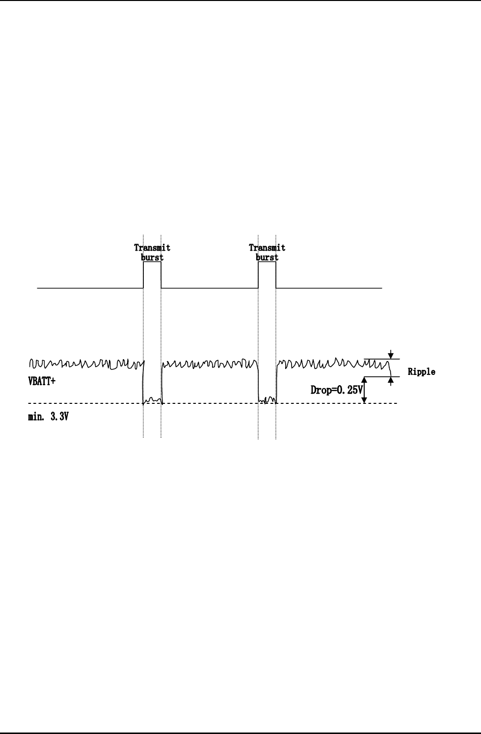
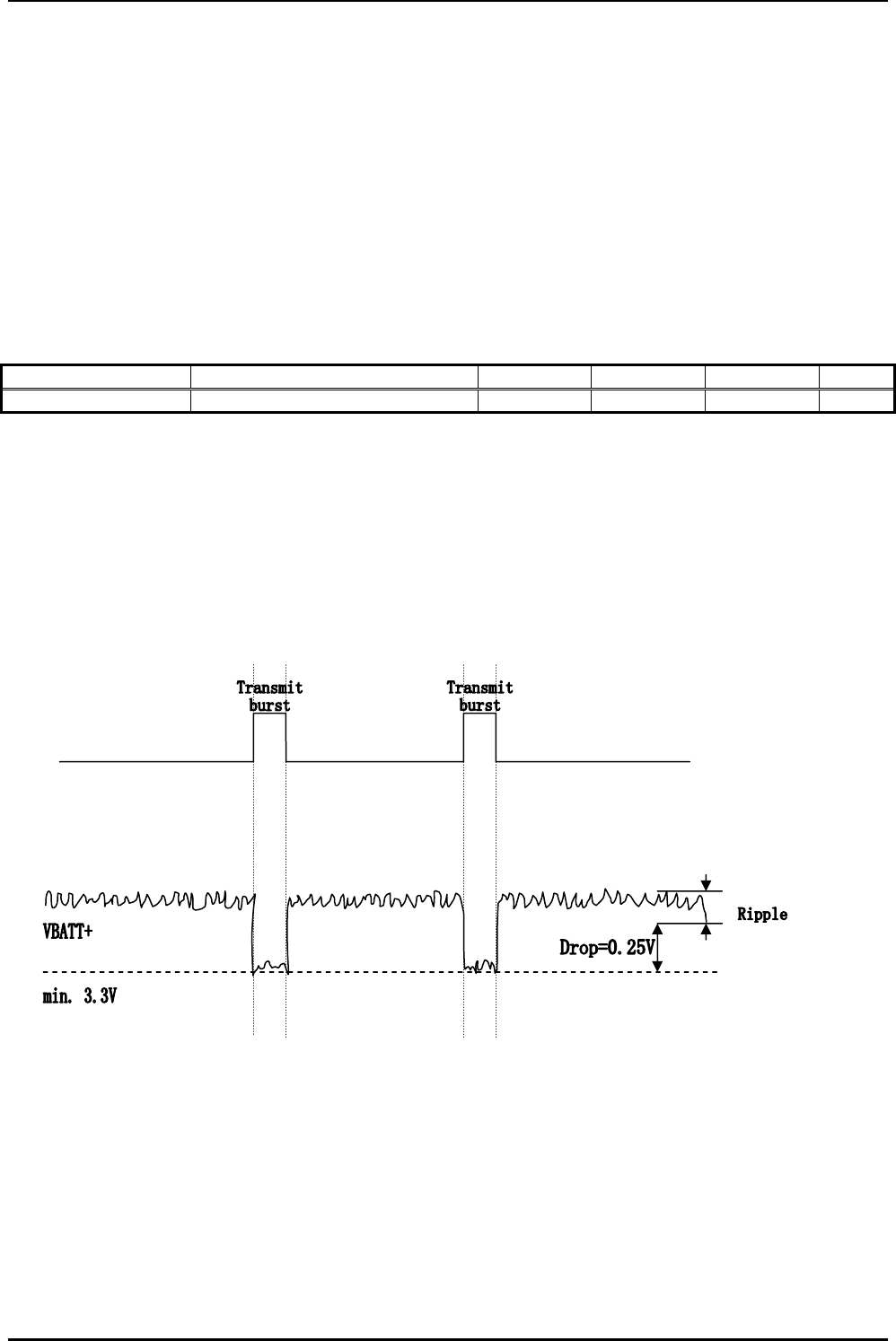
Minimizing Power Loss
The measurement network monitors outburst and inburst values. The drop is the difference of both
values. The maximum drop (Dmax) since the last start of the module will be saved. In IDLE and
SLEEP mode, the module switches off if the minimum battery voltage (Vbattmin) is reached.
Example:
VImin = 3.3V
Dmax = 0.25 V
Vbattmin = VImin + Dmax
Vbattmin = 3.3V + 0.25V = 3.55V
For Example:
Figure : Power supply limits during transmit burst
3.5.2 Reset Signal (Pin 55)
The Reset signal is an input to the 80350 module. It is used to reset the module during emergency situations;
the signal is Low active..
80350 Module Integration Guide
11/10/2008 Confidential Page 27 of 53
When the module is running in a undefined or uncontrollable state, it can be reset by forcefully pulling Low the
RESET signal port. It should be noted that all pending processes will be aborted, and hence, will need to be
restarted.
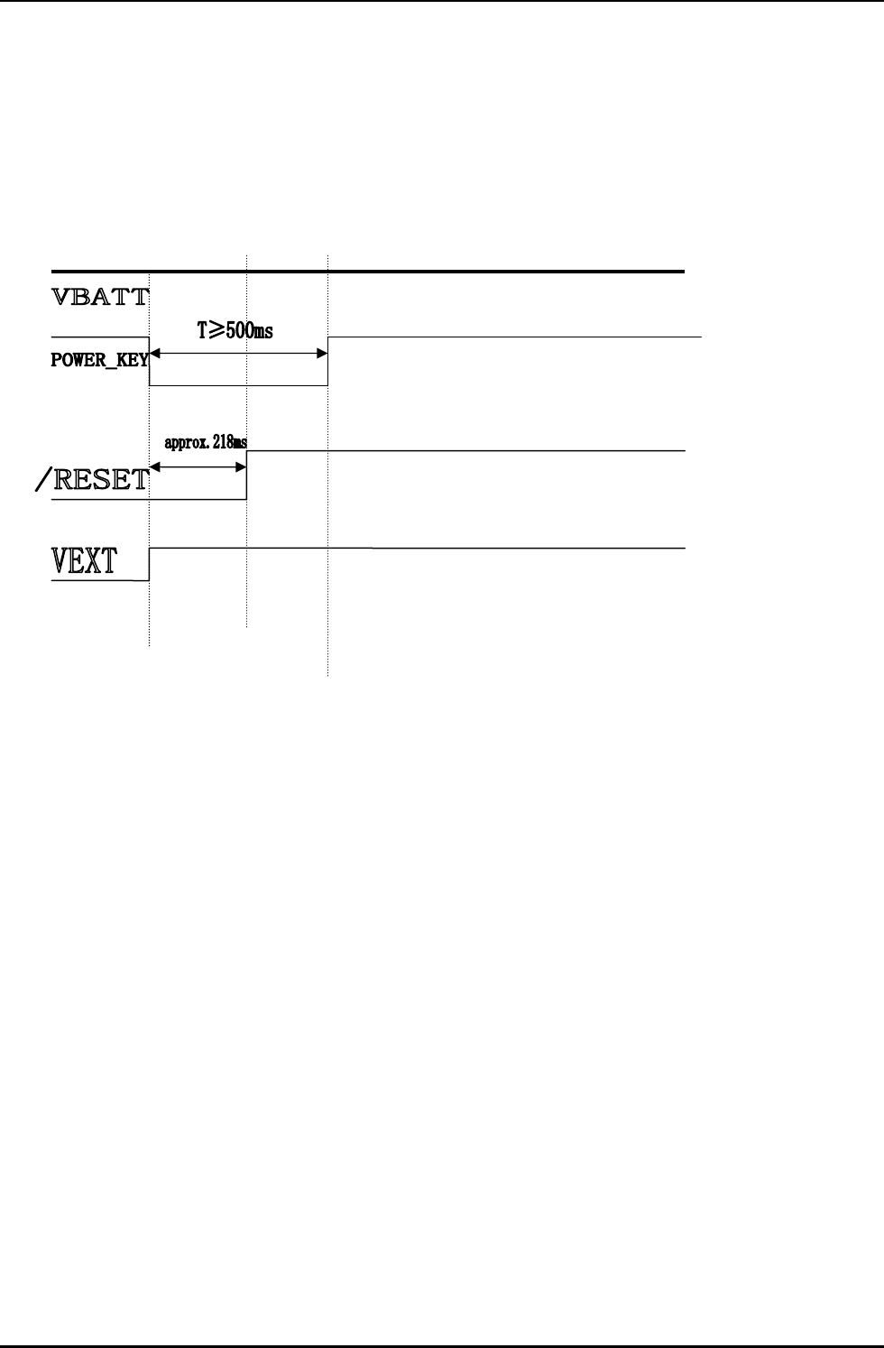
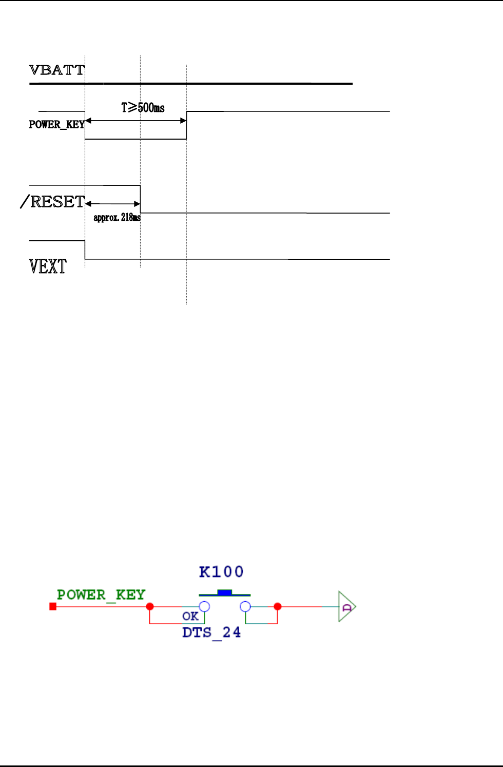
Note: During normal module operation, please do not operate on the RESET signal pin. The following diagram
shows the relevant signal timings in the module during its Power-On/Power-Off
Power-On / Power-Off and RESET Scenarios
Figure : Power-on and reset with operating voltage at VBATT
80350 Module Integration Guide
11/10/2008 Confidential Page 28 of 53
Figure : Power-Off and RESET with operating voltage at VBATT
3.5.3 Power Control (pin 56)
The input is equivalent to a “phone ON-button”. A falling-edge on this Active-Low input will switch-ON the
module or switch-OFF the module after a delay.
Please see the “Power-On / Power-Off and RESET Scenarios”
3.5.3.1 Power On
Pulling the POWER_KEY line on the module LOW for at least 500 msec (after Vbatt is applied and stabilized) is
required to turn it ON.
3.5.3.2 Power Off
The module can be turned off by a low pulse on the POWER_KEY pin.
3.5.3.3 Using the Power Control Signal
Typical use powering module on/off with a switch:
80350 Module Integration Guide
11/10/2008 Confidential Page 29 of 53
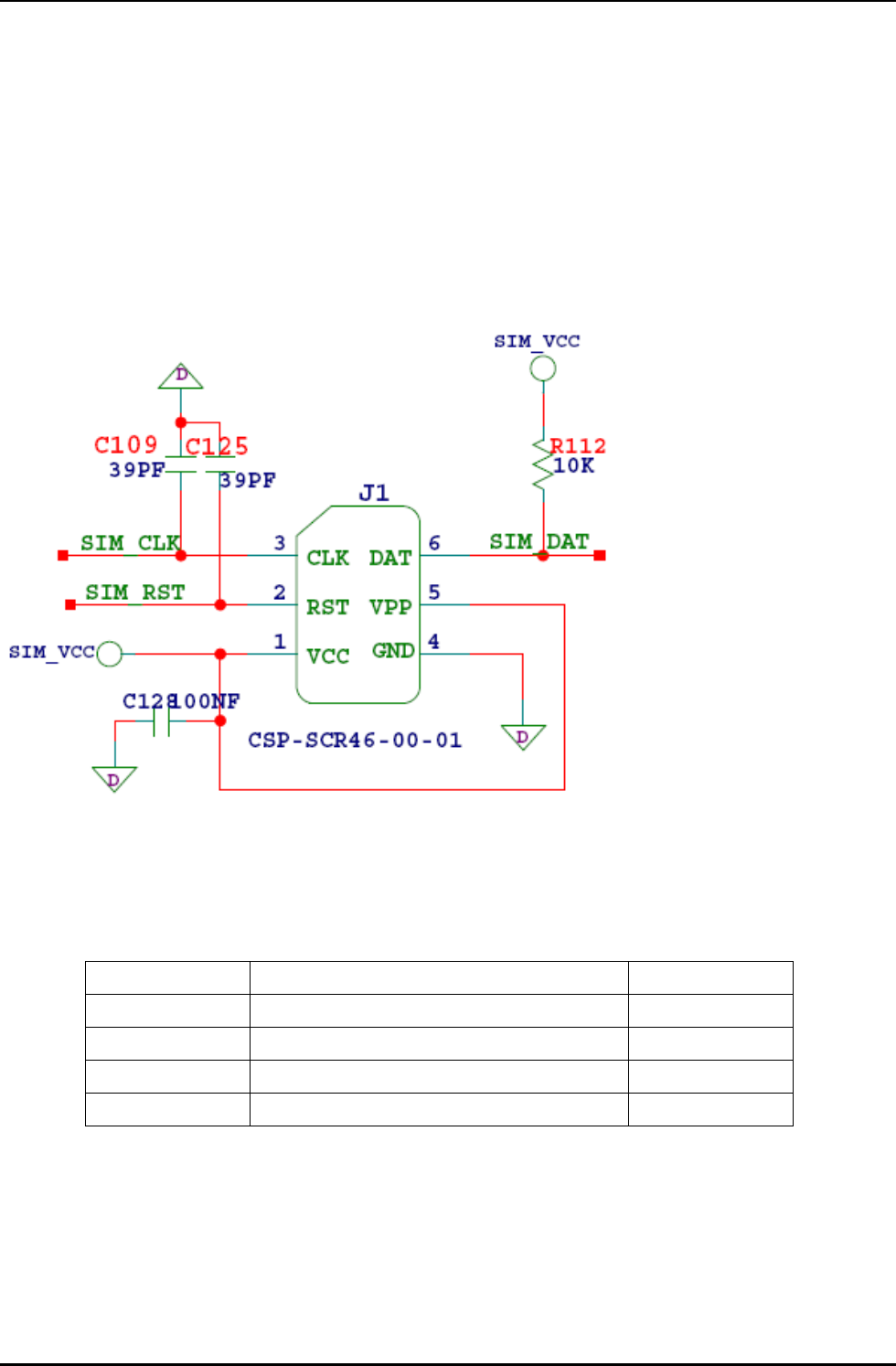
3.5.4 SIM Interface (pins 16, 17,18 &19)
The 80350 module’s built-in baseband processor has SIM card interface support compatible with ISO7816 IC
card standard. Each of the SIM card pins is connected to the corresponding pins of the baseband processor;
please refer to pin assignment defined in a preceding section. The following figure shows a reference
connection scheme of the SIM card slot, where C109,C125 and R112 are reserved, and are only used when
tuning to reduce EMI The user is free to disregard these optional components.
The SIM card interface supports 3V and 1.8V SIM cards.
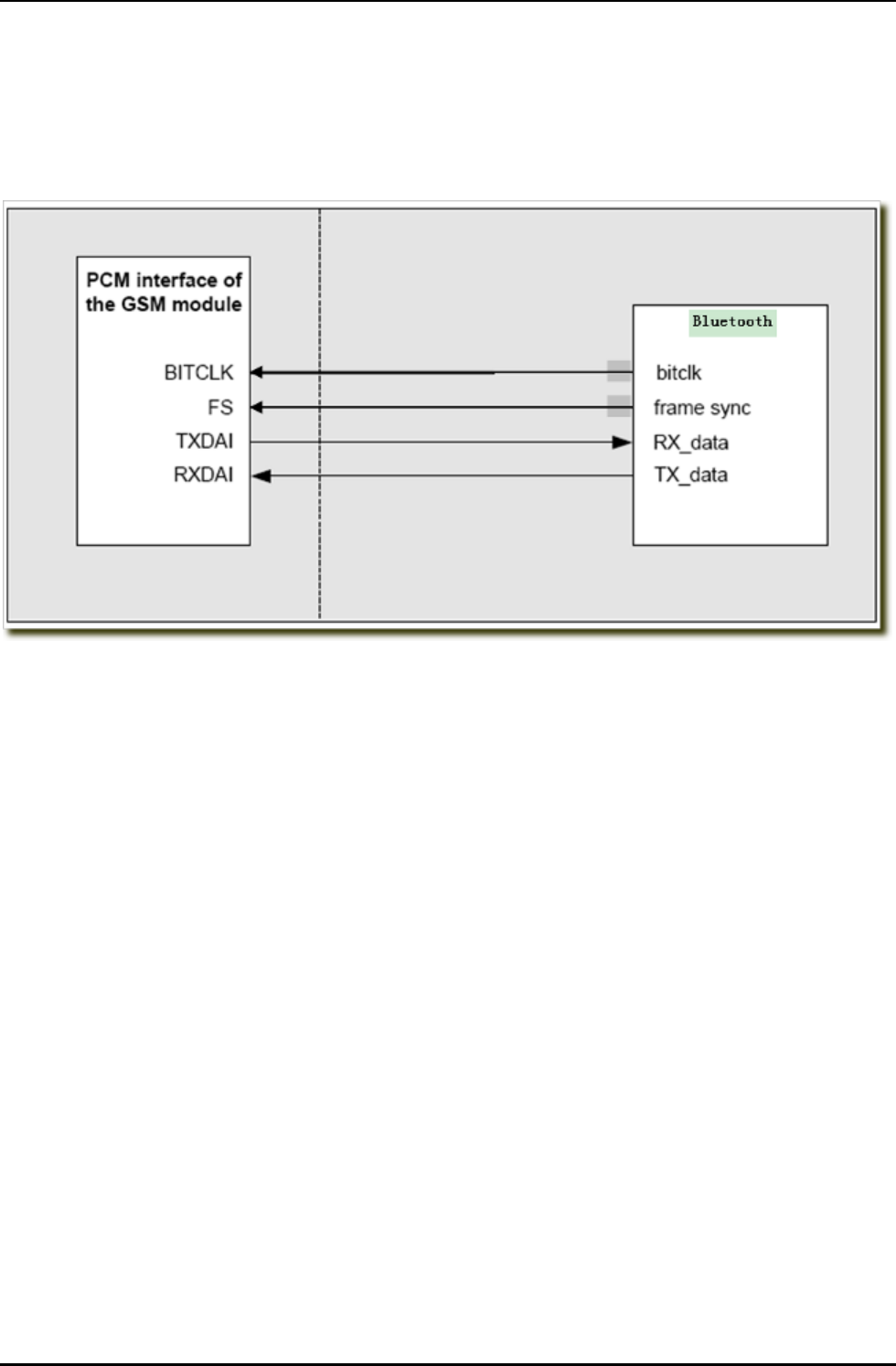
3.5.5 PCM Interface (pins 23, 24, 25 & 26)
The PCM can be used to connect the 80350 module with audio devices capable of PCM (Pulse Code
Modulation).
Interface Name Function Input/Output
PCM_TXD TXDAI Output
PCM_RXD RXDAI Input
PCM_SYNC Frame SYNC Output
PCM_CLK Bit Clock Output
80350 Module Integration Guide
11/10/2008 Confidential Page 30 of 53
For the PCM signal pins, please pay attention to the direction of I/O pinout. The 80350 module’s PCM codec
does not generate any clock signals, but only receive external PCM clock signal; hence, the module can act as
a slave PCM device, but not as a master device.
Next, more details on parameters and timing of PCM signal are presented. (Excerpts taken from the datasheet
of the PCM codec IC)
80350 Module Integration Guide
11/10/2008 Confidential Page 31 of 53
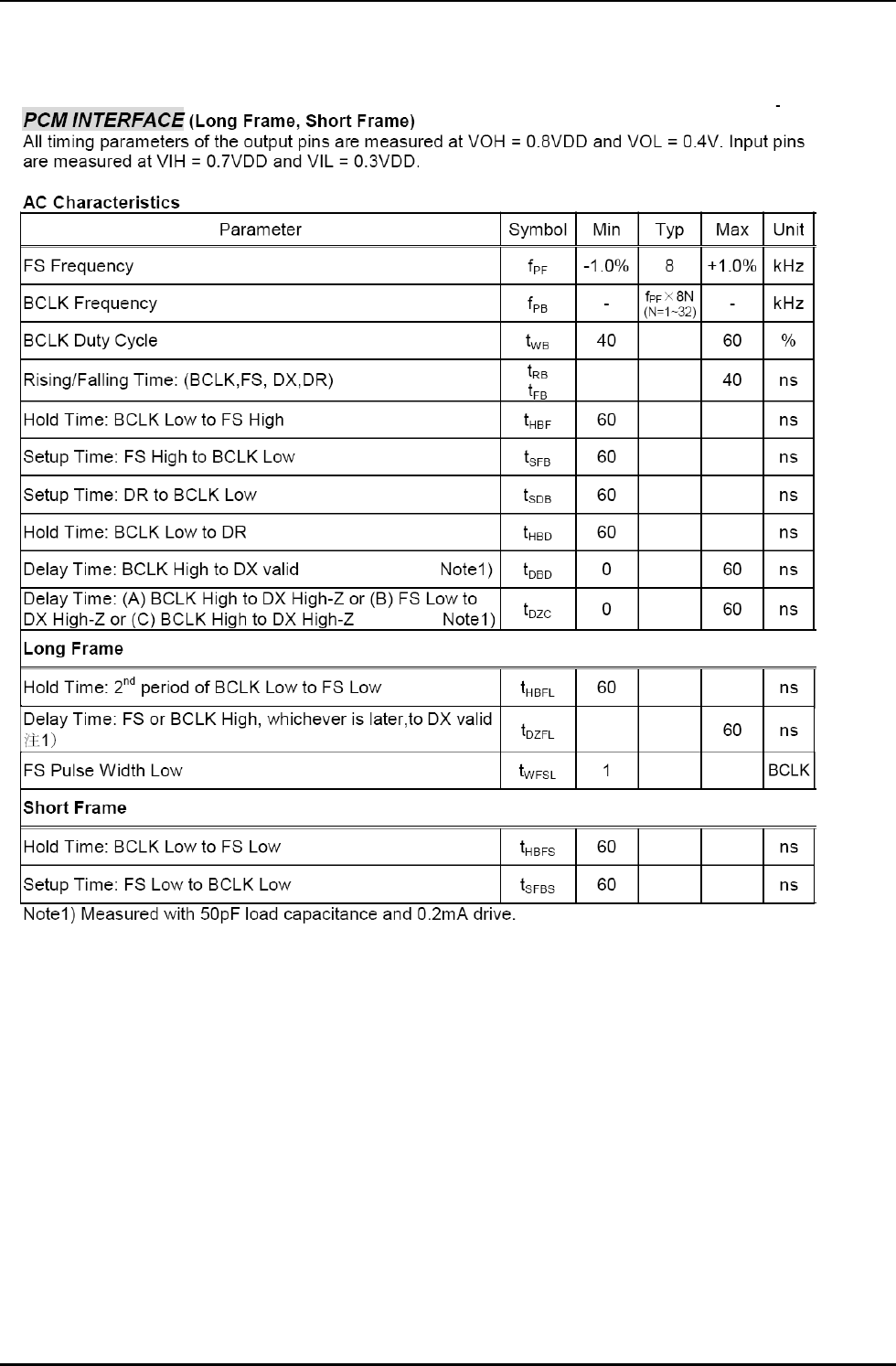
PCM interface timing and parameters
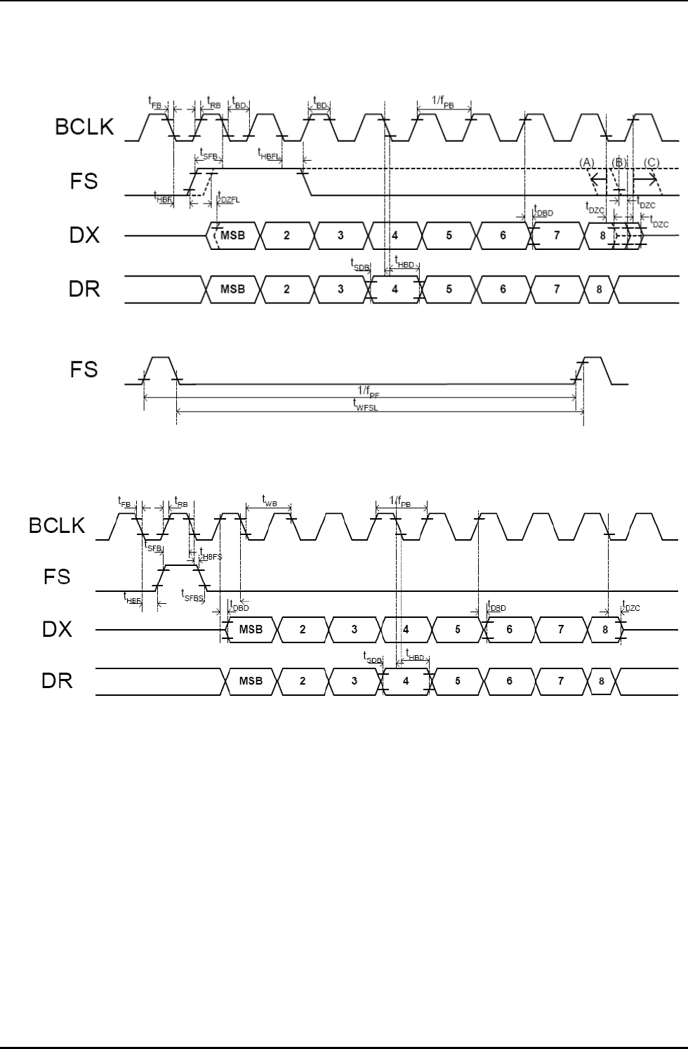
80350 Module Integration Guide
11/10/2008 Confidential Page 32 of 53
Figure 1: Long Frame timing
Figure 2: Short Frame timing
80350 Module Integration Guide
11/10/2008 Confidential Page 33 of 53
80350 Module Integration Guide
11/10/2008 Confidential Page 34 of 53
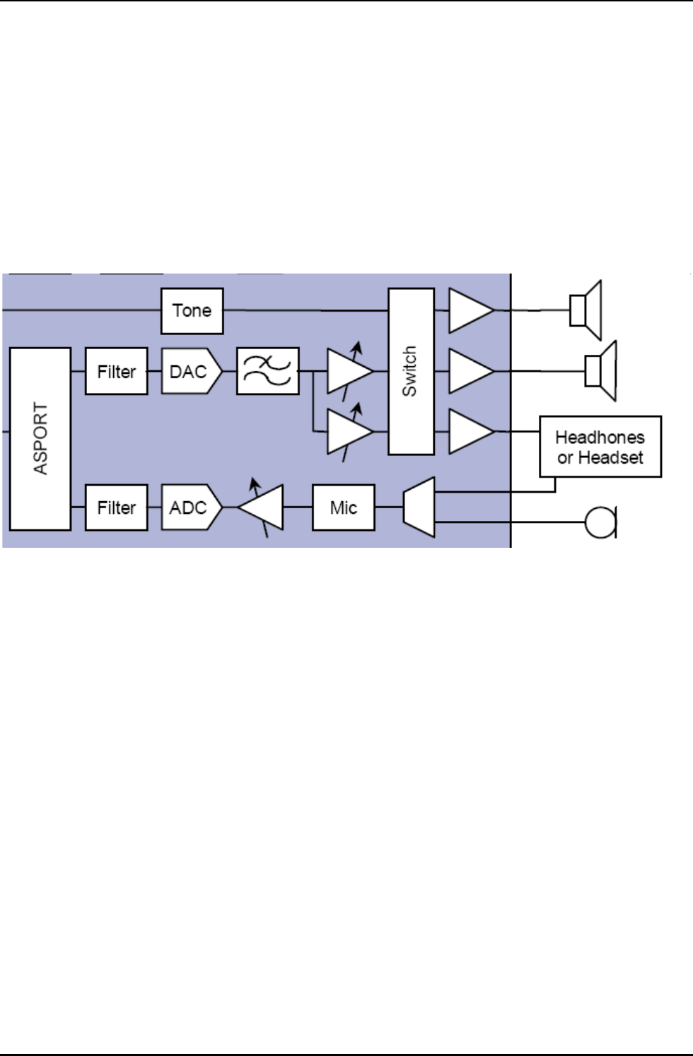
3.5.6 Auxiliary Audio Interface
The 80350 module allows four analog audio channels with physical interfaces on the board-to-board connector;
these channels are programmable by software:
• Two Auxiliary audio input interfaces, both with balanced or single-ended inputs.
• Two Auxiliary audio output interfaces, both with balanced or single-ended outputs.
This means that you can connect up to four different audio devices, although only one interface can be operated
at any given time. Using software command you can easily switch back and forth among the channels.
3.5.6.1 Auxiliary Audio output interface (Pins 62, 63, 64 & 65)
The analog output interface has two channels switchable by software. Specially,
A. SPKP/SPKN(pin62,63) Normal Differential Audio Output Specifications
80350 Module Integration Guide
11/10/2008 Confidential Page 35 of 53
B. RECP/RECN(Pin64,65), Normal Differential Audio Output Specifications
Note: For guidelines on the layout of Audio Output circuitry. please refer to Section 1.5.2.2.

80350 Module Integration Guide
11/10/2008 Confidential Page 36 of 53
3.5.6.2 Auxiliary Audio input interface (Pins 58, 59, 60 & 61)
There are two reserved channels for analog audio input:
Specification Typ. Units
Full-scale Input Voltage 2.0 Vpp
Input Resistance 10 Kohm
Comments:
A. For voice call, MIC1P/MIC1N interface is recommended as Audio Input.
B. On the 80350 module, only Audio Input interface is reserved. Except for the utility for microphone bias
voltage, the 80350 board possesses no specific microphone support circuitry; therefore, such needs to be taken
into account in the host board design.
C. For microphone circuitry layout, please refer to Section 1.5.2.2.
3.5.7 Serial Interface UART0
The module offers an 8-wire unbalanced, asynchronous modem interface ASC0.
The module is designed for use as a DCE. Based on the conventions for DTE-DCE connections it
communicates with the customer application (DTE) using the following signals:
• Port TXD @ application sends data to the module’s TXD0 signal line
• Port RXD @ application receives data from the module’s RXD0 signal line
Pin Name Pin Number Signal Direction Description
RXD0 30 I Serial data input (DTE <-- DCE)
TXD0 32 O Serial data output (DTE Æ DCE)
RTS0 49 O Request to send (DTE Æ DCE)
CTS0 52 I Clear to Send (DTE <-- DCE)
DCD0 54 I Data carrier detect (DTE <-- DCE)
DTR0 50 O Data terminal ready (DTE Æ DCE)
DSR0 48 I Data set ready (DTE <-- DCE)
RING0 47 I Ring detect output (DTE <-- DCE)
Note:
Pin Name and Signal Direction from HOST(DTE) Confirm, not the module.

80350 Module Integration Guide
11/10/2008 Confidential Page 37 of 53
3.5.8 Debug communication(Pins 10, 31)
The module can be calibrated by software through there two pins.
PINS Assignment Description Input/Output
10 DBGTX Debug transmitter Output
31 DBGRX Debug receiver Input

80350 Module Integration Guide
11/10/2008 Confidential Page 38 of 53
4. GSM/GPRS Services
The 8035 module supports the following GSM/GPRS services:
z Short Message Services (SMS)
z Class B GPRS Functionality
z Voice communication
z Circuit-switched data
4.1 Transmission Modes for the GSM/GPRS Services
Each of the GSM/GPRS services has two modes that can be enabled separately:
z Mobile-originated (MO): allows the making of a service request (such as making a telephone call or
sending an SMS)
z Mobile-terminated (MT): allows receiving a service request (such as receiving a telephone call or an SMS)
Note: Contact your local GSM operator to ensure that the services and modes have been provisioned for
the SIM card.
4.2 Voice Communication
The 80350 module supports voice functions. On the 80-pin board-to-board connector, there are reserved pins
for microphone and earphone hardware interfaces. When these are connected with microphone and earphone
hardware, the desired voice functions can be executed by invoking relevant commands in the AT Command set
(please refer to 80350 GSM/GPRS Modem Module AT Command Specification).
The 80350 module supports the following four audio coding formats:
1. Full-Rate (FR)
2. Enhanced Full-Rate (EFR)
3. Half-rate (HR)
4. Adaptive Multi-rate (AMR)
4.3 Circuit-Switched Data
In this mode, the 80350 module supports both of the connection modes of transmission that are provided by
GSM:
z Non-Transparent mode delivers a constantly low error rate but with a non-guaranteed throughput or
delay. The Non-Transparent service provides a performance that is closest to using a modem over a
fixed Public Switched Telephone Network (PSTN) line.
Note: All GSM service providers may not support transparent mode. In those cases, the 80350 module
can be configured to switch automatically to Non-Transparent mode. This capability depends on the
settings in the AT+CBST command.

80350 Module Integration Guide
11/10/2008 Confidential Page 39 of 53
4.4 Short Message Services(SMS)
The 80350 module can perform the following tasks for the GSM Short Message Services:
z Sending and receiving binary messages of up to 160 characters (7-bit characters)
z Sending and receiving text messages of up to 140 bytes (8-bit data)
z Submitting a SMS Protocol Data Unit (PDU) to a SMSC (Short Message Service Center) and storing a
copy of the PDU until either a report arrives from the network or a timer expires
z Receiving a SMS PDU from a SMSC
z Returning a delivery report to the network for a previously received message
z Receiving a report from the network
z Notifying the network when the module has sufficient memory capacity available to receive one or more
SMS messages (after the module had previously rejected a message because its memory capacity was
exceeded)
5. SIM Operation
5.1 Provisioning the SIM
The SIM card is configurable. To most users, the basic requirement on the SIM card is the ability to configure
and use voice call and SMS Receive services, while some users may further need SMS Send and GPRS data
services. The 80350 module can meet the MO (Mobile-Originated) and MT (Mobile-Terminated) usage
requirements, and can configure the relevant services of the SIM card through AT commands (this will need
support from the application layer software).
5.2 GSM Supported Services
The 80350 module supports the following services:
z Voice calls (MO and MT): requires a telephone number
z SMS (MO and MT): requires a telephone number
z Circuit-switched data calls (MO and MT): requires a telephone number
z The GSM SIM can have multiple telephone numbers.
Note: The services depend on the actual network; please contact the network operator in order make sure that
the services are enabled.

80350 Module Integration Guide
11/10/2008 Confidential Page 40 of 53
5.3 GPRS Supported Services
The 80350 module supports the following GPRS (modes of operation) that must be enabled by the operator:
z GPRS Packet Connectivity (MO and MT) with Both Dynamic and Static IP option
z GPRS SMS (MO and MT): uses the IP (Dynamic or Static) set by the operator
z Multiple APN Setting
z Quality of Service Options
z Multi-slot 10 Class of Service
5.4 GSM Modes of Operation
When provisioning the SIM for the 80350 module, enable the following modes of operation:
z Voice calls: configure the SIM for both MO and MT service (to send and receive)
z SMS: configure the SIM either for MT alone (to receive) or for both MO and MT (to send and receive)
z Circuit Switched Data: configure the SIM either for MO alone (to send) or for both MO and MT (to send
and receive)
Voice SMS CS
Data GPRS Function
MO/MT MT MO Voice calls, receive SMS, make data calls
MO/MT MO/MT MO Voice calls, receive / send SMS, make data calls
MO/MT MO/MT MO/MT Voice calls, receive / send SMS, make / receive data calls
(requires an additional data telephone number)

80350 Module Integration Guide
11/10/2008 Confidential Page 41 of 53
6. Software Interface
6.1 API Interface
The 80350 module’s default startup mode is the AT command mode. In this mode, PC Super Terminal or other
serial port communication tools may be used to issue AT commands to the module.
The 80350 module’s default serial communication is set at 115200 baud, no parity, 8 data bits, 1 stop bit, and no
flow control. A user can send/receive AT commands, data, or response to/from the module via one of the two
methods:
z Straight serial communication via HyperTerminal or similar application
Straight serial communication provides the user with the following capabilities:
z Send AT commands and receive response
z Receive SMS notification
z Make a voice, data or fax call
z Receive any unsolicited message
6.2 AT Command Set
This is addressed separately in the document “80350 GSM/GPRS Modem Module AT Command
Specification”.
80350 Module Integration Guide
11/10/2008 Confidential Page 42 of 53
7. Setup and Initialization
The 80350 module can be controlled by AT command through the COM Port A on the 80350 motherboard.
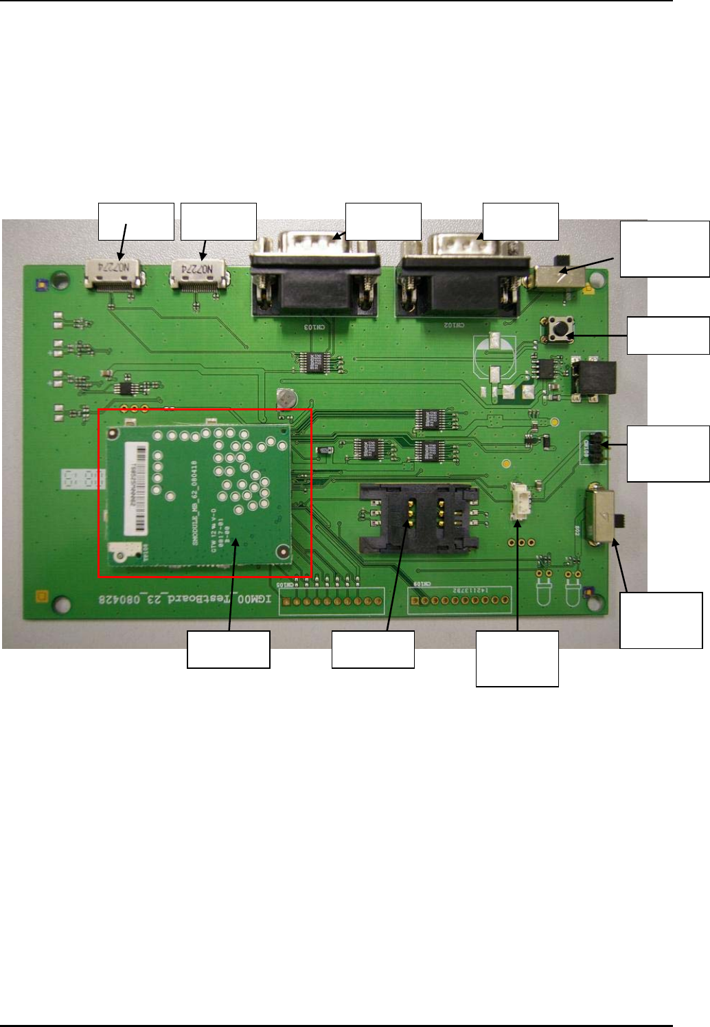
80350 Motherboard Outline:
80350 Motherboard
I/O Port B I/O Port A COM Port B COM Port A
Module On
Trigger
Reset Key
Power
Connector B
Power On/Off
Switch
Power
Connector A
SIM Holder 80350 Module
+
-
+
-
On
Off
On
80350 Module
80350 Module Integration Guide
11/10/2008 Confidential Page 43 of 53
Parts: Item Function Comments
I/O Port A Reserved
I/O Port B Reserved
COM Port A COM port to communicate with PC DB9 Connector
COM Port B Reserved
Power Connector A Connect with power supply DC 3.55 to 4.2 V
Power Connector B Connect with power supply DC 3.55 to 4.2 V
Power On/Off Switch On/Off the power
Module On Trigger Power On the module
Reset Key Reset the module
80350 Module The 80350 Module
SIM Holder Using for SIM card
Steps for setting up the testing hardware environment:
1. Install the 80350 module to the 80350 motherboard
2. Put the SIM card into the SIM Holder
3. Plug the power supply to any one of the Power Connector.
4. Power on the 80350 module by switch the GSM On Trigger to “On”.
7.1 Initialization
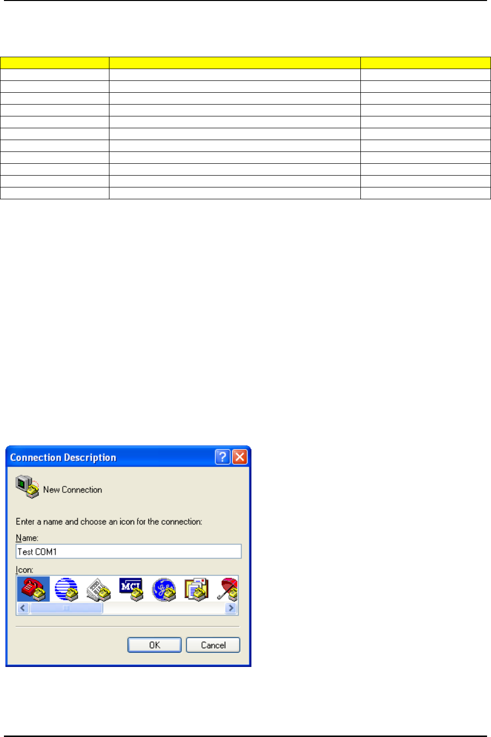
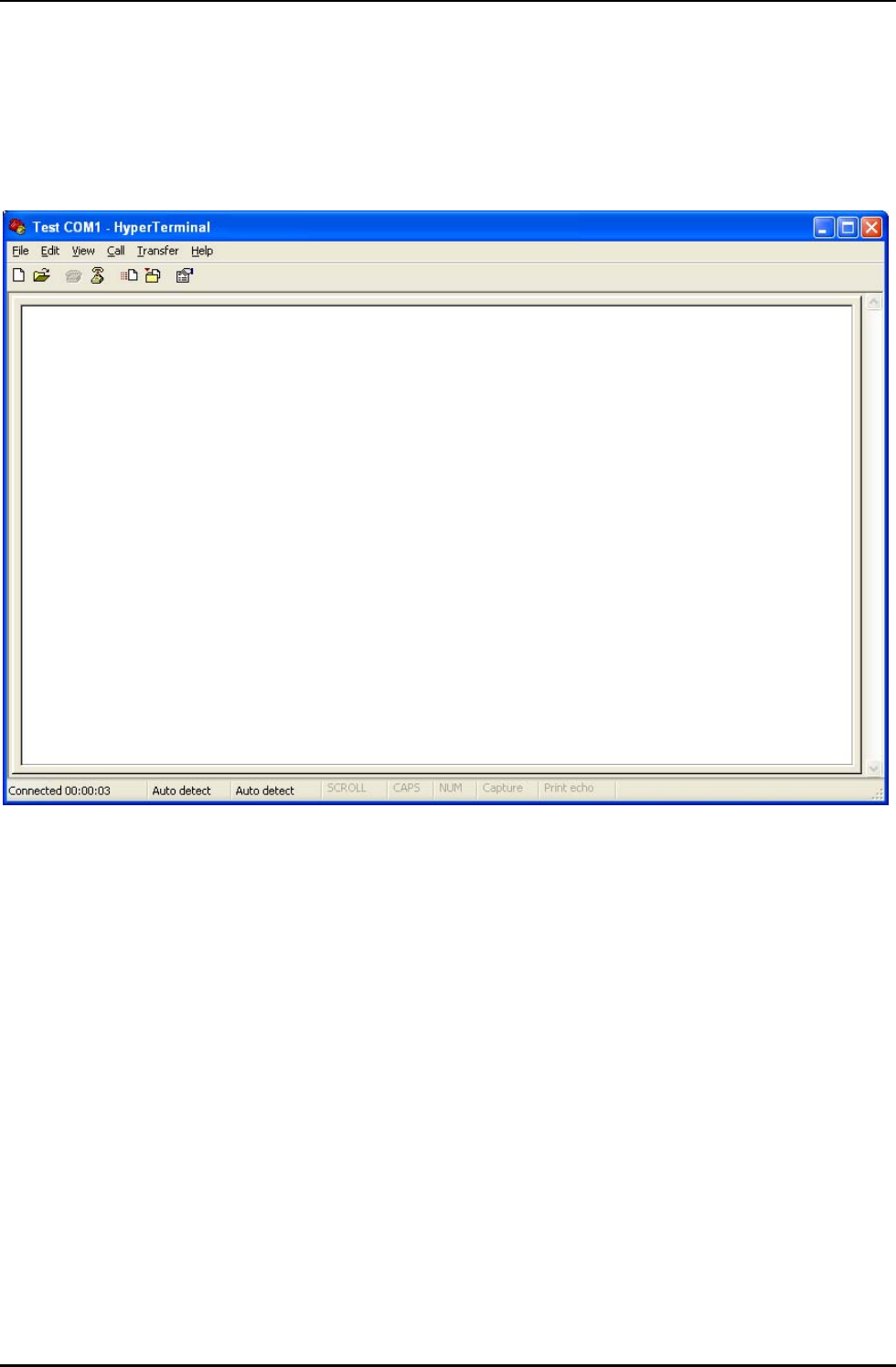
7.1.1 Start HyperTerminal
On Windows XP, click on:
Start>Programs>Accessories>Communications>HyperTerminal
1. You should see the following screen.
2. Enter a name for the Connection. In this example, the Name is Test COM1.
3. Click OK.
80350 Module Integration Guide
11/10/2008 Confidential Page 44 of 53
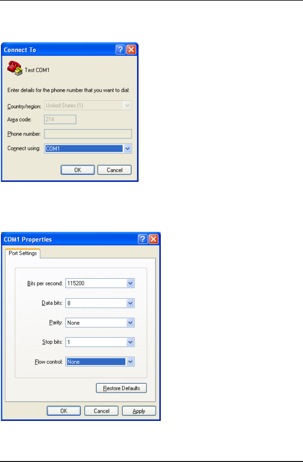
4. The next window that will appear is the Connect To window.
5. Change the Connect Using setting to the Com port that was determined in Step 2.
6. Click OK.
7. The next window is the Port Settings window.
80350 Module Integration Guide
11/10/2008 Confidential Page 45 of 53
8. Make sure the settings match the example.
9. Click OK.
10. Now the Main Program Window should appear.
11. Terminal Setup Testing.
a. Make sure the cursor is in the main window.
b. Type “AT” and press “Enter”
c. You should see the module responds back with “OK” in the Main Window
d. If this happens, the COM port is configured correctly.
e. At this point you are ready to configure and test the 80350 with AT commands.

80350 Module Integration Guide
11/10/2008 Confidential Page 46 of 53
7.1.2 Initialization Command
After the module power on, user can initialize the module by following AT commands
Unsolicite
d *TSYSSTART System start
Unsolicite
d +CFUN: 1 Full functionality (Default)
Entry ATE1 Echo mode on
Response OK Command is valid
Entry AT&D1 ON->OFF on DTR: Change to command mode with call
remaining connected
Response OK Command is valid
Entry ATS0=0 automatic answering is disabled
Response OK Command is valid
Entry AT+CMEE=1 enable result code and use numeric values
Response OK Command is valid
Entry AT+CRC=1 the extended format of incoming call
indication is used
Response OK Command is valid
Entry AT+CREG=1 enable network registration unsolicited result code +CREG: <stat>
Response OK Command is valid
Entry AT+COPS=3,2 set only <format> (for read command +COPS?) – not shown in Read
command response and short format alphanumeric <oper>
Response OK Command is valid
Entry AT+VTD=3 duration of the tone in 1/10 seconds
Response OK Command is valid
Entry AT+CCWA=1 enable presentation of an unsolicited result code
Response OK Command is valid
Entry AT+CLIP=1 display unsolicited result codes
Response OK Command is valid
Entry AT+CMUT=0 mute off
Response OK Command is valid

80350 Module Integration Guide
11/10/2008 Confidential Page 47 of 53
7.2 Send SMS Example
Entry AT+CMGF=1 Select SMS format is text
Respons
e OK Command is valid
Entry AT+CNMI=2,2,2,0,0 New SMS unsolicited result code: +CMT:
Respons
e OK Command is valid
Entry AT+CSCS="IRA" Select international reference alphabet
Respons
e OK Command is valid
Entry AT+CSCA="987654321" Select SMS Service Centre Address
Respons
e OK Command is valid
Entry AT+CMGS="123456789" Send a message to 123456789
Respons
e > Ready to enter a message.
Entry This is a test message^Z Enter the text message “This is a test
message”. End the message with Control
Z.
Respons
e +CMGS: 1
OK Successful transmission. The number
will increment with each SMS sent.
Entry AT+CMGL= "ALL" List All messages from preferred store
Respons
e +CMGL:1,"REC
READ","+123456789",,"08/08/08,18:02:15+32"
M
OK
List all message
Entry AT+CMGR=1 Read SMS message in preferred store 1
Respons
e +CMGR: "REC
READ","+987654321",,"08/08/08,18:02:15+32"
M
OK
Read 1 message
Entry AT+CMGD= 1 Delete SMS message in preferred store
1.
Respons
e OK Successful delete

80350 Module Integration Guide
11/10/2008 Confidential Page 48 of 53
7.3 Voice Call Example
7.3.1 MO
The call is OK:
Entry ATD10086; Make a call
Unsolicite
d +WIND: 5,1 The call (id =1) has been established
Response OK Command is valid
Unsolicite
d +WIND: 2 The MT is ringing
Unsolicite
d +WIND: 9,1 The call is connected
Entry ATH End the call
Unsolicite
d +WIND: 6,1 The call is disconnected
Response OK Command is valid
MT is busy:
Entry ATD10086; Make a call
Unsolicite
d +WIND: 5,1 The call (id =1) has been established
Response OK Command is valid
Unsolicite
d +WIND: 6,1 The call is disconnected
Unsolicite
d BUSY MT is busy
MT can’t be connected:
Entry ATD10086; Make a call
Unsolicite
d +WIND: 5,1 The call (id =1) has been established
Response OK Command is valid
Unsolicite
d +WIND: 6,1 The call is disconnected
Unsolicite
d NO CARRIER MT cannot be connected
7.3.2 MT
Unsolicite
d +WIND: 5,1 The call (id =1) has been established
Unsolicite
d RING The MT is ringing
Entry ATA Accept the call
Response OK Command is valid
Unsolicite
d +WIND: 9,1 The call is connected

80350 Module Integration Guide
11/10/2008 Confidential Page 49 of 53
7.4 GPRS Packet Examples
After the module register on a GSM network:
Entry AT+CGATT=1 AT command to start the ATTACH sequence
Response OK Successfully Attached
If the network is a transparent network, then you can activate using HyperTerminal. If it is non
transparent, you have to use a PPP link to activate:
Entry AT+CGDCONT=1,”IP”,”CMWAP”,””,0,
0 CMWAP value will be provided by carrier
Response OK Command is valid
Entry AT+CGACT=1,1 Request context activation.
Response OK Successful context activation.
GPRS detach and deactivate:
Entry AT+CGACT=0,1 AT command to deactivate.
Response OK Successful deactivation.
Entry AT+CGATT=0 AT command to detach.
Response OK Successful detach.

80350 Module Integration Guide
11/10/2008 Confidential Page 50 of 53
References
1. AT Command Set Reference [80350 GSM/GPRS Modem Module AT Command Specification]
2. GSM 07.05: “Digital cellular telecommunications systems (Phase 2+); Use of Data Terminal Equipment –
Data Circuit terminating Equipment (DTE – DCE) interface for Short Message Service (SMS) and Cell
Broadcast Service (CBS)”.
3. GSM 07.07: “Digital cellular telecommunications systems (Phase 2+); AT command set for GSM Mobile
Equipment (ME)”.
4. ITU-T Draft new Recommendation V.25ter: “Serial asynchronous automatic dialing and control”.
5. AD6720 Technical Data (REV. OCTOBER 18,2005)
6. NARROW-PITCH CONNECTORS Specifications (Jul.13, 2006)
7. U.FL-R-SMT (10) Specifications (Apr.17, 1997)
8. AK2301-MS0416-1-00 Specifications (Aug 31, 2005)

80350 Module Integration Guide
11/10/2008 Confidential Page 51 of 53
Abbreviation
Abbreviation Description
ADC Analog-to-Digital Converter
AFC Automatic Frequency Control
AGC Automatic Gain Control
ANSI American National Standards Institute
ARFCN Absolute Radio Frequency Channel Number
ARP Antenna Reference Point
ASC0 / ASC1 Asynchronous Serial Controller. Abbreviations used for first and second serial inter-
face of MC55i
ASIC Application Specific Integrated Circuit
B Thermistor Constant
B2B Board-to-board connector
BER Bit Error Rate
BTS Base Transceiver Station
CB or CBM Cell Broadcast Message
CE Conformité Européene (European Conformity)
CHAP Challenge Handshake Authentication Protocol
CPU Central Processing Unit
CS Coding Scheme
CSD Circuit Switched Data
CTS Clear to Send
DAC Digital-to-Analog Converter
DAI Digital Audio Interface
dBm0 Digital level, 3.14dBm0 corresponds to full scale, see ITU G.711, A-law
DCE Data Communication Equipment (typically modems, e.g. Siemens GSM engine)
DCS 1800 Digital Cellular System, also referred to as PCN
DRX Discontinuous Reception
DSB Development Support Box
DSP Digital Signal Processor
DSR Data Set Ready
DTE Data Terminal Equipment (typically computer, terminal, printer or, for example, GSM
application)
DTR Data Terminal Ready
DTX Discontinuous Transmission
DUN Dial-Up Networking

80350 Module Integration Guide
11/10/2008 Confidential Page 52 of 53
EFR Enhanced Full Rate
EGSM Enhanced GSM
Abbreviation Description
EMC Electromagnetic Compatibility
ESD Electrostatic Discharge
ETS European Telecommunication Standard
FCC Federal Communications Commission (U.S.)
FDMA Frequency Division Multiple Access
FR Full Rate
GMSK Gaussian Minimum Shift Keying
GPRS General Packet Radio Service
GSM Global Standard for Mobile Communications
HiZ High Impedance
HR Half Rate
I/O Input/Output
IC Integrated Circuit
IMEI International Mobile Equipment Identity
ISO International Standards Organization
ITU International Telecommunications Union
kbps kbits per second
LED Light Emitting Diode
Li-Ion Lithium-Ion
Mbps Mbits per second
MMI Man Machine Interface
MO Mobile Originated
MS Mobile Station (GSM engine), also referred to as TE
MSISDN Mobile Station International ISDN number
MT Mobile Terminated
NTC Negative Temperature Coefficient
OEM Original Equipment Manufacturer
PA Power Amplifier
PAP Password Authentication Protocol
PBCCH Packet Switched Broadcast Control Channel
PCB Printed Circuit Board
PCL Power Control Level
PCM Pulse Code Modulation

80350 Module Integration Guide
11/10/2008 Confidential Page 53 of 53
PCN Personal Communications Network, also referred to as DCS 1800
PCS Personal Communication System, also referred to as GSM 1900
PDU Protocol Data Unit
Abbreviation Description
PLL Phase Locked Loop
PPP Point-to-point protocol
PSU Power Supply Unit
R&TTE Radio and Telecommunication Terminal Equipment
RAM Random Access Memory
RF Radio Frequency
RMS Root Mean Square (value)
ROM Read-only Memory
RTC Real Time Clock
Rx Receive Direction
SAR Specific Absorption Rate
SELV Safety Extra Low Voltage
SIM Subscriber Identification Module
SMS Short Message Service
SRAM Static Random Access Memory
TA Terminal adapter (e.g. GSM engine)
TDMA Time Division Multiple Access
TE Terminal Equipment, also referred to as DTE
Tx Transmit Direction
UART Universal asynchronous receiver-transmitter
URC Unsolicited Result Code
USSD Unstructured Supplementary Service Data
VSWR Voltage Standing Wave Ratio