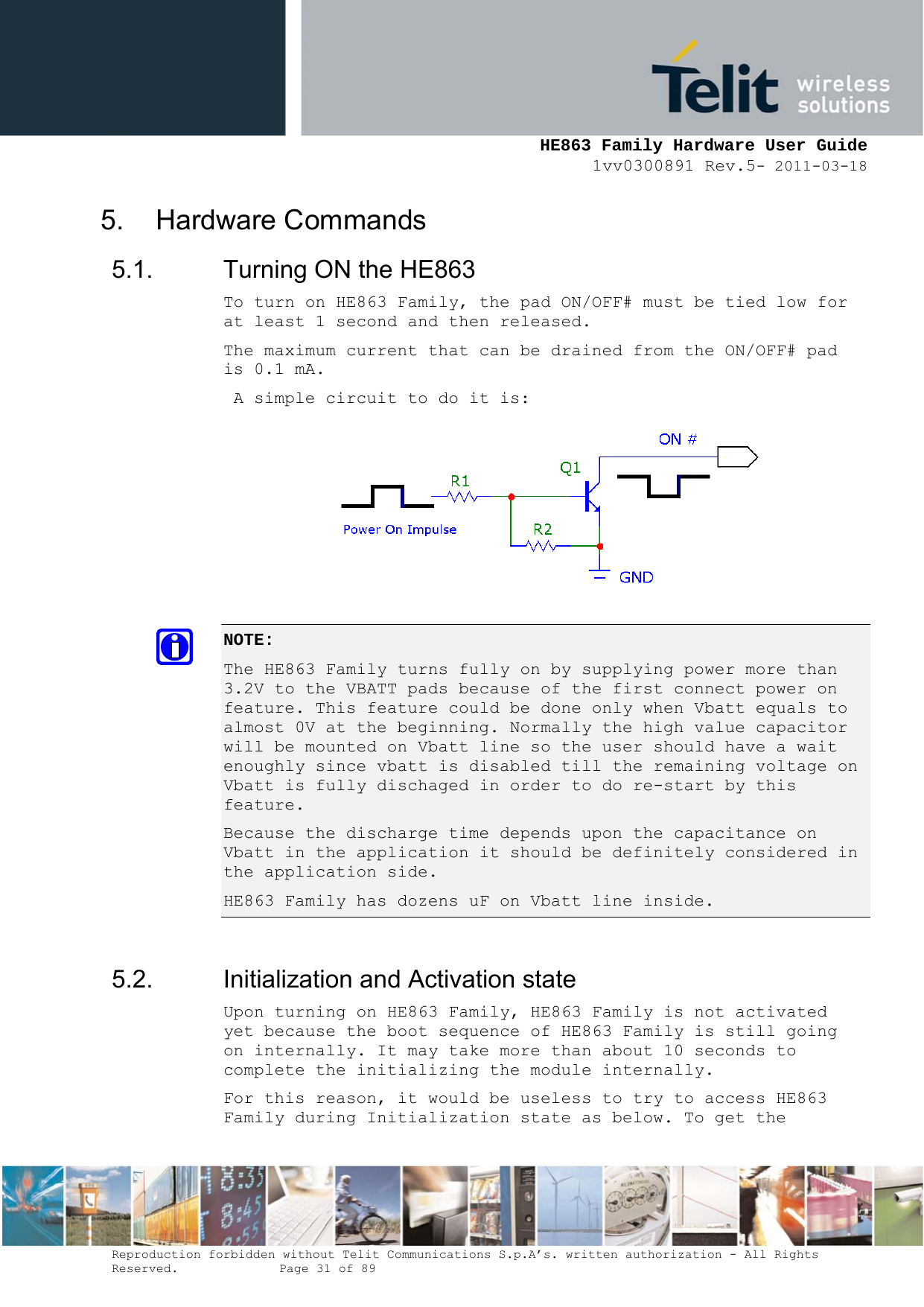
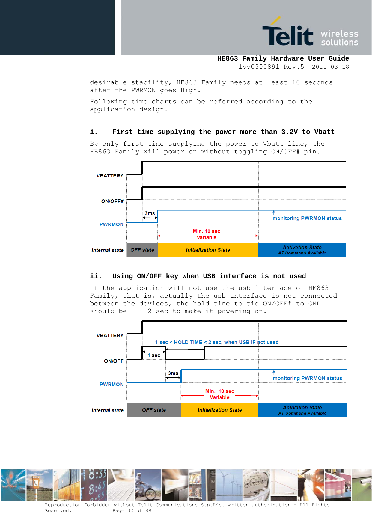
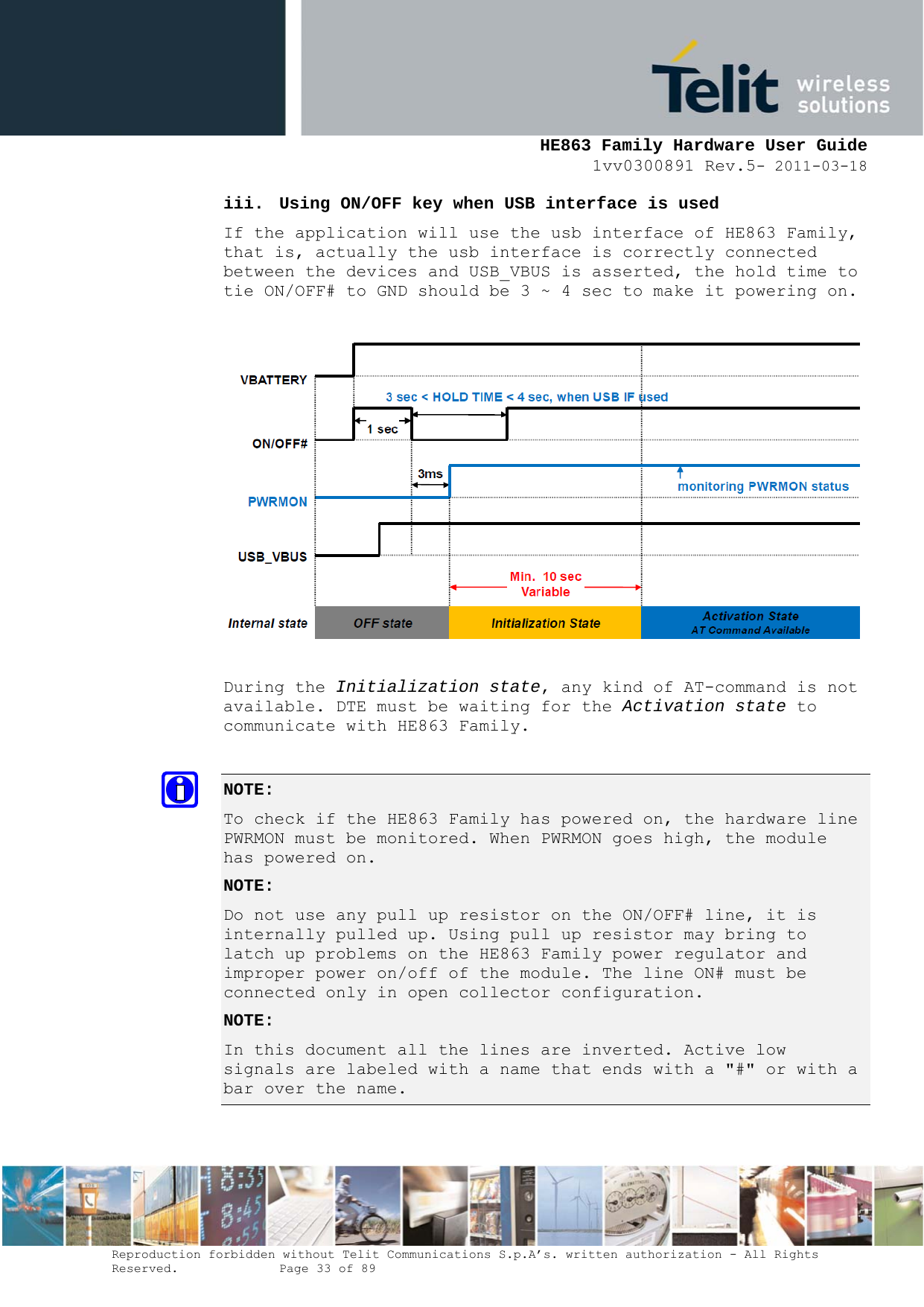
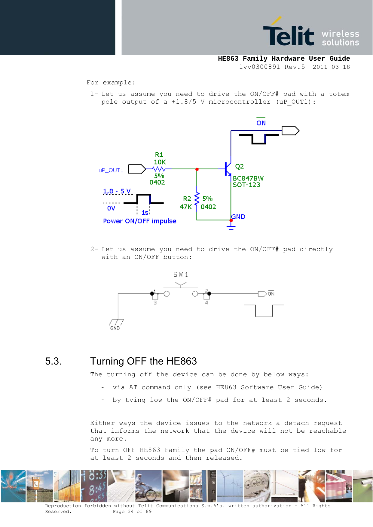
Tyco Safety Canada 123G260R DUAL ALARM COMMUNICATOR User Manual USERS GUIDE
Digital Security Controls Ltd. DUAL ALARM COMMUNICATOR USERS GUIDE
UserManual.wiki
>
Tyco Safety Canada
>
123G260R User Manual
>
USERS GUIDE
Contents
1.
USERS GUIDE
2.
USERS MANUAL
USERS GUIDE
Navigation menu
Upload a User Manual
Namespaces
Wiki Guide
HTML
PDF
Info
Views
User Manual
Discussion / Help
Navigation


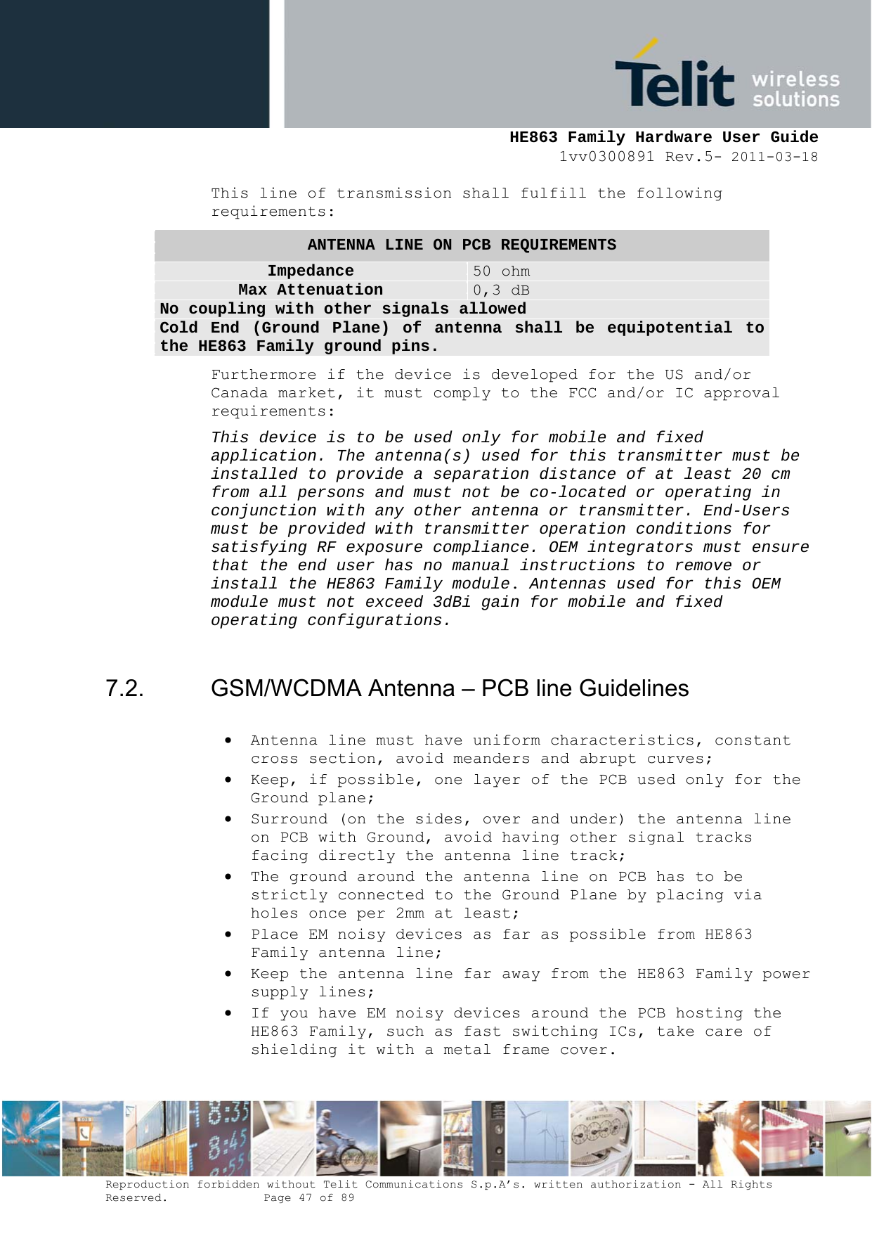

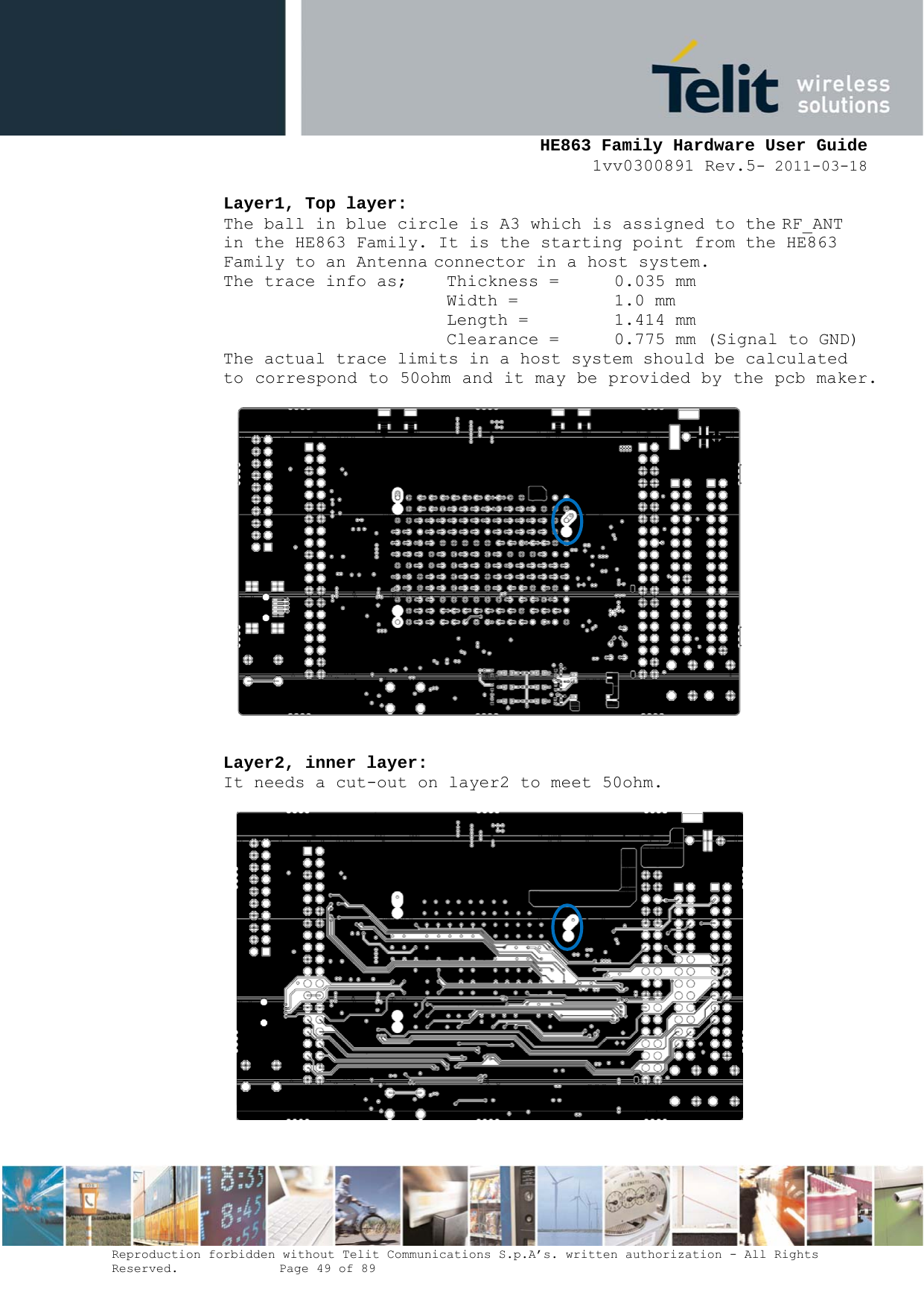


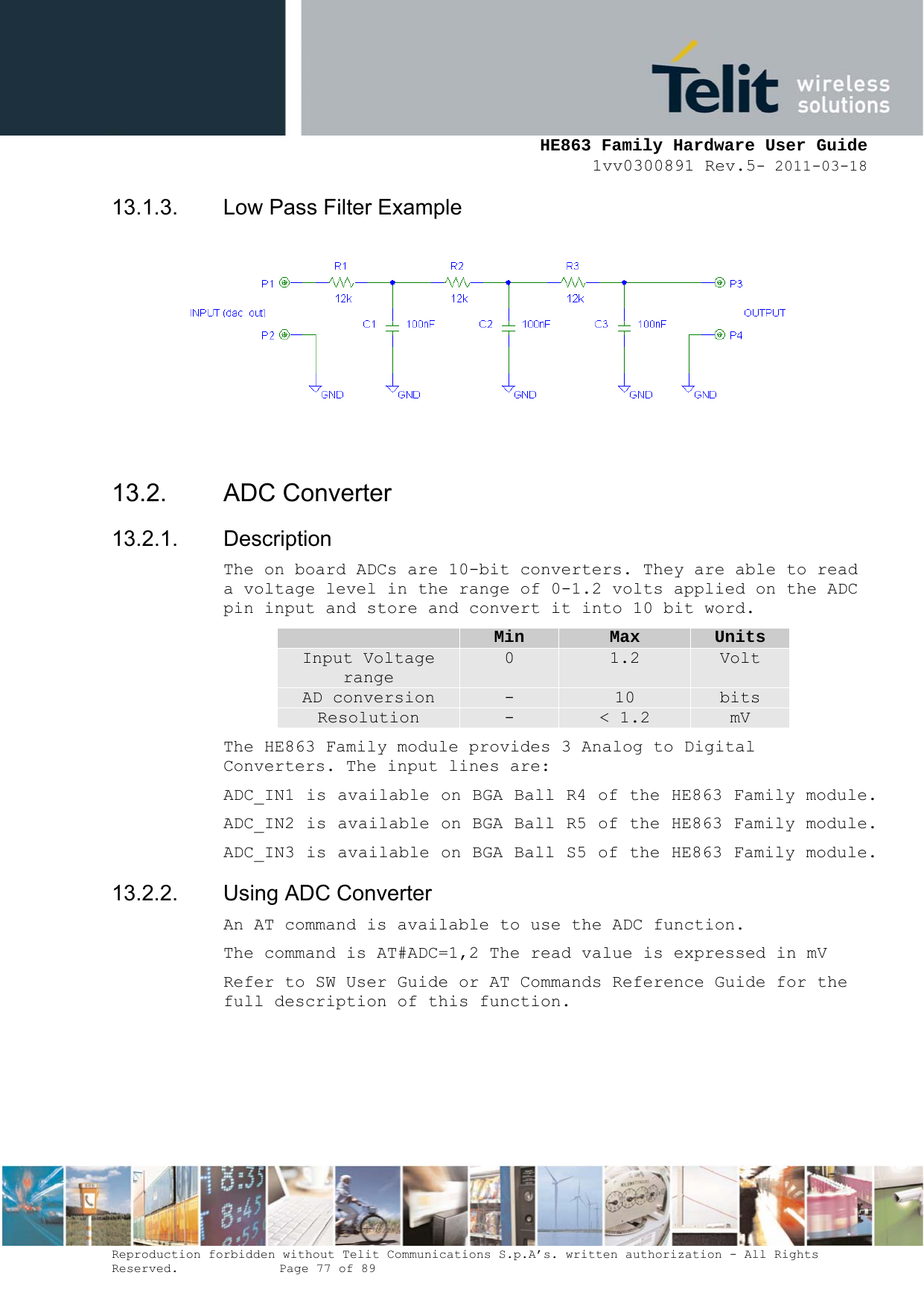
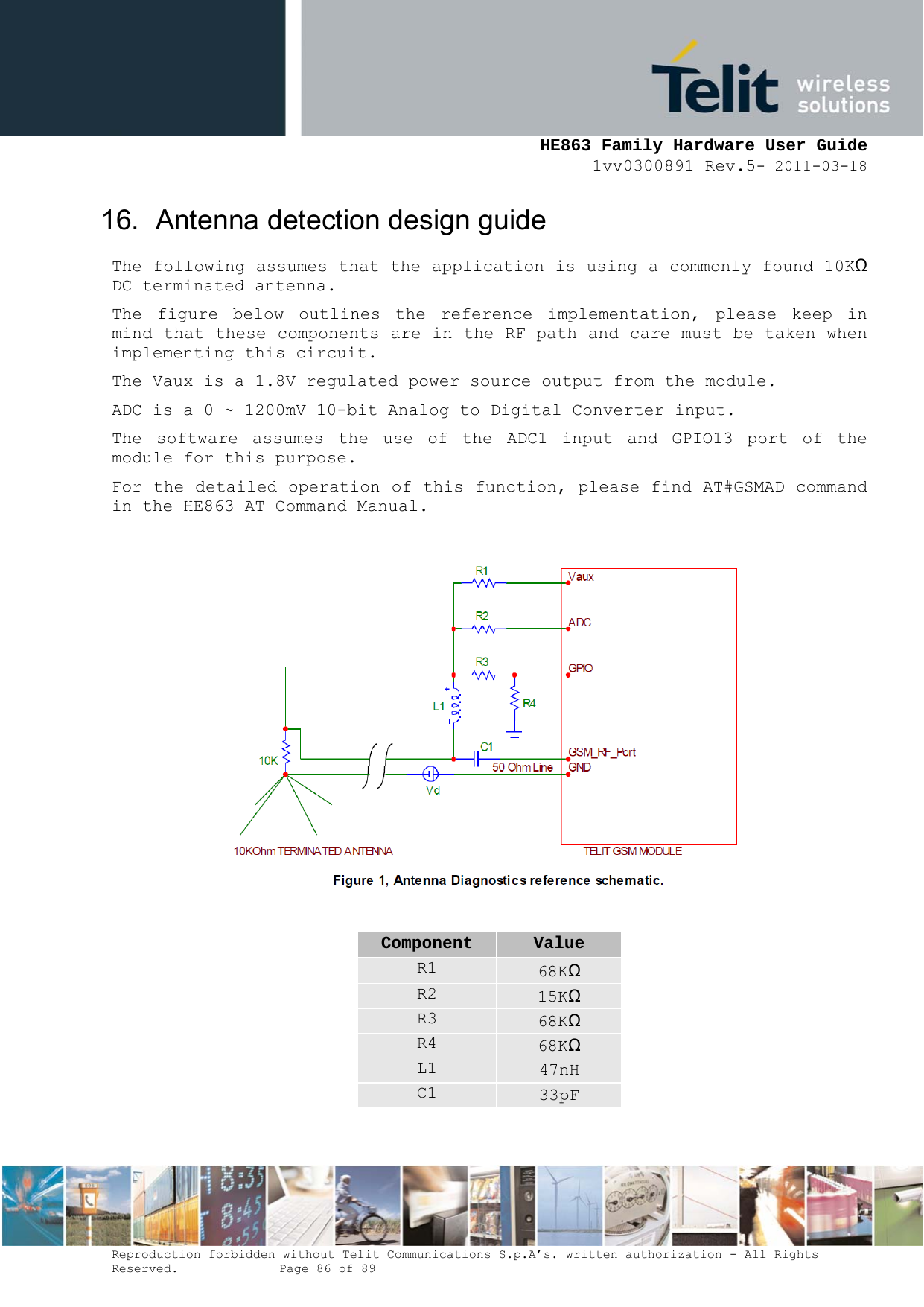
![HE863 Family Hardware User Guide 1vv0300891 Rev.5- 2011-03-18 Reproduction forbidden without Telit Communications S.p.A’s. written authorization - All Rights Reserved. Page 76 of 89 13. DAC and ADC section 13.1. DAC Converter 13.1.1. Description The HE863 Family module provides a Digital to Analog Converter. The signal (named DAC_OUT) is available on BGA Ball S4 of the HE863 Family module. The on board DAC is a 16-bit converter, able to generate an analogue value based on a specific input in the range from 0 up to 65535 but recalibrated in the range from 0 to 1023. However, an external low-pass filter is necessary. Min Max Units Voltage range (filtered) 0 1.8 Volt Range 0 1023 Steps The precision is 1023 steps, so if we consider that the maximum voltage is 1.8V, the integrated voltage could be calculated with the following formula: Integrated output voltage = 1.8 * value / 1023 DAC_OUT line must be integrated (for example with a low band pass filter) in order to obtain an analog voltage. 13.1.2. Enabling DAC An AT command is available to use the DAC function. The command is:AT#DAC[=<enable>[,<value>]] <value> - scale factor of the integrated output voltage (0..1023 - 10 bit precision) it must be present if <enable>=1 Refer to SW User Guide or AT Commands Reference Guide for the full description of this function. NOTE: The DAC frequency is selected internally. D/A converter must not be used during POWERSAVING.](https://usermanual.wiki/Tyco-Safety-Canada/123G260R.USERS-GUIDE/User-Guide-1690411-Page-76.png)