Tyco Safety Canada 123G260R DUAL ALARM COMMUNICATOR User Manual USERS GUIDE
Digital Security Controls Ltd. DUAL ALARM COMMUNICATOR USERS GUIDE
Contents
- 1. USERS GUIDE
- 2. USERS MANUAL
USERS GUIDE

HE863 Family
Hardware User Guide
1vv0300891 Rev.5 – 2011-03-18
HE863 Family Hardware User Guide
1vv0300891 Rev.5- 2011-03-18
Reproduction forbidden without Telit Communications S.p.A’s. written authorization - All Rights
Reserved. Page 2 of 89
APPLICABLE PRODUCT
P
RODUCT
H
E
863
-
E
UD
H
E
863
-
E
U
R
H
E
863
-
E
UG
H
E
863
-
NAD
H
E
863
-
N
A
R
H
E
863
-
NAG
H
E
863
-
AUD
H
E
863
-
AUG

HE863 Family Hardware User Guide
1vv0300891 Rev.5- 2011-03-18
Reproduction forbidden without Telit Communications S.p.A’s. written authorization - All Rights
Reserved. Page 3 of 89
Disclaimer
The information contained in this document is the proprietary
information of Telit Communications S.p.A. and its affiliates
(“TELIT”).
The contents are confidential and any disclosure to persons
other than the officers, employees, agents or subcontractors
of the owner or licensee of this document, without the prior
written consent of Telit, is strictly prohibited.
Telit makes every effort to ensure the quality of the
information it makes available. Notwithstanding the foregoing,
Telit does not make any warranty as to the information
contained herein, and does not accept any liability for any
injury, loss or damage of any kind incurred by use of or
reliance upon the information.
Telit disclaims any and all responsibility for the
application of the devices characterized in this document, and
notes that the application of the device must comply with the
SAFETY standards of the applicable country, and where
applicable, with the relevant wiring rules.
Telit reserves the right to make modifications, additions and
deletions to this document due to typographical errors,
inaccurate information, or improvements to programs and/or
equipment at any time and without notice.
Such changes will, nevertheless be incorporated into new
editions of this document.
Copyright: Transmittal, reproduction, dissemination and/or
editing of this document as well as utilization of its
contents and communication thereof to others without express
authorization are prohibited. Offenders will be held liable
for payment of damages. All rights are reserved.
Copyright © Telit Communications S.p.A. 2010.

HE863 Family Hardware User Guide
1vv0300891 Rev.5- 2011-03-18
Reproduction forbidden without Telit Communications S.p.A’s. written authorization - All Rights
Reserved. Page 4 of 89
Contents
1. INTRODUCTION.................................................................................................................................................6
1.1. SCOPE.................................................................................................................................................................6
1.2. AUDIENCE............................................................................................................................................................6
1.3. CONTACT INFORMATION, SUPPORT...................................................................................................................6
1.4. DOCUMENT ORGANIZATION................................................................................................................................7
1.5. TEXT CONVENTIONS...........................................................................................................................................8
1.6. RELATED DOCUMENTS.......................................................................................................................................8
1.7. DOCUMENT HISTORY..........................................................................................................................................9
2. OVERVIEW.......................................................................................................................................................11
2.1. HE863FAMILYPRODUCTSPECIFICATION...................................................................................................................12
3. HE863FAMILYMECHANICALDIMENSIONS.......................................................................................................14
4. HE863FAMILYMODULECONNECTIONS...........................................................................................................15
4.1. HE863-EUD/NAD/AUD PIN-OUT................................................................................................................15
4.2. HE863-EUR/NAR PIN-OUT..........................................................................................................................20
4.3. HE863-EUG/NAG/AUG PIN-OUT................................................................................................................25
4.4. BALLS LAYOUT.............................................................................................................................................30
5. HARDWARECOMMANDS.................................................................................................................................31
5.1. TURNING ON THE HE863................................................................................................................................31
5.2. INITIALIZATION AND ACTIVATION STATE............................................................................................................31
5.3. TURNING OFF THE HE863..............................................................................................................................34
5.3.1. Hardware Unconditional Restart.........................................................................................................36
5.4. SUMMARY OF TURNING ON AND OFF THE HE863.........................................................................................37
6. POWERSUPPLY................................................................................................................................................38
6.1. POWER SUPPLY REQUIREMENTS.....................................................................................................................38
6.2. GENERAL DESIGN RULES.................................................................................................................................40
6.2.1. Electrical Design Guidelines................................................................................................................40
6.2.1.1. +5VInputSourcePowerSupplyDesignGuidelines...............................................................................................40
6.2.1.2. +12VInputSourcePowerSupplyDesignGuidelines.............................................................................................41
6.2.2. Thermal Design Guidelines..................................................................................................................43
6.2.3. Power Supply PCB Layout Guidelines...............................................................................................44
7. ANTENNA(S)....................................................................................................................................................46
7.1. GSM/WCDMA ANTENNA REQUIREMENTS.....................................................................................................46
7.2. GSM/WCDMA ANTENNA – PCB LINE GUIDELINES........................................................................................47
7.3. GSM/WCDMA ANTENNA – INSTALLATION GUIDELINES.................................................................................52
7.4. GPS ANTENNA REQUIREMENTS (HE863-EUG/NAG/AUG ONLY)................................................................53
7.5. GPS ANTENNA-PCB LINE GUIDELINES (HE863-EUG/NAG/AUG ONLY)....................................................54
7.6. GPS ANTENNA-INSTALLATION GUIDELINES (HE863-EUG/NAG/AUG ONLY)..............................................58
8. LOGICLEVELSPECIFICATIONS...........................................................................................................................59
8.1. RESET SIGNAL..................................................................................................................................................60
9. SERIALPORTS..................................................................................................................................................61

HE863 Family Hardware User Guide
1vv0300891 Rev.5- 2011-03-18
Reproduction forbidden without Telit Communications S.p.A’s. written authorization - All Rights
Reserved. Page 5 of 89
9.1. MODEM SERIAL PORT.......................................................................................................................................61
9.2. RS232 LEVEL TRANSLATION............................................................................................................................63
10. USBPORT....................................................................................................................................................65
10.1. USB TRANSCEIVER SPECIFICATIONS (TBD)....................................................................................................65
11. AUDIOSECTION(HE863‐EUR/EUG/NAR/NAG/AUGONLY)............................................................................66
11.1. SELECTION MODE..............................................................................................................................................66
11.2. MICROPHONE CHARACTERISTICS.....................................................................................................................68
11.2.1. Input Lines (MIC1 and MIC2) Characteristics (TBD)........................................................................68
11.3. OUTPUT LINES (SPEAKER)...........................................................................................................................68
11.3.1. Output Lines Characteristics (TBD)....................................................................................................69
12. GENERALPURPOSEI/O................................................................................................................................70
12.1. LOGIC LEVEL SPECIFICATIONS.........................................................................................................................72
12.2. USING A GPIO PAD AS INPUT..........................................................................................................................72
12.3. USING A GPIO PAD AS OUTPUT......................................................................................................................72
12.4. USING THE ALARM OUTPUT GPIO6.................................................................................................................73
12.5. INDICATION OF NETWORK SERVICE AVAILABILITY...........................................................................................73
12.6. RTC BYPASS OUT............................................................................................................................................74
12.7. VAUX1 POWER OUTPUT..................................................................................................................................74
13. DACANDADCSECTION................................................................................................................................76
13.1. DAC CONVERTER.............................................................................................................................................76
13.1.1. Description..............................................................................................................................................76
13.1.2. Enabling DAC.........................................................................................................................................76
13.1.3. Low Pass Filter Example......................................................................................................................77
13.2. ADC CONVERTER.............................................................................................................................................77
13.2.1. Description..............................................................................................................................................77
13.2.2. Using ADC Converter............................................................................................................................77
14. MOUNTINGTHEHE863FAMILYONYOURBOARD........................................................................................78
14.1. GENERAL...........................................................................................................................................................78
14.1.1. Recommended footprint for the application.......................................................................................78
14.1.2. Suggested Inhibit Area..........................................................................................................................79
14.1.3. Stencil......................................................................................................................................................79
14.1.4. PCB Pad Design....................................................................................................................................79
14.1.5. Solder paste...........................................................................................................................................80
14.1.6. HE863 Family Solder Reflow...............................................................................................................81
14.2. DEBUG OF THE HE863 FAMILY IN PRODUCTION...................................................................................82
15. SIMHOLDERDESIGNGUIDE.........................................................................................................................83
15.1. OVERVIEW.........................................................................................................................................................83
15.2. SIM INTERFACE.................................................................................................................................................84
16. ANTENNADETECTIONDESIGNGUIDE...........................................................................................................86
17. CONFORMITYASSESSMENTISSUES(TBD).....................................................................................................87
18. SAFETYRECOMMENDATIONS......................................................................................................................88
HE863 Family Hardware User Guide
1vv0300891 Rev.5- 2011-03-18
Reproduction forbidden without Telit Communications S.p.A’s. written authorization - All Rights
Reserved. Page 6 of 89
1. Introduction
1.1. Scope
The aim of this document is the description of some hardware
solutions useful for developing a product with the Telit
HE863-EUD/NAD/AUD/EUG/NAG/AUG/EUR/NAR module. All the features
and solutions detailed are applicable to all HE863 family,
whereas “family” is intended the modules listed in the
applicability table.
When a specific feature is applicable to a specific product,
it will be clearly highlighted.
1.2. Audience
This document is intended for Telit customers, who are
integrators, about to implement their applications using our
HE863-EUD/NAD/AUD/EUG/NAG/AUG/EUR/ NAR module.
1.3. Contact Information, Support
For general contact, technical support, to report
documentation errors and to order manuals, contact Telit’s
Technical Support Center (TTSC) at:
TS-EMEA@telit.com
TS-NORTHAMERICA@telit.com
TS-LATINAMERICA@telit.com
TS-APAC@telit.com
Alternatively, use:
http://www.telit.com/en/products/technical-support-
center/contact.php
For detailed information about where you can buy the Telit
modules or for recommendations on accessories and components
visit:
http://www.telit.com
To register for product news and announcements or for product
questions contact Telit’s Technical Support Center (TTSC).
Our aim is to make this guide as helpful as possible. Keep us
informed of your comments and suggestions for improvements.
Telit appreciates feedback from the users of our information.

HE863 Family Hardware User Guide
1vv0300891 Rev.5- 2011-03-18
Reproduction forbidden without Telit Communications S.p.A’s. written authorization - All Rights
Reserved. Page 7 of 89
1.4. Document Organization
This document contains the following chapters:
Chapter 1: “Introduction” provides a scope for this document,
target audience, contact and support information, and text
conventions.
Chapter 2: “Overview” provides an overview of the document.
Chapter 3: “HE863 Family Mechanical Dimensions” deals with the
layout.
Chapter 4: “HE863 Family Module Connections”
Chapter 5: “Hardware Commands ” How to control the module via
hardware
Chapter 6: ”Power Supply” deals on supply and consumption.
Chapter 7: “Antenna(s)” The antenna connection and board
layout design are the most important parts in the full product
design
Chapter 8: “Logic Level specifications” Specific values
adopted in the implementation of logic levels for this module.
Chapter 9: “Serial ports”
Chapter 10: “USB Port”
Chapter 11: “Audio Section ” Refers to the audio blocks and
electrical characteristics of the Base Band Chip .
Chapter 12: “General Purpose I/O” How the general purpose I/O
pads can be configured.
Chapter 13 “DAC and ADC Section” Deals with these two kind of
converters.
Chapter 14 “Mounting the HE863 Family on your board”
Chapter 15 “SIM holder design guide”
HE863 Family Hardware User Guide
1vv0300891 Rev.5- 2011-03-18
Reproduction forbidden without Telit Communications S.p.A’s. written authorization - All Rights
Reserved. Page 8 of 89
Chapter 16 “Antenna detection design guide”
Chapter 17: “Conformity Assessments Issues” provides some
fundamental hints about the conformity assessment that the
final application might need.
Chapter 18: “Safety Recommendations” provides some safety
recommendations that must be followed by the customer in the
design of the application that makes use of the HE863 Family.
1.5. Text Conventions
Danger – This information MUST be followed or catastrophic
equipment failure or bodily injury may occur.
Caution or Warning – Alerts the user to important points about
integrating the module, if these points are not followed, the
module and end user equipment may fail or malfunction.
Tip or Information – Provides advice and suggestions that may
be useful when integrating the module.
All dates are in ISO 8601 format, i.e. YYYY-MM-DD.
1.6. Related Documents
HE863 Product Description
HE863 AT Command Manual
HE863 Family Hardware User Guide
1vv0300891 Rev.5- 2011-03-18
Reproduction forbidden without Telit Communications S.p.A’s. written authorization - All Rights
Reserved. Page 9 of 89
1.7. Document History
R
Re
ev
vi
is
si
io
on
n
D
Da
at
te
e
C
C
h
h
a
a
n
n
g
g
e
e
s
s
Rev.0 2010-07-23 First issue
Rev.1 2010-07-27 Updated 4 HE863-EUD Modules Connections
Updated 4.1 PIN-OUT
Updated 5.2 Initialization and Activation state(TBD)
Updated 5.3 Turning off the HE863-EUD
Updated 5.4 Summary of Turning ON and OFF the HE863-
EUD(TBD)
Updated 8.1 Reset Signal
Updated 14 SIM holder design guides
Removed 17.1 The schematics of the HE863 interface board
Rev.2 2010-10-13 Added HE863-NAD/AUD/EUG/NAG/AUG characteristics
Added 2.1 HE863 Family Product Specification
Added 7.4 GPS Antenna Requirements(HE863-EUG/NAG/AUG
only)
Added 7.5 GPS Antenna-PCB Line Guidelines(HE863-
EUG/NAG/AUG only)
Added 7.6 GPS Antenna-Installation Guidelines(HE863-
EUG/NAG/AUG only)
Added 11 AUDIO Section(HE863-EUG/NAG/AUG only)
Added 13 DAC and ADC section
Updated 4 HE863 Family Modules Connections
Updated 5.2 Initialization and Activation state
Updated 6.1 Power Supply Requirements
Updated 7 Antenna(s)
Updated 9.2 RS232 Level Translation
Renumbered chapters.
Rev.3 2010-11-24 Added HE863-EUR/NAR
Updated 1 Introduction
Updated 2.1 HE863 Family Product Specification
Updated 4 HE863 Family Modules Connections
Updated 6.1 Power Supply Requirements
Updated 7 GSM/WCDMA Antenna Requirements
Updated 11 AUDIO Section(HE863-EUR/EUG/NAR/NAG/AUG only)
Rev.4 2011-02-23 Updated 4.1 HE863-EUD/NAD/AUD PIN-OUT
Updated 4.2 HE863-EUR/NAR PIN-OUT
Updated 4.3 HE863-EUG/NAG/AUG PIN-OUT
Updated 5.1 Turning On the HE863
Removed 5.4 Summary of Turning ON and OFF
Updated 6.1 Power Supply Requirements
Updated 6.2.2 Thermal Design Guidelines
Updated 8.1 Reset Signal
Updated 11 Audio Section
Updated 12 General Purpose I/O
Updated 13 DAC And ADC Section
Updated 15.2 SIM interface
Added 16 Antenna detection design guide
Rev.5 2011-03-18 Updated 5.1 Turning ON the HE863

HE863 Family Hardware User Guide
1vv0300891 Rev.5- 2011-03-18
Reproduction forbidden without Telit Communications S.p.A’s. written authorization - All Rights
Reserved. Page 10 of 89
Updated 5.2 Initialization and Activation state
Updated 5.3 Turning OFF the HE863
Added 5.4 Summary of Turning ON and OFF
Updated 7.2 GSM/WCDMA Antenna – PCB line Guidelines
Updated 7.3 GSM/WCDMA Antenna – Installation Guidelines
Updated 7.5 GPS Antenna – PCB line Guidelines(HE863-
EUG/NAG/AUG only)
Updated 15.2 SIM interface
Updated 17 Conformity Assessment Issues

HE863 Family Hardware User Guide
1vv0300891 Rev.5- 2011-03-18
Reproduction forbidden without Telit Communications S.p.A’s. written authorization - All Rights
Reserved. Page 11 of 89
2. Overview
The aim of this document is the description of some hardware
solutions useful for developing a product with the Telit HE863
Family module.
In this document all the basic functions of a M2M device will
be taken into account; for each one of them a proper hardware
solution will be suggested and eventually the wrong solutions
and common errors to be avoided will be evidenced. Obviously
this document cannot embrace the whole hardware solutions and
products that may be designed. The wrong solutions to be
avoided must be considered as mandatory, while the suggested
hardware configurations must not be considered mandatory,
instead the information given must be used as a guide and a
starting point for properly developing your product with the
Telit HE863 Family module.
.
NOTICE:
The integration of the GSM/GPRS/EDGE/UMTS/HSPA HE863 Family
cellular module within user application must be done according
to the design rules described in this manual.
The information presented in this document is believed to be
accurate and reliable. However, no responsibility is assumed
by Telit Communication S.p.A. for its use, such as any
infringement of patents or other rights of third parties which
may result from its use. No license is granted by implication
or otherwise under any patent rights of Telit Communication
S.p.A. other than for circuitry embodied in Telit products.
This document is subject to change without notice.

HE863 Family Hardware User Guide
1vv0300891 Rev.5- 2011-03-18
Reproduction forbidden without Telit Communications S.p.A’s. written authorization - All Rights
Reserved. Page 12 of 89
2.1. HE863 Family Product Specification
ITEM
F
EATURE
HE863-EUD HE863-EUR
H
E
8
63
-
E
UG
H
E863
-
NAD HE863-NAR
H
E863
-
NAG
Air
interfac
e
▪ Dual-band
UMTS/HSPA
2100/900
▪ Quad-Band
GSM850/900
/1800/1900
▪ Data only
▪ Dual-band
UMTS/HSPA
2100/900
▪ Quad-Band
GSM850/900
/1800/1900
▪ Dual-band
UMTS/HSPA
2100/900
▪ Quad-Band
GSM850/900
/1800/1900
▪ Standalone
GPS
▪ Dual-band
UMTS/HSPA
1900/850
▪ Quad-Band
GSM850/900
/1800/1900
▪ Data only
▪ Dual-band
UMTS/HSPA
1900/850
▪ Quad-Band
GSM850/900
/1800/1900
▪ Dual-band
UMTS/HSPA
1900/850
▪ Quad-Band
GSM850/900
/1800/1900
▪ Standalone
GPS
Size 41.4(L)X31.4(W)X2.9(T)
Data
Service
▪ HSPA UL 5.8Mbps, DL 7.2Mbps
▪ EDGE UL 118kbps, DL 236.8Kbps,
▪ GPRS UL 42.8kbps, DL 85.6 Kbps
Interfac
e
▪ 189 Balls Grid Array interface
▪ 22 general I/O ports maximum including multi-functional I/Os
▪ Status LED output
▪ 3 A/D converters
▪ 1 D/A converter (PWM output)
▪ Full RS232 CMOS UART: baud rate up to 6Mbps
▪ Reserved two wires CMOS UART for debugging
▪ USB 2.0, baud rate up to 480Mbps
▪ 1.8V/3V SIM interface
Antenna External Antenna
Audio
▪ 2 pairs of analog audio interface
▪ PCM interface for Digital audio
(Audio only for HE863-EUG/EUR/NAG/NAR/AUG)
Message SMS (MO/MT)
SIM Card Support 1.8 and 3V UICC
HE863 Family Hardware User Guide
1vv0300891 Rev.5- 2011-03-18
Reproduction forbidden without Telit Communications S.p.A’s. written authorization - All Rights
Reserved. Page 13 of 89
ITEM
F
EATURE
HE863-AUD HE863-AUG
Air
interfac
e
▪ Dual-band
UMTS/HSPA
2100/850
▪ Quad-Band
GSM850/900
/1800/1900
▪ Data only
▪ Dual-band
UMTS/HSPA
2100/850
▪ Quad-Band
GSM850/900
/1800/1900
▪ Standalone
GPS
Size 41.4(L)X31.4(W)X2.9(T)
Data
Service
▪ HSPA UL 5.8Mbps, DL 7.2Mbps
▪ EDGE UL 118kbps, DL 236.8Kbps,
▪ GPRS UL 42.8kbps, DL 85.6 Kbps
Interfac
e
▪ 189 Balls Grid Array interface
▪ 22 general I/O ports maximum including multi-functional I/Os
▪ Status LED output
▪ 3 A/D converters
▪ 1 D/A converter (PWM output)
▪ Full RS232 CMOS UART: baud rate up to 6Mbps
▪ Reserved two wires CMOS UART for debugging
▪ USB 2.0, baud rate up to 480Mbps
▪ 1.8V/3V SIM interface
Antenna External Antenna
Audio
▪ 2 pairs of analog audio interface
▪ PCM interface for Digital audio
(Audio only for HE863-EUG/EUR/NAG/NAR/AUG)
Message SMS (MO/MT)
SIM Card Support 1.8 and 3V UICC
HE863 Family Hardware User Guide
1vv0300891 Rev.5- 2011-03-18
Reproduction forbidden without Telit Communications S.p.A’s. written authorization - All Rights
Reserved. Page 14 of 89
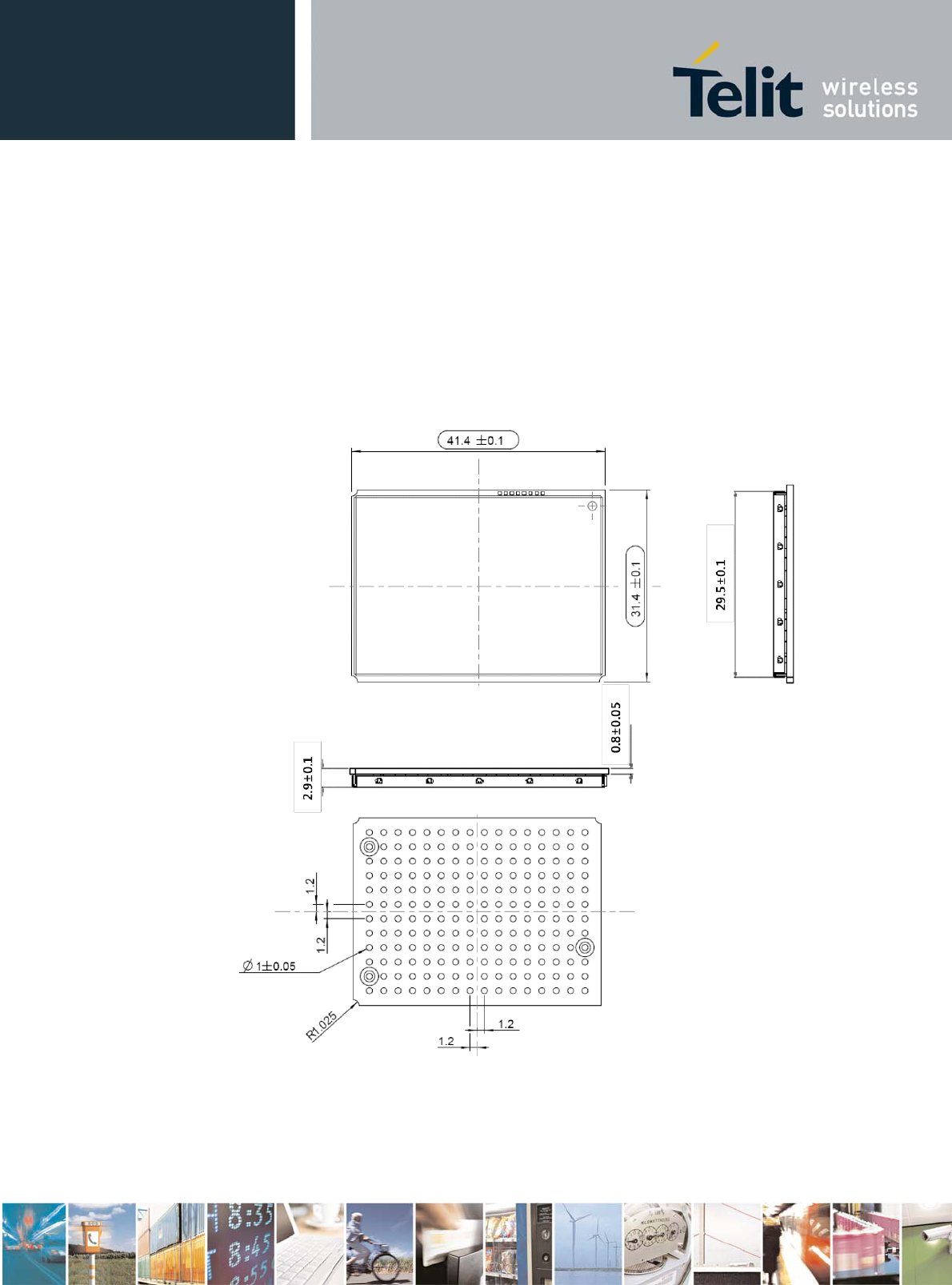
3. HE863 Family Mechanical Dimensions
The Telit HE863 Family module overall dimensions are:
• Length: 41.4 mm
• Width: 31.4 mm
• Thickness: 2.9 mm
HE863 Family Hardware User Guide
1vv0300891 Rev.5- 2011-03-18
Reproduction forbidden without Telit Communications S.p.A’s. written authorization - All Rights
Reserved. Page 15 of 89
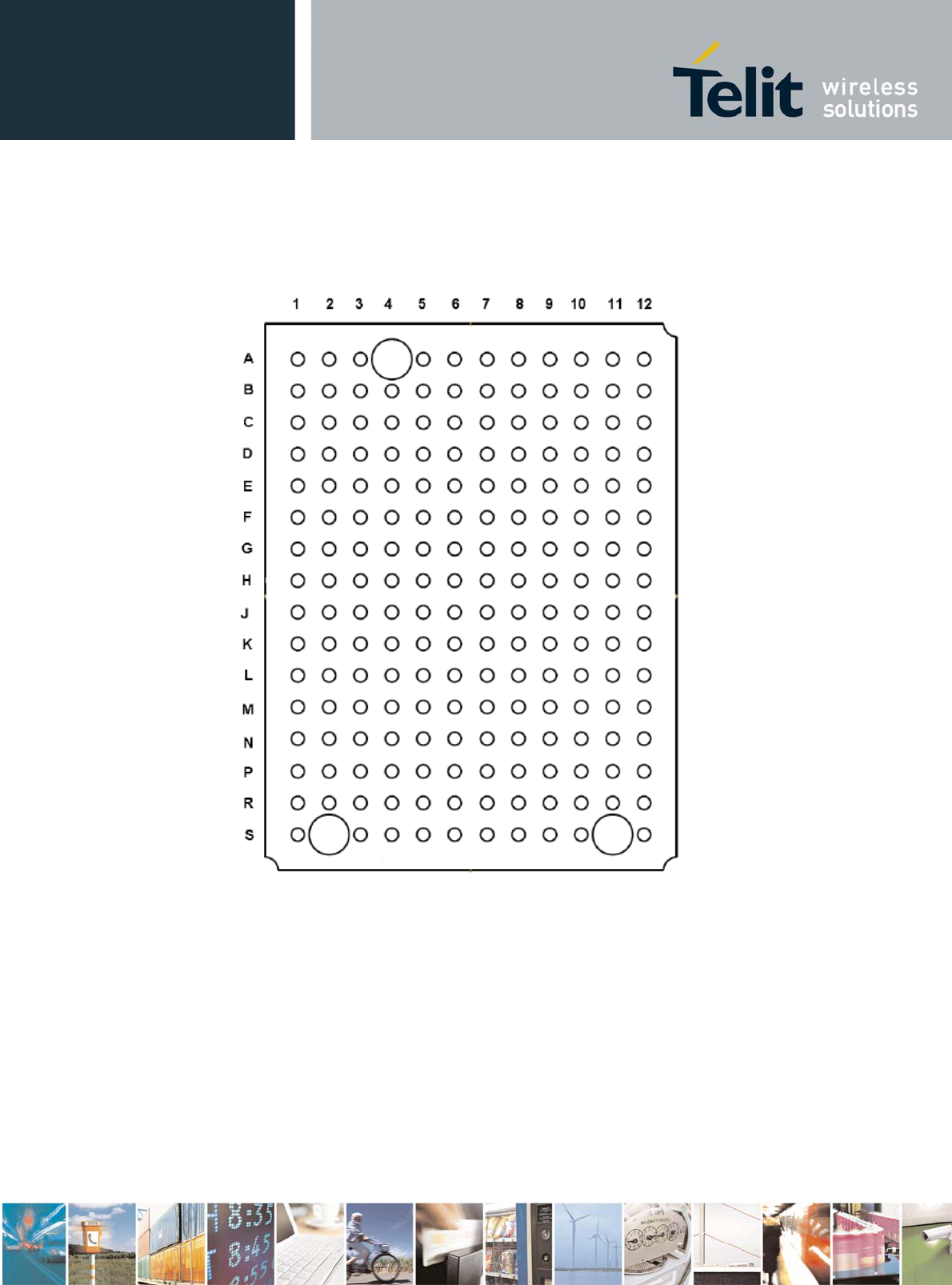
4. HE863 Family Module Connections
The HE863 Family features a 189 Balls Grid Array: in the following
sections a description of the available signals and their position in
the balls layout is presented.
4.1. HE863-EUD/NAD/AUD PIN-OUT
Ball Signal I/O Function Internal
Pull up Type
SIM card interface
H11 SIMCLK O External SIM signal – Clock 1.8 / 3V
G12 SIMRST O External SIM signal – Reset 1.8 / 3V
F12 SIMIO I/O External SIM signal - Data I/O 1.8 / 3V
E12 SIMIN(TBD) I External SIM signal – Presence
(active low) 1.8
H12 SIMVCC - External SIM signal – Power
supply for the SIM 1.8 / 3V
USB SIM(RESERVED)
F11 USB_SIM_D+
(TBD) I/O USB SIM data (+), TBD 1.8V/3.0V
G11 USB_SIM_D-
(TBD) I/O USB SIM data (-), TBD 1.8V/3.0V
Trace
N4 TX_TRACE O Tx data for diagnostic monitor CMOS 1.8V
N3 RX_TRACE I Rx data for diagnostic monitor CMOS 1.8V
Prog. / Data + HW Flow Control
M4 C125/RING
(TBD) O
Output for Ring indicator
signal (RI) to DTE
CMOS 1.8V
M3 C109/DCD
(TBD) O Output for Data set ready
signal (DSR) to DTE CMOS 1.8V
L3 C108/DTR
(TBD) I Input for Data terminal ready
signal (DTR) from DTE CMOS 1.8V
L4 C107/DSR
(TBD) O Output for Data set ready
signal (DSR) to DTE CMOS 1.8V
HE863 Family Hardware User Guide
1vv0300891 Rev.5- 2011-03-18
Reproduction forbidden without Telit Communications S.p.A’s. written authorization - All Rights
Reserved. Page 16 of 89
Ball Signal I/O Function Internal
Pull up Type
K4 C106/CTS O Output for Clear to send signal
(CTS) to DTE CMOS 1.8V
K3 C105/RTS I Input for Request to send
signal (RTS) from DTE CMOS 1.8V
J4 C104/RXD O Serial data output to DTE CMOS 1.8V
J3 C103/TXD I Serial data input (TXD) from
DTE CMOS 1.8V
USB
S8 USB_VBUS Power supply for the internal
USB transceiver 5V
S9 USB_ID(TBD) AI
Analog input used to sense
whether a peripheral device is
connected.
Analog
R9 USB_D+ I/O USB differential Data (+) 3.3V
R8 USB_D- I/O USB differential Data (-) 3.3V
DAC and ADC
S4 DAC_OUT AO Digital/Analog converter output Analog
S5 ADC_IN3 AI Analog/Digital converter input
3/GPS ANT current detection Analog
R5 ADC_IN2 AI Analog/Digital converter input
2/GPS ANT voltage detection Analog
R4 ADC_IN1 AI Analog/Digital converter input
1/GPS ANT voltage detection Analog
Miscellaneous Functions
G5 RESET* I Reset input Pull up 2.3V
C9 VRTC_2V3 AO VRTC Backup capacitor Power
B11 STAT_LED O Status indicator LED CMOS 1.8V
G4 ON_OFF* I
Input command for switching
power ON or OFF (toggle
command)
Pull up 2.3V
D10 PWRMON O Power ON Monitor CMOS 1.8V
A3 RF_ANT - Antenna for GSM/WCDMA – 50 ohm RF
P7 MODEM_RDY
(TBD) O Indicates that the boot
sequence completed successfully CMOS 1.8V

HE863 Family Hardware User Guide
1vv0300891 Rev.5- 2011-03-18
Reproduction forbidden without Telit Communications S.p.A’s. written authorization - All Rights
Reserved. Page 17 of 89
Ball Signal I/O Function Internal
Pull up Type
R6 WAKEUP(TBD) O Wake up signal to exte
r
nal host
system CMOS 1.8V
P6 SLEEP(TBD) I Input for entering sleep mode CMOS 1.8V
S6 CALL_KEY(TBD
) I Input for make/answer a call
(toggle command) CMOS 1.8V
G6 EMG_PWR_OFF
(TBD) I Input for emergency power off Pull up CMOS 1.8V
N8 MODE1(TBD) Mode select 1(TBD)
N9 MODE2(TBD) Mode select 2(TBD)
SPI(TBD) 6 pins for SPI
(F4,D4,F5,E4,D5,C11)
E5 VAUX1 - Power output for external
accessories Power
GPIO
L11 TGPIO_22 I/O Configurable GPIO #22 CMOS 1.8V
K12 TGPIO_21 I/O Configurable GPIO #21 CMOS 1.8V
M11 TGPIO_20 I/O Configurable GPIO #20 CMOS 1.8V
P10 TGPIO_19 I/O Configurable GPIO #19 CMOS 1.8V
M9 TGPIO_18 I/O Configurable GPIO #18 CMOS 1.8V
M7 TGPIO_17 I/O Configurable GPIO #17 CMOS 1.8V
N10 TGPIO_16 I/O Configurable GPIO #16 CMOS 1.8V
M12 TGPIO_15 I/O Configurable GPIO #15 CMOS 1.8V
P11 TGPIO_14 I/O Configurable GPIO #14 CMOS 1.8V
N11 TGPIO_13 I/O Configurable GPIO #13 CMOS 1.8V
L12 TGPIO_12 I/O Configurable GPIO #12 CMOS 1.8V
P12 TGPIO_11 I/O Configurable GPIO #11 CMOS 1.8V
M8 TGPIO_10 I/O Configurable GPIO #10 CMOS 1.8V
N12 TGPIO_09 I/O Configurable GPIO #09 CMOS 1.8V
B10 TGPIO_08 I/O Configurable GPIO #08 CMOS 1.8V
E9 TGPIO_07 I/O Configurable GPIO #07 CMOS 1.8V
E10 TGPIO_06
/ ALARM I/O
Configurable GPIO #06
/ ALARM CMOS 1.8V
HE863 Family Hardware User Guide
1vv0300891 Rev.5- 2011-03-18
Reproduction forbidden without Telit Communications S.p.A’s. written authorization - All Rights
Reserved. Page 18 of 89
Ball Signal I/O Function Internal
Pull up Type
F10 TGPIO_05 I/O Configurable GPIO #05 CMOS 1.8V
F9 TGPIO_04 I/O Configurable GPIO #04 CMOS 1.8V
K11 TGPIO_03 I/O Configurable GPIO #03 CMOS 1.8V
G9 TGPIO_02 I/O Configurable GPIO #02 CMOS 1.8V
J11 TGPIO_01 I/O Configurable GPIO #01 CMOS 1.8V
Power Supply
C1 VBATT Main power supply Power
D1 VBATT Main power supply Power
GND
52 pins for Ground
(A2,A5,A12,B2,B3,B4,B5,B9,C2,
C10,D6,D9,E1,E6,E11,F1,F6,G10,
H5,H6,H7,H8,H9,H10,J5,J10,J12,
K5,K10,L5,L6,L7,L8,L9,L10,M2,
M5,M10,N6,N7,P8,P9,R1,R2,R3,
R7,R10,R11,R12,S3,S7,S10)
Power
Reserved
RESERVED 9 pins reserved
(J8,J7,J6,K9,K8,K7,K6,N5,M6)
RESERVED
20 pins reserved
(D3,E3,F3,G3,H3,D2,E2,F2,C4,C3,
H2,J2,G2,K2,L1,K1,G1,J1,L2,H1)
RESERVED 7 pins reserved
(P5,P3,P2,M1,N1,N2,P1)
RESERVED 9 pins reserved
(G7,E7,D7,D8,E8,F8,G8,D11,F7)
RESERVED 6 pins reserved
(C5,B8,C7,C8,B7,C6)
RESERVED
17 pins reserved
(A7,A8,C12,J9,A1,A6,A9,A10,A11,
B1,B6,B12,D12,H4,P4,S1,S12)

HE863 Family Hardware User Guide
1vv0300891 Rev.5- 2011-03-18
Reproduction forbidden without Telit Communications S.p.A’s. written authorization - All Rights
Reserved. Page 19 of 89
NOTE:
RESERVED Pins must be UNCONNECTED BUT BE SOLDERED.
NOTE:
If not used, almost all pins must be left disconnected.

HE863 Family Hardware User Guide
1vv0300891 Rev.5- 2011-03-18
Reproduction forbidden without Telit Communications S.p.A’s. written authorization - All Rights
Reserved. Page 20 of 89
4.2. HE863-EUR/NAR PIN-OUT
Ball Signal I/O Function Internal
Pull up Type
Audio
J6 EAR_MT+ AO Earphone signal output, phase + Audio
J7 EAR_MT- AO Earphone signal output, phase - Audio
J8 EAR_HF+ AO Handsfree signal output, phase
+ (Single ended) Audio
K6 MIC_MT+ AI Mic signal input, phase + Audio
K7 MIC_MT- AI Mic signal input, phase - Audio
K8 MIC_HF+ AI Handsfree mic signal input,
phase + Audio
K9 MIC_HF- AI Handsfree mic signal input,
phase - Audio
PCM interface
M7 TGPIO_17/
PCM_SYNC I/O
GPIO 17/PCM sync signal of
digital voice interface CMOS 1.8V
M6 PCM_CLOCK I/O
PCM clock of digital voice
interface CMOS 1.8V
M8 TGPIO_10/
PCM_TX I/O
PCM data output of digital
voice interface CMOS 1.8V
M9 TGPIO_18/
PCM_RX I/O
PCM data input of digital voice
interface CMOS 1.8V
SIM card interface
H11 SIMCLK O External SIM signal – Clock 1.8 / 3V
G12 SIMRST O External SIM signal – Reset 1.8 / 3V
F12 SIMIO I/O External SIM signal - Data I/O 1.8 / 3V
E12 SIMIN(TBD) I External SIM signal – Presence
(active low) 1.8
H12 SIMVCC - External SIM signal – Power
supply for the SIM 1.8 / 3V
USB SIM(TBD)
F11 USB_SIM_D+
(TBD) I/O USB SIM data (+), TBD 1.8V/3.0V

HE863 Family Hardware User Guide
1vv0300891 Rev.5- 2011-03-18
Reproduction forbidden without Telit Communications S.p.A’s. written authorization - All Rights
Reserved. Page 21 of 89
Ball Signal I/O Function Internal
Pull up Type
G11 USB_SIM_D-
(TBD) I/O USB SIM data (-), TBD 1.8V/3.0V
Trace
N4 TX_TRACE O Tx data for diagnostic monitor CMOS 1.8V
N3 RX_TRACE I Rx data for diagnostic monitor CMOS 1.8V
Prog. / Data + HW Flow Control
M4 C125/RING
(TBD) O
Output for Ring indicator
signal (RI) to DTE
CMOS 1.8V
M3 C109/DCD
(TBD) O Output for Data set ready
signal (DSR) to DTE CMOS 1.8V
L3 C108/DTR
(TBD) I Input for Data terminal ready
signal (DTR) from DTE CMOS 1.8V
L4 C107/DSR
(TBD) O Output for Data set ready
signal (DSR) to DTE CMOS 1.8V
K4 C106/CTS O Output for Clear to send signal
(CTS) to DTE CMOS 1.8V
K3 C105/RTS I Input for Request to send
signal (RTS) from DTE CMOS 1.8V
J4 C104/RXD O Serial data output to DTE CMOS 1.8V
J3 C103/TXD I Serial data input (TXD) from
DTE CMOS 1.8V
USB
S8 USB_VBUS Power supply for the internal
USB transceiver 5V
S9 USB_ID(TBD) AI
Analog input used to sense
whether a peripheral device is
connected.
Analog
R9 USB_D+ I/O USB differential Data (+) 3.3V
R8 USB_D- I/O USB differential Data (-) 3.3V
DAC and ADC
S4 DAC_OUT AO Digital/Analog converter output Analog
S5 ADC_IN3 AI Analog/Digital converter input
3/GPS ANT current detection Analog

HE863 Family Hardware User Guide
1vv0300891 Rev.5- 2011-03-18
Reproduction forbidden without Telit Communications S.p.A’s. written authorization - All Rights
Reserved. Page 22 of 89
Ball Signal I/O Function Internal
Pull up Type
R5 ADC_IN2 AI Analog/Digital converter input
2/GPS ANT voltage detection Analog
R4 ADC_IN1 AI Analog/Digital converter input
1/GPS ANT voltage detection Analog
Miscellaneous Functions
G5 RESET* I Reset input Pull up 2.3V
C9 VRTC_2V3 AO VRTC Backup capacitor Power
B11 STAT_LED O Status indicator LED CMOS 1.8V
G4 ON_OFF* I
Input command for switching
power ON or OFF (toggle
command)
Pull up 2.3V
D10 PWRMON O Power ON Monitor CMOS 1.8V
A3 RF_ANT - Antenna for GSM/WCDMA – 50 ohm RF
P7 MODEM_RDY
(TBD) O Indicates that the boot
sequence completed successfully CMOS 1.8V
R6 WAKEUP(TBD) O Wake up signal to external host
system CMOS 1.8V
P6 SLEEP(TBD) I Input for entering sleep mode CMOS 1.8V
S6 CALL_KEY(TBD
) I Input for make/answer a call
(toggle command) CMOS 1.8V
N5 AXE(TBD) I Input for handsfree switching CMOS 1.8V
G6 EMG_PWR_OFF
(TBD) I Input for emergency power off Pull up CMOS 1.8V
N8 MODE1(TBD) Mode select 1(TBD)
N9 MODE2(TBD) Mode select 2(TBD)
SPI(TBD) 6 pins for SPI
(F4,D4,F5,E4,D5,C11)
E5 VAUX1 - Power output for external
accessories Power
GPIO
L11 TGPIO_22 I/O Configurable GPIO #22 CMOS 1.8V
K12 TGPIO_21 I/O Configurable GPIO #21 CMOS 1.8V
M11 TGPIO_20 I/O Configurable GPIO #20 CMOS 1.8V

HE863 Family Hardware User Guide
1vv0300891 Rev.5- 2011-03-18
Reproduction forbidden without Telit Communications S.p.A’s. written authorization - All Rights
Reserved. Page 23 of 89
Ball Signal I/O Function Internal
Pull up Type
P10 TGPIO_19 I/O Configurable GPIO #19 CMOS 1.8V
N10 TGPIO_16 I/O Configurable GPIO #16 CMOS 1.8V
M12 TGPIO_15 I/O Configurable GPIO #15 CMOS 1.8V
P11 TGPIO_14 I/O Configurable GPIO #14 CMOS 1.8V
N11 TGPIO_13 I/O Configurable GPIO #13 CMOS 1.8V
L12 TGPIO_12 I/O Configurable GPIO #12 CMOS 1.8V
P12 TGPIO_11 I/O Configurable GPIO #11 CMOS 1.8V
N12 TGPIO_09 I/O Configurable GPIO #09 CMOS 1.8V
B10 TGPIO_08 I/O Configurable GPIO #08 CMOS 1.8V
E9 TGPIO_07 I/O Configurable GPIO #07 CMOS 1.8V
E10 TGPIO_06
/ ALARM I/O
Configurable GPIO #06
/ ALARM CMOS 1.8V
F10 TGPIO_05 I/O Configurable GPIO #05 CMOS 1.8V
F9 TGPIO_04 I/O Configurable GPIO #04 CMOS 1.8V
K11 TGPIO_03 I/O Configurable GPIO #03 CMOS 1.8V
G9 TGPIO_02 I/O Configurable GPIO #02 CMOS 1.8V
J11 TGPIO_01 I/O Configurable GPIO #01 CMOS 1.8V
Power Supply
C1 VBATT Main power supply Power
D1 VBATT Main power supply Power
GND
52 pins for Ground
(A2,A5,A12,B2,B3,B4,B5,B9,C2,
C10,D6,D9,E1,E6,E11,F1,F6,G10,
H5,H6,H7,H8,H9,H10,J5,J10,J12,
K5,K10,L5,L6,L7,L8,L9,L10,M2,
M5,M10,N6,N7,P8,P9,R1,R2,R3,
R7,R10,R11,R12,S3,S7,S10)
Power
Reserved
RESERVED
20 pins reserved
(D3,E3,F3,G3,H3,D2,E2,F2,C4,C3,
H2,J2,G2,K2,L1,K1,G1,J1,L2,H1)
RESERVED 7 pins reserved
(P5,P3,P2,M1,N1,N2,P1)
HE863 Family Hardware User Guide
1vv0300891 Rev.5- 2011-03-18
Reproduction forbidden without Telit Communications S.p.A’s. written authorization - All Rights
Reserved. Page 24 of 89
Ball Signal I/O Function Internal
Pull up Type
RESERVED 9 pins reserved
(G7,E7,D7,D8,E8,F8,G8,D11,F7)
RESERVED 6 pins reserved
(C5,B8,C7,C8,B7,C6)
RESERVED
17 pins reserved
(A7,A8,C12,J9,A1,A6,A9,A10,A11,
B1,B6,B12,D12,H4,P4,S1,S12)
NOTE:
RESERVED Pins must be UNCONNECTED but be soldered.
NOTE:
If not used, almost all pins must be left disconnected.

HE863 Family Hardware User Guide
1vv0300891 Rev.5- 2011-03-18
Reproduction forbidden without Telit Communications S.p.A’s. written authorization - All Rights
Reserved. Page 25 of 89
4.3. HE863-EUG/NAG/AUG PIN-OUT
Ball Signal I/O Function Internal
Pull up Type
Audio
J6 EAR_MT+ AO Earphone signal output, phase + Audio
J7 EAR_MT- AO Earphone signal output, phase - Audio
J8 EAR_HF+ AO Handsfree signal output, phase
+ (Single ended) Audio
K6 MIC_MT+ AI Mic signal input, phase + Audio
K7 MIC_MT- AI Mic signal input, phase - Audio
K8 MIC_HF+ AI Handsfree mic signal input,
phase + Audio
K9 MIC_HF- AI Handsfree mic signal input,
phase - Audio
PCM interface
M7 TGPIO_17/
PCM_SYNC I/O
GPIO 17/PCM sync signal of
digital voice interface CMOS 1.8V
M6 PCM_CLOCK I/O
PCM clock of digital voice
interface CMOS 1.8V
M8 TGPIO_10/
PCM_TX I/O
PCM data output of digital
voice interface CMOS 1.8V
M9 TGPIO_18/
PCM_RX I/O
PCM data input of digital
v
oice
interface CMOS 1.8V
SIM card interface
H11 SIMCLK O External SIM signal – Clock 1.8 / 3V
G12 SIMRST O External SIM signal – Reset 1.8 / 3V
F12 SIMIO I/O External SIM signal - Data I/O 1.8 / 3V
E12 SIMIN(TBD) I External SIM signal – Presence
(active low) 1.8
H12 SIMVCC - External SIM signal – Power
supply for the SIM 1.8 / 3V
USB SIM(TBD)
F11 USB_SIM_D+
(TBD) I/O USB SIM data (+), TBD 1.8V/3.0V
G11 USB_SIM_D- I/O USB SIM data (-), TBD 1.8V/3.0V

HE863 Family Hardware User Guide
1vv0300891 Rev.5- 2011-03-18
Reproduction forbidden without Telit Communications S.p.A’s. written authorization - All Rights
Reserved. Page 26 of 89
Ball Signal I/O Function Internal
Pull up Type
(TBD)
Trace
N4 TX_TRACE O Tx data for diagnostic monitor CMOS 1.8V
N3 RX_TRACE I Rx data for diagnostic monitor CMOS 1.8V
Prog. / Data + HW Flow Control
M4 C125/RING
(TBD) O
Output for Ring indicator
signal (RI) to DTE
CMOS 1.8V
M3 C109/DCD
(TBD) O Output for Data set ready
signal (DSR) to DTE CMOS 1.8V
L3 C108/DTR
(TBD) I Input for Data terminal ready
signal (DTR) from DTE CMOS 1.8V
L4 C107/DSR
(TBD) O Output for Data set ready
signal (DSR) to DTE CMOS 1.8V
K4 C106/CTS O Output for Clear to send signal
(CTS) to DTE CMOS 1.8V
K3 C105/RTS I Input for Request to send
signal (RTS) from DTE CMOS 1.8V
J4 C104/RXD O Serial data output to DTE CMOS 1.8V
J3 C103/TXD I Serial data input (TXD) from
DTE CMOS 1.8V
USB
S8 USB_VBUS Power supply for the internal
USB transceiver 5V
S9 USB_ID(TBD) AI
Analog input used to sense
whether a peripheral device is
connected.
Analog
R9 USB_D+ I/O USB differential Data (+) 3.3V
R8 USB_D- I/O USB differential Data (-) 3.3V
DAC and ADC
S4 DAC_OUT AO Digital/Analog converter output Analog
S5 ADC_IN3 AI Analog/Digital converter input
3/GPS ANT current detection Analog
R5 ADC_IN2 AI Analog/Digital converter input Analog
HE863 Family Hardware User Guide
1vv0300891 Rev.5- 2011-03-18
Reproduction forbidden without Telit Communications S.p.A’s. written authorization - All Rights
Reserved. Page 27 of 89
Ball Signal I/O Function Internal
Pull up Type
2/GPS ANT voltage detection
R4 ADC_IN1 AI Analog/Digital converter input
1/GPS ANT voltage detection Analog
Miscellaneous Functions
G5 RESET* I Reset input Pull up 2.3V
C9 VRTC_2V3 AO VRTC Backup capacitor Power
B11 STAT_LED O Status indicator LED CMOS 1.8V
G4 ON_OFF* I
Input command for switching
power ON or OFF (toggle
command)
Pull up 2.3V
D10 PWRMON O Power ON Monitor CMOS 1.8V
A3 RF_ANT - Antenna for GSM/WCDMA – 50 ohm RF
S1 GPS_ANT -
Antenna for GPS – 50 ohm
GPS_ANT for HE863-EUG/NAG/AUG
only
RF
P7 MODEM_RDY
(TBD) O Indicates that the boot
sequence completed successfully CMOS 1.8V
R6 WAKEUP(TBD) O Wake u
p
signal to external host
system CMOS 1.8V
P6 SLEEP(TBD) I Input for entering sleep mode CMOS 1.8V
S6 CALL_KEY(TBD
) I Input for make/answer a call
(toggle command) CMOS 1.8V
N5 AXE
(TBD) I Input for handsfree switching CMOS 1.8V
G6 EMG_PWR_OFF
(TBD) I Input for emergency power off Pull up CMOS 1.8V
N8 MODE1(TBD) Mode select 1(TBD)
N9 MODE2(TBD) Mode select 2(TBD)
SPI(TBD) 6 pins for SPI
(F4,D4,F5,E4,D5,C11)
E5 VAUX1 - Power output for external
accessories Power
GPIO
HE863 Family Hardware User Guide
1vv0300891 Rev.5- 2011-03-18
Reproduction forbidden without Telit Communications S.p.A’s. written authorization - All Rights
Reserved. Page 28 of 89
Ball Signal I/O Function Internal
Pull up Type
L11 TGPIO_22 I/O Configurable GPIO #22 CMOS 1.8V
K12 TGPIO_21 I/O Configurable GPIO #21 CMOS 1.8V
M11 TGPIO_20 I/O Configurable GPIO #20 CMOS 1.8V
P10 TGPIO_19 I/O Configurable GPIO #19 CMOS 1.8V
N10 TGPIO_16 I/O Configurable GPIO #16 CMOS 1.8V
M12 TGPIO_15 I/O Configurable GPIO #15 CMOS 1.8V
P11 TGPIO_14 I/O Configurable GPIO #14 CMOS 1.8V
N11 TGPIO_13 I/O Configurable GPIO #13 CMOS 1.8V
L12 TGPIO_12 I/O Configurable GPIO #12 CMOS 1.8V
P12 TGPIO_11 I/O Configurable GPIO #11 CMOS 1.8V
N12 TGPIO_09 I/O Configurable GPIO #09 CMOS 1.8V
B10 TGPIO_08 I/O Configurable GPIO #08 CMOS 1.8V
E9 TGPIO_07 I/O Configurable GPIO #07 CMOS 1.8V
E10 TGPIO_06
/ ALARM I/O
Configurable GPIO #06
/ ALARM CMOS 1.8V
F10 TGPIO_05 I/O Configurable GPIO #05 CMOS 1.8V
F9 TGPIO_04 I/O Configurable GPIO #04 CMOS 1.8V
K11 TGPIO_03 I/O Configurable GPIO #03 CMOS 1.8V
G9 TGPIO_02 I/O Configurable GPIO #02 CMOS 1.8V
J11 TGPIO_01 I/O Configurable GPIO #01 CMOS 1.8V
Power Supply
C1 VBATT Main power supply Power
D1 VBATT Main power supply Power
GND
52 pins for Ground
(A2,A5,A12,B2,B3,B4,B5,B9,C2,
C10,D6,D9,E1,E6,E11,F1,F6,G10,
H5,H6,H7,H8,H9,H10,J5,J10,J12,
K5,K10,L5,L6,L7,L8,L9,L10,M2,
M5,M10,N6,N7,P8,P9,R1,R2,R3,
R7,R10,R11,R12,S3,S7,S10)
Power
HE863 Family Hardware User Guide
1vv0300891 Rev.5- 2011-03-18
Reproduction forbidden without Telit Communications S.p.A’s. written authorization - All Rights
Reserved. Page 29 of 89
Ball Signal I/O Function Internal
Pull up Type
Reserved
RESERVED
20 pins reserved
(D3,E3,F3,G3,H3,D2,E2,F2,C4,C3,
H2,J2,G2,K2,L1,K1,G1,J1,L2,H1)
RESERVED 7 pins reserved
(P5,P3,P2,M1,N1,N2,P1)
RESERVED 9 pins reserved
(G7,E7,D7,D8,E8,F8,G8,D11,F7)
RESERVED 6 pins reserved
(C5,B8,C7,C8,B7,C6)
RESERVED
16 pins reserved
(A7,A8,C12,J9,A1,A6,A9,A10,A11,
B1,B6,B12,D12,H4,P4,S12)
NOTE:
RESERVED Pins must be UNCONNECTED but be soldered.
NOTE:
If not used, almost all pins must be left disconnected.
HE863 Family Hardware User Guide
1vv0300891 Rev.5- 2011-03-18
Reproduction forbidden without Telit Communications S.p.A’s. written authorization - All Rights
Reserved. Page 30 of 89
4.4. BALLS LAYOUT
TOP VIEW
HE863 Family Hardware User Guide
1vv0300891 Rev.5- 2011-03-18
Reproduction forbidden without Telit Communications S.p.A’s. written authorization - All Rights
Reserved. Page 31 of 89
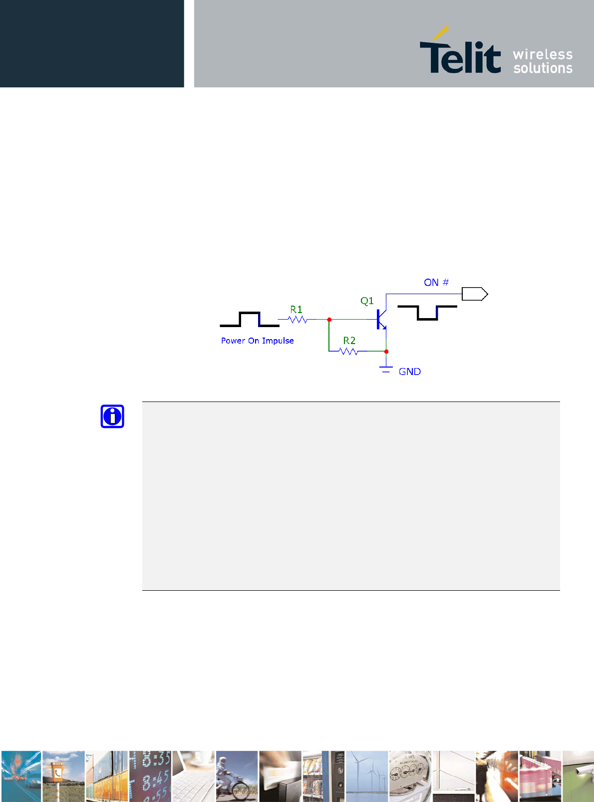
5. Hardware Commands
5.1. Turning ON the HE863
To turn on HE863 Family, the pad ON/OFF# must be tied low for
at least 1 second and then released.
The maximum current that can be drained from the ON/OFF# pad
is 0.1 mA.
A simple circuit to do it is:
NOTE:
The HE863 Family turns fully on by supplying power more than
3.2V to the VBATT pads because of the first connect power on
feature. This feature could be done only when Vbatt equals to
almost 0V at the beginning. Normally the high value capacitor
will be mounted on Vbatt line so the user should have a wait
enoughly since vbatt is disabled till the remaining voltage on
Vbatt is fully dischaged in order to do re-start by this
feature.
Because the discharge time depends upon the capacitance on
Vbatt in the application it should be definitely considered in
the application side.
HE863 Family has dozens uF on Vbatt line inside.
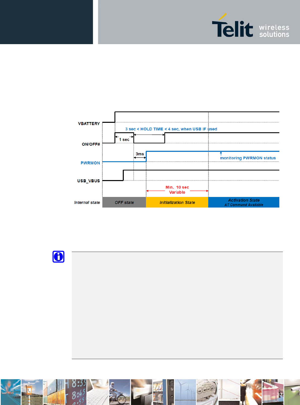
5.2. Initialization and Activation state
Upon turning on HE863 Family, HE863 Family is not activated
yet because the boot sequence of HE863 Family is still going
on internally. It may take more than about 10 seconds to
complete the initializing the module internally.
For this reason, it would be useless to try to access HE863
Family during Initialization state as below. To get the
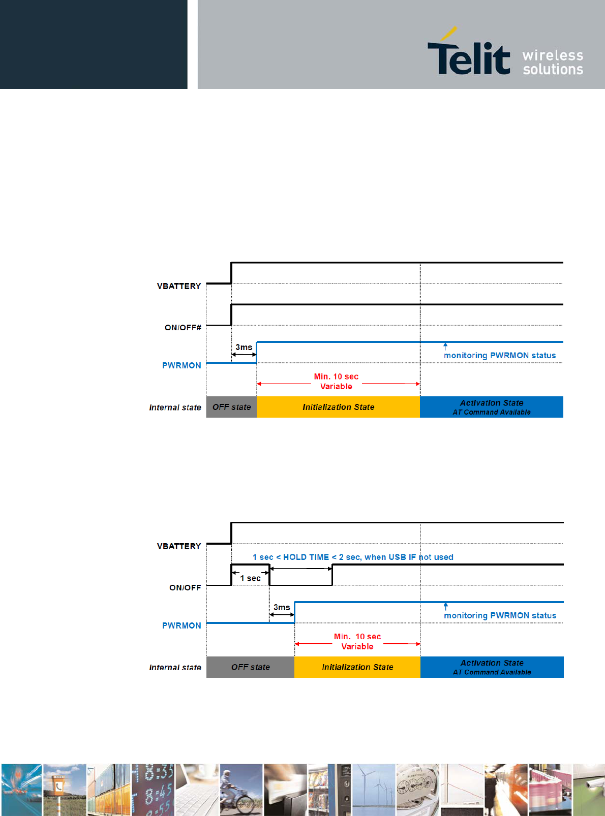
HE863 Family Hardware User Guide
1vv0300891 Rev.5- 2011-03-18
Reproduction forbidden without Telit Communications S.p.A’s. written authorization - All Rights
Reserved. Page 32 of 89
desirable stability, HE863 Family needs at least 10 seconds
after the PWRMON goes High.
Following time charts can be referred according to the
application design.
i. First time supplying the power more than 3.2V to Vbatt
By only first time supplying the power to Vbatt line, the
HE863 Family will power on without toggling ON/OFF# pin.
ii. Using ON/OFF key when USB interface is not used
If the application will not use the usb interface of HE863
Family, that is, actually the usb interface is not connected
between the devices, the hold time to tie ON/OFF# to GND
should be 1 ~ 2 sec to make it powering on.
HE863 Family Hardware User Guide
1vv0300891 Rev.5- 2011-03-18
Reproduction forbidden without Telit Communications S.p.A’s. written authorization - All Rights
Reserved. Page 33 of 89
iii. Using ON/OFF key when USB interface is used
If the application will use the usb interface of HE863 Family,
that is, actually the usb interface is correctly connected
between the devices and USB_VBUS is asserted, the hold time to
tie ON/OFF# to GND should be 3 ~ 4 sec to make it powering on.
During the Initialization state, any kind of AT-command is not
available. DTE must be waiting for the Activation state to
communicate with HE863 Family.
NOTE:
To check if the HE863 Family has powered on, the hardware line
PWRMON must be monitored. When PWRMON goes high, the module
has powered on.
NOTE:
Do not use any pull up resistor on the ON/OFF# line, it is
internally pulled up. Using pull up resistor may bring to
latch up problems on the HE863 Family power regulator and
improper power on/off of the module. The line ON# must be
connected only in open collector configuration.
NOTE:
In this document all the lines are inverted. Active low
signals are labeled with a name that ends with a "#" or with a
bar over the name.
HE863 Family Hardware User Guide
1vv0300891 Rev.5- 2011-03-18
Reproduction forbidden without Telit Communications S.p.A’s. written authorization - All Rights
Reserved. Page 34 of 89
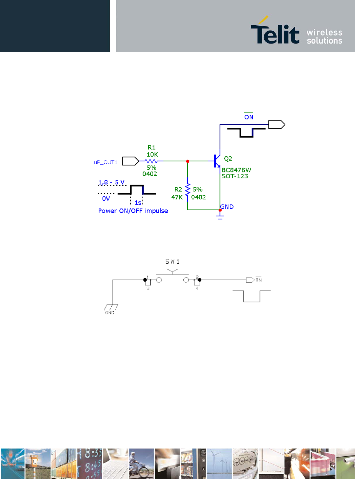
For example:
1- Let us assume you need to drive the ON/OFF# pad with a totem
pole output of a +1.8/5 V microcontroller (uP_OUT1):
2- Let us assume you need to drive the ON/OFF# pad directly
with an ON/OFF button:
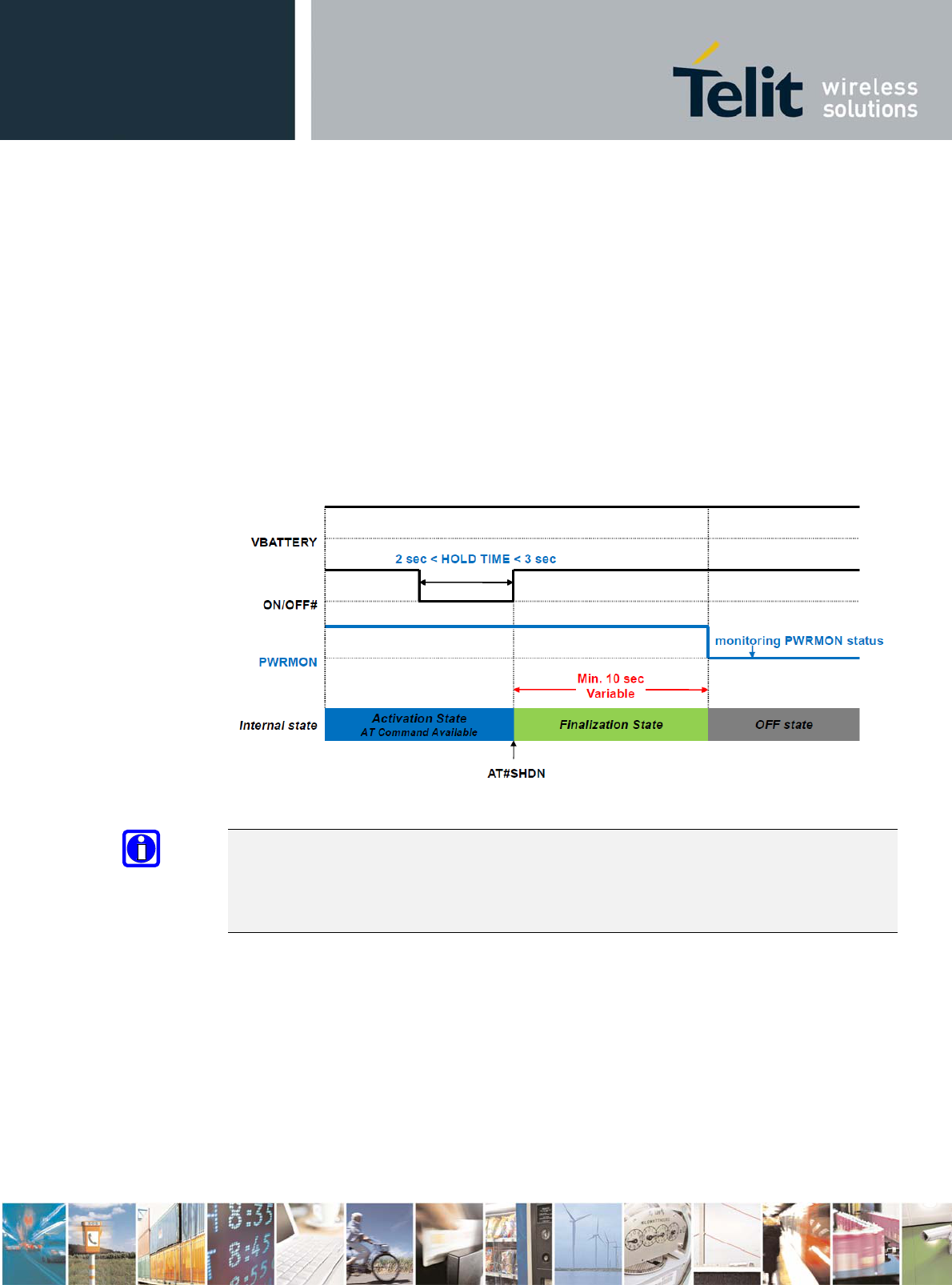
5.3. Turning OFF the HE863
The turning off the device can be done by below ways:
- via AT command only (see HE863 Software User Guide)
- by tying low the ON/OFF# pad for at least 2 seconds.
Either ways the device issues to the network a detach request
that informs the network that the device will not be reachable
any more.
To turn OFF HE863 Family the pad ON/OFF# must be tied low for
at least 2 seconds and then released.
HE863 Family Hardware User Guide
1vv0300891 Rev.5- 2011-03-18
Reproduction forbidden without Telit Communications S.p.A’s. written authorization - All Rights
Reserved. Page 35 of 89
When the hold time of ON/OFF# reaches above 2 seconds, HE863
Family goes into the finalization state and finally will shut
down PWRMON at the end of this state.
The period of the finalization state can differ from the
situation in which the HE863 Family is so it cannot be fixed
definitely.
Normally it will take above 10 seconds later from releasing
ON/OFF# and DTE should monitor the status of PWRMON to see the
actual power off.
TIP:
To check if the device has powered off, hardware line PWRMON
must be monitored. When PWRMON goes low it can be considered
the device has powered off.
HE863 Family Hardware User Guide
1vv0300891 Rev.5- 2011-03-18
Reproduction forbidden without Telit Communications S.p.A’s. written authorization - All Rights
Reserved. Page 36 of 89
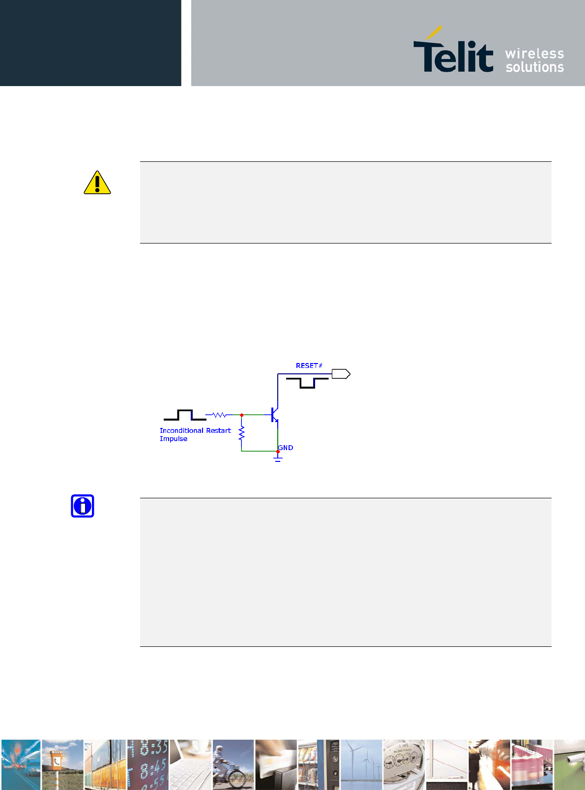
5.3.1. Hardware Unconditional Restart
WARNING:
The hardware unconditional Restart must not be used during
normal operation of the device since it does not detach the
device from the network. It shall be kept as an emergency exit
procedure to be done in the rare case that the device gets
stacked waiting for some network or SIM responses.
To unconditionally restart the HE863 Family, the pad RESET#
must be tied low for at least 200 milliseconds and then
released.
A simple circuit to do it is:
NOTE:
Do not use any pull up resistor on the RESET# line or any
totem pole digital output. Using pull up resistor may bring to
latch up problems on the HE863 Family power regulator and
improper functioning of the module. The line RESET# must be
connected only in open collector configuration
TIP:
The unconditional hardware Restart must always be implemented
on the boards and the software must use it as an emergency
exit procedure.
HE863 Family Hardware User Guide
1vv0300891 Rev.5- 2011-03-18
Reproduction forbidden without Telit Communications S.p.A’s. written authorization - All Rights
Reserved. Page 37 of 89
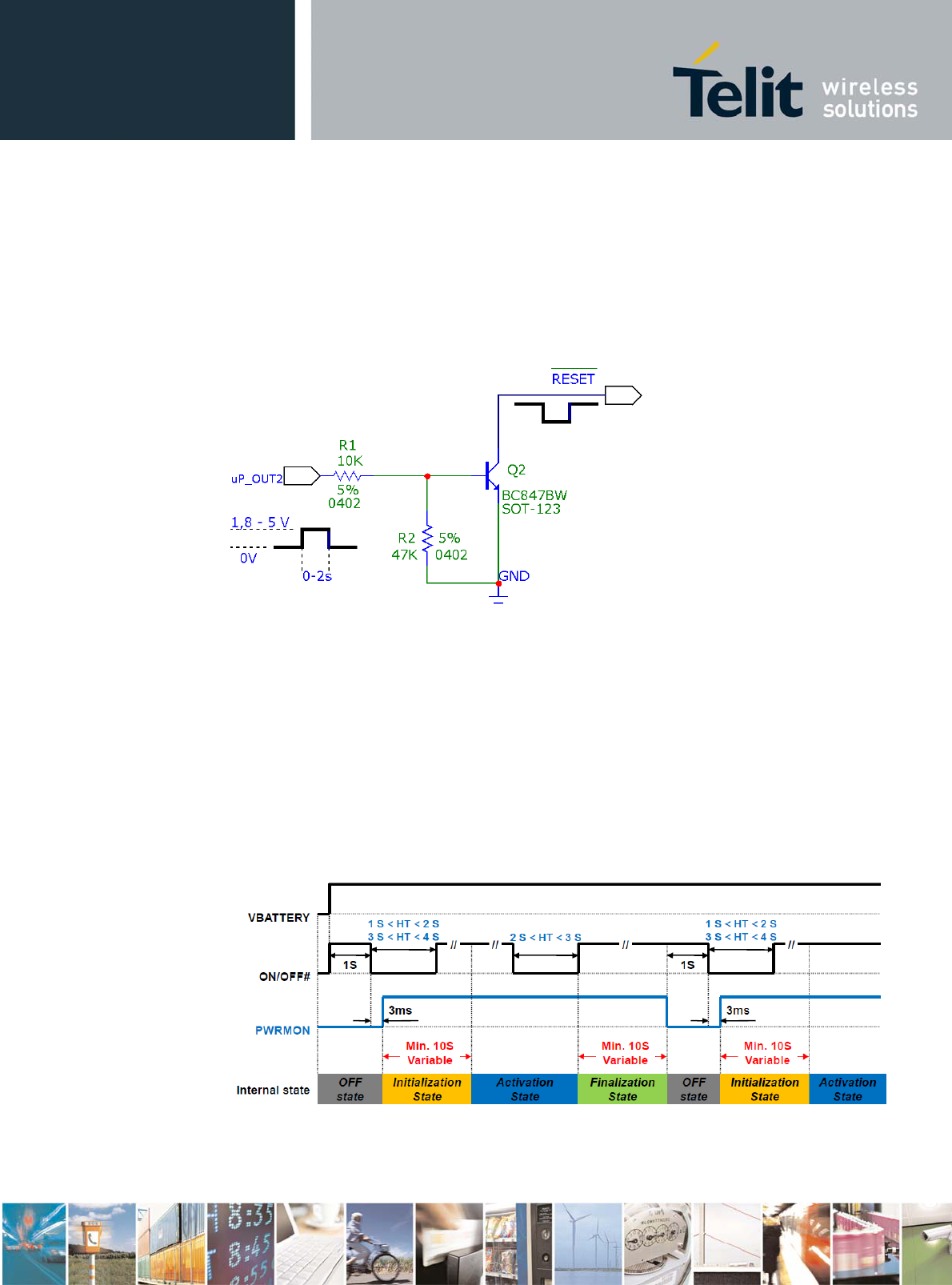
For example:
1- Let us assume you need to drive the RESET# pad with a totem
pole output of a +1.8/5 V microcontroller (uP_OUT2):
This signal is internally pulled up so the pin can be left
floating if not used.
5.4. Summary of Turning ON and OFF the HE863
Below chart describes the overall sequences for turning ON and
OFF.
HE863 Family Hardware User Guide
1vv0300891 Rev.5- 2011-03-18
Reproduction forbidden without Telit Communications S.p.A’s. written authorization - All Rights
Reserved. Page 38 of 89
6. Power Supply
The power supply circuitry and board layout are a very
important part in the full product design and they strongly
reflect on the product overall performances. Read carefully
the requirements and the guidelines that will follow for a
proper design.
6.1. Power Supply Requirements
The HE863 Family power requirements are:
Power Supply
Nominal Supply Voltage 3.8V
Max Supply Voltage 4.2V
Supply Voltage Range 3.4V – 4.2V
HE863-EUD/NAD/AUD/EUG/NAG/AUG/EUR/NAR
Mode Average(mA) Mode Description
IDLE mode Standby mode; no call in progress;
GPS OFF (GPS for HE863-EUG/NAG/AUG only)
AT+CFUN=0 - 60uA Shutdown mode(Power off)
AT+CFUN=1 WCDMA 34 Normal mode; full functionality of the
module
GSM 33
AT+CFUN=4 WCDMA 33 Disabled TX and RX; modules is not
registered on the network
GSM 33
AT+CFUN=5
WCDMA 4/2* CFN=5 full functionality with power
saving;
Module registered on the network can
receive incoming call and SMS
GSM 4/2*
WCDMA TX and RX mode with GPS OFF GPS OFF (GPS for HE863-EUG/NAG/AUG only)
WCDMA Voice 600 WCDMA voice channel
WCDMA data 600 WCDMA data channel
HSDPA 680 HSDPA data channel
HSUPA 610 HSUPA data channel
GSM TX and RX mode with GPS OFF GPS OFF (GPS for HE863-EUG/NAG/AUG only)
GSM Voice 250 GSM voice channel
GPRS Class12 650 GPRS data channel
EDGE Class12 470 EDGE data channel
* Worst/best case depends on network configuration and is not under
module control.
HE863 Family Hardware User Guide
1vv0300891 Rev.5- 2011-03-18
Reproduction forbidden without Telit Communications S.p.A’s. written authorization - All Rights
Reserved. Page 39 of 89
HE863-EUG/NAG/AUG only
Mode Average(mA) Mode Description
IDLE mode with GPS ON full power
mode*
Standby mode;
no call in progress;
GPS ON
AT+CFUN=1 WCDMA 62
GSM 61
AT+CFUN=4 WCDMA 61
GSM 61
AT+CFUN=5 WCDMA 54/53*
GSM 54/53*
WCDMA TX and RX mode with
G
PS ON
full power mode*
WCDMA Voice 630 WCDMA voice channel
WCDMA Data 630 WCDMA data channel
HSDPA 710 HSDPA data channel
HSUPA 630 HSUPA data channel
GSM TX and RX mode with GPS ON
full power mode*
GSM Voice 280 GSM voice channel
GPRS Class12 670 GPRS data channel
EDGE Class12 500 EDGE data channel
* except external active GPS antenna
TIP:
The electrical design for the Power supply must be made
ensuring that it will be capable of a peak current output of
at least 2A.
In GSM/GPRS mode, RF transmission is not continuous and it is
packed into bursts at a base frequency of about 216 Hz, and
the relative current peaks can be as high as about 2A.
Therefore the power supply has to be designed in order to
withstand these current peaks without big voltage drops; this
means that both the electrical design and the board layout
must be designed for this current flow. If the layout of the
PCB is not well designed, a strong noise floor is generated on
the ground; this will reflect on all the audio paths producing
an audible annoying noise at 216 Hz; if the voltage drops
during the peak, current absorption is too much. The device
may even shut down as a consequence of the supply voltage drop.

HE863 Family Hardware User Guide
1vv0300891 Rev.5- 2011-03-18
Reproduction forbidden without Telit Communications S.p.A’s. written authorization - All Rights
Reserved. Page 40 of 89
6.2. General Design Rules
The principal guidelines for the Power Supply Design embrace
three different design steps:
the electrical design
the thermal design
the PCB layout
6.2.1. Electrical Design Guidelines
The electrical design of the power supply depends strongly on
the power source where this power is drained. We will
distinguish them into two categories:
+5V input (typically PC internal regulator output)
+12V input (typically automotive)
6.2.1.1. + 5V Input Source Power Supply Design Guidelines
The desired output for the power supply is 3.8V, hence
there is not a big difference between the input source
and the desired output and a linear regulator can be
used. A switching power supply will not be suited
because of the low drop-out requirements.
When using a linear regulator, a proper heat sink must
be provided in order to dissipate the power generated.
A Bypass low ESR capacitor of adequate capacity must
be provided in order to cut the current absorption
peaks close to HE863 Family, a 100μF tantalum
capacitor is usually suited.
Make sure the low ESR capacitor on the power supply
output (usually a tantalum one) is rated at least 10V.
A protection diode must be inserted close to the power
input, in order to save HE863 Family from power
polarity inversion.

HE863 Family Hardware User Guide
1vv0300891 Rev.5- 2011-03-18
Reproduction forbidden without Telit Communications S.p.A’s. written authorization - All Rights
Reserved. Page 41 of 89
An example of linear regulator with 5V input is:
6.2.1.2. +12V Input Source Power Supply Design Guidelines
The desired output for the power supply is 3.8V, hence
due to the big difference between the input source and
the desired output, a linear regulator is not suited
and must not be used. A switching power supply will be
preferable because of its better efficiency especially
with the 2A peak current load represented by HE863
Family.
When using a switching regulator, a 500 kHz or more
switching frequency regulator is preferable because of
its smaller inductor size and its faster transient
response. This allows the regulator to respond quickly
to the current peaks absorption.
In any case, the frequency and Switching design
selection is related to the application to be
developed due to the fact the switching frequency
could also generate EMC interferences.
For car PB battery the input voltage can rise up to
15.8V and this must be kept in mind when choosing
components: all components in the power supply must
withstand this voltage.
A Bypass low ESR capacitor of adequate capacity must
be provided in order to cut the current absorption
peaks. A 100μF tantalum capacitor is usually suited
for this.
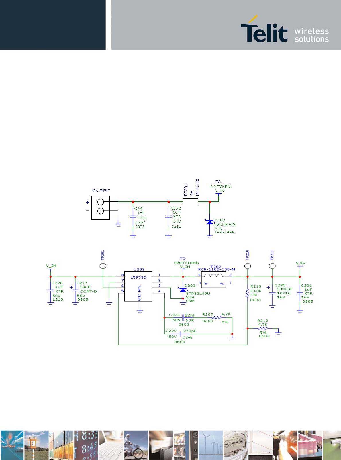
HE863 Family Hardware User Guide
1vv0300891 Rev.5- 2011-03-18
Reproduction forbidden without Telit Communications S.p.A’s. written authorization - All Rights
Reserved. Page 42 of 89
Make sure the low ESR capacitor on the power supply
output (usually a tantalum one) is rated at least 10V.
For Car applications a spike protection diode must be
inserted close to the power input, in order to clean
the supply from spikes.
A protection diode must be inserted close to the power
input, in order to save HE863 Family from power
polarity inversion. This can be the same diode as for
spike protection.
An example of switching regulator with 12V input is in the
below schematic (it is split in 2 parts):
Switching regulator
HE863 Family Hardware User Guide
1vv0300891 Rev.5- 2011-03-18
Reproduction forbidden without Telit Communications S.p.A’s. written authorization - All Rights
Reserved. Page 43 of 89
6.2.2. Thermal Design Guidelines
The thermal design for the power supply heat sink must be done
with the following specifications:
Average current consumption during WCDMA/HSPA
transmission @PWR level max : 710mA
Average current consumption during class12 GPRS
transmission @PWR level max : 670mA
Average GPS current during GPS ON (Power Saving
disabled) in HE863-EUG/NAG/AUG : 55mA
NOTE:
The average consumption during transmissions depends on the
power level at which the device is requested to transmit via
the network. The average current consumption hence varies
significantly.
NOTE:
The thermal design for the Power supply must be made keeping
an average consumption at the max transmitting level during
calls of 750mA rms plus 100mA rms for GPS in tracking mode in
HE863-EUG/NAG/AUG.
Considering the very low current during idle, especially if
Power Saving function is enabled, it is possible to consider
from the thermal point of view that the device absorbs current
significantly only during calls.
If we assume that the device stays in transmission for short
periods of time (let us say few minutes) and then remains for
quite a long time in idle (let us say one hour), then the
power supply has always the time to cool down between the
calls and the heat sink could be smaller than the calculated
for 850mA maximum RMS current. There could even be a simple
chip package (no heat sink).
Moreover in average network conditions the device is requested
to transmit at a lower power level than the maximum and hence
the current consumption will be less than 850mA (TBD, being
usually around 150mA).
For these reasons the thermal design is rarely a concern and
the simple ground plane where the power supply chip is placed
can be enough to ensure a good thermal condition and avoid
overheating.
For the heat generated by the HE863 Family, you can consider
it to be during transmission 1W max during CSD/VOICE calls and

HE863 Family Hardware User Guide
1vv0300891 Rev.5- 2011-03-18
Reproduction forbidden without Telit Communications S.p.A’s. written authorization - All Rights
Reserved. Page 44 of 89
2W max during class12 GPRS upload. This generated heat will
be mostly conducted to the ground plane under the HE863
Family; you must ensure that your application can dissipate
heat.
In the WCDMA/HSPA mode, since HE863 Family emits RF signals
continuously during transmission, you must pay special
attention how to dissipate the heat generated.
The current consumption will be up to about 710mA in HSPA
continuously at the maximum TX output power (23dBm). Thus, you
must arrange the PCB area as large as possible under HE863
Family which you will mount.
You must mount HE863 Family on the large ground area of your
application board and make many ground vias to dissipate the
heat.
The peak current consumption in the GSM mode is higher than
that in WCDMA. However, considering the heat sink is more
important in case of WCDMA.
As mentioned before, a GSM signal is bursty, thus, the
temperature drift is more insensible than WCDMA. Consequently,
if you prescribe the heat dissipation in the WCDMA mode, you
don’t need to think more about the GSM mode.
6.2.3. Power Supply PCB Layout Guidelines
As seen in the electrical design guidelines, the power supply
must have a low ESR capacitor on the output to cut the current
peaks and a protection diode on the input to protect the
supply from spikes and polarity inversion. The placement of
these components is crucial for the correct working of the
circuitry. A misplaced component can be useless or can even
decrease the power supply performances.
The Bypass low ESR capacitor must be placed close to
the Telit HE863 Family power input pads, or in the
case the power supply is a switching type, it can be
placed close to the inductor to cut the ripple if the
PCB trace from the capacitor to HE863 Family is wide
enough to ensure a drop-less connection even during
the 2A current peaks.
The protection diode must be placed close to the input
connector where the power source is drained.
The PCB traces from the input connector to the power
regulator. IC must be wide enough to ensure no voltage
drops to occur when the 2A current peaks are absorbed.

HE863 Family Hardware User Guide
1vv0300891 Rev.5- 2011-03-18
Reproduction forbidden without Telit Communications S.p.A’s. written authorization - All Rights
Reserved. Page 45 of 89
Note that this is not made in order to save power loss
but especially to avoid the voltage drops on the power
line at the current peaks frequency of 216 Hz that
will reflect on all the components connected to that
supply (also introducing the noise floor at the burst
base frequency.) For this reason while a voltage drop
of 300-400 mV may be acceptable from the power loss
point of view, the same voltage drop may not be
acceptable from the noise point of view. If your
application does not have audio interface but only
uses the data feature of the Telit HE863 Family, then
this noise is not so disturbing and power supply
layout design can be more forgiving.
The PCB traces to HE863 Family and the Bypass
capacitor must be wide enough to ensure no significant
voltage drops to occur when the 2A current peaks are
absorbed. This is a must for the same above-mentioned
reasons. Try to keep this trace as short as possible.
The PCB traces connecting the Switching output to the
inductor and the switching diode must be kept as short
as possible by placing the inductor and the diode very
close to the power switching IC (only for switching
power supply). This is done in order to reduce the
radiated field (noise) at the switching frequency
(usually 100-500 kHz).
The use of a good common ground plane is suggested.
The placement of the power supply on the board must be
done in a way to guarantee that the high current
return paths in the ground plane are not overlapped to
any noise sensitive circuitry as the microphone
amplifier/buffer or earphone amplifier.
The power supply input cables must be kept separately
from noise sensitive lines such as microphone/earphone
cables.
HE863 Family Hardware User Guide
1vv0300891 Rev.5- 2011-03-18
Reproduction forbidden without Telit Communications S.p.A’s. written authorization - All Rights
Reserved. Page 46 of 89
7. Antenna(s)
The antenna connection and board layout design are the most
important parts in the full product design and they strongly
reflect on the product’s overall performances. Read carefully
and follow the requirements and the guidelines for a proper
design.
7.1. GSM/WCDMA Antenna Requirements
As suggested on the Product Description, the antenna for a
Telit HE863 Family device must fulfill the following
requirements:
When using the Telit HE863 Family, since there’s no antenna
connector on the module, the antenna must be connected to the
HE863 Family through the PCB with the antenna pad using a 50
Ohm transmission line.
In the case that the antenna is not directly developed on the
same PCB, hence directly connected at the antenna pad of the
HE863 Family, then a PCB line is needed in order to connect
with it or with its connector.
GSM / WCDMA Antenna Requirements
Frequency
range
Depending by frequency band(s) provided by the network
operator, the customer must use the most suitable
antenna for that/those band(s)
Bandwidth
HE863-EUD/EUR/EUG HE863-NAD/NAR/NAG HE863-AUD/AUG
70 MHz in GSM850,
80 MHz in GSM900,
170 MHz in DCS &
140 MHz in PCS
80 MHz in
WCDMA900, 250 MHz
in WCDMA2100
70 MHz in GSM850,
80 MHz in GSM900,
170 MHz in DCS &
140 MHz in PCS
70 MHZ in
WCDMA850, 140 MHz
in WCDMA1900
70 MHz in GSM850,
80 MHz in GSM900,
170 MHz in DCS &
140 MHz in PCS
70 MHz in
WCDMA850, 250 MHz
in WCDMA2100
Gain Gain < 3dBi
Impedance 50 Ohm
Input power > 33dBm(2 W) peak power in GSM
> 24dBm Average power in WCDMA
VSWR
absolute max
<= 10:1
VSWR
recommended
<= 2:1
HE863 Family Hardware User Guide
1vv0300891 Rev.5- 2011-03-18
Reproduction forbidden without Telit Communications S.p.A’s. written authorization - All Rights
Reserved. Page 47 of 89
This line of transmission shall fulfill the following
requirements:
ANTENNA LINE ON PCB REQUIREMENTS
Impedance 50 ohm
Max Attenuation 0,3 dB
No coupling with other signals allowed
Cold End (Ground Plane) of antenna shall be equipotential
t
o
the HE863 Family ground pins.
Furthermore if the device is developed for the US and/or
Canada market, it must comply to the FCC and/or IC approval
requirements:
This device is to be used only for mobile and fixed
application. The antenna(s) used for this transmitter must be
installed to provide a separation distance of at least 20 cm
from all persons and must not be co-located or operating in
conjunction with any other antenna or transmitter. End-Users
must be provided with transmitter operation conditions for
satisfying RF exposure compliance. OEM integrators must ensure
that the end user has no manual instructions to remove or
install the HE863 Family module. Antennas used for this OEM
module must not exceed 3dBi gain for mobile and fixed
operating configurations.
7.2. GSM/WCDMA Antenna – PCB line Guidelines
Antenna line must have uniform characteristics, constant
cross section, avoid meanders and abrupt curves;
Keep, if possible, one layer of the PCB used only for the
Ground plane;
Surround (on the sides, over and under) the antenna line
on PCB with Ground, avoid having other signal tracks
facing directly the antenna line track;
The ground around the antenna line on PCB has to be
strictly connected to the Ground Plane by placing via
holes once per 2mm at least;
Place EM noisy devices as far as possible from HE863
Family antenna line;
Keep the antenna line far away from the HE863 Family power
supply lines;
If you have EM noisy devices around the PCB hosting the
HE863 Family, such as fast switching ICs, take care of
shielding it with a metal frame cover.

HE863 Family Hardware User Guide
1vv0300891 Rev.5- 2011-03-18
Reproduction forbidden without Telit Communications S.p.A’s. written authorization - All Rights
Reserved. Page 48 of 89
HE863 Family can only be used with a host antenna circuit
trace layout according to below guidelines and a host
system designer must follow the guidelines to keep the
original Grant of HE863 Family.
OEM, host system designer has to know that the strict
compliance to the layout reference design which Telit will
provide is required to ensure that only approved antenna
shall be used in the host system.
If in a host system there is any difference from the trace
layout already approved, OEM host system designer have to
know that it requires a Class II permissive change or a
new grant as appropriate as FCC defines.
Compliance of this device in all final host configurations
is the responsibility of the Grantee.
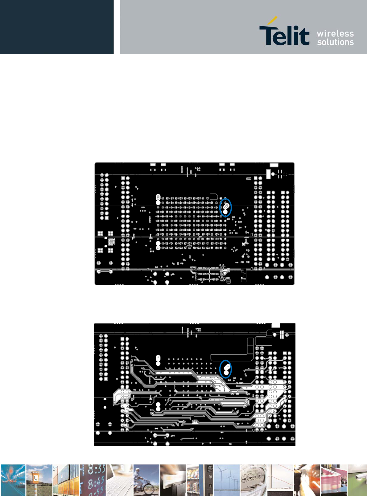
Here is the information of Telit’s approved interface
board layout and please see carefully the pictures
extracted from the gerber files for respective layer as
attached below.
This guidance should be referenced by OEM host.
Telit EVK for HE863 Family has a structure of six pcb
layers.
HE863 Family Hardware User Guide
1vv0300891 Rev.5- 2011-03-18
Reproduction forbidden without Telit Communications S.p.A’s. written authorization - All Rights
Reserved. Page 49 of 89
Layer1, Top layer:
The ball in blue circle is A3 which is assigned to the RF_ANT
in the HE863 Family. It is the starting point from the HE863
Family to an Antenna connector in a host system.
The trace info as; Thickness = 0.035 mm
Width = 1.0 mm
Length = 1.414 mm
Clearance = 0.775 mm (Signal to GND)
The actual trace limits in a host system should be calculated
to correspond to 50ohm and it may be provided by the pcb maker.
Layer2, inner layer:
It needs a cut-out on layer2 to meet 50ohm.
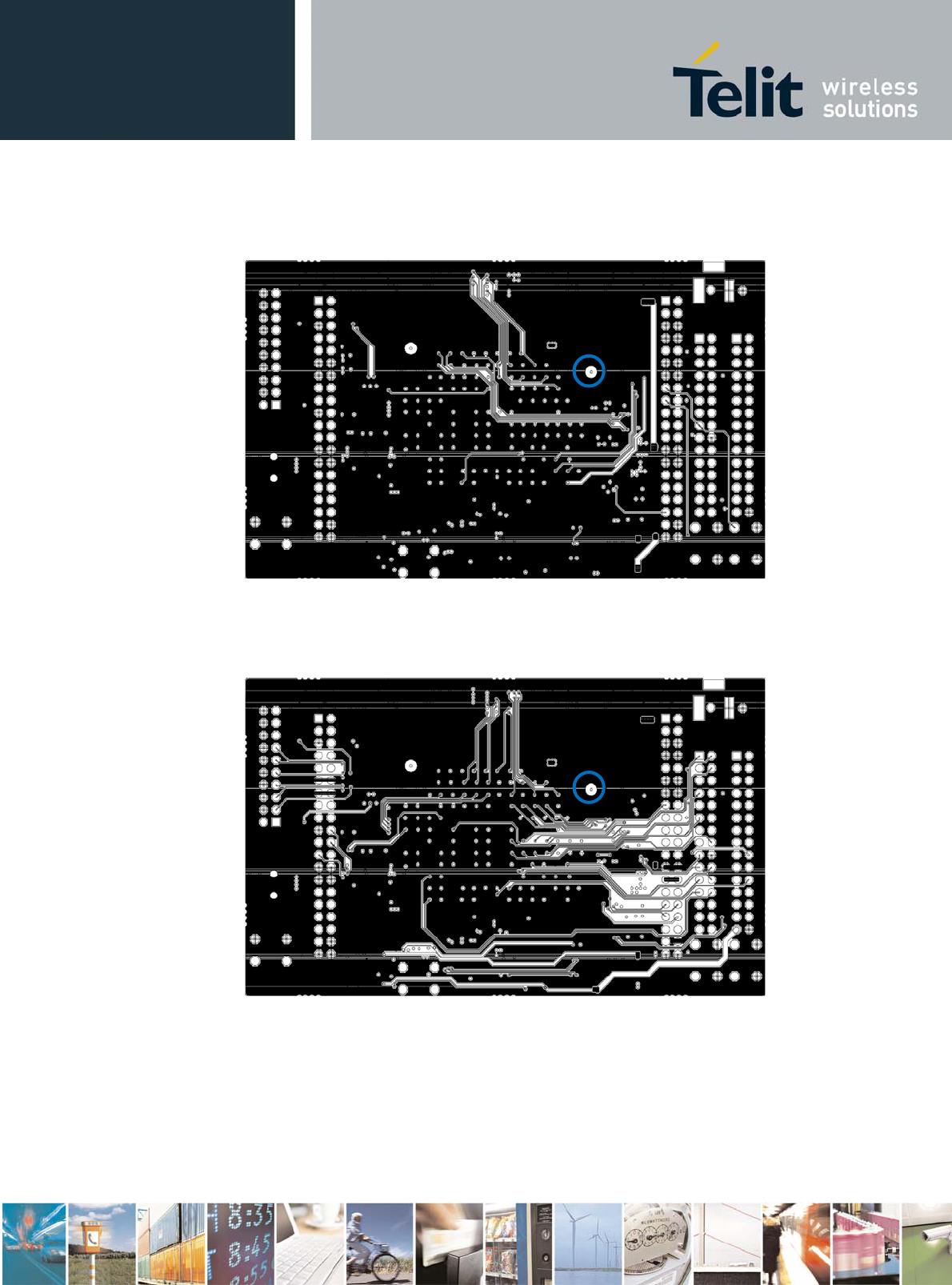
HE863 Family Hardware User Guide
1vv0300891 Rev.5- 2011-03-18
Reproduction forbidden without Telit Communications S.p.A’s. written authorization - All Rights
Reserved. Page 50 of 89
Layer3, inner layer:
There is no cut-out. The related via remains only.
Layer4, inner layer:
There is no cut-out. The related via remains only.
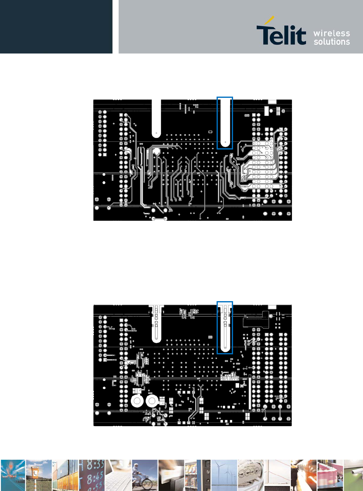
HE863 Family Hardware User Guide
1vv0300891 Rev.5- 2011-03-18
Reproduction forbidden without Telit Communications S.p.A’s. written authorization - All Rights
Reserved. Page 51 of 89
Layer5, inner layer:
Same cut-out with layer 6’s should be applied to match 50ohm.
Layer6, Bottom layer:
The trace info as; Thickness = 0.035 mm
Width = 1.2 mm
Length = 18.42 mm
Clearance = 2.0 mm (Signal to GND)
The actual trace limits in a host system should be calculated
to correspond to 50 ohm which may be provided by the pcb maker.
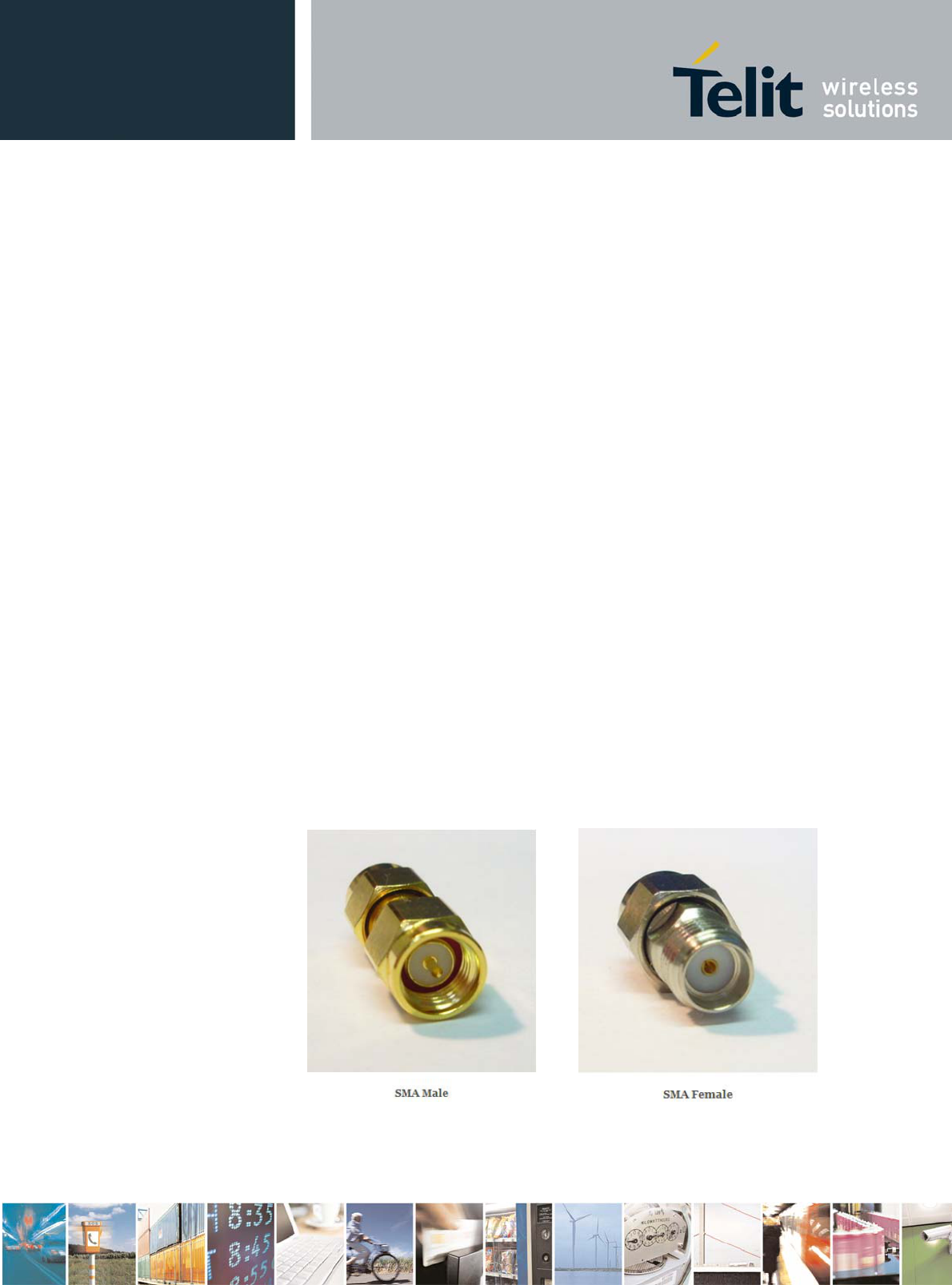
HE863 Family Hardware User Guide
1vv0300891 Rev.5- 2011-03-18
Reproduction forbidden without Telit Communications S.p.A’s. written authorization - All Rights
Reserved. Page 52 of 89
7.3. GSM/WCDMA Antenna – Installation Guidelines
Install the antenna in a place covered by the
GSM/WCDMA signal.
The Antenna must be installed to provide a separation
distance of at least 20 cm from all persons and must
not be co-located or operating in conjunction with any
other antenna or transmitter;
Antenna shall not be installed inside metal cases;
Antenna shall be installed also according Antenna
manufacturer instructions.
FCC Section 15.203 describes that the use of a
standard antenna jack or electrical connector is
prohibited.
Do NOT use this type of connector on the host system
and the host system should have one of special ones.
The host system designers should keep in mind this
information before they start their actual design.
Below descriptions will make it clearer.
According to the FCC requirement, SMA type is
prohibited because it is one of standard types but
the system designer can adopt RP-SMA type which is
considered a special type.
RP-SMA represents “Reversed Polarized SMA”.
Useful pictures below;
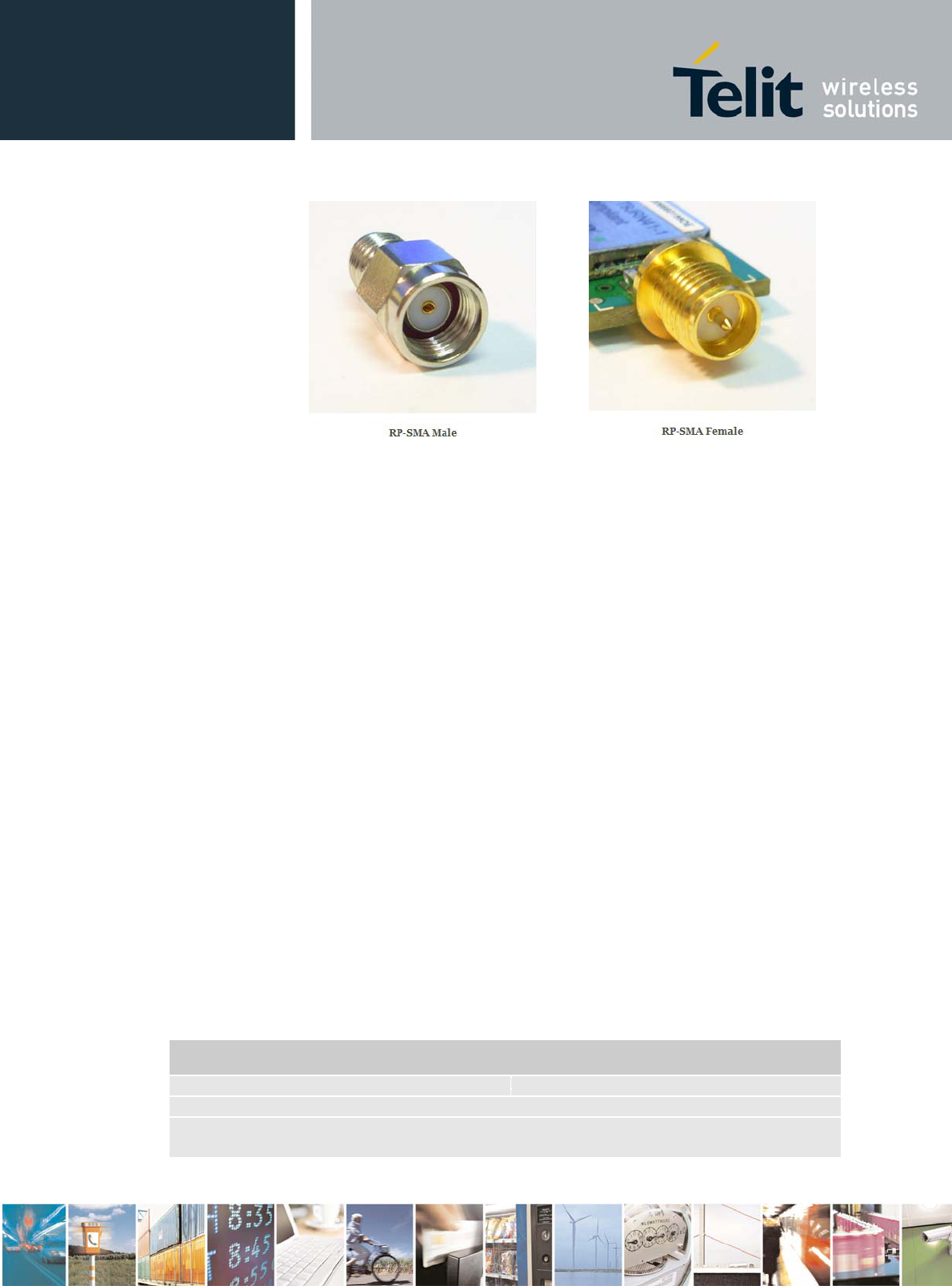
HE863 Family Hardware User Guide
1vv0300891 Rev.5- 2011-03-18
Reproduction forbidden without Telit Communications S.p.A’s. written authorization - All Rights
Reserved. Page 53 of 89
7.4. GPS Antenna Requirements (HE863-EUG/NAG/AUG
only)
The use of combined GPS antennas is NOT recommended; this
solution could generate an extremely poor GPS reception and
also the combination antenna requires additional diplexer and
adds a loss in the RF route.
The module is provided of an Antenna supply circuit with the
following characteristics:
Supply voltage referred to VBATT (Must accept values
from 3.4 to 4.2 V DC)
Supply enable controlled internally by the BB.
When using the Telit HE863-EUG/NAG/AUG, since there’s no
antenna connector on the module, the antenna must be connected
to the HE863-EUG/NAG/AUG through the PCB with the antenna pad
using a 50 Ohm transmission line.
In the case that the antenna is not directly developed on the
same PCB, hence directly connected at the antenna pad of the
HE863-EUG/NAG/AUG, then a PCB line is needed in order to
connect with it or with its connector.
This line of transmission shall fulfill the following
requirements:
ANTENNA LINE ON PCB REQUIREMENTS
Impedance 50 ohm
No coupling with other signals allowed
Cold End (Ground Plane) of antenna shall be equipotential to
the HE863-EUG/NAG/AUG ground pins.

HE863 Family Hardware User Guide
1vv0300891 Rev.5- 2011-03-18
Reproduction forbidden without Telit Communications S.p.A’s. written authorization - All Rights
Reserved. Page 54 of 89
Furthermore if the device is developed for the US and/or
Canada market, it must comply to the FCC and/or IC approval
requirements:
This device is to be used only for mobile and fixed
application.
7.5. GPS Antenna-PCB Line Guidelines (HE863-
EUG/NAG/AUG only)
Ensure that the antenna line impedance is 50 ohm;
Keep the antenna line on the PCB as short as possible
to reduce the loss.
Antenna line must have uniform characteristics,
constant cross section, avoid meanders and abrupt
curves;
Keep, if possible, one layer of the PCB used only for
the Ground plane;
Surround (on the sides, over and under) the antenna
line on PCB with Ground, avoid having other signal
tracks facing directly the antenna line track;
The ground around the antenna line on PCB has to be
strictly connected to the Ground Plane by placing vias
once per 2mm at least;
Place EM noisy devices as far as possible from HE863-
EUG/NAG/AUG antenna line;
Keep the antenna line far away from the HE863-
EUG/NAG/AUG power supply lines;
Keep the antenna line far away from the HE863-
EUG/NAG/AUG WCDMA/GSM RF lines;
If you have EM noisy devices around the PCB hosting
the HE863-EUG/NAG /AUG, such as fast switching ICs,
take care of the shielding of the antenna line by
burying it inside the layers of PCB and surround it
with Ground planes, or shield it with a metal frame
cover.
If you don't have EM noisy devices around the PCB of
HE863-EUG/NAG /AUG, by using a strip-line on the
superficial copper layer for the antenna line, the
line attenuation will be lower than a buried one;
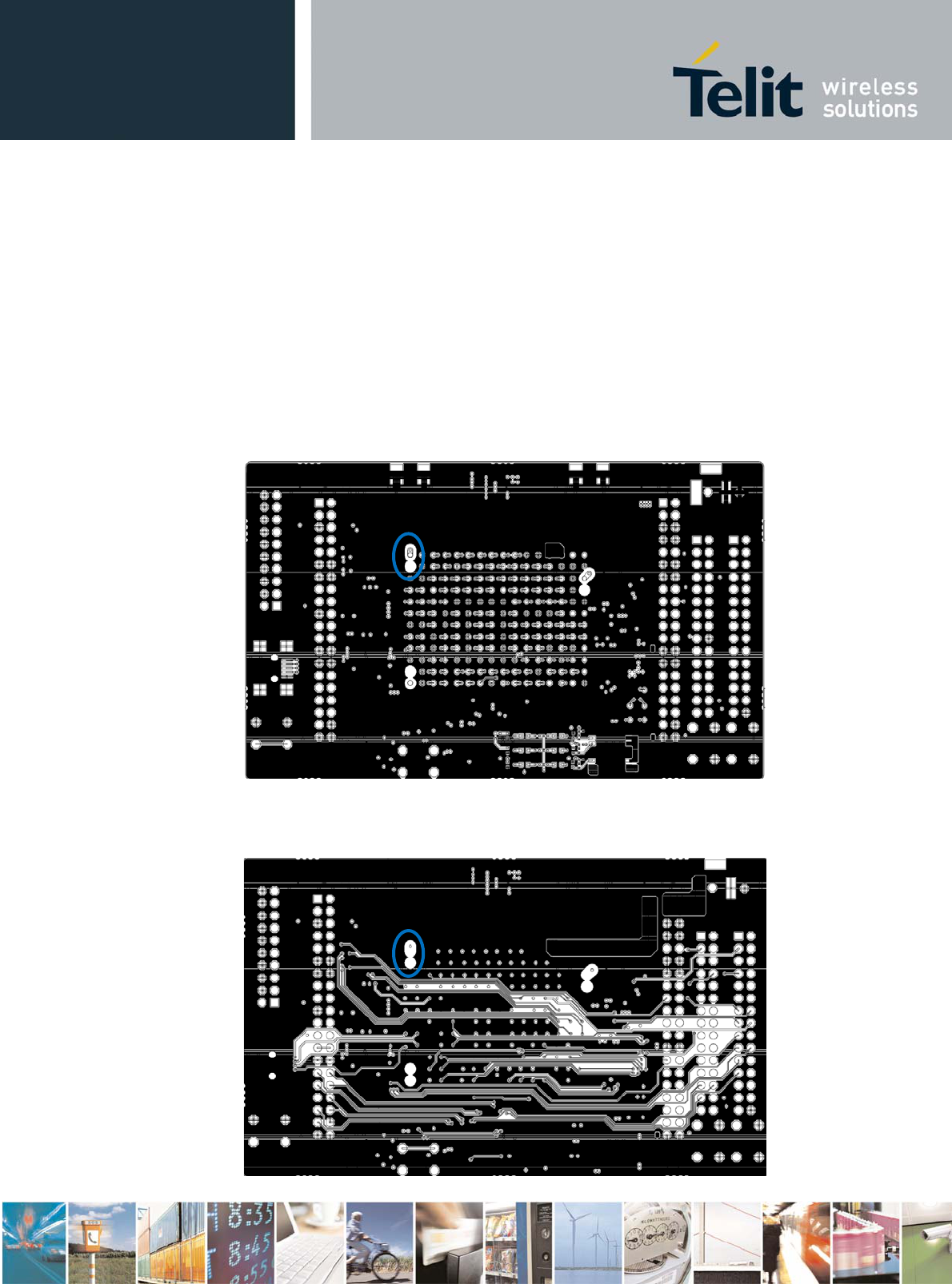
HE863 Family Hardware User Guide
1vv0300891 Rev.5- 2011-03-18
Reproduction forbidden without Telit Communications S.p.A’s. written authorization - All Rights
Reserved. Page 55 of 89
Here is the guidance for GPS antenna path.
Layer1, Top layer:
The ball in blue circle is S1 which is assigned to the GPS_ANT
in the HE863 Family. It is the starting point from the HE863
Family to an Antenna connector in a host system.
The trace info as; Thickness = 0.035 mm
Width = 1.0 mm
Length = 1.025 mm
Clearance = 0.775 mm (Signal to GND)
The actual trace limits in a host system should be calculated
to correspond to 50ohm and it may be provided by the pcb maker.
Layer2, inner layer:
It needs a cut-out on layer2 to meet 50ohm.
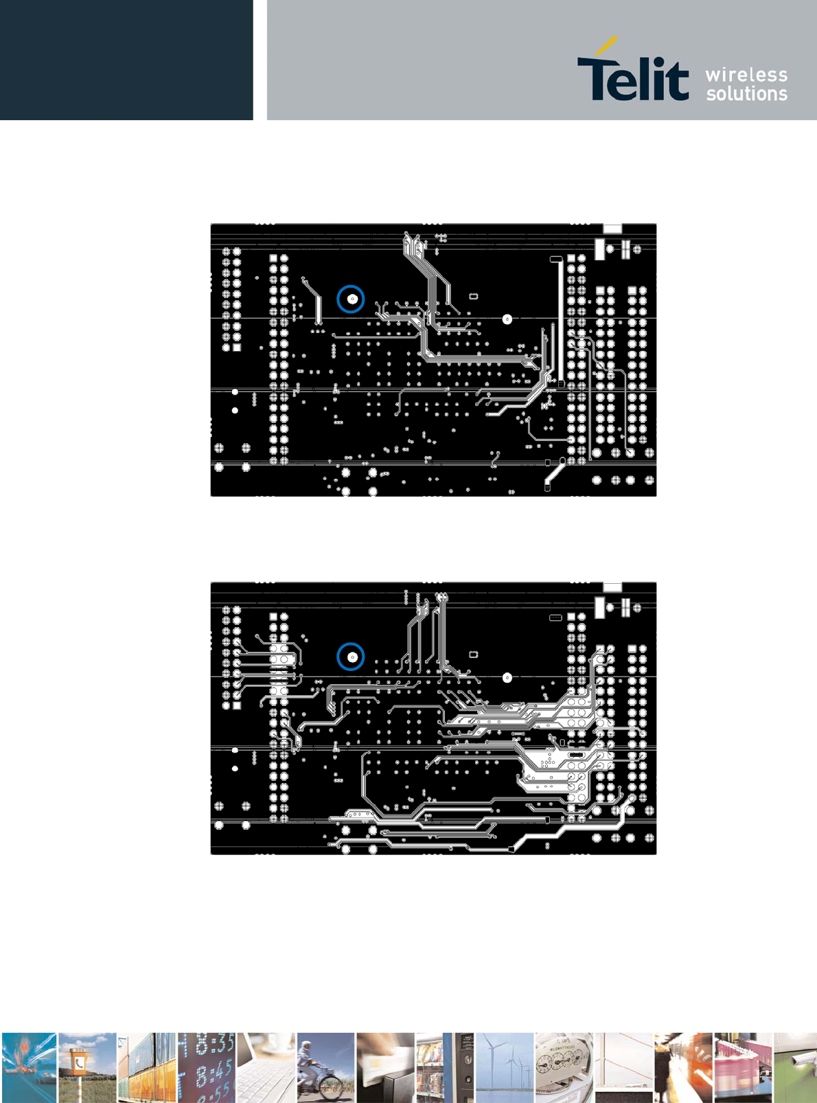
HE863 Family Hardware User Guide
1vv0300891 Rev.5- 2011-03-18
Reproduction forbidden without Telit Communications S.p.A’s. written authorization - All Rights
Reserved. Page 56 of 89
Layer3, inner layer:
There is no cut-out. The related via remains only.
Layer4, inner layer:
There is no cut-out. The related via remains only.
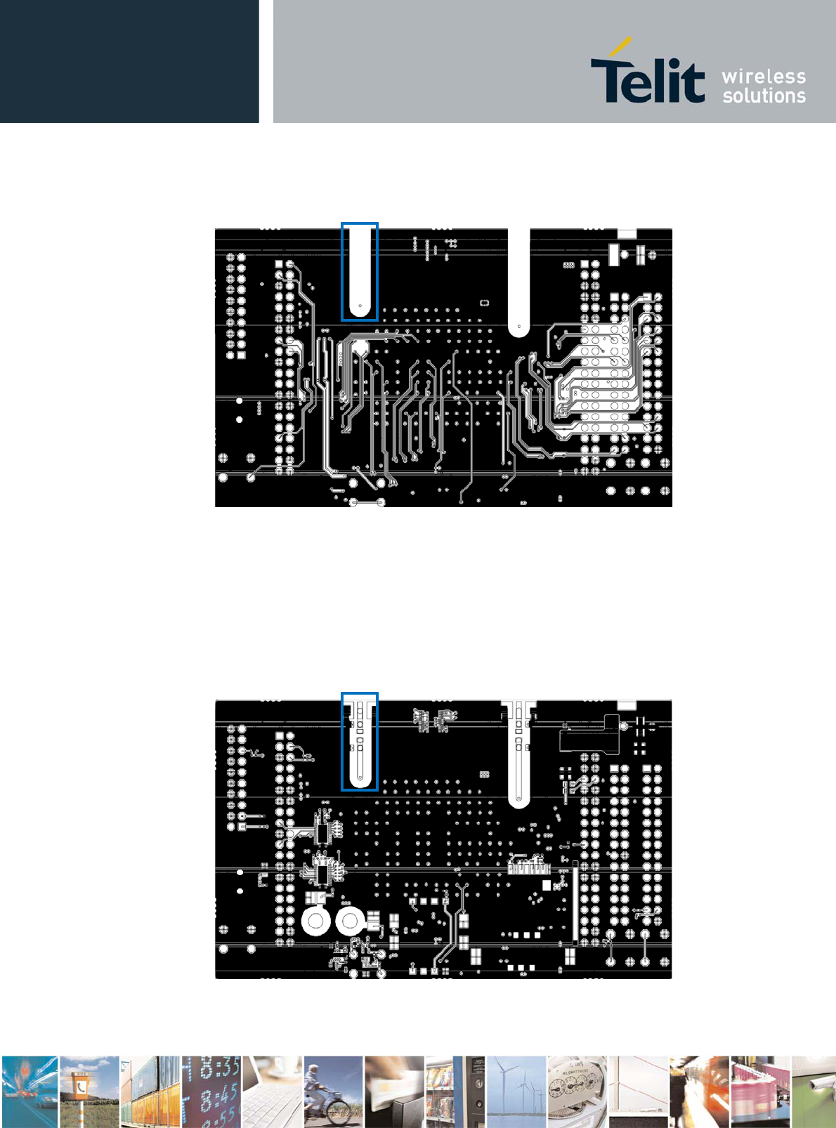
HE863 Family Hardware User Guide
1vv0300891 Rev.5- 2011-03-18
Reproduction forbidden without Telit Communications S.p.A’s. written authorization - All Rights
Reserved. Page 57 of 89
Layer5, inner layer:
Same cut-out with layer 6’s should be applied to match 50ohm.
Layer6, Bottom layer:
The trace info as; Thickness = 0.035 mm
Width = 1.2 mm
Length = 13.395 mm
Clearance = 2.0 mm (Signal to GND)
The actual trace limits in a host system should be calculated
to correspond to 50 ohm which may be provided by the pcb maker.

HE863 Family Hardware User Guide
1vv0300891 Rev.5- 2011-03-18
Reproduction forbidden without Telit Communications S.p.A’s. written authorization - All Rights
Reserved. Page 58 of 89
7.6. GPS Antenna-Installation Guidelines (HE863-
EUG/NAG/AUG only)
The HE863-EUG/NAG/AUG due to its characteristics of sensitivity is
capable to perform a Fix inside the buildings. (In any case the sensitivity
could be affected by the building characteristics i.e. shielding)
The Antenna must not be co-located or operating in conjunction with any
other antenna or transmitter;
Antenna shall not be installed inside metal cases
Antenna shall be installed also according Antenna manufacturer
instructions.
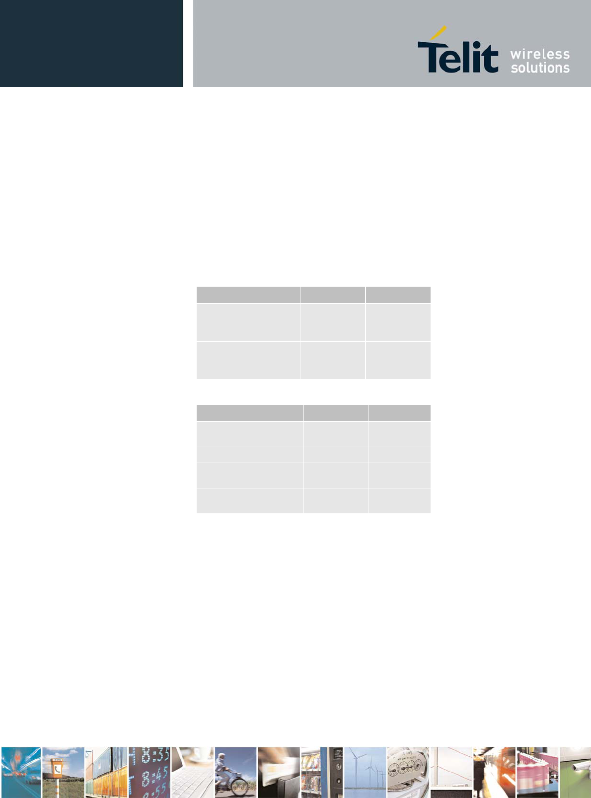
HE863 Family Hardware User Guide
1vv0300891 Rev.5- 2011-03-18
Reproduction forbidden without Telit Communications S.p.A’s. written authorization - All Rights
Reserved. Page 59 of 89
8. Logic Level Specifications
Where not specifically stated, all the interface circuits work
at 1.8V CMOS logic levels. The following table shows the logic
level specifications used in the Telit HE863 Family interface
circuits:
For 1.8V CMOS signals:
Absolute Maximum Ratings -Not Functional
Parameter Min Max
Input level on
any digital pin
when on
-0.3V +3.6V
Input voltage
on analog pins
when on
-0.15V +3.0 V
Operating Range - Interface levels
Level Min Max
Input high
level
1.26V 2.0 V
Input low level -0.2V 0.36V
Output high
level
1.6V 1.8V
Output low
level
0V 0.2V
HE863 Family Hardware User Guide
1vv0300891 Rev.5- 2011-03-18
Reproduction forbidden without Telit Communications S.p.A’s. written authorization - All Rights
Reserved. Page 60 of 89
8.1. Reset Signal
Signal Function I/O BGA Ball
RESET Phone
reset I G5
RESET is used to reset the HE863 Family module. Whenever this
signal is pulled low, HE863 Family is reset. When the device
is reset it stops all operations. After the release of the
reset HE863 Family is unconditionally shut down, without doing
any detach operations from the network where it is registered.
This behavior is not a proper shutdown because the device is
requested to issue a detach request on turn off. For this
reason, the Reset signal must not be used for normally
shutting down the device, but only as an emergency exit in the
rare case the device remains stuck waiting for some network
response.
The RESET is internally controlled on start-up to achieve
always a proper power-on reset sequence. There is no need to
control this pin on start-up. It may only be used to reset a
device already on that is not responding to any command.
NOTE:
Do not use this signal to power off HE863 Family.
Use AT#SHDN command to perform this function.
Reset Signal Operating levels:
Signal Min Max
RESET Input
high 2.0V* 2.6V
RESET Input low 0V 0.2V
* This signal is internally pulled up so the pin can be left
floating if not used.
If unused, this signal may be left unconnected. If used, it
must always be connected with an open collector transistor to
permit the internal circuitry the power on reset and under
voltage lockout functions.

HE863 Family Hardware User Guide
1vv0300891 Rev.5- 2011-03-18
Reproduction forbidden without Telit Communications S.p.A’s. written authorization - All Rights
Reserved. Page 61 of 89
9. Serial Ports
The serial port on the Telit HE863 Family is the interface
between the module and OEM hardware.
2 serial ports are available on the module:
MODEM SERIAL PORT;
MODEM SERIAL PORT 2 (DEBUG).
9.1. Modem Serial Port
Several configurations can be designed for the serial port on
the OEM hardware. The most common are:
RS232 PC com port;
microcontroller UART @ 1.8V – 2.0V (Universal
Asynchronous Receive Transmit) ;
Depending on the type of serial port on the OEM hardware, a
level translator circuit may be needed to make the system work.
The only configuration that does not need a level translation
is the 1.8V – 2.0V UART.
The serial port on HE863 Family is a +1.8V UART with all the 7
RS232 signals. It differs from the PC-RS232 in signal polarity
(RS232 is reversed) and levels. The levels for HE863 Family
UART are the CMOS levels:
Absolute Maximum Ratings -Not Functional
Parameter Min Max
Input level on any
digital pin when on -0.3V +3.6V
Input voltage on
analog pins when on -0.15V +3.0 V
Operating Range - Interface levels
Level Min Max
Input high level 1.26V 2.0 V
Input low level -0.2V 0.36V
Output high level 1.6V 1.8V
Output low level 0V 0.2V
HE863 Family Hardware User Guide
1vv0300891 Rev.5- 2011-03-18
Reproduction forbidden without Telit Communications S.p.A’s. written authorization - All Rights
Reserved. Page 62 of 89
The signals of the HE863 Family serial port are:
RS232
Pin
Number
Signal
HE863
Family
Ball
Name Usage
1
DCD -
dcd_uar
t
(TBD)
M3 Data Carrier
Detect
Output from the HE863 Family that
indicates the carrier presence
2 RXD -
Tx_uart J4 Transmit line
*see Note
Output transmit line of HE863 Family
UART
3 TXD -
Rx_uart J3 Receive line
*see Note Input receive of the HE863 Family UART
4
DTR -
dtr_uar
t
(TBD)
L3 Data Terminal
Ready
Input to the HE863 Family that controls
the DTE READY condition
5 GND All GND Ground ground
6
DSR -
dsr_uar
t
(TBD)
L4 Data Set
Ready
Output from the HE863 Family that
indicates the module is ready
7
RTS -
rts_uar
t
K3 Request to
Send
Input to the HE863 Family that controls
the Hardware flow control
8
CTS -
cts_uar
t
K4 Clear to Send Output from the HE863 Family that
controls the Hardware flow control
9
RI -
ri_uart
(TBD)
M4 Ring
Indicator
Output from the HE863 Family that
indicates the Incoming call condition
TIP:
For minimum implementation, only the TXD and RXD lines can be
connected, the other lines can be left open provided a
software flow control is implemented.
NOTE:
According to V.24, RX/TX signal names are referred to the
application side, therefore on the HE863 Family side these
signal are on the opposite direction: TXD on the application
side will be connected to the receive line (here named TXD/
rx_uart ) of the HE863 Family serial port and vice versa for
RX.
HE863 Family Hardware User Guide
1vv0300891 Rev.5- 2011-03-18
Reproduction forbidden without Telit Communications S.p.A’s. written authorization - All Rights
Reserved. Page 63 of 89
9.2. RS232 Level Translation
In order to interface the Telit HE863 Family with a PC com
port or a RS232 (EIA/TIA-232) application a level translator
is required. This level translator must:
invert the electrical signal in both directions;
Change the level from 0/1.8V to +15/-15V.
Actually, the RS232 UART 16450, 16550, 16650 & 16750 chipsets
accept signals with lower levels on the RS232 side (EIA/TIA-
562), allowing a lower voltage-multiplying ratio on the level
translator. Note that the negative signal voltage must be less
than 0V and hence some sort of level translation is always
required.
The simplest way to translate the levels and invert the signal
is by using a single chip level translator. There are a
multitude of them, differing in the number of drivers and
receivers and in the levels (be sure to get a true RS232 level
translator not a RS485 or other standards).
By convention the driver is the level translator from the 0-
1.8V UART to the RS232 level. The receiver is the translator
from the RS232 level to 0-1.8V UART.
In order to translate the whole set of control lines of the
UART you will need:
5 drivers
3 receivers
NOTE:
The digital input lines working at 1.8V CMOS have an absolute
maximum input voltage of 3.6V; therefore the level translator
IC shall not be powered by the +3.8V supply of the module.
Instead, it must be powered from a +1.8V / +2.0V (dedicated)
power supply.
This is because in this way the level translator IC outputs on
the module side (i.e. HE863 Family inputs) will work at +3.8V
interface levels, damaging the module inputs.
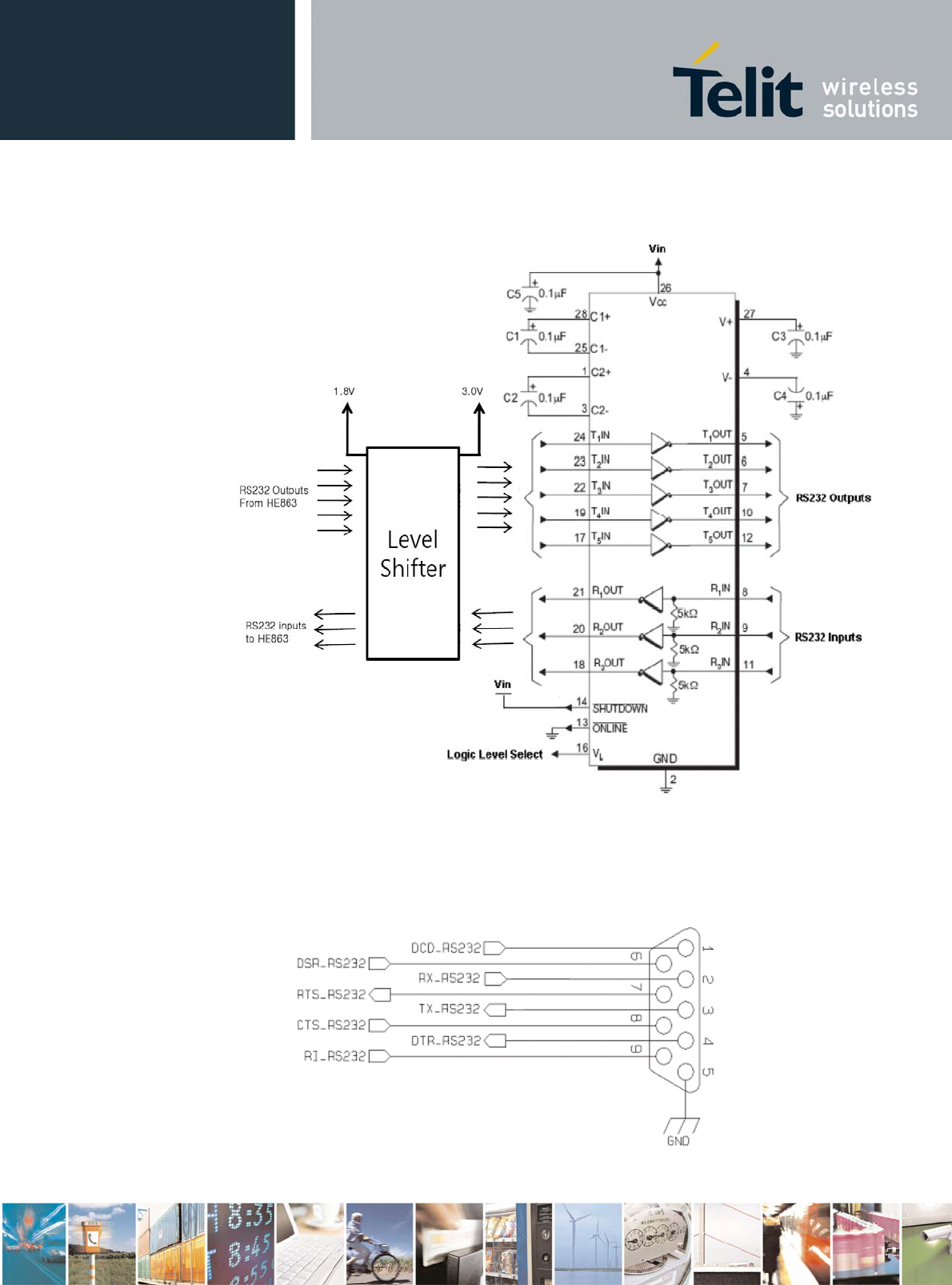
HE863 Family Hardware User Guide
1vv0300891 Rev.5- 2011-03-18
Reproduction forbidden without Telit Communications S.p.A’s. written authorization - All Rights
Reserved. Page 64 of 89
An example of level translation circuitry of this kind is:
The RS232 serial port lines are usually connected to a DB9
connector with the following layout: signal names and
directions are named and defined from the DTE point of view.
HE863 Family Hardware User Guide
1vv0300891 Rev.5- 2011-03-18
Reproduction forbidden without Telit Communications S.p.A’s. written authorization - All Rights
Reserved. Page 65 of 89
10. USB Port
The HE863 Family module includes a Universal Serial Bus (USB)
transceiver, which operates at USB low-speed (1.5Mbits/sec),
USB full-speed (12Mbits/sec) and USB high-speed (480Mbits/sec).
It is compliant with the USB 2.0 specification and can be used
for diagnostic monitoring, control and data transfers.
The table below describes the USB interface signals:
TIP:
The HE863 Family does NOT support host device operation at the
moment, that is, it works as a slave device.
10.1. USB transceiver specifications (TBD)
Signal
HE863
Family
Ball Usage
USB_VBUS S8
Power supply for the internal USB transceiver.
This pin is configured as an analog input or an
analog output depending upon the type of
peripheral device connected.
USB_D- R8
Minus (-) line of the differential, bi-
directional USB signal to/from the peripheral
device
USB D+ R9
Plus (+) line of the differential, bi-
directional USB signal to/from the peripheral
device
USB_ID
(TBD) S9
Analog input used to sense whether a peripheral
device is
connected and if connected, to determine the
peripheral type, host or slave

HE863 Family Hardware User Guide
1vv0300891 Rev.5- 2011-03-18
Reproduction forbidden without Telit Communications S.p.A’s. written authorization - All Rights
Reserved. Page 66 of 89
11. Audio Section (HE863-EUR/EUG/NAR/NAG/AUG only)
The Baseband chip was developed for the cellular phones, which
needed two separated amplifiers both in RX and in TX section.
A couple of amplifiers had to be used with internal audio
transducers while the other couple of amplifiers had to be
used with external audio transducers.
To distinguish the schematic signals and the Software
identifiers, two different definitions were introduced, with
the following meaning:
internal audio transducers HS/MT differential/Single
ended type (from HandSet or MicroTelephone )
external audio transducers HF only single-ended output
type (from HandsFree )
Actually the acronyms have not the original importance.
In other words this distinction is not necessary, being the
performances between the two blocks like the same.
Only if the customer needs higher output power to the speaker,
he has a constraint. Otherwise the choice could be done in
order to overcome the PCB design difficulties.
For these reasons we have not changed the HS and HF acronyms,
keeping them in the Software and on the schematics.
11.1. Selection mode
Only one block can be active at a time, and the activation of
the requested audio path is done via hardware by AXE line or
via software by AT#CAP command.
Moreover the Sidetone functionality could be implemented by
the amplifier fitted between the transmit path and the receive
path, enabled at request in both modes.
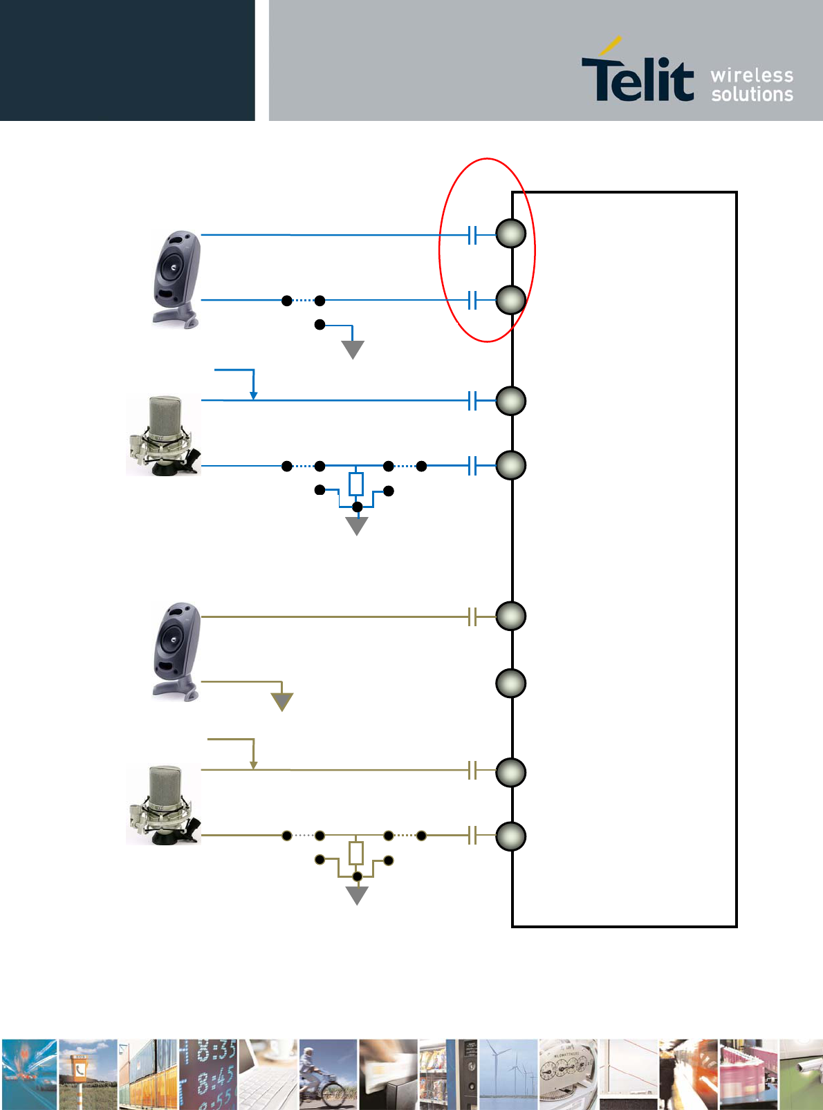
HE863 Family Hardware User Guide
1vv0300891 Rev.5- 2011-03-18
Reproduction forbidden without Telit Communications S.p.A’s. written authorization - All Rights
Reserved. Page 67 of 89
100nF
100nF
100nF
100nF
100nF
Bias
Single ended
Differential or Single ended
Only Single ended
Baseband AFE
EAR_MT+ (EPP1)
EAR_MT- (EPN1)
MIC_MT- (MICN1)
Single ended
Differential
MIC_MT+ (MICP1)
Differential or Single ended
100nF
100nF
Bias
Differential
Single ended
Differential or Single ended
MIC_HF- (AUX2N)
MIC_HF+ (AUX1N)
EAR_HF+ (EPPA2)
EAR_HF- (EPPA1)
Reserved Ball
Differential
16Ω
16Ω

HE863 Family Hardware User Guide
1vv0300891 Rev.5- 2011-03-18
Reproduction forbidden without Telit Communications S.p.A’s. written authorization - All Rights
Reserved. Page 68 of 89
11.2. Microphone Characteristics
TIP:
Being the microphone circuitry the more noise sensitive, its
design and layout must be realized with particular care. Both
microphone paths are balanced and the OEM circuitry must be
balanced designed to reduce the common mode noise typically
generated on the ground plane. However the customer can use
the unbalanced circuitry for particular application.
11.2.1. Input Lines (MIC1 and MIC2) Characteristics (TBD)
Line coupling
Line type
Coupling capacitor
Differential input
impedance
Differential input
voltage
11.3. OUTPUT LINES (Speaker)
We suggest driving the load differentially from both output
drivers, thus the output swing will double and the need for the
output coupling capacitor avoided.
If a particular OEM application needs a Single Ended Output
configuration the output power will be reduced four times.
The OEM circuitry shall be designed to reduce the common mode
noise typically generated on the ground plane and to get the
maximum power output from the device (low resistance tracks).
(*) WARNING:
Using single ended configuration, the unused output line must
be left open.
Not respecting this constraint, the output stage will be
damaged.
HE863 Family Hardware User Guide
1vv0300891 Rev.5- 2011-03-18
Reproduction forbidden without Telit Communications S.p.A’s. written authorization - All Rights
Reserved. Page 69 of 89
DANGER:
Using HS/MT, the serial capacitors below 100nF must be
connected in the output lines.
The handsfree mode only supports single ended type and
reserved HF- Ball must be opened.
11.3.1. Output Lines Characteristics (TBD)
Line coupling
differential
single-ended
DC
AC
Output load impedance
differential
16 Ω
Differential output impedance
Signal bandwidth 150 - 4000 Hz @ -3 dB
Differential output voltage
(typ.)
1060 mVrms /16 Ω
Max Output Power
@ 16 Ω
Max load capacitance
Table 3. “Ear_MT” Output (EAR_EPP1 differential amplifier)
Line coupling
differential
single-ended
Output load impedance
single-ended
16 Ω (≤ 26)
S.E. output impedance ≤ 0,5 Ω @ 1.02kHz
signal bandwidth 150 - 4000 Hz @ -3 dB
Differential output voltage
(typ.)
833 mVrms /16 Ω
Max Output Power
@ 16Ω
Max load capacitance
Table 4. “Ear_HF” Output (EAR_EPPA2 amplifiers)
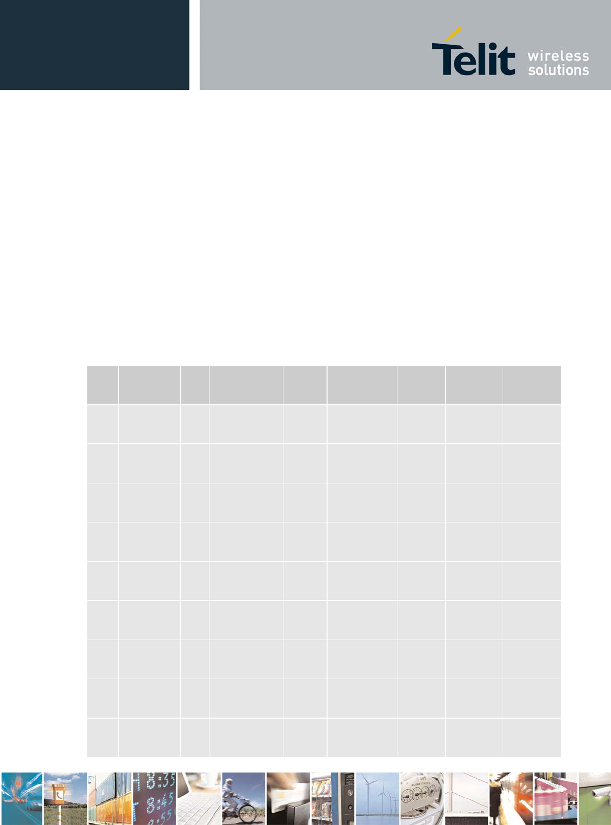
HE863 Family Hardware User Guide
1vv0300891 Rev.5- 2011-03-18
Reproduction forbidden without Telit Communications S.p.A’s. written authorization - All Rights
Reserved. Page 70 of 89
12. General Purpose I/O
The general-purpose I/O pads can be configured to act in three
different ways:
input
output
alternate function (internally controlled)
Input pads can only be read and report the digital value (high
or low) present on the pad at the read time; output pads can
only be written or queried and set the value of the pad
output; an alternate function pad is internally controlled by
the HE863 Family firmware and acts depending on the function
implemented.
The following GPIOs are available on the HE863 Family.
Bal
l Signal I/O Function Type Drive
strength
Defaul
t
State
ON_OFF
State Note
J11 TGPIO_01 I/O
GPIO01
Configura
ble GPIO
CMOS
1.8V 2mA INPUT LOW
G9 TGPIO_02 I/O
GPIO02
Configura
ble GPIO
CMOS
1.8V 2mA INPUT LOW
K11 TGPIO_03 I/O
GPIO03
Configura
ble GPIO
CMOS
1.8V 2mA INPUT LOW
F9 TGPIO_04 I/O
GPIO04
Configura
ble GPIO
CMOS
1.8V 2mA INPUT LOW
F10 TGPIO_05 I/O
GPIO05
Configura
ble GPIO
CMOS
1.8V 2mA INPUT LOW
E10 TGPIO_06 I/O
GPIO06
Configura
ble GPIO
CMOS
1.8V 2mA INPUT LOW
Alternate
function
(ALARM)
E9 TGPIO_07 I/O
GPIO07
Configura
ble GPIO
CMOS
1.8V 2mA INPUT LOW
B10 TGPIO_08 I/O
GPIO08
Configura
ble GPIO
CMOS
1.8V 2mA INPUT LOW
N12 TGPIO_09 I/O
GPIO09
Configura
ble GPIO
CMOS
1.8V 2mA INPUT LOW
HE863 Family Hardware User Guide
1vv0300891 Rev.5- 2011-03-18
Reproduction forbidden without Telit Communications S.p.A’s. written authorization - All Rights
Reserved. Page 71 of 89
M8 TGPIO_10 I/O
GPIO10
Configura
ble GPIO
CMOS
1.8V 2mA INPUT LOW
Alternate
function
(PCM_TX)
-R/-G only
P12 TGPIO_11 I/O
GPIO11
Configura
ble GPIO
CMOS
1.8V 2mA INPUT LOW
L12 TGPIO_12 I/O
GPIO12
Configura
ble GPIO
CMOS
1.8V 2mA INPUT LOW
N11 TGPIO_13 I/O
GPIO13
Configura
ble GPIO
CMOS
1.8V 2mA INPUT LOW
P11 TGPIO_14 I/O
GPIO14
Configura
ble GPIO
CMOS
1.8V 2mA INPUT LOW
M12 TGPIO_15 I/O
GPIO15
Configura
ble GPIO
CMOS
1.8V 2mA INPUT LOW
N10 TGPIO_16 I/O
GPIO16
Configura
ble GPIO
CMOS
1.8V 2mA INPUT LOW
M7 TGPIO_17 I/O
GPIO17
Configura
ble GPIO
CMOS
1.8V 2mA INPUT LOW
Alternate
function
(PCM_SYNC)
-R/-G only
M9 TGPIO_18 I/O
GPIO18
Configura
ble GPIO
CMOS
1.8V 2mA INPUT LOW
Alternate
function
(PCM_RX)
-R/-G only
P10 TGPIO_19 I/O
GPIO19
Configura
ble GPIO
CMOS
1.8V 2mA INPUT LOW
M11 TGPIO_20 I/O
GPIO20
Configura
ble GPIO
CMOS
1.8V 2mA INPUT LOW
K12 TGPIO_21 I/O
GPIO21
Configura
ble GPIO
CMOS
1.8V 2mA INPUT HIGH
L11 TGPIO_22 I/O
GPIO22
Configura
ble GPIO
CMOS
1.8V 2mA INPUT LOW
Not all GPIO pads support all these three modes:
GPIO6 supports all three modes and can be input,
output, alarm output (Alternate function)
Some alternate functions for HE863 Family may be added if
needed.

HE863 Family Hardware User Guide
1vv0300891 Rev.5- 2011-03-18
Reproduction forbidden without Telit Communications S.p.A’s. written authorization - All Rights
Reserved. Page 72 of 89
12.1. Logic Level Specifications
Where not specifically stated, all the interface circuits work
at 1.8V CMOS logic levels.
The following table shows the logic level specifications used
in the HE863 Family interface circuits:
For 1.8V CMOS signals:
Absolute Maximum Ratings -Not Functional
Parameter Min Max
Input level on
any digital pin
when on
-0.3V +3.6V
Input voltage
on analog pins
when on
-0.15V +3.0 V
Operating Range - Interface levels
Level Min Max
Input high
level
1.26V 2.0 V
Input low level -0.2V 0.36V
Output high
level
1.6V 1.8V
Output low
level
0V 0.2V
12.2. Using a GPIO Pad as Input
The GPIO pads, when used as inputs, can be connected to a
digital output of another device and report its status,
provided this device has interface levels compatible with the
1.8V CMOS levels of the GPIO.
If the digital output of the device is connected with the GPIO
input, the pad has interface levels different from the 1.8V
CMOS. It can be buffered with an open collector transistor
with a 47KΩ pull-up resistor to 1.8V.
12.3. Using a GPIO Pad as Output
The GPIO pads, when used as outputs, can drive 1.8V CMOS
digital devices or compatible hardware. When set as outputs,
HE863 Family Hardware User Guide
1vv0300891 Rev.5- 2011-03-18
Reproduction forbidden without Telit Communications S.p.A’s. written authorization - All Rights
Reserved. Page 73 of 89
the pads have a push-pull output and therefore the pull-up
resistor may be omitted.
12.4. Using the Alarm Output GPIO6
The GPIO6 pad, when configured as Alarm Output, is controlled
by the HE863 Family module and will rise when the alarm starts
and fall after the issue of a dedicated AT command.
This output can be used to power up the HE863 Family
controlling microcontroller or application at the alarm time,
giving you the possibility to program a timely system wake-up
to achieve some periodic actions and completely turn off
either the application or the HE863 Family during sleep
periods. This will dramatically reduce the sleep consumption
to few μA.
In battery-powered devices this feature will greatly improve
the autonomy of the device.
NOTE:
During RESET the line is set to HIGH logic level.
12.5. Indication of Network Service Availability
The STAT_LED pin status shows information on the network
service availability and Call status. In the HE863 Family
modules, the STAT_LED usually needs an external transistor to
drive an external LED. Because of the above, the status
indicated in the following table is reversed with respect to
the pin status:
LED status Device Status
Permanently off Device off
Fast blinking
(Period 1s, Ton 0,5s)
Net search /
Not registered /
turning off
Slow blinking
(Period 3s, Ton 0,3s) Registered full service
Permanently on a call is active
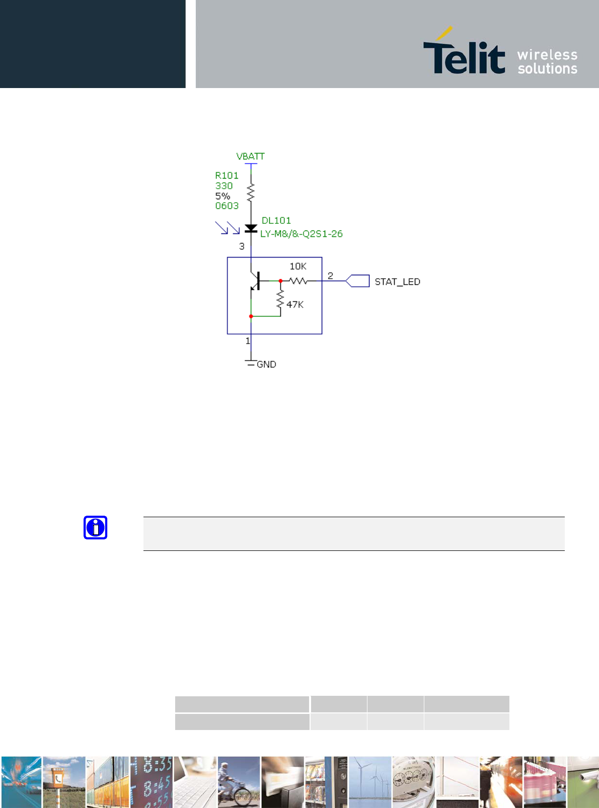
HE863 Family Hardware User Guide
1vv0300891 Rev.5- 2011-03-18
Reproduction forbidden without Telit Communications S.p.A’s. written authorization - All Rights
Reserved. Page 74 of 89
12.6. RTC Bypass Out
The VRTC pin brings out the Real Time Clock supply, which is
separate from the rest of the digital part, allowing having
only RTC going on when all the other parts of the device are
off. To this power output a backup capacitor can be added in
order to increase the RTC autonomy during power off of the
battery.
NOTE:
NO devices must be powered from this pin.
12.7. VAUX1 Power Output
A regulated power supply output is provided in order to supply
small devices from the module. This output is active when the
module is ON and goes OFF when the module is shut down. The
operating range characteristics of the supply are:
Operating Range – VAUX1 power supply
Min Typical Max
Output voltage 1.75V 1.8V 1.85V

HE863 Family Hardware User Guide
1vv0300891 Rev.5- 2011-03-18
Reproduction forbidden without Telit Communications S.p.A’s. written authorization - All Rights
Reserved. Page 75 of 89
Output current 100mA
Output bypass
capacitor
(Inside the module)
1μF

HE863 Family Hardware User Guide
1vv0300891 Rev.5- 2011-03-18
Reproduction forbidden without Telit Communications S.p.A’s. written authorization - All Rights
Reserved. Page 76 of 89
13. DAC and ADC section
13.1. DAC Converter
13.1.1. Description
The HE863 Family module provides a Digital to Analog Converter.
The signal (named DAC_OUT) is available on BGA Ball S4 of the
HE863 Family module.
The on board DAC is a 16-bit converter, able to generate an
analogue value based on a specific input in the range from 0
up to 65535 but recalibrated in the range from 0 to 1023.
However, an external low-pass filter is necessary.
Min Max Units
Voltage range
(filtered)
0 1.8 Volt
Range 0 1023 Steps
The precision is 1023 steps, so if we consider that the
maximum voltage is 1.8V, the integrated voltage could be
calculated with the following formula:
Integrated output voltage = 1.8 * value / 1023
DAC_OUT line must be integrated (for example with a low band
pass filter) in order to obtain an analog voltage.
13.1.2. Enabling DAC
An AT command is available to use the DAC function. The
command is:AT#DAC[=<enable>[,<value>]]
<value> - scale factor of the integrated output voltage
(0..1023 - 10 bit precision)
it must be present if <enable>=1
Refer to SW User Guide or AT Commands Reference Guide for the
full description of this function.
NOTE:
The DAC frequency is selected internally. D/A converter must
not be used during POWERSAVING.
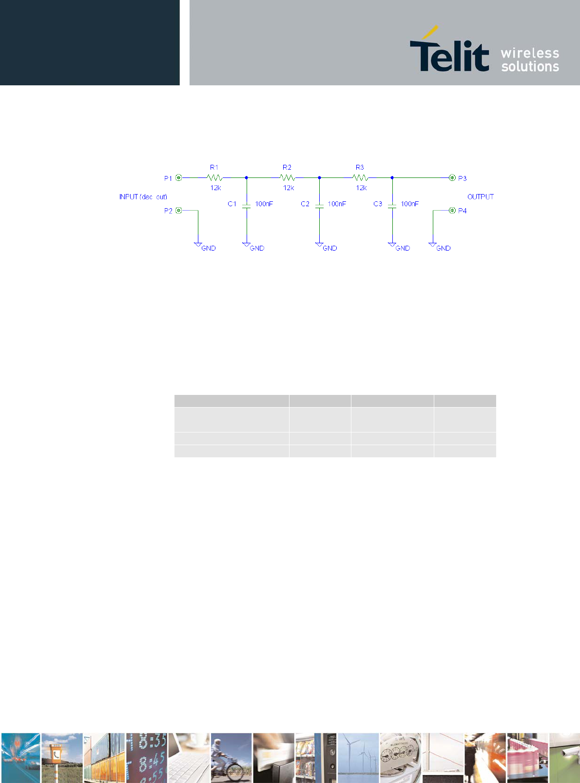
HE863 Family Hardware User Guide
1vv0300891 Rev.5- 2011-03-18
Reproduction forbidden without Telit Communications S.p.A’s. written authorization - All Rights
Reserved. Page 77 of 89
13.1.3. Low Pass Filter Example
13.2. ADC Converter
13.2.1. Description
The on board ADCs are 10-bit converters. They are able to read
a voltage level in the range of 0-1.2 volts applied on the ADC
pin input and store and convert it into 10 bit word.
Min Max Units
Input Voltage
range
0 1.2 Volt
AD conversion - 10 bits
Resolution - < 1.2 mV
The HE863 Family module provides 3 Analog to Digital
Converters. The input lines are:
ADC_IN1 is available on BGA Ball R4 of the HE863 Family module.
ADC_IN2 is available on BGA Ball R5 of the HE863 Family module.
ADC_IN3 is available on BGA Ball S5 of the HE863 Family module.
13.2.2. Using ADC Converter
An AT command is available to use the ADC function.
The command is AT#ADC=1,2 The read value is expressed in mV
Refer to SW User Guide or AT Commands Reference Guide for the
full description of this function.
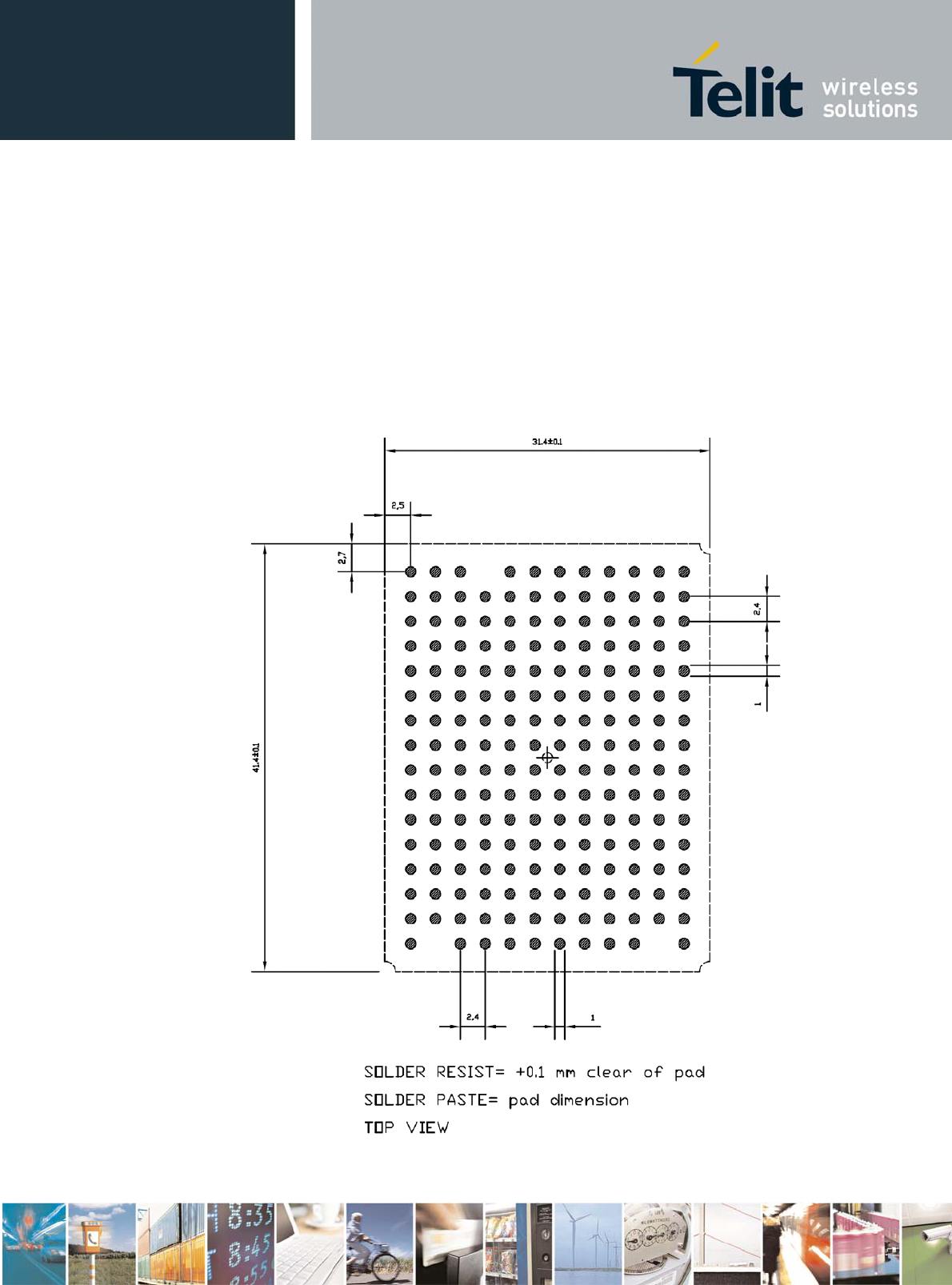
HE863 Family Hardware User Guide
1vv0300891 Rev.5- 2011-03-18
Reproduction forbidden without Telit Communications S.p.A’s. written authorization - All Rights
Reserved. Page 78 of 89
14. Mounting the HE863 Family on your board
14.1. General
The Telit HE863 Family module has been designed in order to be
compliant with a standard lead-free SMT process.
14.1.1. Recommended footprint for the application
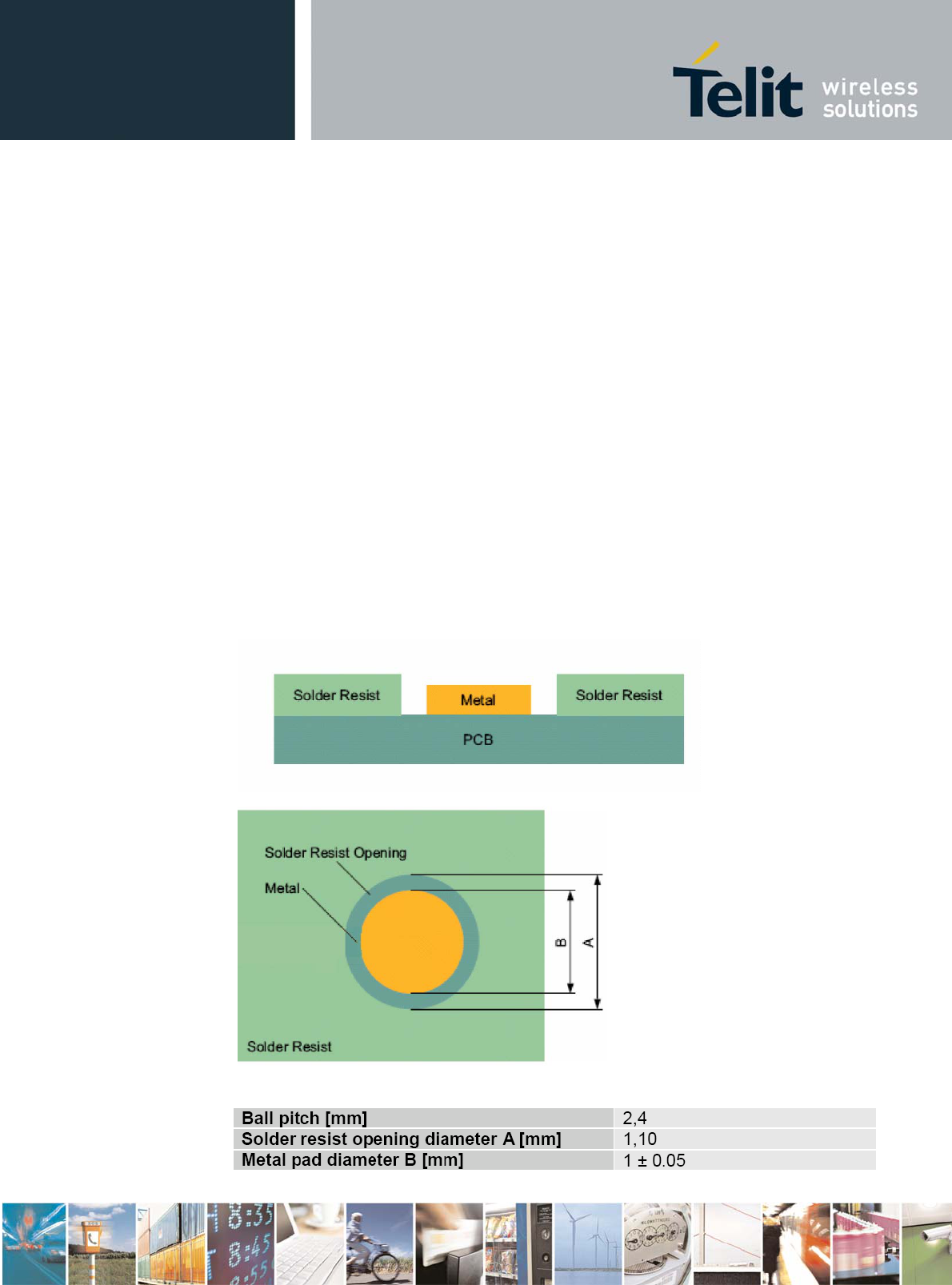
HE863 Family Hardware User Guide
1vv0300891 Rev.5- 2011-03-18
Reproduction forbidden without Telit Communications S.p.A’s. written authorization - All Rights
Reserved. Page 79 of 89
14.1.2. Suggested Inhibit Area
In order to easily rework the HE863 Family it is suggested to
consider on the application a 1.5mm Inhibit area around the
module.
It is also suggested, as common rule for an SMT component, to
avoid having a mechanical part of the application in direct
contact with the module.
14.1.3. Stencil
Stencil’s apertures layout can be the same of the recommended
footprint (1:1), we suggest a thickness of stencil foil ≥
120µm.
14.1.4. PCB Pad Design
“Non solder mask defined” (NSMD) type is recommended for the
solder pads on the PCB.
Recommendations for PCB pad dimensions
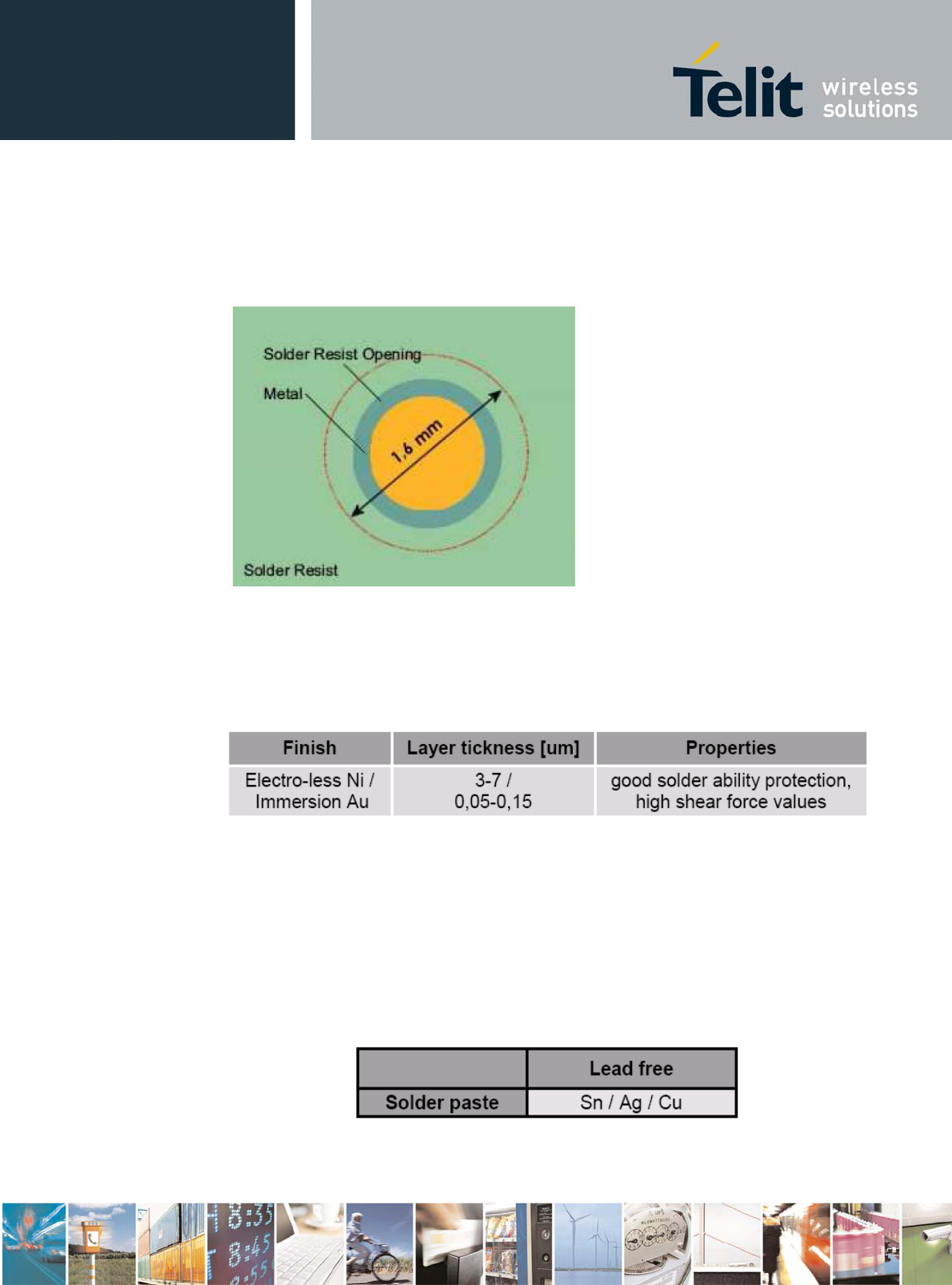
HE863 Family Hardware User Guide
1vv0300891 Rev.5- 2011-03-18
Reproduction forbidden without Telit Communications S.p.A’s. written authorization - All Rights
Reserved. Page 80 of 89
Placement of microvias not covered by solder resist is not
recommended, unless the microvia carries the same signal of the
pad itself.
Holes in pad are allowed only for blind holes and not for
through holes.
Recommendations for PCB pad surfaces:
The PCB must be able to resist the higher temperatures, which
are occurring at the lead-free process. This issue should be
discussed with the PCB-supplier. Generally, the wet-ability of
tin-lead solder paste on the described surface plating is
better compared to lead-free solder paste.
14.1.5. Solder paste
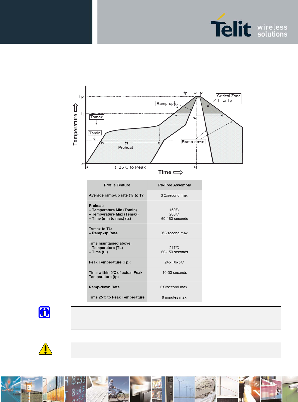
HE863 Family Hardware User Guide
1vv0300891 Rev.5- 2011-03-18
Reproduction forbidden without Telit Communications S.p.A’s. written authorization - All Rights
Reserved. Page 81 of 89
14.1.6. HE863 Family Solder Reflow
The following is the recommended solder reflow profile
NOTE:
All temperatures refer to topside of the package, measured on
the package body surface.
WARNING:
HE863 Family module can accept only one reflow process.

HE863 Family Hardware User Guide
1vv0300891 Rev.5- 2011-03-18
Reproduction forbidden without Telit Communications S.p.A’s. written authorization - All Rights
Reserved. Page 82 of 89
14.2. DEBUG OF THE HE863 Family IN PRODUCTION
To test and debug the mounting of HE863 Family, we strongly
recommend foreseeing test pads on the host PCB, in order to
check the connection between the HE863 Family itself and the
application and to test the performance of the module
connecting it with an external computer. Depending on the
customer application, these pads include, but are not limited
to the following signals:
TXD
RXD
ON/OFF
RESET
GND
VBATT
TX_TRACE
RX_TRACE
PWRMON

HE863 Family Hardware User Guide
1vv0300891 Rev.5- 2011-03-18
Reproduction forbidden without Telit Communications S.p.A’s. written authorization - All Rights
Reserved. Page 83 of 89
15. SIM holder design guide
15.1. Overview
In HE863 Family modules there are five pins for SIM card holder
connection.
These lines are:
SIMVCC (SIM Power supply)
SIMRST (SIM Reset)
SIMIO (SIM Data)
SIMIN (SIM Presence/Absence) (TBD)
SIMCLK (SIM Clock)
SIM connection must take in account of three key issues:
1) Data Integrity: standard rules for digital layout and
routing must be followed taking in consideration that SIMCLK
has frequency of 3.57 MHz and SIMIO has 9600Bps baud rate.
2) EMI/EMC: this is a key aspect to consider designing an
application based on TELIT modules with internal antenna and/or
without a proper-shielded box.
Some of these conditions may occur:
- Antenna picks-up digital noise coming from SIM card lines.
- Antenna radiated field may interfere digital lines.
- Digital lines (in particular clock) may radiate spurious in
the surrounding space.
To overcome all these potential problems, connection lines must
be kept as short as possible and shielded.
SIM-holder position has to be as far as possible from antenna.
RF bypass capacitors (10pF...33pF) closed to SIM card SIM-
holder are another good care.
When connection is not short, insertion of 10..100ohm resistor
with 10..33pF capacitor (RC filter) is a good caution to
improve EMI from SIMCLK line.
Do not insert resistor on SIMVCC, SIMRST and SIMIO lines, their
use is not supported by SIM electrical interface.
3) ESD: take standard ESD caution if application based on TELIT
module has SIM holder with contacts reachable from human body.
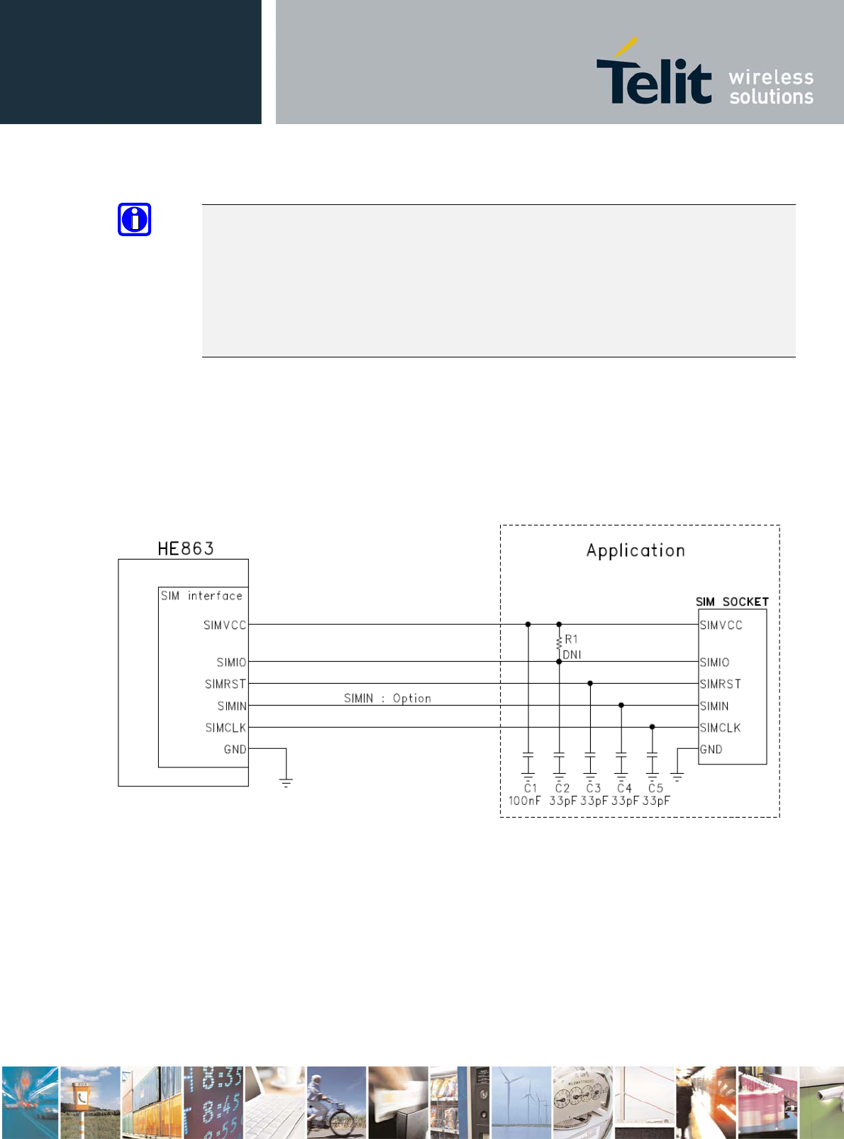
HE863 Family Hardware User Guide
1vv0300891 Rev.5- 2011-03-18
Reproduction forbidden without Telit Communications S.p.A’s. written authorization - All Rights
Reserved. Page 84 of 89
NOTE:
SIMIN doesn’t require any pull-up resistor. It is built in.
SIM card is detected inserted when this line is short to
ground.(TBD)
If in the application the SIM holder doesn’t foresee the
switch for the presence/absence of the SIM card, the SIMIN
line must be connected to ground.
15.2. SIM interface
When designing SIM interface on the application boards, the
following schematics are recommended.
3GPP specifications define that the rise time and the fall
time of the IO signal shall not exceed 1 usec.
R1 and C2 are very closely related to the rise and fall time
of the SIMIO signal.
It can differ according to application board therefore it
should be considered at the customer point of view.
It means that the values of R1,C1,C2,C3,C4,C5 may be necessary
to be optimized according to the application design.

HE863 Family Hardware User Guide
1vv0300891 Rev.5- 2011-03-18
Reproduction forbidden without Telit Communications S.p.A’s. written authorization - All Rights
Reserved. Page 85 of 89
Telit highly recommends that the customers should verify the
relating specification when they design.
But in general there will be no issue if above schematics were
made on the application board. All components are DNI but one
component should be reserved for each line because they may
need to debug in future.
HE863 Family modules already have internally 4.7kohm pull up
resistor on SIMIO line.
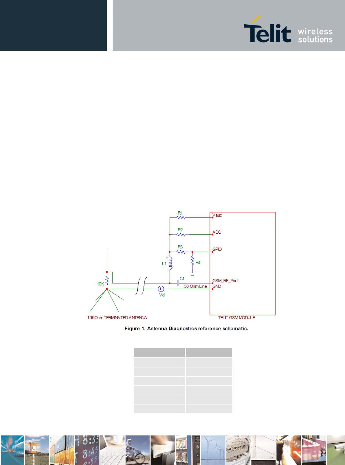
HE863 Family Hardware User Guide
1vv0300891 Rev.5- 2011-03-18
Reproduction forbidden without Telit Communications S.p.A’s. written authorization - All Rights
Reserved. Page 86 of 89
16. Antenna detection design guide
The following assumes that the application is using a commonly found 10KΩ
DC terminated antenna.
The figure below outlines the reference implementation, please keep in
mind that these components are in the RF path and care must be taken when
implementing this circuit.
The Vaux is a 1.8V regulated power source output from the module.
ADC is a 0 ~ 1200mV 10-bit Analog to Digital Converter input.
The software assumes the use of the ADC1 input and GPIO13 port of the
module for this purpose.
For the detailed operation of this function, please find AT#GSMAD command
in the HE863 AT Command Manual.
Component Value
R1 68KΩ
R2 15KΩ
R3 68KΩ
R4 68KΩ
L1 47nH
C1 33pF

HE863 Family Hardware User Guide
1vv0300891 Rev.5- 2011-03-18
Reproduction forbidden without Telit Communications S.p.A’s. written authorization - All Rights
Reserved. Page 87 of 89
17. Conformity Assessment Issues (TBD)
Information for the OEMs and Integrators
- HE863 Family modules are intended for the OEM integrator only.
- Please See the full Grant of Equipment document for other
restrictions.
- HE863 Family modules must be operated and used with a locally
approved access point.
Information to be supplied to the end user by the OEM or integrator
The following regulatory and safety notices must be published in
documentation supplied to the end user of the product or system
incorporating an adapter in compliance with local regulations.
Host system including HE863-NAD must be labeled with “Contains FCC
ID:RI7HE863NA”.
Host system including HE863-EUD must be labeled with “Contains FCC
ID:RI7HE863EU”.

HE863 Family Hardware User Guide
1vv0300891 Rev.5- 2011-03-18
Reproduction forbidden without Telit Communications S.p.A’s. written authorization - All Rights
Reserved. Page 88 of 89
18. Safety Recommendations
Read carefully!
Be sure about that the use of this product is allowed in your
country and in the environment required. The use of this product
may be dangerous and has to be avoided in the following areas:
Where it can interfere with other electronic devices in
environments such as hospitals, airports, aircrafts, etc.
Where there is risk of explosion such as gasoline stations,
oil refineries, etc.
It is responsibility of the user to enforce the country
regulation and the specific environment regulation.
Do not disassemble the product; any mark of tampering will
compromise the warranty validity.
We recommend following the instructions of the hardware user
guides for a correct wiring of the product. The product has to
be supplied with a stabilized voltage source and the wiring has
to be conforming to the security and fire prevention regulations.
The product has to be handled with care, avoiding any contact
with the pins because electrostatic discharges may damage the
product itself. Same cautions have to be taken for the SIM,
checking carefully the instruction for its use. Do not insert or
remove the SIM when the product is in power saving mode.
The system integrator is responsible of the functioning of the
final product; therefore, care has to be taken to the external
components of the module, as well as of any project or
installation issue, because the risk of disturbing the GSM
network or external devices or having impact on the security.
Should there be any doubt, please refer to the technical
documentation and the regulations in force.
Every module has to be equipped with a proper antenna with
specific characteristics. The antenna has to be installed with
care in order to avoid any interference with other electronic
devices and has to be installed with the guarantee of a minimum
20 cm distance from the body. In case of this requirement cannot
be satisfied, the system integrator has to assess the final
product against the SAR regulation.
The European Community provides some Directives for the
electronic equipments introduced on the market. All the relevant
information are available on the European Community website:
http://europa.eu.int/comm/enterprise/rtte/dir99-5.htm
HE863 Family Hardware User Guide
1vv0300891 Rev.5- 2011-03-18
Reproduction forbidden without Telit Communications S.p.A’s. written authorization - All Rights
Reserved. Page 89 of 89
The text of the Directive 99/05 regarding telecommunication
equipments is available, while the applicable Directives (Low
Voltage and EMC) are available at:
http://europa.eu.int/comm/enterprise/rtte/dir99-5.htm