Unication Co UNIGM601 GSM Module User Manual GM601 module V1 0
Unication Co Ltd GSM Module GM601 module V1 0
UserManual.wiki
>
Unication Co
>
UNIGM601 User Manual
User Manual
Navigation menu
Upload a User Manual
Namespaces
Wiki Guide
HTML
PDF
Info
Views
User Manual
Discussion / Help
Navigation
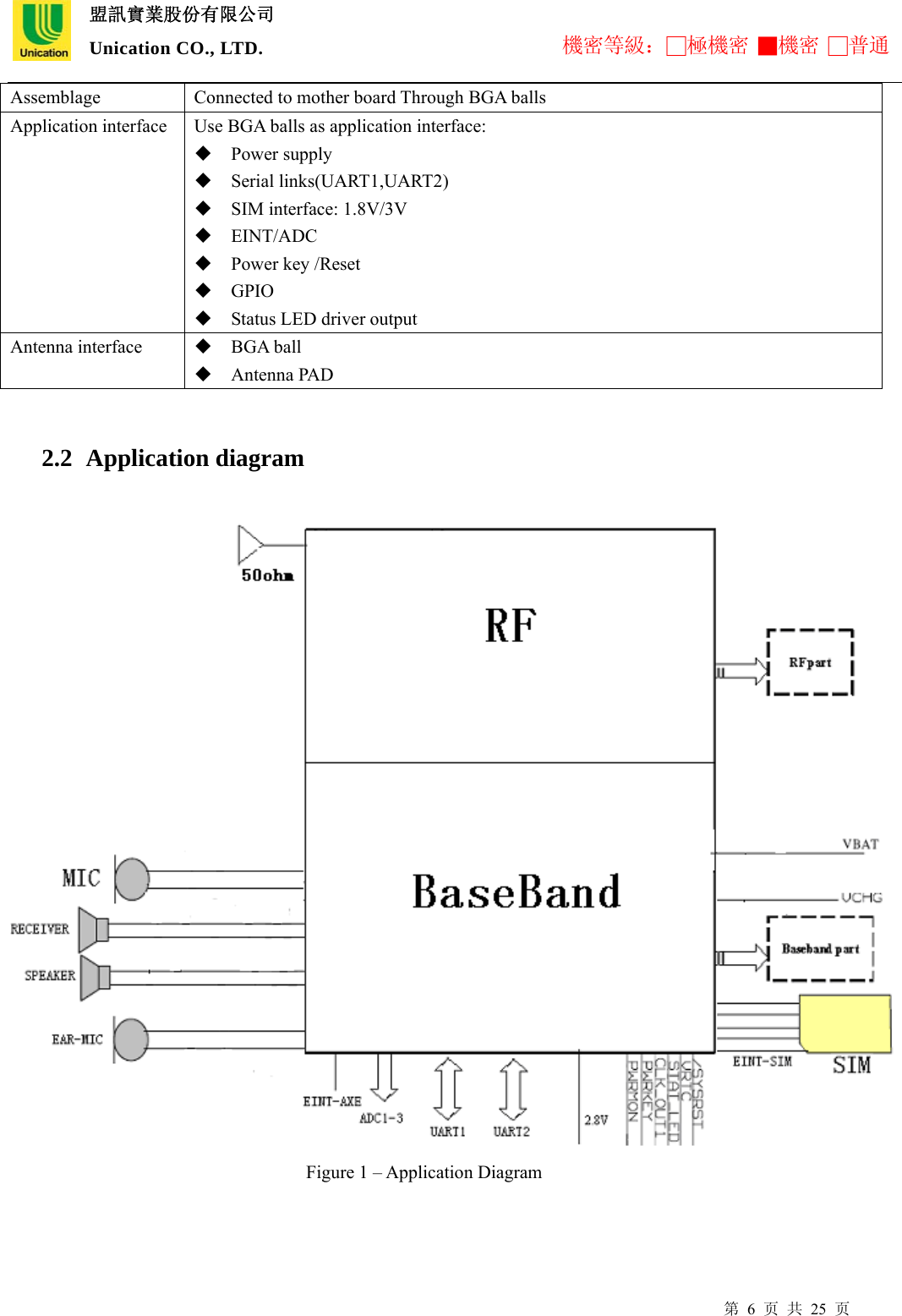
![盟訊實業股份有限公司 Unication CO., LTD. 機密等級:□極機密 ■機密 □普通 第 5 页 共 25 页 UART Universal Asynchronous Receiver-Transmitter VSWR Voltage Standing Wave Radio GPRS General Packet Radio Service FR Full Rate EFR Enhanced Full Rate HR Half Rate AP Applications Processor BB Baseband IMEI International Mobile Equipment Identity 1.6 Related documents [1] AT_Command_Set_For_GM601_V1.0 [2] GM601_module_BOM_V1.0 [3] GM601_module_EVB_User_Manual_V10 [4] Operation Description of GM601 Module_V1.0 2 GM601 Module introduction 2.1 Key feature GM601 is a self-contained GSM/GPRS quad-band(850/900/1800/1900) module including the following feature: Feature Implementation Power supply Single supply voltage:3.6~4.2V Power saving Typical power consumption in SLEEP mode less than 2.5mA(BS-PA-MFRMS=5) Frequency bands GM601 quad-band: GSM850,EGSM900,DCS1800,PCS1900 Compliant to GSM phase 2/2+ GSM class Small MS Transmitting power Class 4 (2W) at GSM850, EGSM900 Class 1(1W) at DCS1800, PCS1900 GPRS connectivity GPRS Class 12 capability:UL: 53.6 kbps/DL: 53.6 k Coding Scheme 1 – 4 Mobile station Class B Temperature range Normal operation: -10℃~+55℃; Restricted operation: -20℃~-10℃ and +55℃ ~ +65℃ Storage:-30℃ to 85℃ Audio interface Two groups of analog audio interfaces; one digital audio interface(DAI) Firmware upgrade Firmware upgraded over serial interface Real Time Clock Implemented](https://usermanual.wiki/Unication-Co/UNIGM601/User-Guide-1299429-Page-5.png)