Unication Co UNIGM601 GSM Module User Manual GM601 module V1 0
Unication Co Ltd GSM Module GM601 module V1 0
User Manual

盟訊實業股份有限公司
Unication CO., LTD. 機密等級:□極機密 ■機密 □普通
第 1 页 共 25 页
GM601 Module User Manual
Rev: V1.0
FCC Regulations:
This device complies with part 15 of the FCC Rules. Operation is subject to the following two conditions: (1) This
device may not cause harmful interference, and (2) this device must accept any interference received, including
interference that may cause undesired operation.
This device has been tested and found to comply with the limits for a Class B digital device, pursuant to Part 15 of the
FCC Rules. These limits are designed to provide reasonable protection against harmful interference in a residential
installation. This equipment generates, uses and can radiated radio frequency energy and, if not installed and used in
accordance with the instructions, may cause harmful interference to radio communications. However, there is no
guarantee that interference will not occur in a particular installation If this equipment does cause harmful interference
to radio or television reception, which can be determined by turning the equipment off and on, the user is encouraged to
try to correct the interference by one or more of the following measures:
-Reorient or relocate the receiving antenna.
-Increase the separation between the equipment and receiver.
-Connect the equipment into an outlet on a circuit different from that to which the receiver is connected.
-Consult the dealer or an experienced radio/TV technician for help.
Notice
The changes or modifications not expressly approved by the party responsible for compliance could void the user’s
authority to operate the equipment.

盟訊實業股份有限公司
Unication CO., LTD. 機密等級:□極機密 ■機密 □普通
第 2 页 共 25 页
Contents
1 Introduction ..............................................................................................................................................................4
1.1 Revision History............................................................................................................................................ 4
1.2 Purpose ..........................................................................................................................................................4
1.3 Scope ..............................................................................................................................................................4
1.4 Target audience............................................................................................................................................. 4
1.5 Abbreviations................................................................................................................................................ 4
1.6 Related documents........................................................................................................................................5
2 GM601 Module introduction...................................................................................................................................5
2.1 Key feature ....................................................................................................................................................5
2.2 Application diagram.....................................................................................................................................6
2.3 Package information..................................................................................................................................... 7
2.4 Pin define and description............................................................................................................................ 8
3 Module application description.............................................................................................................................12
3.1 Power supply ................................................................................................................................................12
3.3.1 Requirement...................................................................................................................................... 12
3.3.2 Power up sequence............................................................................................................................12
3.3.3 Power up mode .................................................................................................................................12
3.2 RF Antenna ...................................................................................................................................................12
3.3 Design rule for EMC ....................................................................................................................................13
3.4 Design rule for ESD......................................................................................................................................13
3.5 UART port and application........................................................................................................................... 14
3.5.1 UART function and parameter.......................................................................................................... 14
3.5.2 UART pin define...............................................................................................................................14
3.5.3 UART2 Typical application circuit ...................................................................................................15
3.6 Analogy Audio.............................................................................................................................................. 16
3.6.1 Interface define ................................................................................................................................. 16
3.6.2 Electro-acoustic devices reference specification .............................................................................. 17
3.7 SIM interface description and application .................................................................................................... 18
3.7.1 SIM interface define ......................................................................................................................... 18
3.7.2 SIM interface reference application circuit....................................................................................... 19
3.7.3 Design recommendation ...................................................................................................................19
3.8 GPIO description and application................................................................................................................. 19
3.8.1 GPIO description............................................................................................................................19
3.8.2 GPIO electrical characteristics......................................................................................................19
3.9 Mounting the GM601 on the Board..............................................................................................................21
3.9.1 General.............................................................................................................................................21
3.9.2 Module finish& Dimensions........................................................................................................... 21
3.9.3 Suggest Inhibit Area .......................................................................................................................21
3.9.4 Debug of the GM601 in Production ..............................................................................................22
3.9.5 Stencil............................................................................................................................................... 22
3.9.6 PCB Pad Design.............................................................................................................................. 22

盟訊實業股份有限公司
Unication CO., LTD. 機密等級:□極機密 ■機密 □普通
第 3 页 共 25 页
3.9.7 Solder Paste..................................................................................................................................... 24
3.9.8 Solder Reflow ..................................................................................................................................24
4 RF Exposure Information......................................................................................................................................25
盟訊實業股份有限公司
Unication CO., LTD. 機密等級:□極機密 ■機密 □普通
第 4 页 共 25 页
1 Introduction
1.1 Revision History
Revision Date Description
1.0 2010-6-9 Initial release
1.2 Purpose
This document describes the product design and specification for GM601. GM601 supports GSM/GPRS quad-band
(GSM850, EGSM900, DCS1800, and PCS1900).
1.3 Scope
This document describes: the platform architecture, the hardware/software interactions, Technical/Electrical
specifications.
1.4 Target audience
This document is intended to provide a design specification for the teams involved in and an introduction to the
platform for product integration teams.
1.5 Abbreviations
PPP Point-to-Point protocol
PSU Power Supply Unit
R&TTE Radio and Telecommunication Terminal Equipment
RAM Random Access Memory
SRAM Static Random Access Memory
NAND Not AND (electronic logic gate)
ROM Read-Only Memory
RMS Root Mean Square(value)
RTC Real Time Clock
Rx Receive Direction
Tx Transmit Direction
SAR Specific Absorption Rate
SIM Subscriber Identity Module
SMS Short Message Service
TA Terminal Adapter(e.g. GSM engine)
TDMA Time Division Multiple Access
TE Terminal Equipment, also referred to as DTE
盟訊實業股份有限公司
Unication CO., LTD. 機密等級:□極機密 ■機密 □普通
第 5 页 共 25 页
UART Universal Asynchronous Receiver-Transmitter
VSWR Voltage Standing Wave Radio
GPRS General Packet Radio Service
FR Full Rate
EFR Enhanced Full Rate
HR Half Rate
AP Applications Processor
BB Baseband
IMEI International Mobile Equipment Identity
1.6 Related documents
[1] AT_Command_Set_For_GM601_V1.0
[2] GM601_module_BOM_V1.0
[3] GM601_module_EVB_User_Manual_V10
[4] Operation Description of GM601 Module_V1.0
2 GM601 Module introduction
2.1 Key feature
GM601 is a self-contained GSM/GPRS quad-band(850/900/1800/1900) module including the following feature:
Feature Implementation
Power supply Single supply voltage:3.6~4.2V
Power saving Typical power consumption in SLEEP mode less than 2.5mA(BS-PA-MFRMS=5)
Frequency bands GM601 quad-band: GSM850,EGSM900,DCS1800,PCS1900
Compliant to GSM phase 2/2+
GSM class Small MS
Transmitting power Class 4 (2W) at GSM850, EGSM900
Class 1(1W) at DCS1800, PCS1900
GPRS connectivity GPRS Class 12 capability:UL: 53.6 kbps/DL: 53.6 k
Coding Scheme 1 – 4
Mobile station Class B
Temperature range Normal operation: -10℃~+55℃;
Restricted operation: -20℃~-10℃ and +55℃ ~ +65℃
Storage:-30℃ to 85℃
Audio interface Two groups of analog audio interfaces;
one digital audio interface(DAI)
Firmware upgrade Firmware upgraded over serial interface
Real Time Clock Implemented
盟訊實業股份有限公司
Unication CO., LTD. 機密等級:□極機密 ■機密 □普通
第 6 页 共 25 页
Assemblage Connected to mother board Through BGA balls
Application interface Use BGA balls as application interface:
Power supply
Serial links(UART1,UART2)
SIM interface: 1.8V/3V
EINT/ADC
Power key /Reset
GPIO
Status LED driver output
Antenna interface BGA ball
Antenna PAD
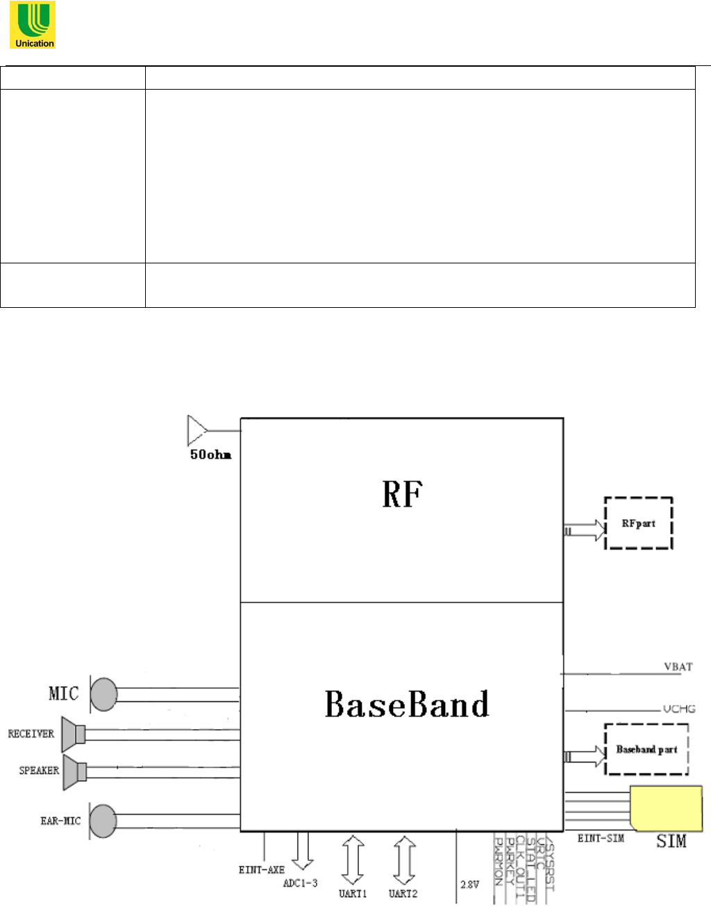
2.2 Application diagram
Figure 1 – Application Diagram
盟訊實業股份有限公司
Unication CO., LTD. 機密等級:□極機密 ■機密 □普通
第 7 页 共 25 页
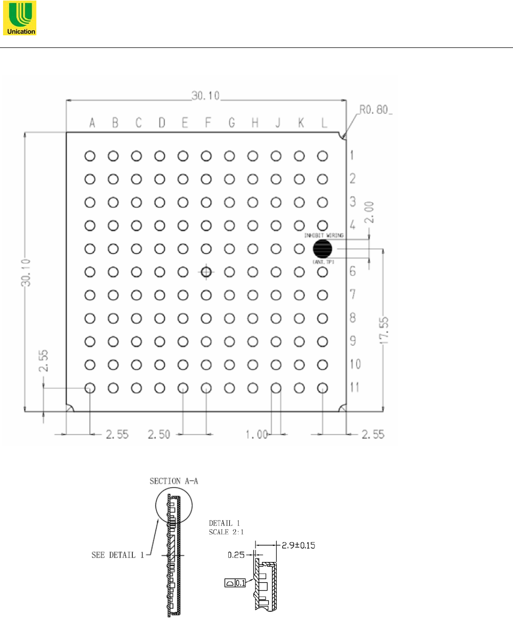
2.3 Package information
Figure2 – package and size
Figure3 - GM601 Side view of Package

盟訊實業股份有限公司
Unication CO., LTD. 機密等級:□極機密 ■機密 □普通
第 8 页 共 25 页
2.4 Pin define and description
Ball Signal I/O Function Pull
Up/Down Type
UART Interface
E7 C103/TXD I Serial data input (TXD) from DTE CMOS 2.8V
H8 C104/RXD O Serial data output to DTE CMOS 2.8V
B7 C108/DTR I Input for Data terminal ready signal (DTR) from DTE CMOS 2.8V
F7 C105/RTS I Input for Request to send signal (RTS) from DTE CMOS 2.8V
F6 C106/CTS O Output for Clear to send signal (CTS) to DTE CMOS 2.8V
D9 C109/DCD O Output for Data carrier detect signal (DCD) to DTE CMOS 2.8V
E11 C107/DSR O Output for Data set ready signal (DSR) to DTE CMOS 2.8V
B6 C125/RING O Output for Ring indicator signal (RI) to DTE CMOS 2.8V
SIM card interface
C10 SIMCLK O External SIM signal – Clock 1,8 / 3V
E9 SIMRST O External SIM signal – Reset 1,8 / 3V
D10 SIMIO I/O External SIM signal – Data I/O 1,8 / 3V
E11 SIMIN I External SIM signal – Presence (active low) 1,8 / 3V
D4 SIMVCC AO
External SIM signal – Power supply for the
SIM 1,8 / 3V
Debug Interface
D11 TX_TRACE O TX Data for debug monitor CMOS
2.8V
F10 RX_TRACE I RX Data for debug monitor CMOS
2.8V
Audio Interface
H9 EAR_MT- O Headset single end right channel audio
G10 EAR_MT+ O Headset single end left channel audio
H10 EAR_HF+ O Handset ear output, phase+ audio
J10 EAR_HF- O Handset ear output, phase- audio
J8 MIC_MT+ I Headset MIC. signal input: phase+ audio
G9 MIC_MT- I Headset MIC. signal input: phase- audio
G8 MIC_HF+ I Handset MIC. Input: phase+ audio
J9 MIC_HF- I Handset MIC. Input: phase- audio
F9 AXE I Handset switching CMOS
2.8V
DAC and ADC
C7 NC AO No defined /
J11 ADC_IN1 AI Analog/Digital converter input A/D
H11 ADC_IN2 AI Analog/Digital converter input A/D
G11 ADC_IN3 AI Analog/Digital converter input A/D

盟訊實業股份有限公司
Unication CO., LTD. 機密等級:□極機密 ■機密 □普通
第 9 页 共 25 页
Miscellaneous Functions
A2 RESET* I Reset input Power
E2 VRTC AI VRTC Backup Power
D8 STAT_LED AO Status indicator led OD
G1 CHARGE AI Charger input Power
G2 CHARGE AI Charger input Power
J5 ON_OFF* I Input command for switching power ON or
OFF (toggle command). Pull up to
VBATT
D5 VAUX1 AO Power output for external accessories Power
L8 PWRMON O Power ON Monitor CMOS
2.8V
L4 Antenna O Antenna output – 50 ohm RF
D7 DVI2_CLK - DVI2_CLK (Digital Voice Interface) CMOS
2.8V
GPIO
G4 TGPIO_12 I/O GPIO12 Configurable GPIO Pull Up CMOS
2.8V
C2 TGPIO_03 I/O GPIO03 Configurable GPIO Pull Down CMOS
2.8V
B3 TGPIO_04 I/O
GPIO04 Configurable GPIO / RF
Transmission Control Pull Down CMOS
2.8V
C3 TGPIO_20 I/O GPIO20 Configurable GPIO Pull Down CMOS
2.8V
B4 TGPIO_14 I/O GPIO14 Configurable GPIO Pull Up CMOS
2.8V
D1 TGPIO_11 I/O GPIO11 Configurable GPIO Pull Down CMOS
2.8V
B1 TGPIO_19 I/O GPIO19 Configurable GPIO Pull Up CMOS
2.8V
C1 TGPIO_01 I/O GPIO01 Configurable GPIO Pull Down CMOS
2.8V
K7 TGPIO_18 I/O
GPIO18 Configurable GPIO/ DVI2_RX
(Digital Voice Interface) Pull Up CMOS
2.8V
H5 TGPIO_17 I/O
GPIO17 Configurable GPIO /
DVI2_WA(Digital Voice Interface) Pull Up CMOS
2.8V
F5 TGPIO_15 I/O GPIO15 Configurable GPIO Pull Up CMOS
2.8V
K11 TGPIO_08 I/O GPIO08 Configurable GPIO Pull Down CMOS
2.8V
B5 TGPIO_06 /
ALARM I/O GPIO06 Configurable GPIO / ALARM Pull Down CMOS
2.8V
C9 TGPIO_09 I/O GPIO09 GPIO I/O pin Pull Up CMOS

盟訊實業股份有限公司
Unication CO., LTD. 機密等級:□極機密 ■機密 □普通
第 10 页 共 25 页
2.8V
E6 TGPIO_02 /
JDR I/O GPIO02 I/O pin Pull Down CMOS
2.8V
L9 TGPIO_07 /
BUZZER I/O GPIO07 Configurable GPIO / Buzzer Pull Down CMOS
2.8V
K10 TGPIO_13 I/O GPIO13 Configurable GPIO Pull Up CMOS
2.8V
K8 TGPIO_05 /
RFTXMON
I/O
GPIO05 Configurable GPIO / Transmitter
ON monitor Pull Down CMOS
2.8V
L10 TGPIO_21 I/O GPIO21 Configurable GPIO Pull Down CMOS
2.8V
E8 TGPIO_22 I/O GPIO22 Configurable GPIO Pull Up CMOS
2.8V
H3 TGPIO_10 I/O
GPIO10 Configurable GPIO / DVI2_TX
(Digital Voice Interface) Pull Up CMOS
2.8V
Power Supply
J1 VBATT - Main power supply Power
K1 VBATT - Main power supply Power
J2 VBATT - Main power supply Power
K2 VBATT - Main power supply Power
A1 GND - Ground Power
F1 GND - Ground Power
H1 GND - Ground Power
L1 GND - Ground Power
H2 GND - Ground Power
L2 GND - Ground Power
J3 GND - Ground Power
K3 GND - Ground Power
L3 GND - Ground Power
K4 GND - Ground Power
K5 GND - Ground Power
D6 GND - Ground Power
K6 GND - Ground Power
L6 GND - Ground Power
A11 GND - Ground Power
F11 GND - Ground Power
L11 GND - Ground Power
Reserved Pins
C4 -
C6 -
C5 -
C8 -

盟訊實業股份有限公司
Unication CO., LTD. 機密等級:□極機密 ■機密 □普通
第 11 页 共 25 页
D2 -
D3 -
A10 -
A3 -
A4 -
A5 -
A6 -
A7 -
A8 -
A9 -
B10 -
B11 -
B2 -
B8 -
B9 -
E1 -
E10 -
E3 -
E4 -
F2 -
F3 -
F4 -
F8 -
G5 -
G3 -
G6 -
G7 -
H4 -
H7 -
J4 -
J6 -
J7 -
K9 -
L5 -
E5 -
L7 -
H6

盟訊實業股份有限公司
Unication CO., LTD. 機密等級:□極機密 ■機密 □普通
第 12 页 共 25 页
3 Module application description
3.1 Power supply
3.3.1 Requirement
Input power voltage range: 3.6~4.2V;
Max Current: 2A;
Internal resistance<180mΩ
3.3.2 Power up sequence
Insert battery-> Pull down ON_OFF signal and hold more than 3 seconds-> start the module.
3.3.3 Power up mode
This module can be started by 3 ways:
Press ON_OFF signal;
Plug in charger and the module is auto started ;
Start by RTC
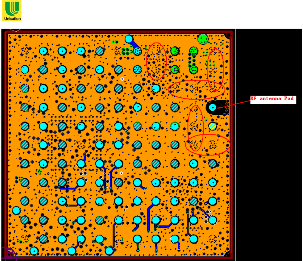
3.2 RF Antenna
Impedance of Signal connected to RF antenna pin should be 50ohm;
GND pins around RF antenna output pad should be well connected to mother board. It help to control impedance
and conducted hot from PA
The line connected to module’s RF antenna pad on the mother board should be routed as a strip line to help
controlling EMC and preventing the impendence acutely change
Pads of no connect define could be connected to GND to improve RF performances
盟訊實業股份有限公司
Unication CO., LTD. 機密等級:□極機密 ■機密 □普通
第 13 页 共 25 页
Figure4 – RF antenna Pad
3.3 Design rule for EMC
Please connect GND pins directly to motherboard GND, don’t through via or line;
Connect line between module power pins and battery connector on motherboard should be short and wide;
Add a 22uF and a 22pF capacitor close to battery connector;
Add a 1uF、a 100nF and a 22pF capacitor on charger connector.
3.4 Design rule for ESD
Add a zener Diode (ON SEMICON:NZL5V6ATT1G) at VBATT input port on motherboard;
Add a 1uF/16V capacitor at VCHG input port on motherboard;
Add TVS components on all audio channels.
盟訊實業股份有限公司
Unication CO., LTD. 機密等級:□極機密 ■機密 □普通
第 14 页 共 25 页
3.5 UART port and application
GM601 possesses of two UART ports: UART1 and UART2
3.5.1 UART function and parameter
UART1 function and parameter
PORT Wires used Baud
rate(bps)
Word length(bit) Parity Check Hardware
flow control
Function
UART1 RS232C 3-Wires 115200 8 No No Software
download and
debug
UART2 RS232C 9-wires 115200 8 No Yes Communication
with AP or PC
3.5.2 UART pin define
UART1 pin define (not include GND):
BGA Ball Name I/O Function Pull up/down Type
D11 TX_TRACE O Transmit data line Pull up CMOS 2.8V
F10 RX_TRACE I Receive data line Pull down CMOS 2.8V
UART2 pin define (not include GND):
BGA Ball Name I/O Function Pull up/down Type
E7 C103/TXD I DCE receive data line Pull up CMOS 2.8V
H8 C104/RXD O DCE transmit data line Pull up CMOS 2.8V
B7 C108/DTR I Data terminal ready(from DTE) Pull up CMOS 2.8V
F7 C105/RTS I Request to send (from DTE) Pull up CMOS 2.8V
F6 C106/CTS O Clear to send ( to DTE) Pull up CMOS 2.8V
D9 C109/DCD O Data carrier detect ( to DTE ) Pull up CMOS 2.8V
E11 C107/DSR O Data set ready ( to DTE) Pull up CMOS 2.8V
B6 C125/RING O Ring indicator (to DTE) Pull up CMOS 2.8V
盟訊實業股份有限公司
Unication CO., LTD. 機密等級:□極機密 ■機密 □普通
第 15 页 共 25 页
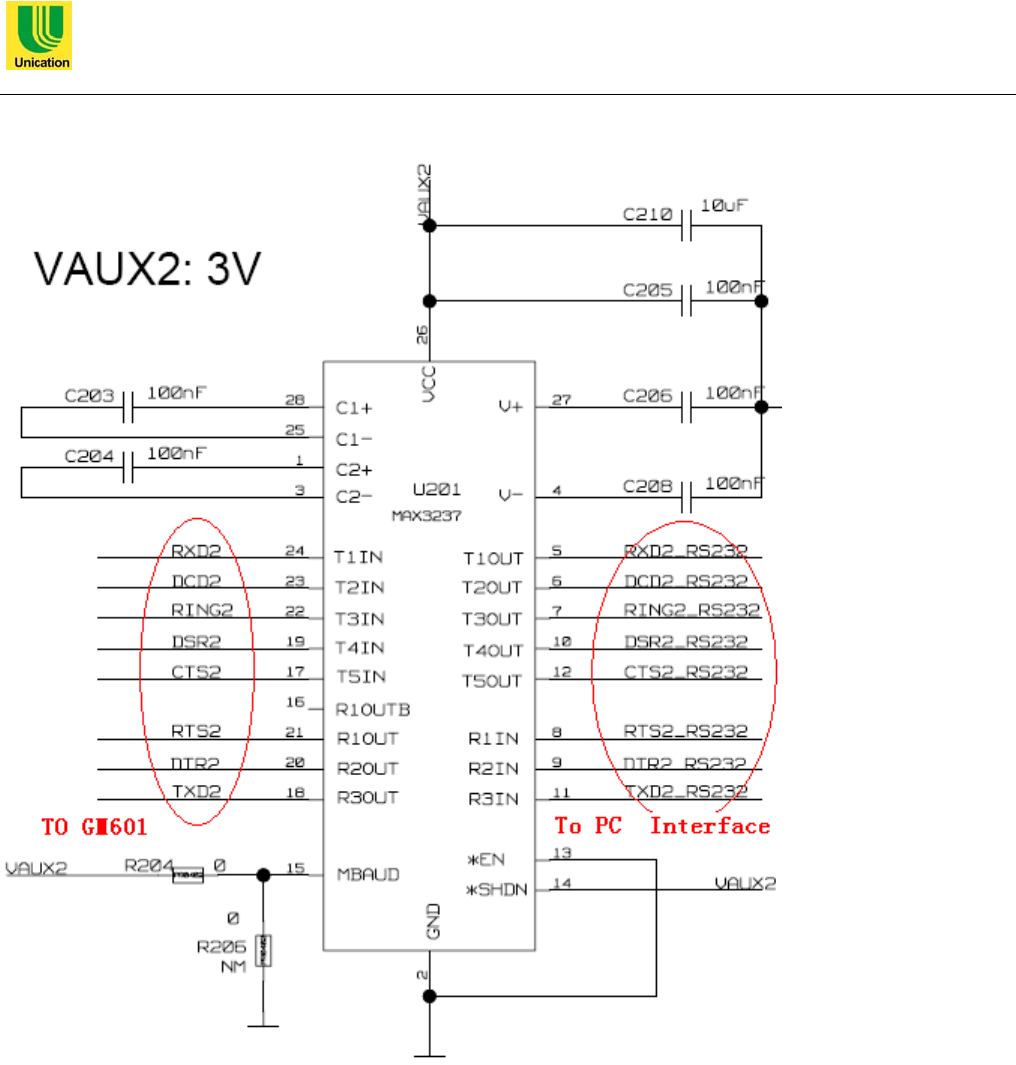
3.5.3 UART2 Typical application circuit
Figure 5 – UART2 typical application circuit 1
盟訊實業股份有限公司
Unication CO., LTD. 機密等級:□極機密 ■機密 □普通
第 16 页 共 25 页
Figure 6 – UART2 typical application circuit 1
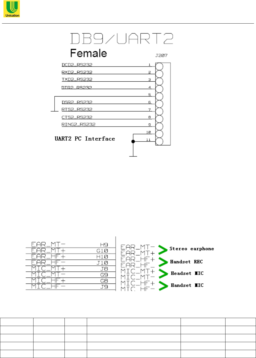
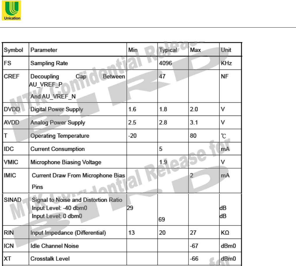
3.6 Analogy Audio
GM601 provide 4 audio channels: one for handset microphone, one for handset receiver, one for headset
earphone, one for headset microphone.
3.6.1 Interface define
Figure7 – Analogy audio interface
Audio pin define as follow (not include GND):
BGA BALL Name I/O Function Pull up/down Type
H9 EAR_MT- O Headset single end right channel audio
G10 EAR_MT+ O Headset single end left channel audio
H10 EAR_HF+ O Handset ear output, phase+ audio
J10 EAR_HF- O Handset ear output, phase- audio
盟訊實業股份有限公司
Unication CO., LTD. 機密等級:□極機密 ■機密 □普通
第 17 页 共 25 页
J8 MIC_MT+ I Headset MIC. signal input: phase+ audio
G9 MIC_MT- I Headset MIC. signal input: phase- audio
G8 MIC_HF+ I Handset MIC. Input: phase+ audio
J9 MIC_HF- I Handset MIC. Input: phase- audio
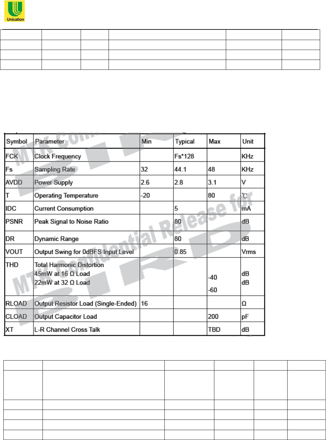
3.6.2 Electro-acoustic devices reference specification
We list the reference specification for engineers to choice electro-acoustic for GM601 module.
3.6.2.1 Stereo earphone
3.6.2.2 Handset receiver
Symbol Parameter Min Typical Max Unit
SINAD Signal to Noise and Distortion Ratio
Input Level: -40dBm0
Input Level: 0 dBm0
29
69
dB
dB
RLOAD Output Resistor Load (Differential) 28 Ω
CLOAD Output capacitor load 200 pF
ICN Idle channel noise of transmit path -67 dBm0
XT Crosstalk level on transmit path -66 dBm0
盟訊實業股份有限公司
Unication CO., LTD. 機密等級:□極機密 ■機密 □普通
第 18 页 共 25 页
3.6.2.3 Earphone microphone and handset microphone
3.7 SIM interface description and application
3.7.1 SIM interface define
SIM interface include 4 signals: SIMVCC,SIMRST,SIMCLK,SIMIO。Additionally, we define SIMIN
to indicate the SIM card’s inserting (low active)
SIM interface support 1.8V and 3V voltage and is auto identified according to SIM type.
盟訊實業股份有限公司
Unication CO., LTD. 機密等級:□極機密 ■機密 □普通
第 19 页 共 25 页
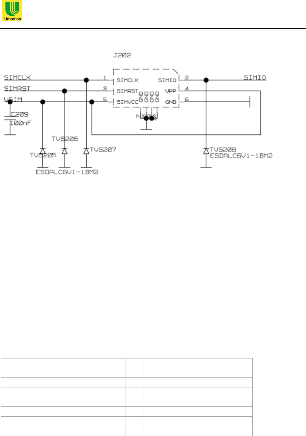
3.7.2 SIM interface reference application circuit
Figure 8 – SIM interface reference circuit
Note: recommend adding ESD components on every SIM signals.
3.7.3 Design recommendation
add ESD components on every SIM signals
SIMCLK is a 3.25MHZ clock signal and should be carefully treated with.
3.8 GPIO description and application
GPIOs (General Purpose I/Os) in GM601 are supplied by 2.8V voltage. GPIOs can be defined as input or
output mode and also can be multiplexed with other functionalities to reduce the pin number.
3.8.1 GPIO description
Reference to chapter 2.2 description about GPIOs
3.8.2 GPIO electrical characteristics
3.8.2.1 GPIO electrical characteristic correspond to CPU port
Signal CPU port Driving (mA) Pull PU/PD resistor (Kohm)
(Min, typical, max) Cin (pF)
TGPIO_12 GPIO1 max 16, min 2 PD 40, 75, 190 5.2
TGPIO_03 GPIO2 max 16, min 2 PD 40, 75, 190 5.2
TGPIO_04 GPIO3 max 16, min 2 PD 40, 75, 190 5.2
TGPIO_20 GPIO4 max 16, min 2 PD 40, 75, 190 5.2
TGPIO_14 GPIO5 max 16, min 2 PD 40, 75, 190 5.2
TGPIO_11 GPIO6 max 16, min 2 PD 40, 75, 190 5.2

盟訊實業股份有限公司
Unication CO., LTD. 機密等級:□極機密 ■機密 □普通
第 20 页 共 25 页
TGPIO_19 GPIO7 max 16, min 2 PD 40, 75, 190 5.2
TGPIO_01 GPIO11 max 16, min 2 PD 40, 75, 190 5.2
TGPIO_18 GPIO17 6 PU 40, 75, 190 5.2
TGPIO_17 GPIO19 6 PU 40, 75, 190 5.2
TGPIO_15 GPIO18 6 PU 40, 75, 190 5.2
TGPIO_08 GPIO8 max 16, min 2 PD 40, 75, 190 5.2
TGPIO_06 GPIO24 4 PD 40, 75, 190 5.2
TGPIO_09 GPIO9 max 16, min 2 PD 40, 75, 190 5.2
TGPIO_02 GPIO10 max 16, min 2 PD 40, 75, 190 5.2
TGPIO_07 GPIO28 2 PU 40, 75, 190 5.2
TGPIO_16
TGPIO_13 GPIO13 max 16, min 2 PD 40, 75, 190 5.2
TGPIO_05 GPIO12 max 16, min 2 PD 40, 75, 190 5.2
TGPIO_21 GPIO25 4 PD 40, 75, 190 5.2
TGPIO_22 GPIO22 2 PU 5.2
TGPIO_10 GPIO16 6 PD 40, 75, 190 5.2
3.8.2.2 GPIO Absolute Maximum Ratings
Item Symbol Min Max Unit
IO power supply VDD33 -0.3 VDD33+0.3 V
IO Input voltage VDD33I -0.3 VDD33+0.3 V
Operating temperature Topr -20 80 Celsius
Storage temperature Tstg -55 125 Celsius
Remark: VDD33=2.8V
3.8.2.3 GPIO logic level ratings
Levels Min Max Unit
Input low level - 0.8 V
Input high level 2.0 - V
Output low level - 0.4 V
Output high level 2.4 - V
盟訊實業股份有限公司
Unication CO., LTD. 機密等級:□極機密 ■機密 □普通
第 21 页 共 25 页
3.9 Mounting the GM601 on the Board
3.9.1 General
The GM601 modules have been designed in order to be compliant with a standard lead-free SMT
process.
3.9.2 Module finish& Dimensions
Figure 9 –Module finish&Dimensions
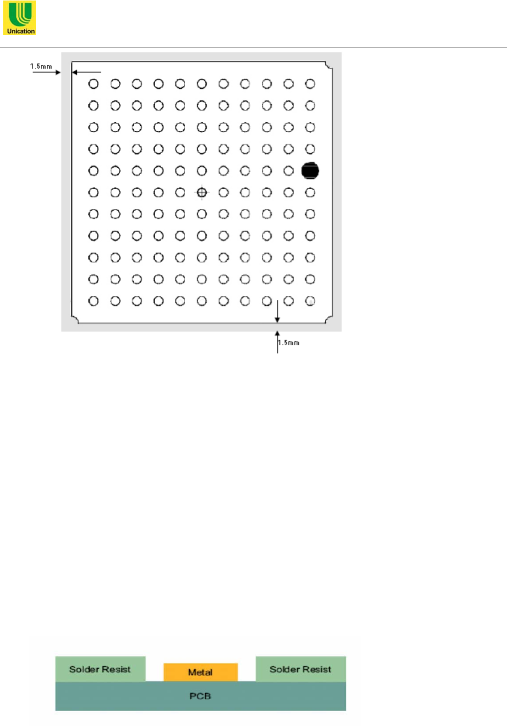
3.9.3 Suggest Inhibit Area
In order to easily rework the GM601 is suggested to consider on the application a 1.5mm inhibit area
around the module.
盟訊實業股份有限公司
Unication CO., LTD. 機密等級:□極機密 ■機密 □普通
第 22 页 共 25 页
Figure 10 –Suggest Inhibit Area
3.9.4 Debug of the GM601 in Production
To test and debug the mounting of the GM601, we strongly recommend to foreseen test pads on the
host PCB, in order to check the connection between the GM601 itself and the application and to test the performance of
the module connecting it with an external computer. Depending by the customer application, these pads include, but are
not limited to the following signals:
• TXD
• RXD
• ON/OFF
• RESET
• GND
• VBATT
• TX_TRACE
• RX_TRACE
• PWRMON
3.9.5 Stencil
Stencil’s apertures layout can be the same of the recommended footprint (1:1), we suggest a
thickness of stencil foil ≥ 120μm.
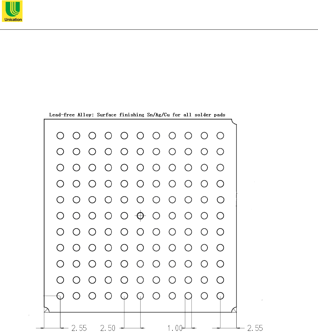
3.9.6 PCB Pad Design
Non solder mask defined type is recommended for the solder pads on the PCB.
盟訊實業股份有限公司
Unication CO., LTD. 機密等級:□極機密 ■機密 □普通
第 23 页 共 25 页
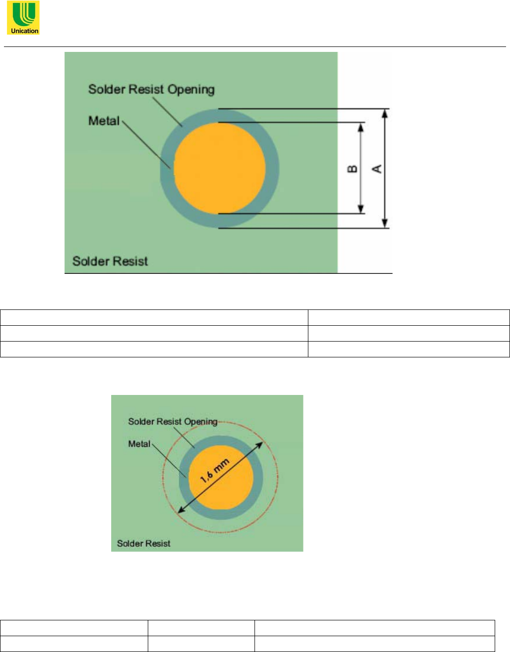
Figure 11 –PCB pad design
Recommendation for PCB pad dimensions:
Ball pitch(mm) 2.5
Solder resist opening diameter A (mm) 1.150
Metal pad diameter B (mm) 1+/-0.05
It is recommended no microvia without solder resist cover under the module and no microvia around the pads
(see following figure):
Figure 12 –microvia without solder resist cover area
Holes in pad are allowed only for blind holes and not for through holes.
Recommendations for PCB pad surfaces:
Finish Layer thickness(um) Properties
Electro-less Ni/Immersion Au 3-7/0.05-0.15 Good solder ability protection, high shear force values
The PCB must be able to resist the higher temperatures which are occurring at the lead-free process.
盟訊實業股份有限公司
Unication CO., LTD. 機密等級:□極機密 ■機密 □普通
第 24 页 共 25 页
3.9.7 Solder Paste
Lead free
Solder paste Sn/Ag/Cu
3.9.8 Solder Reflow
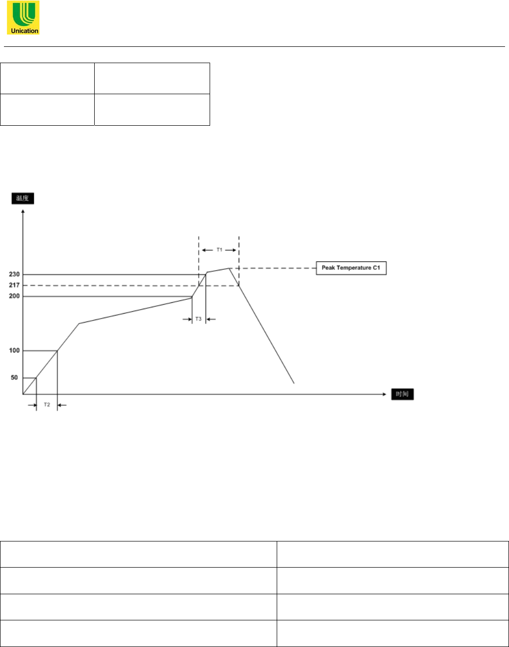
Recommend classification reflow profile:
Figure13 – Classification Reflow Profile
Table 4-1
Notes:
Parameters requirement described is only suitable for lead-free process.
Lead-free process means:Use Lead-free alloy Solder paste (for example 95.5Sn3.0Ag0.5Cu) .
All temperature refers to top side of the package. Measured on the package body surface:
Peak temperature C1 235℃~255℃
Time above 220℃ T1 30~75s
Time between 50℃ and 100℃ T2 >16s
Time between 220℃ and 235℃ T3 >5s

盟訊實業股份有限公司
Unication CO., LTD. 機密等級:□極機密 ■機密 □普通
第 25 页 共 25 页
4 RF Exposure Information
This device meets the government’s requirements for exposure to radio waves.
This device is designed and manufactured not to exceed the emission limits for exposure to radio frequency (RF)
energy set by the Federal Communications Commission of the U.S. Government.
This device complies with FCC radiation exposure limits set forth for an uncontrolled environment. In order to avoid
the possibility of exceeding the FCC radio frequency exposure limits, human proximity to the antenna shall not be less
than 20cm (8 inches) during normal operation.
Maximum antenna gain allowed for use with this device is GSM850 3.8 dBi,GSM1900 2.4 dBi.
When the module is installed in the host device, the FCC ID label must be visible through a window on the final device
or it must be visible when an access panel, door or cover is easily re-moved. If not, a second label must be placed on
the outside of the final device that contains the following text: “Contains FCC ID: LEAUNIGM601”