Universal Scientific UNA-P3 3G Module User Manual PDD TG SOM RA01
Universal Scientific Industrial Co., Ltd. 3G Module PDD TG SOM RA01
User manual

Doc. Title UNA Plus/ UNA-Lite Function EVB User
Guide
Originator Max Shu
Date 2013.10.29
Version V1.2
Product Line UMD (MPC)
Doc. NO.
CONFIDENTIAL Low ;Normal High
The information contained herein is the exclusive property of Universal Scientific Industrial Co., Ltd. and shall not be
distributed, reproduced, or disclosed in whole or in part without prior written permission of USI Co., Ltd.

Revision Record
Version Revise content Date
1.1 Initial Release 2013.06.06
The information contained herein is the exclusive property of Universal Scientific Industrial Co., Ltd. and shall not be distributed,
reproduced, or disclosed in whole or in part without prior written permission of USI Co., Ltd. 頁1

Category
1. FCC Regulations ....................................................................................3
2. R&TTE Regulations ..............................................................................4
3. RF Exposure Information......................................................................5
4. Information of Installed Module...........................................................6
5. Illustration of Function EVB.................................................................7
6. General Mode.........................................................................................9
6-1 Setting of Jumpers & Switches .............................................................9
7. Settings for Download /Update Mode.................................................14
8. Advance Mode......................................................................................15
8-1 Module on/off Control...........................................................................15
8-2 Voltage Settings....................................................................................15
8-3 Use External Power Supplier...............................................................16
8-4 Current Measurement...........................................................................17
8-5 Settings for Slide-Style Switch (J42)...................................................17
8-6 PCM Signal ............................................................................................18
8-6-1 PCM Signal Port (J24)................................................................................................................... 18
8-6-2 PCM Loop Settings........................................................................................................................ 19
8-6-3 External I2C Interface to Control Audio Codec .............................................................................. 20
8-7 UART0 & UART1 Signal Port (J23)......................................................21
8-8 Wakeup Control ....................................................................................22
8-8-1 USB Mode ..................................................................................................................................... 22
8-8-2 USB+UART Mode ......................................................................................................................... 23
The information contained herein is the exclusive property of Universal Scientific Industrial Co., Ltd. and shall not be distributed,
reproduced, or disclosed in whole or in part without prior written permission of USI Co., Ltd. 頁2
1. FCC Regulations
z This device complies with part 15 of the FCC Rules. Operation is subject to the
following two conditions: (1) This device may not cause harmful interference, and
(2) this device must accept any interference received, including interference that
may cause undesired operation.
z This device has been tested and found to comply with the limits for a Class B
digital device, pursuant to Part 15 of the FCC Rules. These limits are designed to
provide reasonable protection against harmful interference in a residential
installation. This equipment generates, uses and can radiated radio frequency
energy and, if not installed and used in accordance with the instructions, may cause
harmful interference to radio communications. However, there is no guarantee that
interference will not occur in a particular installation If this equipment does cause
harmful interference to radio or television reception, which can be determined by
turning the equipment off and on, the user is encouraged to try to correct the
interference by one or more of the following measures:
Reorient or relocate the receiving antenna.
Increase the separation between the equipment and receiver.
Connect the equipment into an outlet on a circuit different from that to
which the receiver is connected.
Consult the dealer or an experienced radio/TV technician for help.
The maximum antenna gain for frequency 900 is 2 dBi; for frequency 1800 is
2 dBi ;and the antenna separation distance is 20cm.
Maximum antenna gain allowed for use with this device is 2 dBi.
Changes or modifications not expressly approved by the party responsible for
compliance could void the user‘s authority to operate the equipment.
The information contained herein is the exclusive property of Universal Scientific Industrial Co., Ltd. and shall not be distributed,
reproduced, or disclosed in whole or in part without prior written permission of USI Co., Ltd. 頁3

2. R&TTE Regulations
In all cases assessment of the final product must be mass against the Essential
requirements of the R&TTE Directive Articles 3.1(a) and (b), safety and EMC
respectively, as well as any relevant Article 3.3 requirements.
1. Health (Article 3.1(a) of the R&TTE Directive)
Applied Standard(s):
EN62311:2008
2. Safety (Article 3.1(a) of the R&TTE Directive)
Applied Standard(s):
EN 60950-1:2006/A11:2009/A1:2010/A12:2011
3. Electromagnetic compatibility (Article 3.1 (b) of the R&TTE Directive)
Applied Standard(s):
EN 301 489-1 V1.9.2/-7 V1.3.1/-24 V1.5.1
4. Radio frequency spectrum usage (Article 3.2 of the R&TTE Directive)
Applied Standard(s):
EN 301 511 V9.0.2
EN 301 908-1 V5.2.1/ -2 V5.2.1
The information contained herein is the exclusive property of Universal Scientific Industrial Co., Ltd. and shall not be distributed,
reproduced, or disclosed in whole or in part without prior written permission of USI Co., Ltd. 頁4
3. RF Exposure Information
Radiation Exposure Statement:
This equipment complies with FCC radiation exposure limits set forth for an uncontrolled
environment. This equipment should be installed and operated with minimum distance 20cm between
the radiator & your body.
This device is intended only for OEM integrators under the following conditions:
1) The antenna must be installed such that 20 cm is maintained between the antenna and users
2) The transmitter module may not be co-located with any other transmitter or antenna.
As long as 2 conditions above are met, further transmitter test will not be required. However, the
OEM integrator is still responsible for testing their end-product for any additional compliance
requirements required with this module installed
IMPORTANT NOTE: In the event that these conditions can not be met (for example certain laptop
configurations or co-location with another transmitter), then the FCC authorization is no longer
considered valid and the FCC ID can not be used on the final product. In these circumstances, the
OEM integrator will be responsible for re-evaluating the end product (including the transmitter) and
obtaining a separate FCC authorization.
End Product Labeling
This transmitter module is authorized only for use in device where the antenna may be installed such
that 20 cm may be maintained between the antenna and users. The final end product must be labeled
in a visible area with the following: “Contains FCC ID: IXM-UNA-P3”. The grantee's FCC ID can
be used only when all FCC compliance requirements are met.
Manual Information To the End User
The OEM integrator has to be aware not to provide information to the end user
regarding how to install or remove this RF module in the user’s manual of the end
product which integrates this module.
The end user manual shall include all required regulatory information/warning as show in this
manual.
The information contained herein is the exclusive property of Universal Scientific Industrial Co., Ltd. and shall not be distributed,
reproduced, or disclosed in whole or in part without prior written permission of USI Co., Ltd. 頁5
1) The antenna must be installed such that 20 cm is maintained between the antenna and users,
and the maximum antenna gain allowed for use with this device is 2dBi.
2) The transmitter module may not be co-located with any other transmitter or antenna.
4. Information of Installed Module
Module Name UNA-P3/UNA-L3
HW Version V21
SW Version V2.4.00101
GSM Band 850, 900, 1800, 1900
UMTS Band FDD I, FDD II, FDD V
GSM Feature R99
GPRS Class 12
EDGE Class 12
UMTS Feature HSDPA, HSUPA,HSPA+(R7)
AT Command 3GPP TS 27.007, 27.005
SIM/USIM Support 3V and 1.8V
Interface USB 2.0 high speed
Operating Temperature Frequency Stability covers operating
temperature range of -20° to +50°C
Operating Voltage 3.4 ~ 4.2V
The information contained herein is the exclusive property of Universal Scientific Industrial Co., Ltd. and shall not be distributed,
reproduced, or disclosed in whole or in part without prior written permission of USI Co., Ltd. 頁6
User Guide for UNA PLUS Function EVB
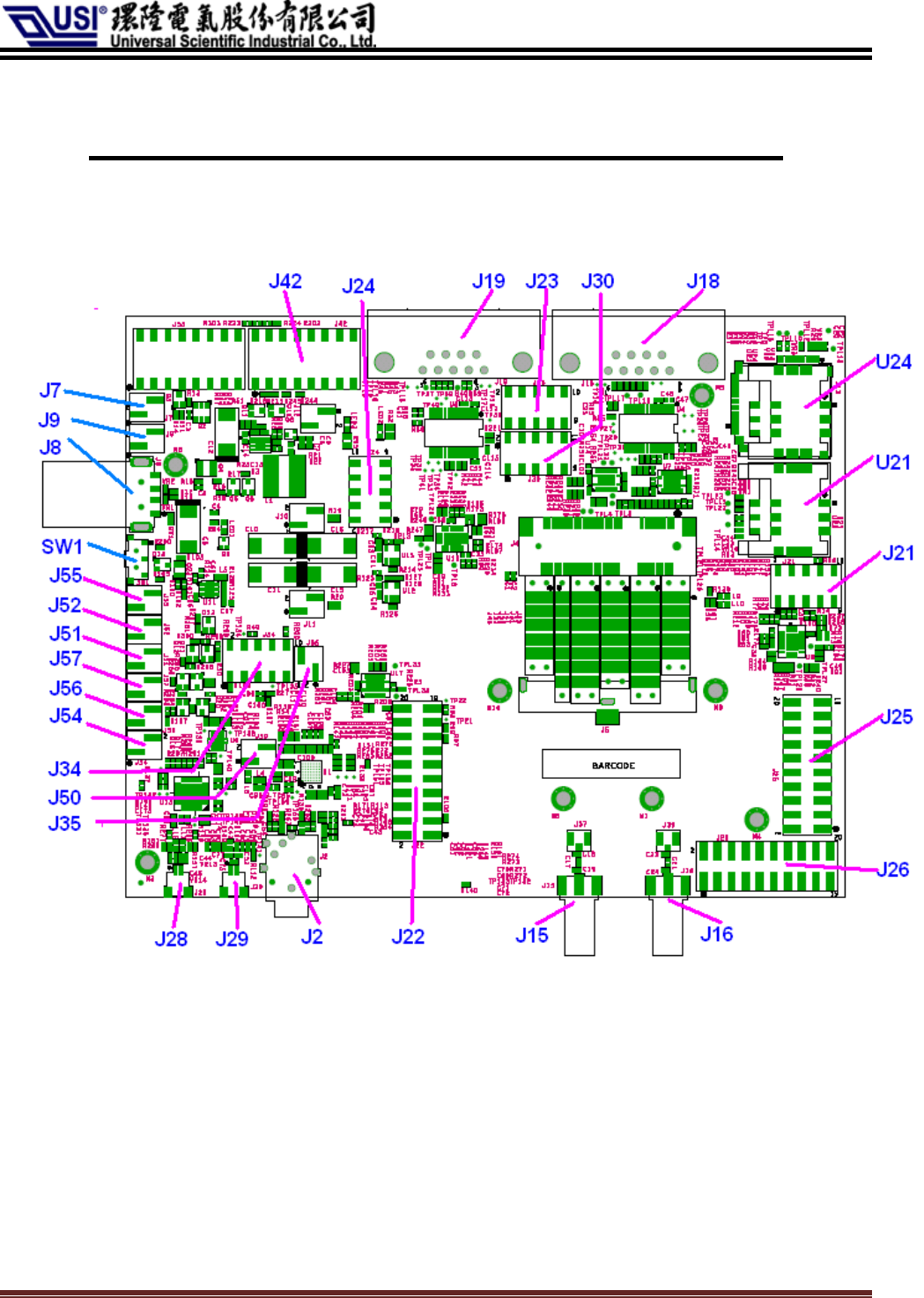
5. Illustration of Function EVB
Figure. Layout of Function EVB
The information contained herein is the exclusive property of Universal Scientific Industrial Co., Ltd. and shall not be distributed,
reproduced, or disclosed in whole or in part without prior written permission of USI Co., Ltd. 頁7
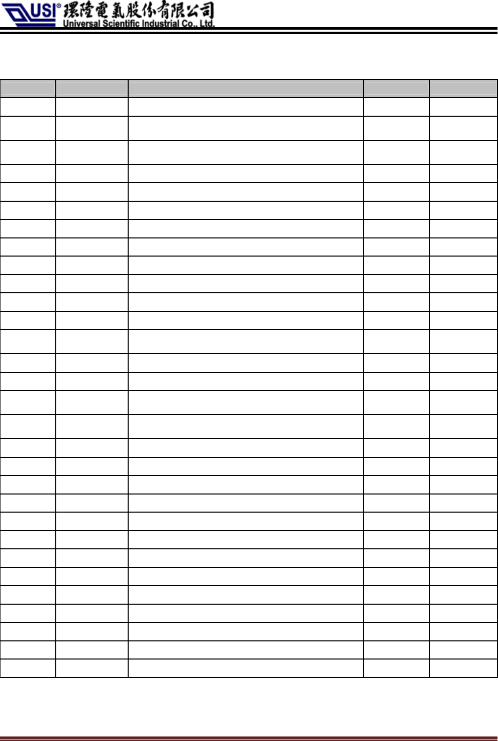
Reference Type Description Support Non-Support
J8 USB Conn. Connect host PC or download firmware V
J7 Pin Header Select external power supplier (+)
(Default is ‘Open’.) V
J9 Pin Header Select external power supply (-)
(Default is ‘Open’.) V
SW1 On/off switch Module on/off control V
J55 Pin Header Module on/off control (Default is ‘Open’.) V
J15 Ant. Conn. Main antenna SMA Connector V
J16 Ant. Conn. AUX antenna SMA Connector V
U24 SIM 1 Conn. Connect SIM Card V
U21 SIM 2 Conn. Connect SIM Card V
J18 COM port 0 Debug Pin V
J19 COM port 1 Transmit/ Receive AT Command. V
J21 Pin Header Factory Test (Default is ‘Open’.) V
J23 Pin Header UART0 & UART1 signal connector
(Default is ‘Open’.) V
J30 Pin Header Factory Test (Default is ‘Open’.) V
J24 Pin Header PCM signal connector (Default is ‘Open’.) V
J56 Pin Header Wake up AP in AP sleep mode
(wake up AP) (Default is ‘Open’.) V
J54 Pin Header Wake up module in module sleep mode
(wake up modem) (Default is ‘Open’.) V
J2 Headset Conn. EAR PHONE & MIC V
J28 Audio Conn. Audio LINE-OUT V
J29 Audio Conn. Audio LINE-IN V
J42 Switch Conn. Slide-Style Switch. V
J52 Pin Header Factory Test (Default is ‘Open’.) V
J51 Pin Header Factory Test (Default is ‘Open’.) V
J57 Pin Header Factory Test (Default is ‘Open’.) V
J34 Pin Header Factory Test (Default is ‘Open’.) V
J35 Pin Header Factory Test (Default is ‘Open’.) V
J50 Pin Header Factory Test (Default is ‘Open’.) V
J22 Pin Header Factory Test (Default is ‘Open’.) V
J25 Pin Header Factory Test (Default is ‘Open’.) V
J26 Pin Header Factory Test (Default is ‘Open’.) V
The information contained herein is the exclusive property of Universal Scientific Industrial Co., Ltd. and shall not be distributed,
reproduced, or disclosed in whole or in part without prior written permission of USI Co., Ltd. 頁8
6. General Mode
6-1 Setting of Jumpers & Switches
Step7
Step6
Step5 Step4
Step2
Step8
Step3
Figure. Settings of general mode
Step1. Remove every jumper on the board.
The information contained herein is the exclusive property of Universal Scientific Industrial Co., Ltd. and shall not be distributed,
reproduced, or disclosed in whole or in part without prior written permission of USI Co., Ltd. 頁9

Step2. Keep ‘R19’ and ‘R20’ short.
R20
R19
Figure. Keep ’R19’ and ‘R20’ short.
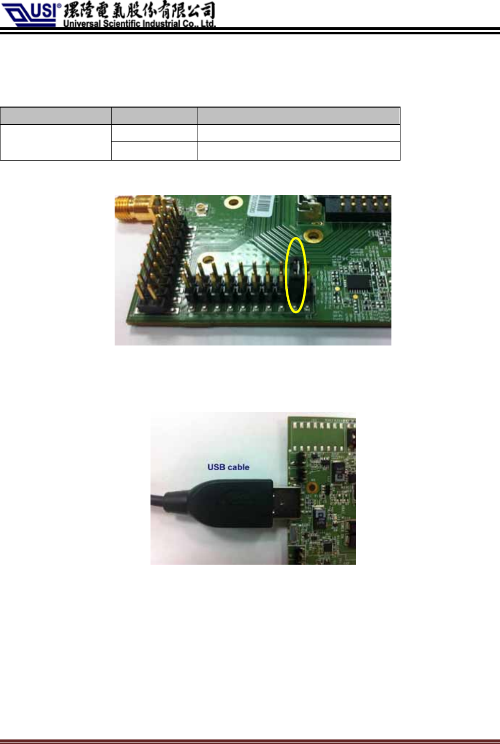
Step3. For ‘SW1’, select 1-2. (Upper position)
Figure. For ‘SW1’, select 1-2.
Step4. For ‘J42’, eight switches should be in ‘OFF’ position.
OFF
ON
Figure. Switches in ‘OFF’ position.
The information contained herein is the exclusive property of Universal Scientific Industrial Co., Ltd. and shall not be distributed,
reproduced, or disclosed in whole or in part without prior written permission of USI Co., Ltd. 頁10
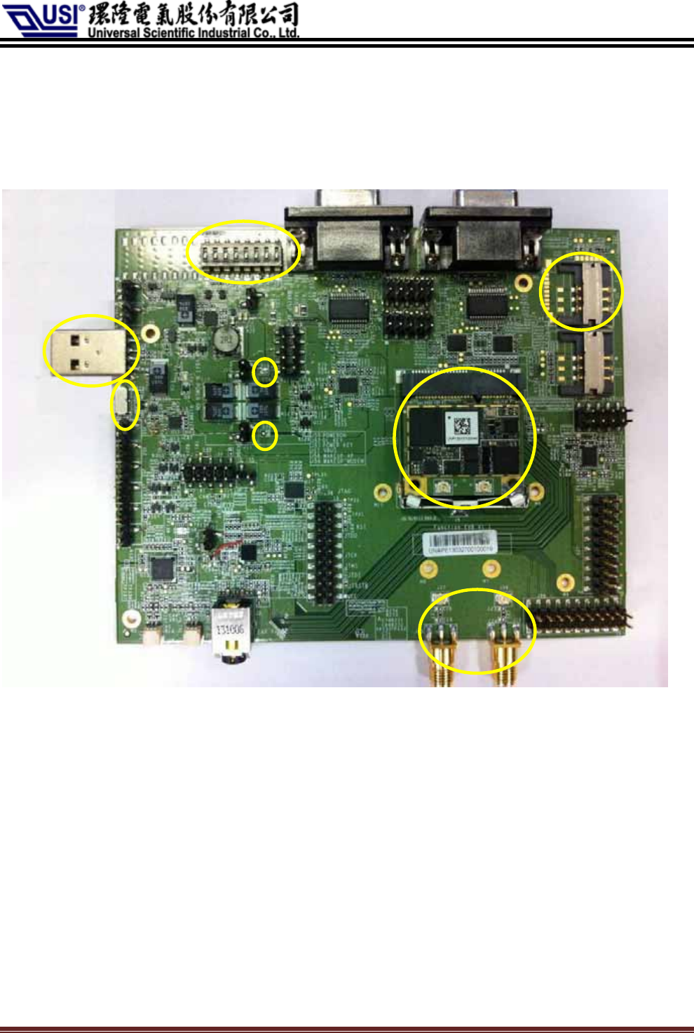
Step5. Insert SIM card.
Figure. Insert correctly SIM card.
Step6. Set up Antenna.
a. Connect bottom of mini card by U.FL cable as following photo.
Figure. Connect by U.FL cable.
b.Connect EVB and mini card by U.FL cable. Put mini card on EVB.
Figure. Connect mini card and EVB.
The information contained herein is the exclusive property of Universal Scientific Industrial Co., Ltd. and shall not be distributed,
reproduced, or disclosed in whole or in part without prior written permission of USI Co., Ltd. 頁11

b. Connect SMA antenna.
Figure. Connect antenna.
Step7. Set up Module.
an mini card and insert it on the socket, J4.
b. Press mini card until it is stuck
a. By 30 degree angle, le
Figure. Insert mini card.
by connector, J5.
Figure. Mini card is stuck.
The information contained herein is the exclusive property of Universal Scientific Industrial Co., Ltd. and shall not be distributed,
reproduced, or disclosed in whole or in part without prior written permission of USI Co., Ltd. 頁12
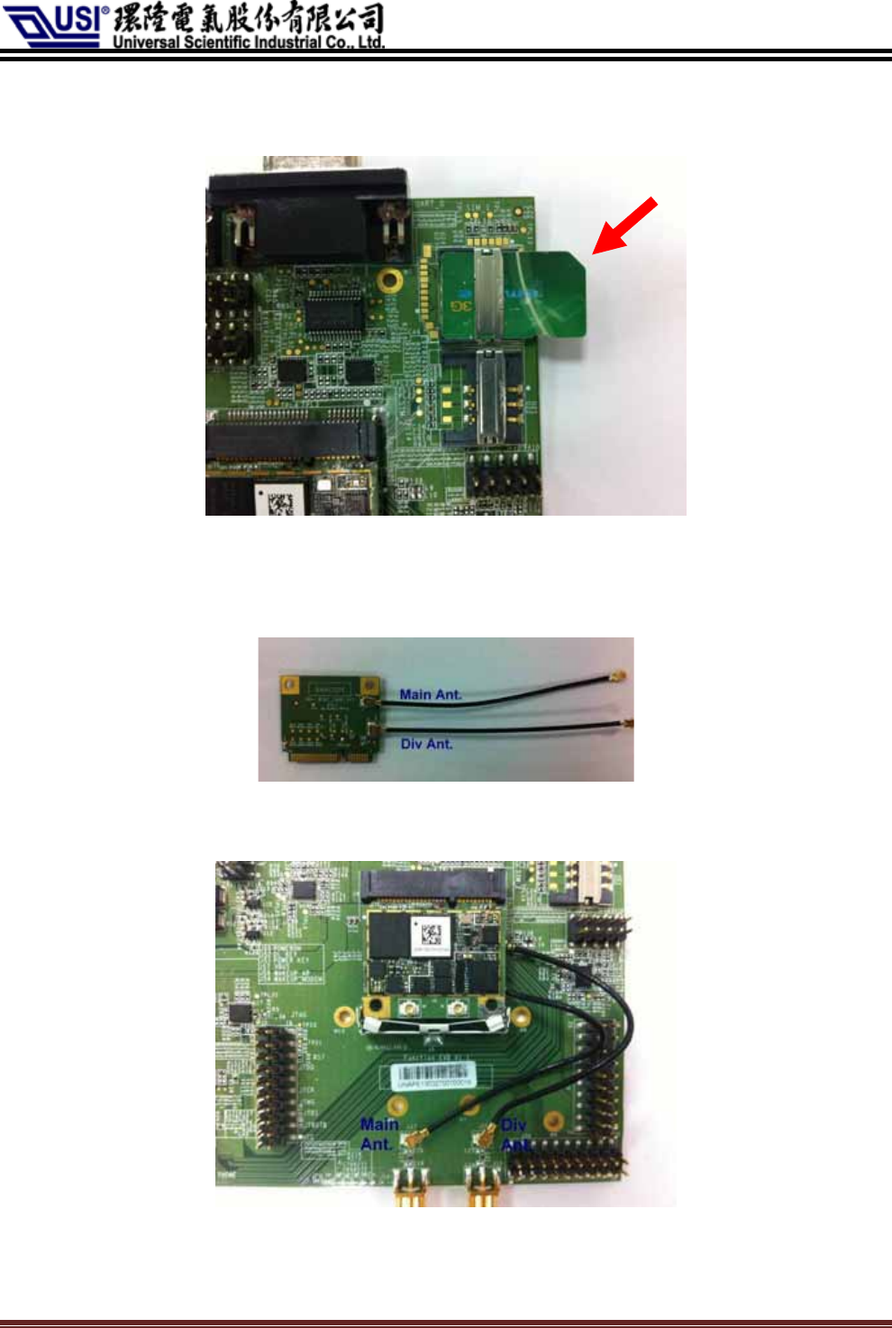
tep8. Connect computer by USB cable.
n 60 mm.
S
Recommended USB cable length is less tha
Figure. Connect PC by USB cable.
The information contained herein is the exclusive property of Universal Scientific Industrial Co., Ltd. and shall not be distributed,
reproduced, or disclosed in whole or in part without prior written permission of USI Co., Ltd. 頁13
7. Settings for Download /Update Mode
Component reference Open/Short Function
Open Close Download/Update mode
Pin17-18 in J25 Short Start Download/Update mode
Step1. Put back the jumper in J25 to short its Pin.17, Pin.18.
Figure. Put back jumper.
Step2. Connect EVB and computer by USB cable.
Figure. Connect PC.
Step3. About SW part, please refer to the file, ‘UNA PLUS Flash Tool User Guide’.
The information contained herein is the exclusive property of Universal Scientific Industrial Co., Ltd. and shall not be distributed,
reproduced, or disclosed in whole or in part without prior written permission of USI Co., Ltd. 頁14
8. Advance Mode
8-1 Module on/off Control
a. Method 1. Module Control by SW1.
Component reference Function SW1,1-2 SW1,2-3
SW1 Control Module Turn on (Default) Turn off
PS2. Please remove the Jump, J55, at first.
b. Method 2. Module Control by J55.
Component reference Open/Short Function
Open Shut down (Default)
J55 Short Turn on
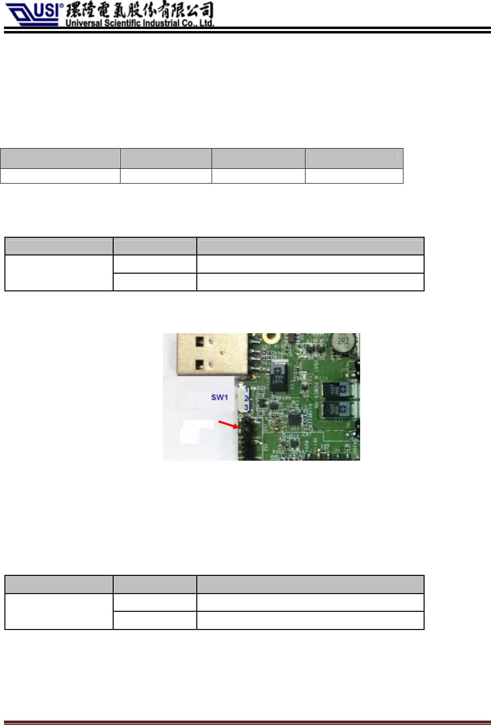
PS3. Please select 2-3 for SW1 at first. (Lower position)
J55
Figure. J55 & SW1
8-2 Voltage Settings
Component reference Open/Short Function
Open Supply 3.3Volt to 3G Module. (Default)
J12 Short Supply 4.35Volt to 3G Module.
The information contained herein is the exclusive property of Universal Scientific Industrial Co., Ltd. and shall not be distributed,
reproduced, or disclosed in whole or in part without prior written permission of USI Co., Ltd. 頁15
8-3 Use External Power Supplier
Please follow the steps as below.
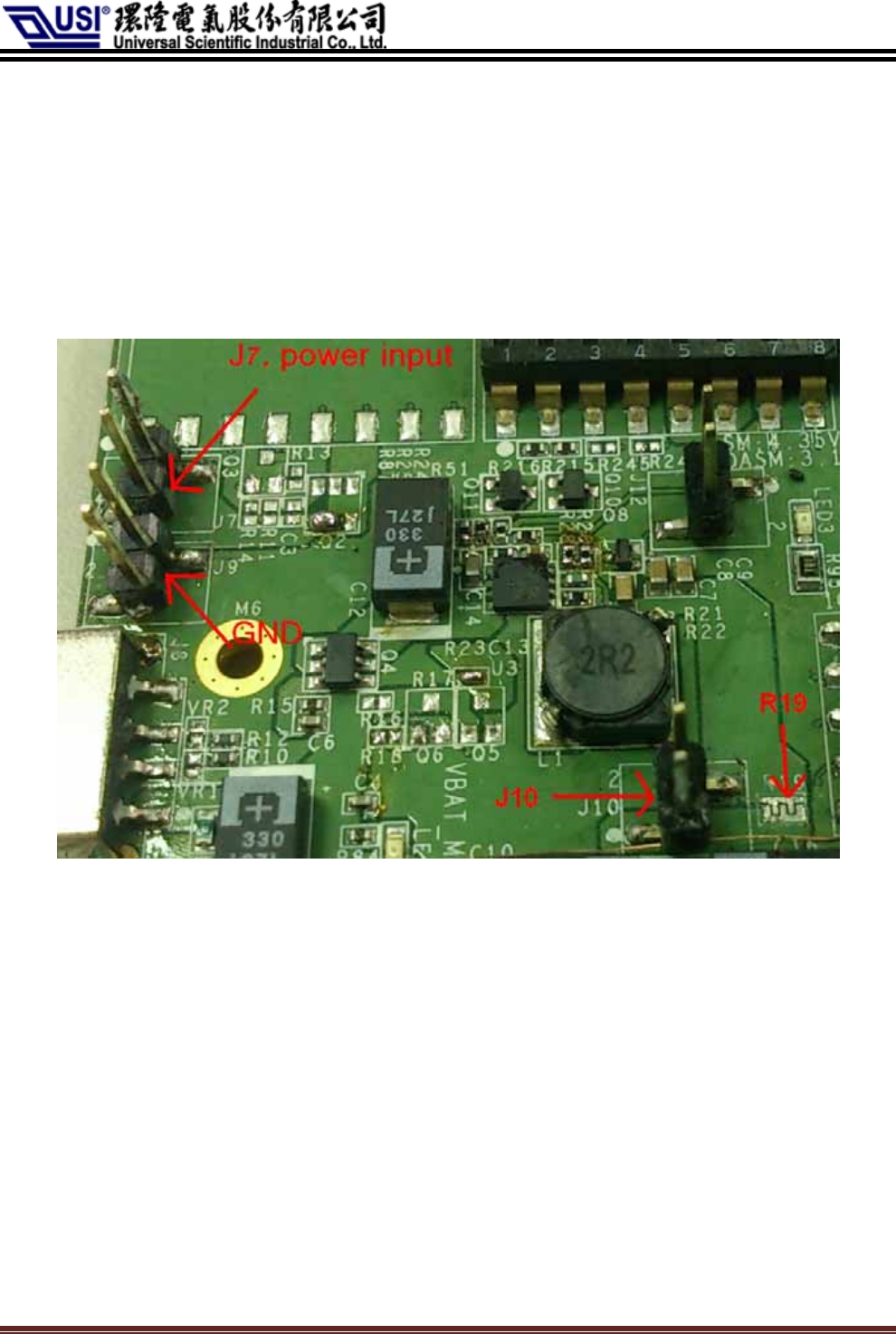
Step1. Remove the jumper, J10 and clear solder on R19.
Step2. Connect host PC by USB cable.
Step3. J7 is power input, and voltage range is from 3.3V to 4.3V.
Step4. J9 is GND.
Figure. J7, J9, J10 & J19
The information contained herein is the exclusive property of Universal Scientific Industrial Co., Ltd. and shall not be distributed,
reproduced, or disclosed in whole or in part without prior written permission of USI Co., Ltd. 頁16
8-4 Current Measurement
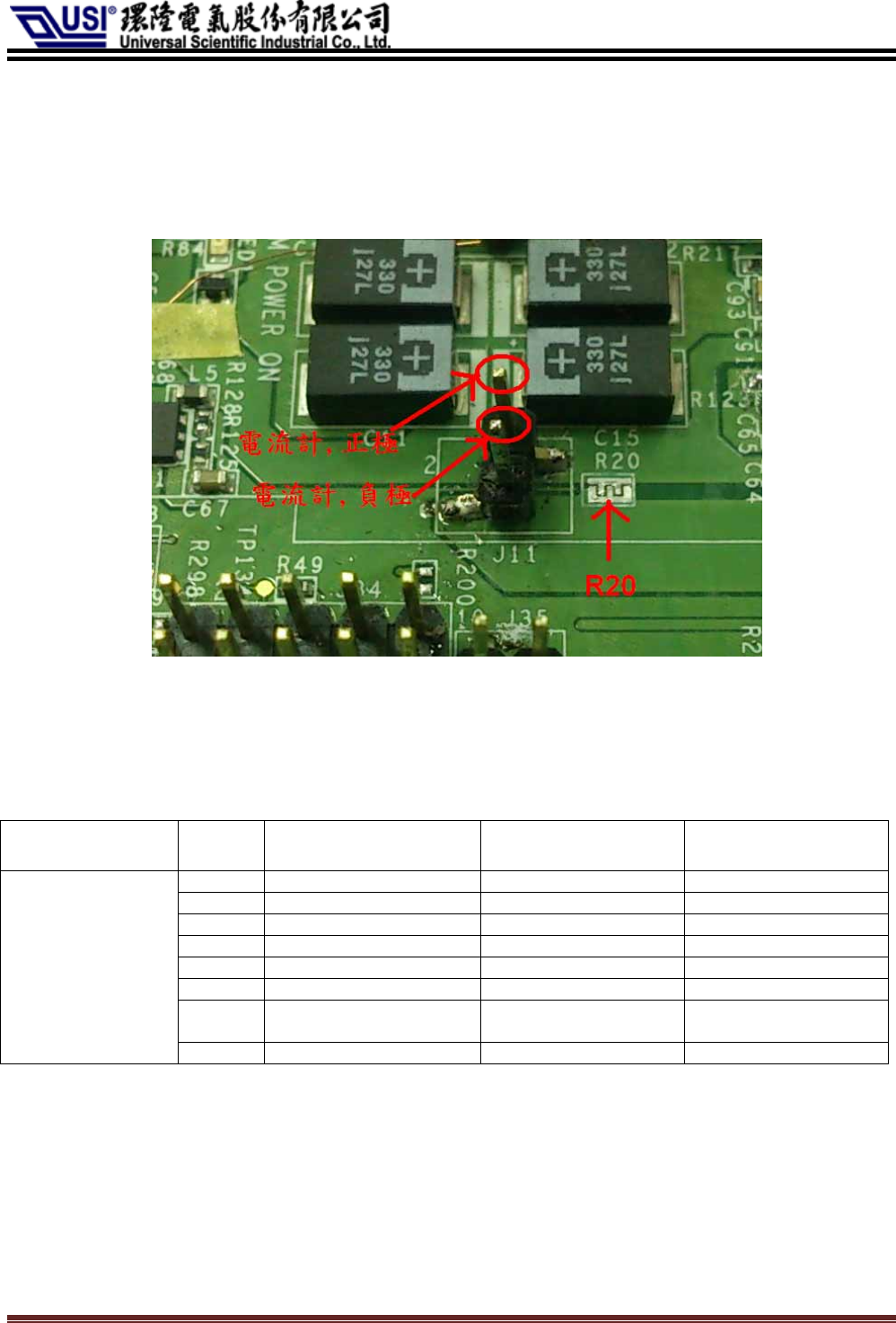
Step1. Clear solder on R20.
Step2. Measure two sides of J11.
Figure. R20, J11
8-5 Settings for Slide-Style Switch (J42)
Component
reference Group Function OFF (Default) ON
1 Factory Test V
2 Factory Test V
3 Factory Test V
4 Factory Test V
5 Control UART0 (J18) Open UART0 port Close UART0 port
6 Control UART1 (J19) Open UART1 port Close UART1 port
7 PCM signal select Import to internal Audio
codec Export to external
connector. (J24)
J42
8 Factory Test V
In general mode, these eight switches should be set in ‘OFF’ position.
The information contained herein is the exclusive property of Universal Scientific Industrial Co., Ltd. and shall not be distributed,
reproduced, or disclosed in whole or in part without prior written permission of USI Co., Ltd. 頁17
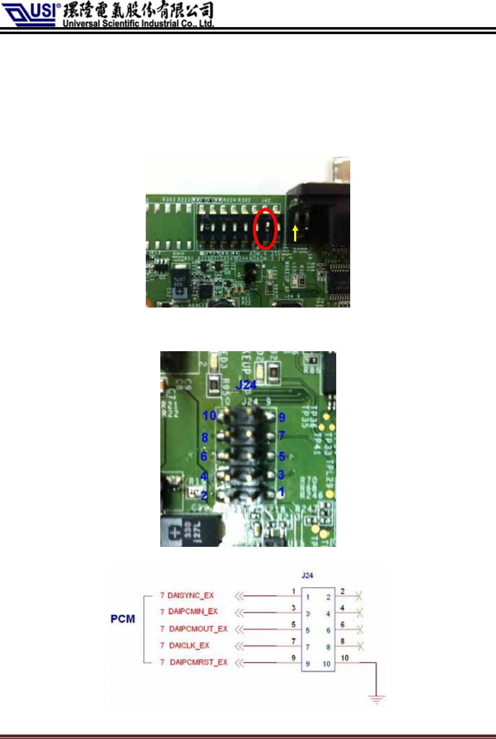
8-6 PCM Signal
8-6-1 PCM Signal Port (J24)
Step1. Group.7 switch in J42 should be in ‘ON’ position as follows.
Step2. Please refer to the following photo to connect ‘J24’.
The information contained herein is the exclusive property of Universal Scientific Industrial Co., Ltd. and shall not be distributed,
reproduced, or disclosed in whole or in part without prior written permission of USI Co., Ltd. 頁18
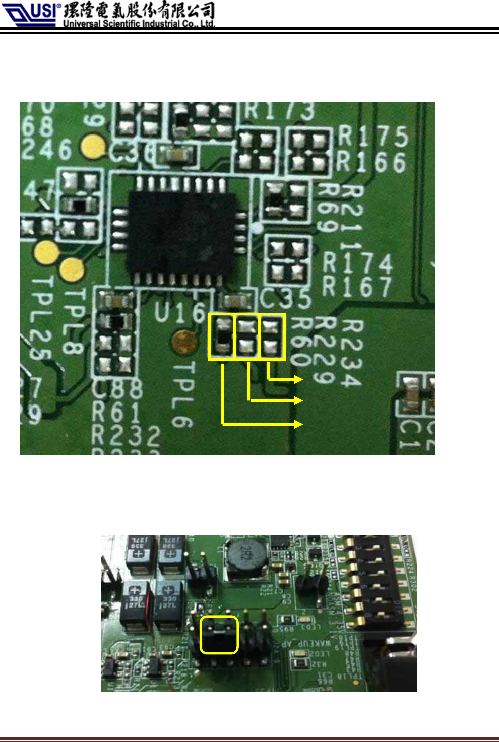
Step3. Then, please confirm signal level. Default setting is 1.8V. If you’d like 2.8V
or 3.3V, please rework EVB by referring to following photos.
R60:1.8V(Default)
R229:2.8V
R234:3.3V
Figure. R20, J11
8-6-2 PCM Loop Settings
Step1. Please follow 8-6-1.
Step2. Put back the jumper in J24 to short its Pin.3 and Pin.5.
Figure. J24
The information contained herein is the exclusive property of Universal Scientific Industrial Co., Ltd. and shall not be distributed,
reproduced, or disclosed in whole or in part without prior written permission of USI Co., Ltd. 頁19

8-6-3 External I2C Interface to Control Audio Codec
Step1. Group.7 switch in J42 should be in ‘OFF’ position as follows.
Figure. J42
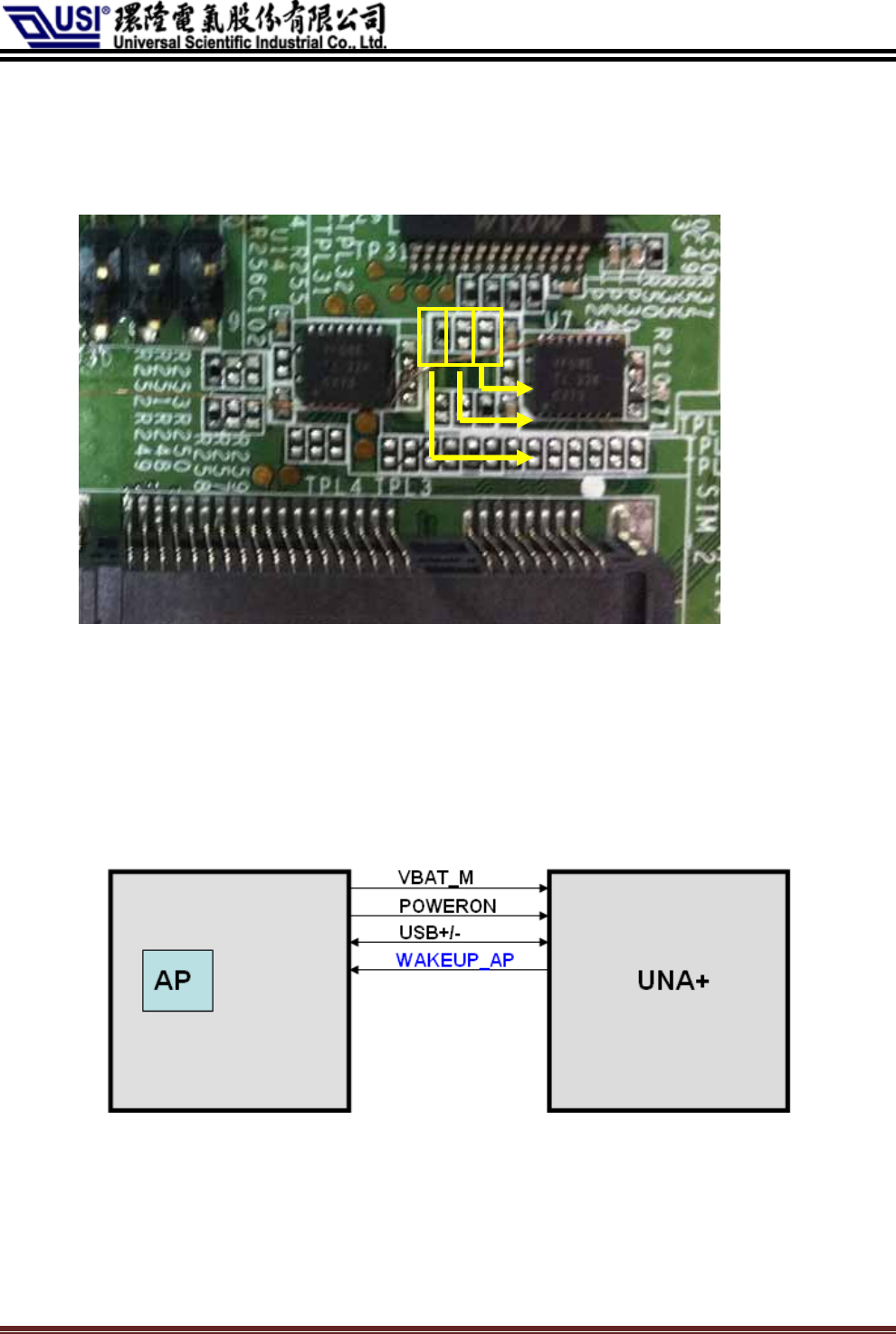
Step2. AP could control modem by ‘J25’. J25.8 is SCL. J25.10 is SDA. Voltage
level is 1.8V.
SCL SDA
Figure. J25
Step3. About Codec init table, please refer to the file, ‘UNA PLUS EVB Codec
ReaTtek ALC5637Q Initial Table’.
The information contained herein is the exclusive property of Universal Scientific Industrial Co., Ltd. and shall not be distributed,
reproduced, or disclosed in whole or in part without prior written permission of USI Co., Ltd. 頁20
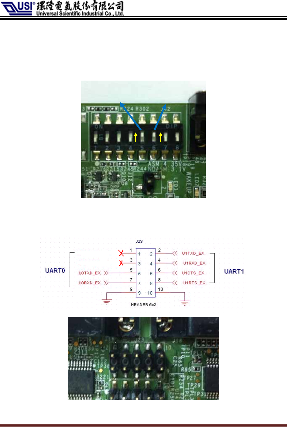
8-7 UART0 & UART1 Signal Port (J23)
Step1. Group.5 (for UART0) & Group.6 (for UART1) switches in J42 should be in
‘ON’ position.
UART0 UART1
Figure. Group5&6 switches in J42
Step2. Please refer to the following photo to connect ‘J23’.
2 4 6 8 10
1357 9
Figure. Pin definition of J23
The information contained herein is the exclusive property of Universal Scientific Industrial Co., Ltd. and shall not be distributed,
reproduced, or disclosed in whole or in part without prior written permission of USI Co., Ltd. 頁21
Step3. Please confirm signal level. Default setting is 3.3V. If you’d like 1.8V or 2.8V,
please refer to the following photo to rework the EVB. Please put back
‘R241’ (default setting) before you use UART0 (J18) and UART1 (J19).
R242:1.8V
R239:2.8V
R241:3.3V(Default)
Figure. Voltage adjustment for UART.
8-8 Wakeup Control
8-8-1 USB Mode
Please comply with the following procedures, from step 1 to step 3.
Figure. USB Mode
The information contained herein is the exclusive property of Universal Scientific Industrial Co., Ltd. and shall not be distributed,
reproduced, or disclosed in whole or in part without prior written permission of USI Co., Ltd. 頁22
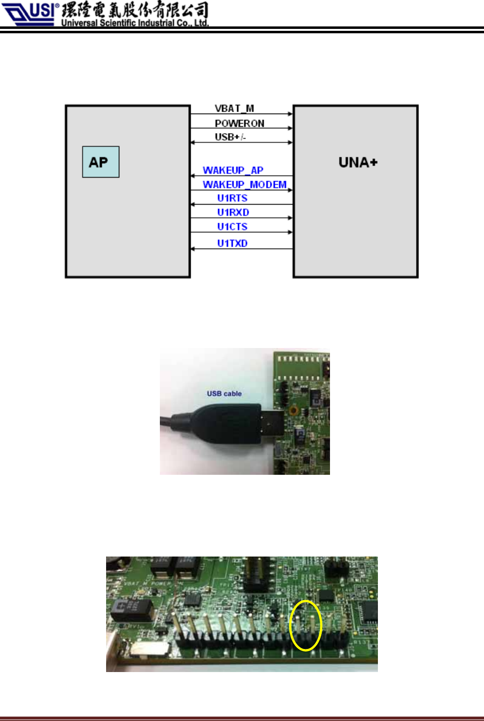
8-8-2 USB+UART Mode
Please comply with the following procedures, from step 1 to step 5.
Figure. USB+UART Mode
Operation Procedure
Step1. Connect EVB & Host/AP by USB cable.
Figure. Connect Host/AP & EVB
Step2. Please refer to Section 4-1, ‘Module on/off control’, to start up modem.
Step3. Connect AP/Host and EVB by ‘J56’, Signal ‘WAKEUP AP’. Voltage level is
1.8V.
Figure. J56, Signal ‘WAKEUP AP’
The information contained herein is the exclusive property of Universal Scientific Industrial Co., Ltd. and shall not be distributed,
reproduced, or disclosed in whole or in part without prior written permission of USI Co., Ltd. 頁23
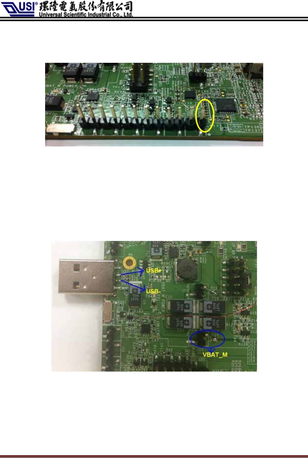
Step4. Connect AP/Host and EVB by ‘J54.1’, Signal ‘WAKEUP MODEM’.
Voltage level is 1.8V. ‘J54.1’ is marked in yellow circle in following picture.
Figure. J54.1, Signal ‘WAKEUP MODEM ’
Step5. Please refer to Section 4-7, ‘UART0 & UART1 Signal Port (J23)’, to
connect UART port.
About timing diagram, please refer to the file ‘UNA PLUS IO application design
notes’.
Figure. Positions of Pin VABT_M, USB+ and USB-.
The information contained herein is the exclusive property of Universal Scientific Industrial Co., Ltd. and shall not be distributed,
reproduced, or disclosed in whole or in part without prior written permission of USI Co., Ltd. 頁24
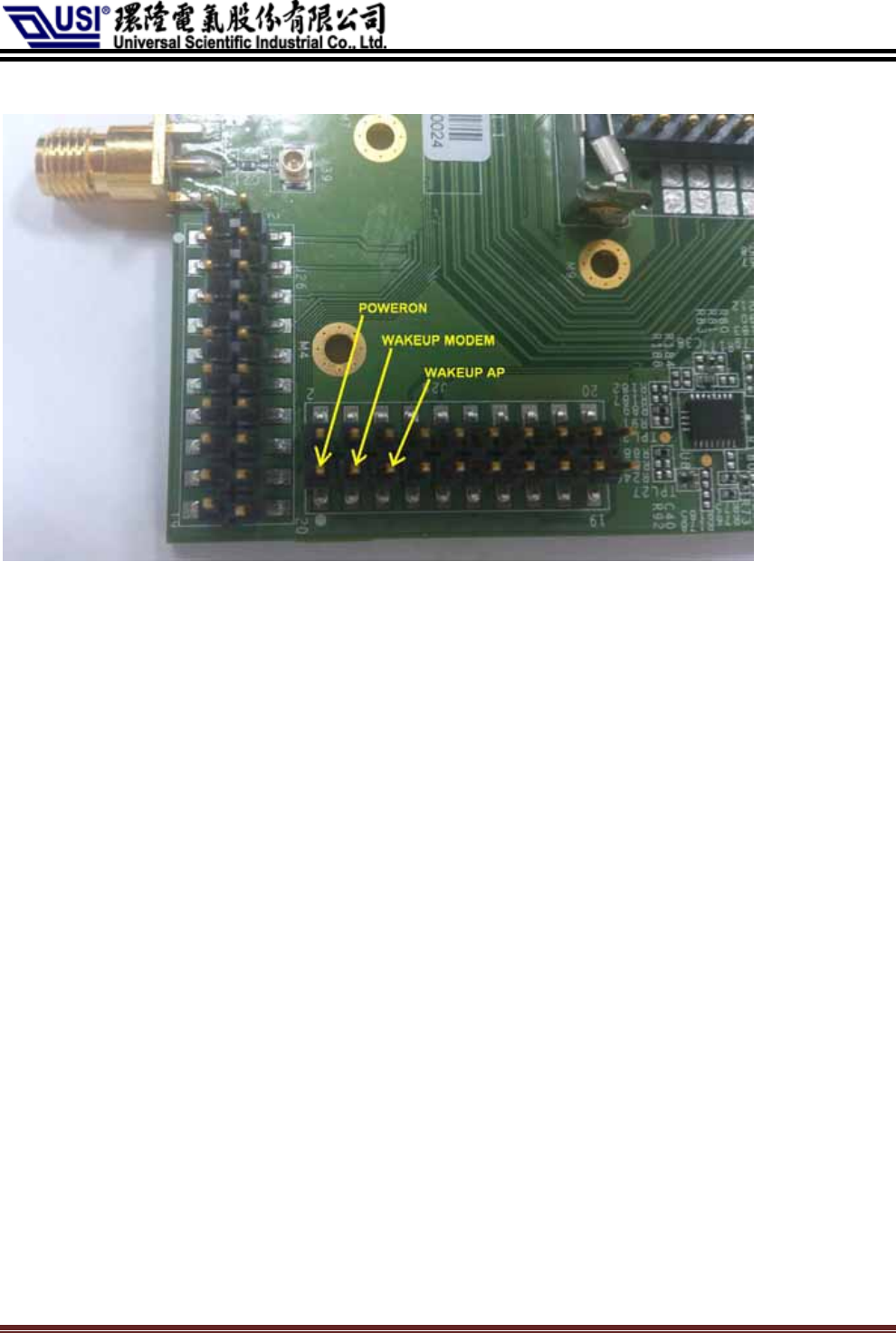
Figure. Positions of POWERON (J25.1), WAKEUP AP (J25.3) and WAKEUP MODEM (J25.5).
The information contained herein is the exclusive property of Universal Scientific Industrial Co., Ltd. and shall not be distributed,
reproduced, or disclosed in whole or in part without prior written permission of USI Co., Ltd. 頁25