VALEO Telematik und Akustik PNADA GSM/GPRS/UMTS/HSDPA/HSUPA Module User Manual V1082 x13 UserManual Rev4
Peiker acustic GmbH & Co. KG GSM/GPRS/UMTS/HSDPA/HSUPA Module V1082 x13 UserManual Rev4
User Manual
_______________________________________________________________________________________________________________
Seite 1
peiker acustic GmbH & Co. KG, Max-Planck-Straße 32, D-61381 Friedrichsdorf, Amtsgericht Bad Homburg HRA 1897
phG: peiker Verwaltungs GmbH, Vorsitzender der Geschäftsführung: Andreas Peiker, Geschäftsführer: Stephan Graf von der Schulenburg, Amtsgericht Bad Homburg 1369
Vorsitzender des Aufsichtsrates: Prof. Dr. Agilolf Lamperstorfer Ein Unternehmen der peiker Firmengruppe
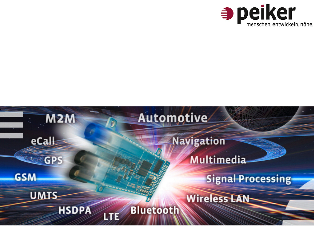
User manual NAD-MDM6200
Peiker product #: 2189-082-112-00 (V1082-x13) HW0811
Revision: 0.4
Date: 10-2011
Status: Approved
_______________________________________________________________________________________________________________
Seite 2
peiker acustic GmbH & Co. KG, Max-Planck-Straße 32, D-61381 Friedrichsdorf, Amtsgericht Bad Homburg HRA 1897
phG: peiker Verwaltungs GmbH, Vorsitzender der Geschäftsführung: Andreas Peiker, Geschäftsführer: Stephan Graf von der Schulenburg, Amtsgericht Bad Homburg 1369
Vorsitzender des Aufsichtsrates: Prof. Dr. Agilolf Lamperstorfer Ein Unternehmen der peiker Firmengruppe
History:
D
ate
Revision
Name
Comment
05.02.1
1
Rev
0.0
ChZi
Initial document
08
-
08
-
2011
Rev 0.1
Gleich /
Herold
Document Review
17
-
08
-
2011
Rev 0.2
Hofmann
Document Review
18
-
08
-
2011
Rev 0.3
Herold /
Hofmann
Document Review; Warning Statement included
06
-
10
-
2011
Rev. 0.4
Herold
IC Canada
Conformance statement
R
eview

_______________________________________________________________________________________________________________
Seite 3
peiker acustic GmbH & Co. KG, Max-Planck-Straße 32, D-61381 Friedrichsdorf, Amtsgericht Bad Homburg HRA 1897
phG: peiker Verwaltungs GmbH, Vorsitzender der Geschäftsführung: Andreas Peiker, Geschäftsführer: Stephan Graf von der Schulenburg, Amtsgericht Bad Homburg 1369
Vorsitzender des Aufsichtsrates: Prof. Dr. Agilolf Lamperstorfer Ein Unternehmen der peiker Firmengruppe
Content
1
Introduction .......................................................................................................................................... 4
1.1 Scope .................................................................................................................................................. 4
1.2 Audience ............................................................................................................................................ 4
1.3 Contact information, Support ......................................................................................................... 4
1.4 Related Documents .......................................................................................................................... 4
2
Overview ............................................................................................................................................... 4
2.1 Product Variants................................................................................................................................ 4
2.3 Features ............................................................................................................................................. 5
2.4 Approvals ........................................................................................................................................... 5
3
Overview ............................................................................................................................................... 6
3.1 Dimension, Mechanical Drawings ................................................................................................... 6
3.2 Block Diagram ................................................................................................................................... 7
3.3 HW Features ...................................................................................................................................... 7
3.4 Connectors ......................................................................................................................................... 8
3.4.1 Base Band Connector ............................................................................................................... 8
3.4.1 Antenna Connectors ................................................................................................................. 8
3.5 Interfaces (40pin Connector).......................................................................................................... 8
3.5.1 USB .............................................................................................................................................. 8
3.5.2 SIM Interface ............................................................................................................................. 8
3.5.3 KPD_POWER .............................................................................................................................. 9
3.5.4 Reset ........................................................................................................................................... 9
3.5.5 Reference Voltage Output (VREG_MSME 1.8V) ................................................................... 9
3.5.6 GPIOs .......................................................................................................................................... 9
3.5.7 GSBIs ........................................................................................................................................... 9
3.5.8 Baseband Connector Pinning ................................................................................................. 11
3.5.7 GPS related Pins ...................................................................................................................... 12
3.5.7 Antenna Diagnostics ............................................................................................................... 12
3.5.7 Antenna Switching .................................................................................................................. 13
3.6 Supply Voltage ................................................................................................................................ 13
3.7 Power Consumption ....................................................................................................................... 14
3.8 Transmitter ...................................................................................................................................... 14
3.9 Receiver ........................................................................................................................................... 14
3.10 Enviromental Specification .......................................................................................................... 14
3.10.1 Temperature Range .............................................................................................................. 14
4
Evaluation Kit ..................................................................................................................................... 16
5
AT Command interface ..................................................................................................................... 18
6
Safety Recommendations ................................................................................................................. 19
7
List of Acronyms ................................................................................................................................ 20
8
Warning Statements ......................................................................................................................... 21

_______________________________________________________________________________________________________________
Seite 4
peiker acustic GmbH & Co. KG, Max-Planck-Straße 32, D-61381 Friedrichsdorf, Amtsgericht Bad Homburg HRA 1897
phG: peiker Verwaltungs GmbH, Vorsitzender der Geschäftsführung: Andreas Peiker, Geschäftsführer: Stephan Graf von der Schulenburg, Amtsgericht Bad Homburg 1369
Vorsitzender des Aufsichtsrates: Prof. Dr. Agilolf Lamperstorfer Ein Unternehmen der peiker Firmengruppe
1 Introduction
1.1 Scope
This document give an overview electrical and functional detail fort he peiker NAD.
1.2 Audience
Informations for integrate the module in other applications.
1.3 Contact information, Support
Peiker
Max-Planck Street 32
D-61381 Friedrichsdorf
http://www.peiker.de
info@peiker.de
1.4 Related Documents
None.
2 Overview
2.1 Product Variants
The NAD-MDM6200 ist available in 3 variants:
Peiker product # WCDMA FDD bands
2189-082-112-00 (V1082-112) HW0811 BC1, BC8 (EU configuration)
2189-082-114-00 (V1082-114) HW0811 BC1 (China configuration)
2189-082-115-00 (V1082-x13) HW0811 BC2, BC5 (US2 configuration)
All variants include Quad band GSM/GPRS/EDGE (850,900,1800,1900)

_______________________________________________________________________________________________________________
Seite 5
peiker acustic GmbH & Co. KG, Max-Planck-Straße 32, D-61381 Friedrichsdorf, Amtsgericht Bad Homburg HRA 1897
phG: peiker Verwaltungs GmbH, Vorsitzender der Geschäftsführung: Andreas Peiker, Geschäftsführer: Stephan Graf von der Schulenburg, Amtsgericht Bad Homburg 1369
Vorsitzender des Aufsichtsrates: Prof. Dr. Agilolf Lamperstorfer Ein Unternehmen der peiker Firmengruppe
2.3 Features
- GSM/GPRS/EDGE Quad band (850, 900, 1800,1900)
- HSUPA up to 5.76 Mbps
- HSDPA up to 14.4 Mbps
- WCDMA up to 384kbps uplink/downlink
- DTM
- eCall inband nodem
Power Classes
- Class 4 (33dBm, 2W) Lo bands 850, 900 GSMK
- Class 1 (30dBm, 1W) Hi bands 1800, 1900 GSMK
- Class E2 Lo bands 850, 900 8PSK (EDGE)
- Class E2 Hi bands 1800, 1900 8PSK (EDGE)
- PS GPRS/EDGE Multi slot class 12 (4Dn/4Up/5Sum max.)
- CS Multi slot class 1 (1Dn/1Up)
- DTM Multi slot class 11 (4Dn/3Up/5Sum max.)
2.4 Approvals
- R&TTE directive
- CE, GCF
- FCC, IC, PTCRB
- AT&T
_______________________________________________________________________________________________________________
Seite 6
peiker acustic GmbH & Co. KG, Max-Planck-Straße 32, D-61381 Friedrichsdorf, Amtsgericht Bad Homburg HRA 1897
phG: peiker Verwaltungs GmbH, Vorsitzender der Geschäftsführung: Andreas Peiker, Geschäftsführer: Stephan Graf von der Schulenburg, Amtsgericht Bad Homburg 1369
Vorsitzender des Aufsichtsrates: Prof. Dr. Agilolf Lamperstorfer Ein Unternehmen der peiker Firmengruppe
3 Overview
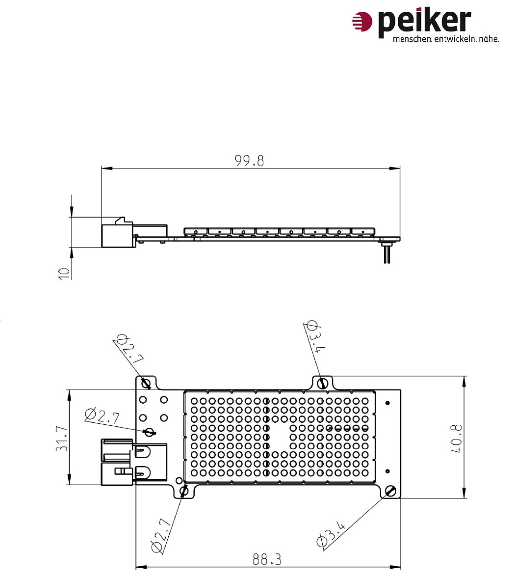
3.1 Dimension, Mechanical Drawings
Figure 1 V1082-x13 Mechanical Dimensions.
Figure 2 V1082-x13 Mechanical Dimensions (Top View).
_______________________________________________________________________________________________________________
Seite 7
peiker acustic GmbH & Co. KG, Max-Planck-Straße 32, D-61381 Friedrichsdorf, Amtsgericht Bad Homburg HRA 1897
phG: peiker Verwaltungs GmbH, Vorsitzender der Geschäftsführung: Andreas Peiker, Geschäftsführer: Stephan Graf von der Schulenburg, Amtsgericht Bad Homburg 1369
Vorsitzender des Aufsichtsrates: Prof. Dr. Agilolf Lamperstorfer Ein Unternehmen der peiker Firmengruppe
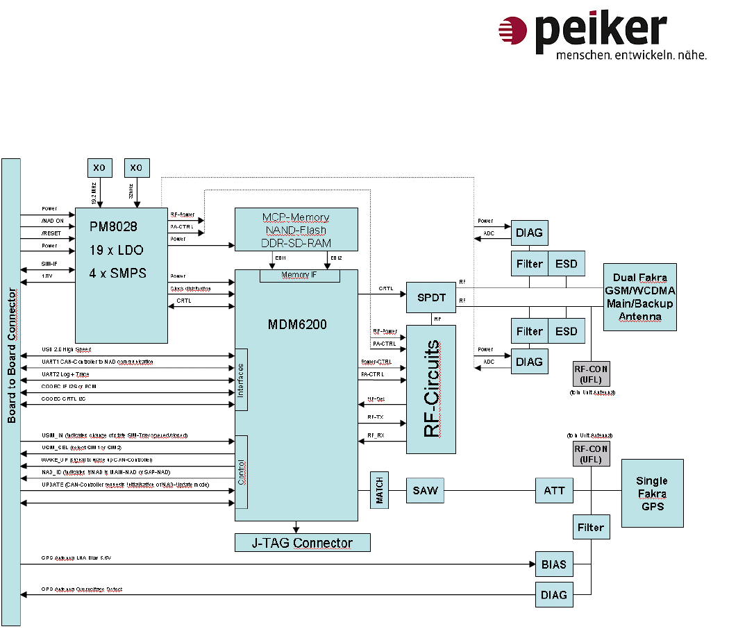
3.2 Block Diagram
Figure 3 V1082-x13 Block Diagram.
3.3 HW Features
- Qualcomm chipset MDM6200 (RF + Base band) + PM8028 (Power management)
- ARM11 Core up to 480 MHz
- 2 DSP for modem and application DSP
- MCP Memory (1Gb NAND Flash x16, 512Mb Mobile DDR SDRAM x16)
- 19.2MHz clock reference
- SPDT switch for main and backup antenna operation
- Onboard antenna diagnostic
- Heavy duty baseband and antenna connector
- Dedicated heat sink area under power amplifier section
- Prepared for GPS/Glonass operation, GPS antenna biasing and diagnostics

_______________________________________________________________________________________________________________
Seite 8
peiker acustic GmbH & Co. KG, Max-Planck-Straße 32, D-61381 Friedrichsdorf, Amtsgericht Bad Homburg HRA 1897
phG: peiker Verwaltungs GmbH, Vorsitzender der Geschäftsführung: Andreas Peiker, Geschäftsführer: Stephan Graf von der Schulenburg, Amtsgericht Bad Homburg 1369
Vorsitzender des Aufsichtsrates: Prof. Dr. Agilolf Lamperstorfer Ein Unternehmen der peiker Firmengruppe
3.4 Connectors
3.4.1 Base Band Connector
The NAD has a 40pin (2x20) connector with 1.27mm pitch. The connector is designed to stitch through
the main board PCB. To allow variable mounting scenarios the 40pin connect can be populated on the
top or the bottom side of NAD PCB. Default location is the PCB bottom side.
3.4.1 Antenna Connectors
To support the usage of a main and backup antenna, the NAD has an automotive dual FAKRA RF-
Connector (SMB male) populated.
The NAD board is prepared for the population of another single FAKRA RF- RF- Connector (SMB male) to
connect a GPS/GLONASS active antenne for simultaneous GPS/GLONASS operation
3.5 Interfaces (40pin Connector)
3.5.1 USB
The NAD has one USB2.0 OTG high speed (480MBit) compliant interface including the phy.
The IF consists of 4 signals:
USB_DP
USB_DM
USB_VBUS
USB_GND
A dynamic reconfiguration between USB-Host or USB-Device is not foreseen, the NAD can be configured
to USB-Host or USB-Device by the insertion of a resistor on the NAD PCB.
3.5.2 SIM Interface
The NADs SIM interface is compatible to 1.8V and 3V SIM Cards, the nessecary voltage and level shifting
is handle by NAD automatically. The IF Consists of the following signals:
VREG_USIM
USIM_CLK
USIM_DATA
USIM_RESET
The data speed on the SIM IF is up to 4 MBit, so HW designers should take care of the length and
routing of the SIM IF to prevent potential EMC problems.

_______________________________________________________________________________________________________________
Seite 9
peiker acustic GmbH & Co. KG, Max-Planck-Straße 32, D-61381 Friedrichsdorf, Amtsgericht Bad Homburg HRA 1897
phG: peiker Verwaltungs GmbH, Vorsitzender der Geschäftsführung: Andreas Peiker, Geschäftsführer: Stephan Graf von der Schulenburg, Amtsgericht Bad Homburg 1369
Vorsitzender des Aufsichtsrates: Prof. Dr. Agilolf Lamperstorfer Ein Unternehmen der peiker Firmengruppe
3.5.3 KPD_POWER
The signal is used switch on the NAD-Module.
KPD_POWER is pulled against VPH_Power on the NAD internally.
Due to this fact it is recommended to pull this input against GND using an open collector or
open drain output only.
3.5.4 Reset
The signal is used to reset the NAD the NAD-Module.
RES_IN is pulled against VPH_Power on the NAD internally.
Due to this fact it is recommended to pull this input against GND using an open collector or
open drain output only.
3.5.5 Reference Voltage Output (VREG_MSME 1.8V)
VREG_MSME is the reference voltage corresponding to the GPIOs/GSBI interfaces of NAD.
VREG_MSME can be used to source interface circuits like level shifters which are connected to
the GPIOs/GSBIs of the NAD. The current on VREG_MSME shall not exceed 30mA.
When using VREG_MSME it is recommended to to decouple the signal with a combination of
1uF and 22pF directly at the baseband connector.
3.5.6 GPIOs
21 GPIOs are available on NAD baseband connector. The reference voltage is of the GPIOs is
1.8V. The GPIOs can be used with flexible input and out configurations, such input with pull up
or pull down, various pull up/down drive strength can be programmed interrupt functionality is
possible. Also output push/pull or output with pull/down can be configured. For details please
refer to latest chipset device specification document 80_VR001-1.
Some the GPIOs are part of the 5 available GSBIs (General Serial Bus Interface).
GPIOs and GSBIs share the same output pins and may not available when used in an GSBI
configuration, see chapter GSBIs.
GPIOs not belonging to a GSBI bundle:
GPIO9,14,17,69,73
GPIOs belonging to a GSBI bundle:
GPIO30,31,32,33,34,35,36,37,38,39,40,41,42,43,46,47
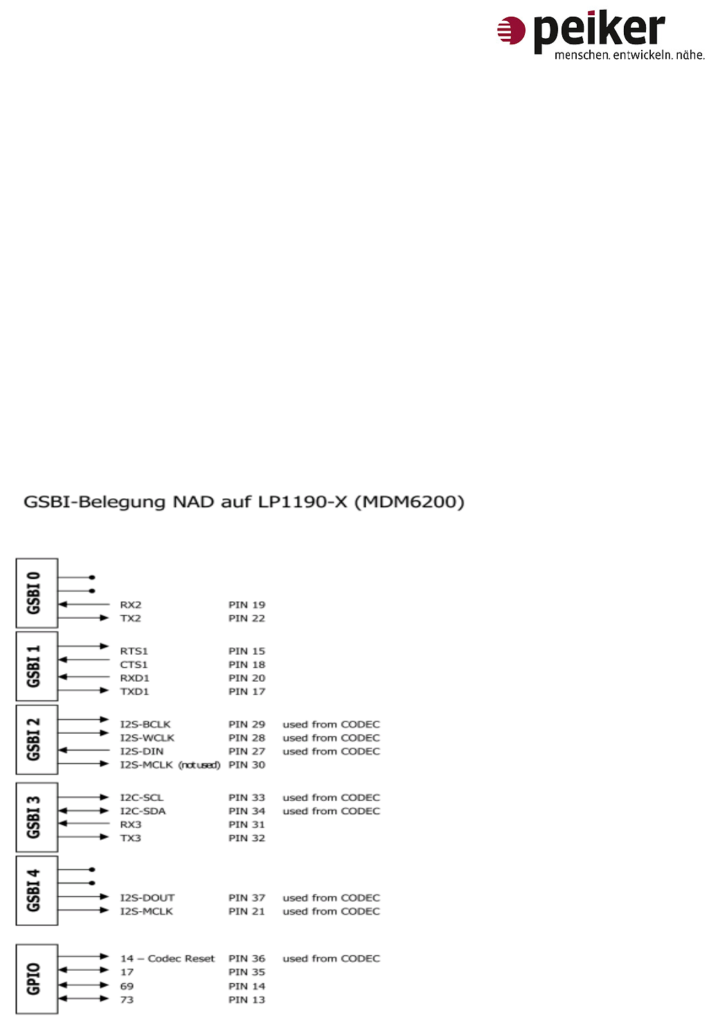
3.5.7 GSBIs
Each GSBI (General Serial Bus Interface) consists of a bundle of 4 GPIOs. 5 GSBI are available.
The reference voltage is of the GSBIs is 1.8V.
Available signals on GSBI bundles:
_______________________________________________________________________________________________________________
Seite 10
peiker acustic GmbH & Co. KG, Max-Planck-Straße 32, D-61381 Friedrichsdorf, Amtsgericht Bad Homburg HRA 1897
phG: peiker Verwaltungs GmbH, Vorsitzender der Geschäftsführung: Andreas Peiker, Geschäftsführer: Stephan Graf von der Schulenburg, Amtsgericht Bad Homburg 1369
Vorsitzender des Aufsichtsrates: Prof. Dr. Agilolf Lamperstorfer Ein Unternehmen der peiker Firmengruppe
GSBI0: GSBI0_2, GSBI0_3 (GPIO_30,31)
GSBI1: GSBI1_0, GSBI1_1, GSBI1_2, GSBI1_3 (GPIO_32,33,34,35)
GSBI2: GSBI2_0, GSBI2_1, GSBI2_2, GSBI2_3 (GPIO_36,37,38,39)
GSBI3: GSBI3_0, GSBI3_1, GSBI3_2, GSBI3_3 (GPIO_40,41,42,43)
GSBI4: GSBI4_2, GSBI4_3 (GPIO_46,47)
Generally the functions of a GSBI are:
UART, UIM, I2C, I2S, SPI, PCM, RTS, CTS, GPIO
For details and possible combinations an GSBIs please refer to latest chipset device
specification document 80_VR001-1.
An example of a possible configuration with I2S audio codec, I2C audio codec control and and 2
UARTS is shown below.
For details also refer to V1102 schematics.

_______________________________________________________________________________________________________________
Seite 11
peiker acustic GmbH & Co. KG, Max-Planck-Straße 32, D-61381 Friedrichsdorf, Amtsgericht Bad Homburg HRA 1897
phG: peiker Verwaltungs GmbH, Vorsitzender der Geschäftsführung: Andreas Peiker, Geschäftsführer: Stephan Graf von der Schulenburg, Amtsgericht Bad Homburg 1369
Vorsitzender des Aufsichtsrates: Prof. Dr. Agilolf Lamperstorfer Ein Unternehmen der peiker Firmengruppe
3.5.8 Baseband Connector Pinning
Pin
Signal
Direction
related to
NAD Parameter Comment
2
GND Input Power Power GND
1
VPH_PWR Input Power 3.8V / 2A peak Main power
4
GND Input Power Power GND
3
VPH_PWR Input Power 3.8V / 2A peak Main power
6
GND Input Power Power GND
5
VPH_PWR Input Power 3.8V / 2A peak Main power
8
VREG_MSME Output Power 1,8V / 30mA Output power to TCB mainboard for sourcing levelshifters
7
KPD_POWER IN / active low
pull down with
o.C. NAD switch on input
10
USIM_CLK OUT 2.85V / 1.8V SIM-Card clock
9
USIM_RST OUT 2.85V / 1.8V SIM-Card reset
12
USIM_DATA I/O 2.85V / 1.8V
SIM-Card data, requires a pull up to VREG_USIM @
destination platform
11
VREG_USIM Output Power
2.85V / 1.8V /
150mA Output power to SIM-Card
14
GPIO_69 I/O 1.8V GPIO
13
GPIO_73 I/O 1.8V GPIO
16
RES_IN IN pull down with o.C
force a reset condition to NAD
15
GPIO_32_GSBI1_0 I/O 1.8V GPIO or GSBI
18
GPIO_33_GSBI1_1 I/O 1.8V GPIO or GSBI
17
GPIO_35_GSBI1_3 I/O 1.8V GPIO or GSBI
20
GPIO_34_GSBI1_2 I/O 1.8V GPIO or GSBI
19
GPIO_30_GSBI0_2 I/O 1.8V GPIO or GSBI
22
GPIO31_GSBI_0_3 I/O 1.8V GPIO or GSBI
21
GPIO_47_ OUT 1.8V GPIO or GSBI
24
USB_VBUS Input Power 5V / 5mA High-Speed USB Device for communication
23
USB_DP IN/OUT USB-Level 3.3V High-Speed USB Device for communication
26
GND_USB Power High-Speed USB Device for communication
25
USB_DM IN/OUT USB-Level 3.3V High-Speed USB Device for communication
28
GPIO_37_GSBI_2_1 I/O 1.8V GPIO or GSBI
27
GPIO_38_GSBI_2_2 I/O 1.8V GPIO or GSBI
30
GPIO_39_GSBI_2_3 I/O 1.8V GPIO or GSBI
29
GPIO_36_GSBI_2_0 I/O 1.8V GPIO or GSBI
32
GPIO_43_GSBI_3_3 I/O 1.8V GPIO or GSBI
31
GPIO_42_GSBI_3_2 I/O 1.8V GPIO or GSBI
34
GPIO_41_GSBI_3_1 I/O 1.8V GPIO or GSBI
33
GPIO_40_GSBI_3_0 I/O 1.8V GPIO or GSBI
36
GPIO_14 I/O 1.8V GPIO
35
GPIO_17 I/O 1.8V GPIO
38
GPIO_9 I/O 1.8V GPIO
37
GPIO_46_GSBI_4_2 I/O 1.8V GPIO or GSBI
40
EXT_5V5 Input Power 5,5V / 100mA Power for inside GPS-Antenna LNA
39
GPS_ANT_OVERVOLT
OUT / active
low Open Collector
Detection of GPS-Antenna short against vehicle battery (8-
18V)

_______________________________________________________________________________________________________________
Seite 12
peiker acustic GmbH & Co. KG, Max-Planck-Straße 32, D-61381 Friedrichsdorf, Amtsgericht Bad Homburg HRA 1897
phG: peiker Verwaltungs GmbH, Vorsitzender der Geschäftsführung: Andreas Peiker, Geschäftsführer: Stephan Graf von der Schulenburg, Amtsgericht Bad Homburg 1369
Vorsitzender des Aufsichtsrates: Prof. Dr. Agilolf Lamperstorfer Ein Unternehmen der peiker Firmengruppe
3.5.7 GPS related Pins
Pin 39 GPS_ANT_OVERVOLTAGE and Pin 40 EXT_5V5 are reserved for future use of the internal
GPS of the NAD.
The pins should be grounded when not used in the design.
3.5.7 Antenna Diagnostics
The NAD is capable to monitor the connection status of both antennas (MAIN and BACKUP)
To monitor the connection status, antennas with internal DC coupled 10k resistors to GND must be used.
The diagnose is performed by NAD SW using 2 ADCs.
The following connection states of the antenna can be monitored:
- Antenna short against GND
- Antenna short against Vbatt (+12V)
- Antenna connected
- Antenna not connected
_______________________________________________________________________________________________________________
Seite 13
peiker acustic GmbH & Co. KG, Max-Planck-Straße 32, D-61381 Friedrichsdorf, Amtsgericht Bad Homburg HRA 1897
phG: peiker Verwaltungs GmbH, Vorsitzender der Geschäftsführung: Andreas Peiker, Geschäftsführer: Stephan Graf von der Schulenburg, Amtsgericht Bad Homburg 1369
Vorsitzender des Aufsichtsrates: Prof. Dr. Agilolf Lamperstorfer Ein Unternehmen der peiker Firmengruppe
3.5.7 Antenna Switching
The NAD is equipped with to antenna connectors. A main and a backup antenna can be connected to the
antenna ports. To switchover between the antennas a SPDT RF- Switch is populated on NAD.
The switch can be performed by SW toggling 2 internal GPIOs on NAD.
At the moment the main antenna is switched on by default. The main antenna is the mapped to the SMB
connector close to the outer dimension of the NAD.
SPDT
Figure 4 V1082-x13 Antenna Connectors.
3.6 Supply Voltage
The external supply voltage is apllied to NAD by 6 Pins on the base band connector.
PINs 1,3,5 for VPH_PWR
PINs 2,4,5 for the corresponding GND
T
A
= -40°C … +85°C
Absolute maximum supply voltage
3.4V ~ 4.2V
Nominal supply voltage
3.8V
Recommended supply voltage
3.7V ~ 3.9V
Voltage drop @ GSM power burst (33dBm)
<100mV
Main Antenna
Backup Antenna
Antenna
Prepared GPS
Antenna connector
Not populated
_______________________________________________________________________________________________________________
Seite 14
peiker acustic GmbH & Co. KG, Max-Planck-Straße 32, D-61381 Friedrichsdorf, Amtsgericht Bad Homburg HRA 1897
phG: peiker Verwaltungs GmbH, Vorsitzender der Geschäftsführung: Andreas Peiker, Geschäftsführer: Stephan Graf von der Schulenburg, Amtsgericht Bad Homburg 1369
Vorsitzender des Aufsichtsrates: Prof. Dr. Agilolf Lamperstorfer Ein Unternehmen der peiker Firmengruppe
During Hi RF Power GSM bursts the power amplifier can draw peak currents > 2Amps at
VPH_PWR. The voltage drop during the GSM burst shall not exceed 100mV (measured at C5 on
the NAD module
3.7 Power Consumption
T
A
= +25°C, VPH_PWR =3.8V
Output Power
Output Power
max. (typ. 23dBm)
0 dBm
Voice call
WCDMA BC1
~530mA
~145mA
Voice call WCDMA BC2
~570mA
~145mA
Voice call WCDMA BC
5
~
630
mA
~
140
mA
Voice call WCDMA BC8
~
580
mA
~
140
mA
PCL 5 (typ. 32.5 dBm)
PCL 19 (typ. 5dBm)
Voice call GSM850
~260mA
~65mA
Voice call GSM900
~270mA
~65mA
PCL 0 (typ.30.5dBm)
PCL 15 (typ.0dBm)
Voice call GSM1800
~165mA
~65mA
Voice call GSM1900
~165mA
~65mA
Standby current GSM
DRX = 5
Tbd mA
Standby current WCDMA
DRX = 7
Tbd mA
3.8 Transmitter
Tbd.
3.9 Receiver
Tbd.
3.10 Enviromental Specification
3.10.1 Temperature Range
Range
Operating temp.
range
-
20°C … +65°C
3GPP spec. conform
Operating temp.
range
-
25°C … +85°C
Note 1
Operational
Performance might slightly
deviate from 3GPP spec.
Storage temp. range
-
40°C … +85°C

_______________________________________________________________________________________________________________
Seite 15
peiker acustic GmbH & Co. KG, Max-Planck-Straße 32, D-61381 Friedrichsdorf, Amtsgericht Bad Homburg HRA 1897
phG: peiker Verwaltungs GmbH, Vorsitzender der Geschäftsführung: Andreas Peiker, Geschäftsführer: Stephan Graf von der Schulenburg, Amtsgericht Bad Homburg 1369
Vorsitzender des Aufsichtsrates: Prof. Dr. Agilolf Lamperstorfer Ein Unternehmen der peiker Firmengruppe
Note 1: Due to temperature specification of the chipset, the temperature of the power manager and the
temperature of the modem chip shall not excced +85°C.

_______________________________________________________________________________________________________________
Seite 16
peiker acustic GmbH & Co. KG, Max-Planck-Straße 32, D-61381 Friedrichsdorf, Amtsgericht Bad Homburg HRA 1897
phG: peiker Verwaltungs GmbH, Vorsitzender der Geschäftsführung: Andreas Peiker, Geschäftsführer: Stephan Graf von der Schulenburg, Amtsgericht Bad Homburg 1369
Vorsitzender des Aufsichtsrates: Prof. Dr. Agilolf Lamperstorfer Ein Unternehmen der peiker Firmengruppe
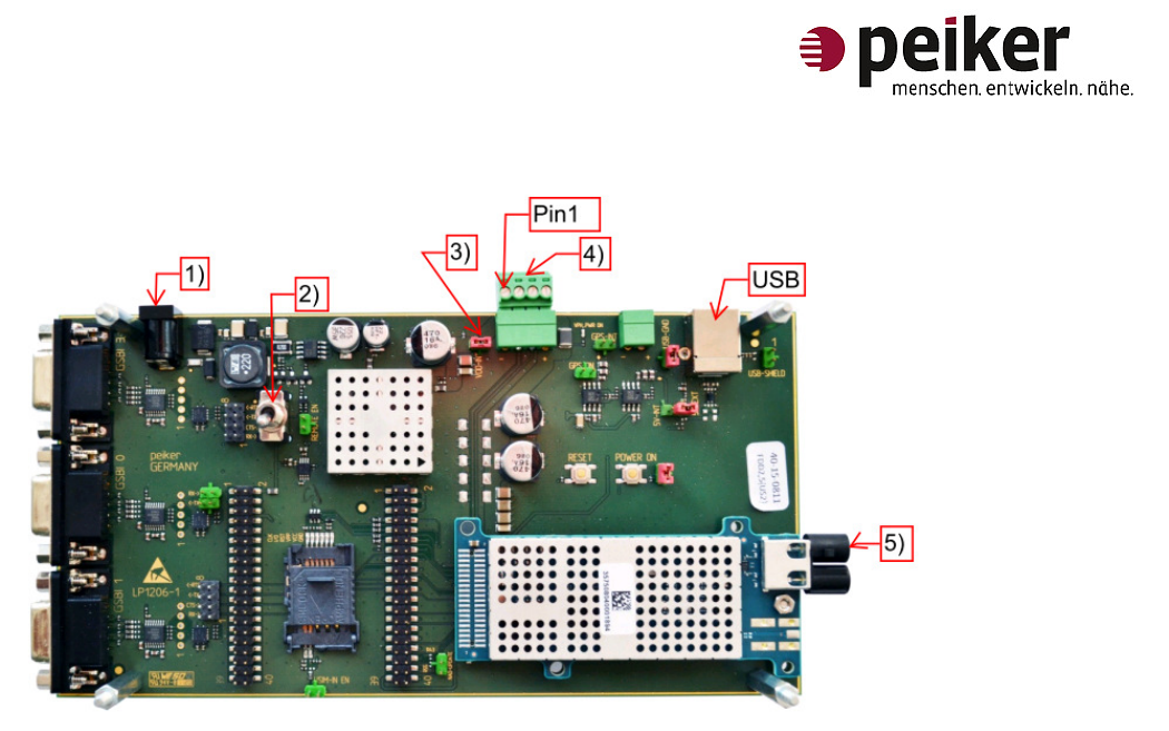
4 Evaluation Kit
For the NAD V1082-x13 there is an evaluation board available.
Features :
- On board 12V DC power supply or 3,8V DC direct connected (i.e. unbuffered).
- USB port type B
- SIM card tray
- 40 pin header connected to the systemconnector of the NAD
- 3 GSPI Port connected to DB9 or pin header. Can be configured as UART od SDIO or SPDIF to
connect audio codecs
Using the evaluation board with on board 3.8V regulator
- Connect 11 .. 14V DC to power connector 1) (use delivered cable)
- Power on the board with switch 2).
Using the evaluation board with an external power supply
- Remove Jumper 3)
- Switch 2) to off condition
- Connect external supply V+ 3.6 .. 4.0V DC to connector 4) (nominal 3.8V DC)
- Connector 4): Pin1: GND
Pin2: Sense GND
Pin3: Sense V+
Pin4: V+
Note: Make sure that the external power supply is not generating spikes or
hazards higher than 4.2V. NAD Module gets damaged when spikes or hazards
above 4.2V are applied
RF Connector
- For RF measurements use main antenna connector 5)
_______________________________________________________________________________________________________________
Seite 17
peiker acustic GmbH & Co. KG, Max-Planck-Straße 32, D-61381 Friedrichsdorf, Amtsgericht Bad Homburg HRA 1897
phG: peiker Verwaltungs GmbH, Vorsitzender der Geschäftsführung: Andreas Peiker, Geschäftsführer: Stephan Graf von der Schulenburg, Amtsgericht Bad Homburg 1369
Vorsitzender des Aufsichtsrates: Prof. Dr. Agilolf Lamperstorfer Ein Unternehmen der peiker Firmengruppe
Figure 5 Evaluation Kit for V1082-x13.
_______________________________________________________________________________________________________________
Seite 18
peiker acustic GmbH & Co. KG, Max-Planck-Straße 32, D-61381 Friedrichsdorf, Amtsgericht Bad Homburg HRA 1897
phG: peiker Verwaltungs GmbH, Vorsitzender der Geschäftsführung: Andreas Peiker, Geschäftsführer: Stephan Graf von der Schulenburg, Amtsgericht Bad Homburg 1369
Vorsitzender des Aufsichtsrates: Prof. Dr. Agilolf Lamperstorfer Ein Unternehmen der peiker Firmengruppe
5 AT Command interface
The modules supports standart AT command as listed below.
Commands are compliant to
3GPP TS 27.007 .
3GPP TS 27.005
Command Description Comment
AT+CMGF Message Format
AT+CSCA Service Centre Address
AT+CMGS Send Message
AT+CGMI Manufacturer Identification
AT+CGMM Request model identification
AT+CGMR Request revision identification
AT+CGSN Request product serial number
AT+CIMI Request international mobile subscriber
identification
AT+CMOD Call mode Only one Parameter is supported by the
device.
AT+CHUP Hang up call
ATD Initiate a CS or PS call or supplementary service
ATA Answer incoming CS call command
ATH Hangup CS call command
AT+CBST Select bearer service type
AT+CEER Extended error report
AT+CVHU Voice hangup control
AT+CREG Network registration
AT+COPS PLMN selection
AT+CLCK Facility lock
AT+CPWD Change password
AT+CLIP Calling line identification presentation
AT+CLIR Calling line identification restriction
AT+CCWA Call waiting
AT+CHLD Call related supplementary services
AT+CUSD Unstructured supplementary service data
AT+CLCC List current calls
AT+CPOL Preferred PLMN list
AT+CPAS Phone active status
AT+CFUN Set phone functionality
AT+CPIN Enter PIN
AT+CSQ Signal quality
AT+CMER Mobile termination event reporting
AT+CSIM Generic SIM access
AT+CRSM Restricted SIM access
AT+CMEE Report mobile termination error
AT+CGDCONT Define PDP context
AT+CGEQREQ Request 3G quality of service profile
AT-CGATT PS attach or detach
AT+CGACT PDP context activate or deactivate
AT+CGPADDR Show PDP address
AT+CGSMS Select service for MO SMS messages
_______________________________________________________________________________________________________________
Seite 19
peiker acustic GmbH & Co. KG, Max-Planck-Straße 32, D-61381 Friedrichsdorf, Amtsgericht Bad Homburg HRA 1897
phG: peiker Verwaltungs GmbH, Vorsitzender der Geschäftsführung: Andreas Peiker, Geschäftsführer: Stephan Graf von der Schulenburg, Amtsgericht Bad Homburg 1369
Vorsitzender des Aufsichtsrates: Prof. Dr. Agilolf Lamperstorfer Ein Unternehmen der peiker Firmengruppe
Command Description Comment
ATE Character Echo ON/OFF
AT+CSMS Check Message Service support
AT+CSMP Set Text Mode Parameters
AT+CSDH Show Text Mode Parameters
AT+CSCB Select Cell Broadcast Message Types
AT+CSAS Save Settings Only one Parameter is supported by the
device.
AT+CRES Restore Settings Only one Parameter is supported by the
device.
AT+CMGL List messages
AT+CNMA New message acknowledgement
AT+CMGC Send Command
AT+CMMS More Messages to Send
AT+ATV DCE response format
AT+ATX Result code selection and call progress
monitoring control
AT+CNMI New Message Indications to TE
AT+CPMS Preferred Message Storage
AT+CMGW Write Message to Memory
AT+CMSS Send Message from Storage
AT+CMGD Delete Messages
AT+CNUM Get MSISDN
AT+CPBS Select phonebook memory storage
AT+CPBR Read phonebook entries
AT+CPBW Writephonebook entry
6 Safety Recommendations
Tbd.

_______________________________________________________________________________________________________________
Seite 20
peiker acustic GmbH & Co. KG, Max-Planck-Straße 32, D-61381 Friedrichsdorf, Amtsgericht Bad Homburg HRA 1897
phG: peiker Verwaltungs GmbH, Vorsitzender der Geschäftsführung: Andreas Peiker, Geschäftsführer: Stephan Graf von der Schulenburg, Amtsgericht Bad Homburg 1369
Vorsitzender des Aufsichtsrates: Prof. Dr. Agilolf Lamperstorfer Ein Unternehmen der peiker Firmengruppe
7 List of Acronyms
3GPP 3 rd Generation Partnership Project
ADC Analog Digital Converter
ADN Abbrieviated Dialing Number
A-GPS Assisted GPS
AMR
Adaptive Multi Rate
AT Attention Command
AWS Advanced Wireless Services
BER Bit Error Rate
CLIP Calling Line Identification Presentation
CLIR Calling Line Identification Restriction
CSD Circuit Switch Data
DARP Downlink Advanced Receiver Performance
DTMF Dual Tone Multi Frequency
FDN Fixed Dialing Number
FTP File Transfer Protocol
GSM Global System for Mobile communication
GPIO General Purpose Input Output
GPRS General Packet Radio Service
GPS Global Positioning Systen
HSPA High Speed Uplink Pachet Access
HW Hardware
LED Led Emitting Diode
MO Mobile Originated
MT Mobile Terminated
OEM Original Equipment Manufacturer
PCB Printed Circuit Board
PCM Pulse Code Modulation
PDU Protocol Data Unit
PIN Personal Identification Number
RF Radio Frequency
RoHs
Restriction of Hazardous Substances
UART
Universal Asynchronous Receiver and Transmitter
USB Universal Serial Bus
USIM
Universal Subscriber Identity Module
UMTS Universal Mobile Telecommunications System
WCDMA
Wideband Code Division Multiple Access

_______________________________________________________________________________________________________________
Seite 21
peiker acustic GmbH & Co. KG, Max-Planck-Straße 32, D-61381 Friedrichsdorf, Amtsgericht Bad Homburg HRA 1897
phG: peiker Verwaltungs GmbH, Vorsitzender der Geschäftsführung: Andreas Peiker, Geschäftsführer: Stephan Graf von der Schulenburg, Amtsgericht Bad Homburg 1369
Vorsitzender des Aufsichtsrates: Prof. Dr. Agilolf Lamperstorfer Ein Unternehmen der peiker Firmengruppe
8 Warning Statements
FCC
NOTE: This equipment has been tested and found to comply with the limits for a Class B digital
device, pursuant to part 15 of the FCC Rules. These limits are designed to provide reasonable
protection against harmful interference in a residential installation. This equipment generates,
uses, and can radiate radio frequency energy and, if not installed and used in accordance with
the instructions, may cause harmful interference to radio communications. However, there is no
guarantee that interference will not occur in a particular installation. If this equipment does
cause harmful interference to radio or television reception, which can be determined by turning
the equipment off and on, the user is encouraged to try to correct the interference by one or
more of the following measures:
- Reorient or relocate the receiving antenna.
- Increase the separation between the equipment and receiver.
- Connect the equipment into an outlet on a circuit different from that to which the
receiver is connected.
- Consult the dealer or an experienced radio/TV technician for help.
(c) The provisions of paragraphs (a) and (b) of this section do not apply to digital devices
exempted from the technical standards under the provisions of § 15.103.
(d) For systems incorporating several digital devices, the statement shown in paragraph (a) or
(b) of this section needs to be contained only in the instruction manual for the main control
unit.
(e) In cases where the manual is provided only in a form other than paper, such as on a
computer disk or over the Internet, the information required by this section may be included in
the manual in that alternative form, provided the user can reasonably be expected to have the
capability to access information in that form.
This device complies with Part 15 of the FCC rules. Operation is subject to the following two
conditions:
(1) this device may not cause harmful interference, and
(2) this device must accept any interference received, including interference that may cause
undesired operation.
IC Canada
This Class b digital apparatus complies with Canadian ICES-003.
Cet appareil numérique de la classe b est conforme à la norme NMB-003 du Canada.

_______________________________________________________________________________________________________________
Seite 22
peiker acustic GmbH & Co. KG, Max-Planck-Straße 32, D-61381 Friedrichsdorf, Amtsgericht Bad Homburg HRA 1897
phG: peiker Verwaltungs GmbH, Vorsitzender der Geschäftsführung: Andreas Peiker, Geschäftsführer: Stephan Graf von der Schulenburg, Amtsgericht Bad Homburg 1369
Vorsitzender des Aufsichtsrates: Prof. Dr. Agilolf Lamperstorfer Ein Unternehmen der peiker Firmengruppe
Le présent appareil est conforme aux CNR d'Industrie Canada applicables aux appareils radio
exempts de licence. L'exploitation est autorisée aux deux conditions suivantes : (1) l'appareil ne
doit pas produire de brouillage, et (2) l'utilisateur de l'appareil doit accepter tout brouillage
radioélectrique subi, même si le brouillage est susceptible d'en compromettre le
fonctionnement.
Modifications
The FCC requires the user to be notified that any changes or modifications made to this device that are not
expressly approved by peiker acustic GmbH & Co. KG could void the user's authority to operate the equipment.