WISOL RPM2470 ZigBee Module User Manual 2 Manual final
WISOL CO., LTD ZigBee Module 2 Manual final
WISOL >
Users Manual

SPECIFICATION
PBA RF Module
Customer -
Model name RP-M2470
Part name WSZGM200C00
Date 2013. 11. 13
REVISION 02
Application Set Top Box
CUSTOMER-CODE -
WISOL CO., LTD.
373-7, Gajang-dong Gyeonggi-do Osan 447-210 Korea
http://www.wisol.co.kr
PBA RF Module WSZGM200C00
ZigBee / 2.4GHz / IEEE802.15.4 15x18x.2.5 mm3, 45pin, 1mm Pitch Version: 02
2 /14 쪽 2013. 11. 11
1. Approval Revision Record
NO REASON RECORD OF REVISION Remarks Revision Page
1 REV00 WSZGM200B00 Approval Releases 2012-03-06 -
2 REV01 FCC ID / IC Number Added
- FCC ID : 2ABA2RPM2470
- IC : 11534A-RPM2470
2013-11-11 -
3 REV02
FCC/IC Notice Added 2013-11-13 -
2. Scope
This specification is applied to ZigBee / IEEE802.15.4
This module has Chip Antenna, 32MHz X-TAL, Single chip MG2470
3. Absolute Maximum Ratings
Symbol Parameter Rating Unit
VDD Chip core supply voltage -0.3 to 2.0 V
3V_IN I/O supply voltage -0.3 to 3.6 V
TSTG Storage Temperature -40 to 85 ℃
PBA RF Module WSZGM200C00
ZigBee / 2.4GHz / IEEE802.15.4 15x18x.2.5 mm3, 45pin, 1mm Pitch Version: 02
3 /14 쪽 2013. 11. 11
4. DC Characteristics
Symbol Parameter Min Typ. Max Unit
3V_IN I/O supply voltage(VDDIO) 2.0 3.0 3.6 V
VIH High level input voltage 2.5 - 3.6 V
VIL Low level input voltage 0 - 0.4 V
VOH High level output voltage 2.5 - 3.6 V
VOL Low level output voltage - - 0.4 V
TA Air temperature -40 - 85
℃
5. Electrical Specification
(Condition: EVM Board, at 25℃, 3V_IN=3.0V)
Parameter Min Typ. Max Unit
Current consumption
MCU active without RX/TX operation,
Peripherals [UART1 & RNG] active - 4.2 - mA
TX Mode
(MCU active and peripherals[UART1 & RNG] active)
@ max (+9.6dBm) output power
@+8dBm output power
@+7dBm output power
@+6dBm output power
@+5dBm output power
@+4dBm output power
@+3dBm output power
@+2dBm output power
@+1dBm output power
@+0dBm output power
-
43
25
- mA
RX Mode
(MCU active and peripherals[UART1 & RNG] active) - 25 - mA
PBA RF Module WSZGM200C00
ZigBee / 2.4GHz / IEEE802.15.4 15x18x.2.5 mm3, 45pin, 1mm Pitch Version: 02
4 /14 쪽 2013. 11. 11
PM1 - 30 - uA
PM2 - 1.25 2 uA
PM3 - 0.1 1 uA
TX / RX and RX / TX turnaround - - 192 us
6. RF Specifications
6-1. RF Characteristics
Parameter Min Typ. Max Unit
RF Characteristics
RF Frequency Range 2405 - 2480 MHz
Maximum Input Level (PER=1%) @250kbps - -1 - dBm
Received RF Bandwidth - 2 - MHz
Channel Bandwidth - 5 - MHz
Receiver Sensitivity
(PER≤1%, Packet length of 22-byte)
@1000kbps
@500kbps
@250kbps
@125kbps
@62.5kbps
@31.25kbps
-
-93
-94
-99
-100
-103
-105
- dBm
Adjacent Channel Rejection
+5MHz
-5MHz
-
30
30
- dB
Alternate Channel Rejection
+10MHz
-10MHz
-
50
50
- dB
Co-Channel Rejection - -5.9 - dB
PBA RF Module WSZGM200C00
ZigBee / 2.4GHz / IEEE802.15.4 15x18x.2.5 mm3, 45pin, 1mm Pitch Version: 02
5 /14 쪽 2013. 11. 11
Blocking / Desensitization
+5MHZ / -5MHz
+10MHZ / -10MHz
+20MHZ / -20MHz
+30MHZ / -30MHz
+50MHZ / -50MHz
-
-53/-52
-48/-46
-44/-40
-43/-38
-41/-37
- dBm
TX output power
* -7dBm±2dB@2480MHz 6 8 9.6 dBm
Transmit chip rate - 2 - Mcps
Spurious Emission(30Hz~1GHz) - -60 - dBm
Spurious Emission(1GHz~12.75GHz) - -45 - dBm
Spurious Emission(5.15GHz~5.3GHz) - -70 - dBm
2nd Harmonics - -45 - dBm
3nd Harmonics - -55 - dBm
Frequency Error Tolerance - - ±200 KHz
Error Vector Magnitude(EVM) - 8.5 - %
Frequency Synthesizer
Phase Noise
(Unmodulated carrier)
@±100KHz offset
@±1MHz offset
@±2MHz offset
@±3MHz offset
@±5MHz offset
-
-79.9
-104.2
-110.0
-113.8
-115.6
- dBc/Hz
PLL Lock Time - - 192 usec
32MHz Crystal Oscillator
Crystal Frequency - 32 - MHz
Crystal Frequency Accuracy Requirement -40 - +40 ppm
Data rate - 250 - kbps
PBA RF Module WSZGM200C00
ZigBee / 2.4GHz / IEEE802.15.4 15x18x.2.5 mm3, 45pin, 1mm Pitch Version: 02
6 /14 쪽 2013. 11. 11
6-2. Analog Temperature
Parameter Min Typ Max Unit
Analog Temperature
Output Voltage at -40℃ - 716 - mV
Output Voltage at 0℃ - 847 - mV
Output Voltage at 40℃ - 978 - mV
Output Voltage at 80℃ - 1109 - mV
Temperature Coefficient - 3.275 - mV/℃
※ All measurement results are obtained using the 12 bit ADC
Analog Temperature
Input Voltage 0 - VDD V
Input Resistance - 150 - kΩ
Full-scale signal - - 3 V
Effective number of bits(ENOB)
Single-ended input, 12bit setting - 10.8 - bits
Effective noise and distortion(SINAD)
Single-ended input, 12bit setting - 66.78 - dB
Current Consumption - 0.62 - mA
Internal Reference Voltage - 1.25 - V
PBA RF Module WSZGM200C00
ZigBee / 2.4GHz / IEEE802.15.4 15x18x.2.5 mm3, 45pin, 1mm Pitch Version: 02
7 /14 쪽 2013. 11. 11
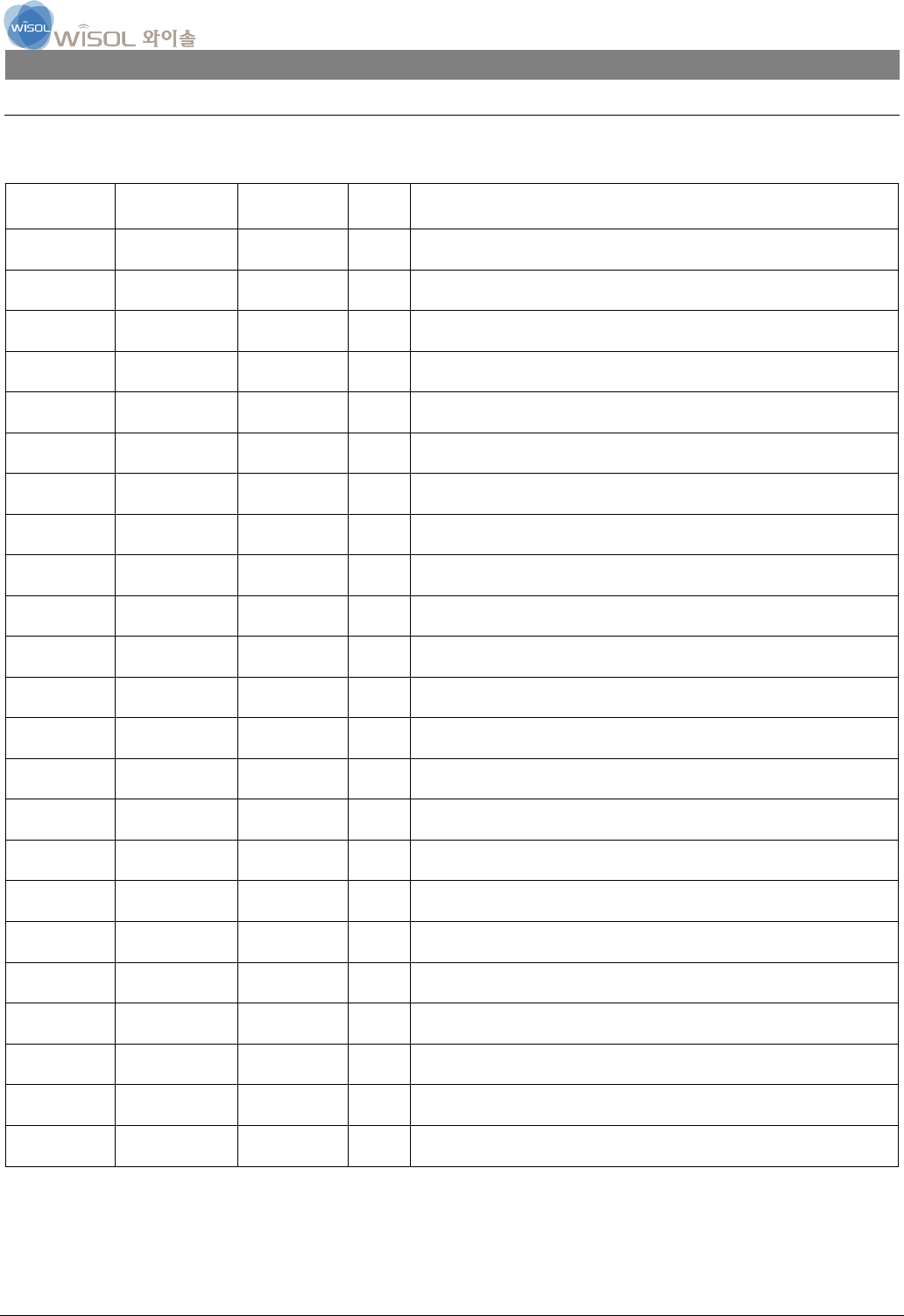
7. Specification on Chip Antenna
PBA RF Module WSZGM200C00
ZigBee / 2.4GHz / IEEE802.15.4 15x18x.2.5 mm3, 45pin, 1mm Pitch Version: 02
8 /14 쪽 2013. 11. 11
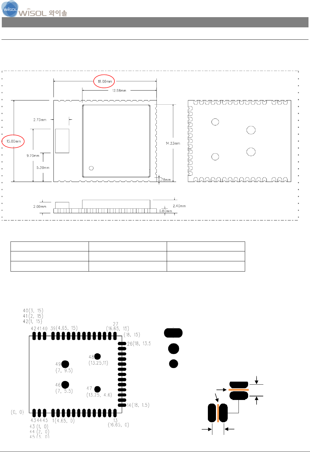
8. Pin Description
Terminal NAME Inter face I/O Description
1 ACH0 Analog I/O Sensor ADC input
2 ACH1 Analog I/O Sensor ADC input
3 ACH2 Analog I/O Sensor ADC input
4 ACH3 Analog I/O Sensor ADC input
5 NC - - -
6 AGND Ground - RF Ground
7 AGND Ground - RF Ground
8 AGND Ground - RF Ground
9 MS2 Digital I Mode select
10 NC - - -
11 RESETB Digital I Reset (Active Low)
12 3V_IN Power I 3V Power supply
13 DGND Ground - Ground for digital core and I/O
14 P1[7] Digital O Port P1.7GPO/P0AND/TRSW/Fold/Clock/BIST Fail Indicator
15 P1[6] Digital B Port P1.6/TRSWB
16 NC - - -
17 P1[4] Digital B Port P1.4 /QUADZB/Sleep Timer OSC Buffer Input.
18 P1[3] Digital B
Port P1.3/QUADZA/Sleep Timer OSC Buffer
Output/RTCLKOUT
19 NC - - -
20 P1[1] Digital B Port P1.1/TXD1
21 P1[0] Digital B Port P1.0/RXD1
22 P3[7] Digital B
Port P3.7/12mA Drive capability
/PWM3/CTS1/SPICSN(slave only)
23 P3[6] Digital B Port P3.6/12 mA Drive capability /PWM2/RTS1/SPICLK
PBA RF Module WSZGM200C00
ZigBee / 2.4GHz / IEEE802.15.4 15x18x.2.5 mm3, 45pin, 1mm Pitch Version: 02
9 /14 쪽 2013. 11. 11
Terminal NAME Inter face I/O Description
24 P3[5] Digital B Port P3.5/T1/CTS0/QUADYB/SPIDO
25 P3[4] Digital B Port P3.4/T0/RTS0/QUADYA/SPIDI
26 P3[3] Digital B Port P3.3/INT1(active low)
27 P3[2] Digital B Port P3.2/INT0(active low)
28 P3[1] Digital B Port P3.1/TXD0/QUADXB
29 P3[0] Digital B Port P3.0/RXD0/QUADXA
30 DGND Ground - Ground for digital core and I/O
31 NC - - -
32 P0[7] Digital B Port P0.7/I2STX_MCLK
33 P0[6] Digital B Port P0.6/I2STX_BCLK
34 P0[5] Digital B Port P0.5/I2STX_LRCK
35 P0[4] Digital B Port P0.4/I2STX_DO
36 P0[3] Digital B Port P0.3/I2SRX_MCLK
37 P0[2] Digital B Port P0.2/I2SRX_BCLK
38 P0[1] Digital B Port P0.1/I2SRX_LRCK
39 P0[0] Digital B Port P0.0/I2SRX_DI
40,41,42 AGND Ground - RF Ground
43,44,45 AGND Ground - RF Ground
46,49 AGND Ground - RF Ground
47,48 DGND Ground - Ground for digital core and I/O
PBA RF Module WSZGM200C00
ZigBee / 2.4GHz / IEEE802.15.4 15x18x.2.5 mm3, 45pin, 1mm Pitch Version: 02
10 /14 쪽 2013. 11. 11
9. Dimensions & drawing
9-1. Design dimension
※ Table A: Real dimension specification
ITEM Width Length
Design 15 mm 18 mm
Real dimension value 14.90mm(*) 17.90mm(*)
(*) : 0.1mm is cut by Dicing blade
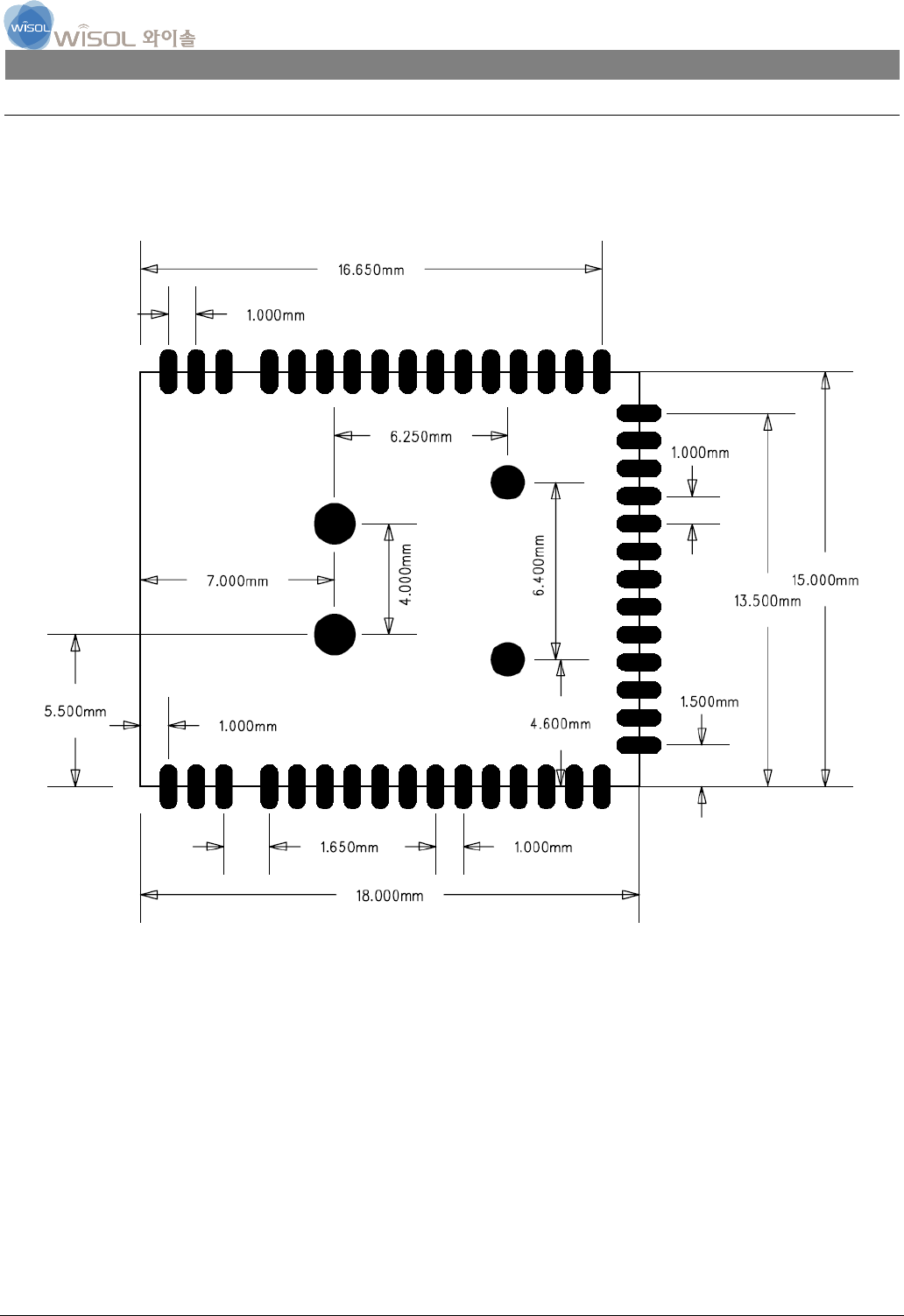
9-2. PCB Drawing -1 (Top View)
Pads of pin 46,49 ; (R=0.75, Circle)
Pads of pin 47,48 ; (R=0.625, Circle)
0.8mm
Pads of pin 1~45 ; (W*L: 0.65*1.6mm)
Silk (w=0.15mm)
Table A
1mm
Weight : 1.04g
PBA RF Module WSZGM200C00
ZigBee / 2.4GHz / IEEE802.15.4 15x18x.2.5 mm3, 45pin, 1mm Pitch Version: 02
11 /14 쪽 2013. 11. 11
9-3. PCB Drawing -2 (Top View)
PBA RF Module WSZGM200C00
ZigBee / 2.4GHz / IEEE802.15.4 15x18x.2.5 mm3, 45pin, 1mm Pitch Version: 02
12 /14 쪽 2013. 11. 11
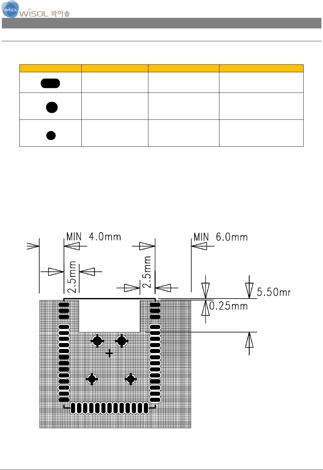
9-4. Solder mask opening guide
9-5. Setup guide for an host devices to install the module
PAD TYPE PAD SIZE MASK open RESULT
W: 0.65mm
L: 1.60mm
W:0.615mm
L:1.76~1.8mm
W: About 95%
L: About 110~115%
R=0.75mm R=0.35mm 46.7%
R=0.625mm R=0.25mm 40%

PBA RF Module WSZGM200C00
ZigBee / 2.4GHz / IEEE802.15.4 15x18x.2.5 mm3, 45pin, 1mm Pitch Version: 02
13 /14 쪽 2013. 11. 11
10. FCC Notice
Federal Communication Commission Interference Statement
This equipment has been tested and found to comply with the limits for a Class B digital device, pursuant to Part 15
of the FCC Rules. These limits are designed to provide reasonable protection against harmful interference in a
residential installation. This equipment generates, uses and can radiate radio frequency energy and, if not installed
and used in accordance with the instructions, may cause harmful interference to radio communications. However,
there is no guarantee that interference will not occur in a particular installation. If this equipment does cause
harmful interference to radio or television reception, which can be determined by turning the equipment off and on,
the user is encouraged to try to correct the interference by one of the following measures:
● Reorient or relocate the receiving antenna.
● Increase the separation between the equipment and receiver.
● Connect the equipment into an outlet on a circuit different from that to which the receiver is connected.
● Consult the dealer or an experienced radio/TV technician for help.
FCC Caution:
Any changes or modifications not expressly approved by the party responsible for compliance could void the user’s
authority to operate this equipment.
This device complies with Part 15 of the FCC Rules. Operation is subject to the following two conditions: (1) This
device may not cause harmful interference, and (2) this device must accept any interference received, including
interference that may cause undesired operation.
FCC Radiation Exposure Statement:
This equipment complies with FCC radiation exposure limits set forth for an uncontrolled environment. This
equipment should be installed and operated with minimum distance 20cm between the radiator & your body. This
device and its antenna(s) must not be co-located or operation in conjunction with any other antenna or transmitter.
USERS MANUAL OF THE END PRODUCT:
In the users manual of the end product, the end user has to be informed to keep at least 20cm separation with the
antenna while this end product is installed and operated. The end user has to be informed that the FCC radio-
frequency exposure guidelines for an uncontrolled environment can be satisfied. The end user has to also be
informed that any changes or modifications not expressly approved by the manufacturer could void the user's
authority to operate this equipment. If the size of the end product is smaller than 8x10cm, then additional FCC part
15.19 statement is required to be available in the users manual: This device complies with Part 15 of FCC rules.
Operation is subject to the following two conditions: (1) this device may not cause harmful interference and (2) this
device must accept any interference received, including interference that may cause undesired operation.
LABEL OF THE END PRODUCT:
The final end product must be labeled in a visible area with the following " Contains FCC ID: 2ABA2RPM2470
". If the size of the end product is larger than 8x10cm, then the following FCC part 15.19 statement has to also be
available on the label: This device complies with Part 15 of FCC rules. Operation is subject to the following two
conditions: (1) this device may not cause harmful interference and (2) this device must accept any interference
received, including interference that may cause undesired operation.

PBA RF Module WSZGM200C00
ZigBee / 2.4GHz / IEEE802.15.4 15x18x.2.5 mm3, 45pin, 1mm Pitch Version: 02
14 /14 쪽 2013. 11. 11
11. IC Notice
IC Statement
This Class B digital apparatus complies with Canadian ICES-003.
Operation is subject to the following two conditions: (1) this device may not cause interference, and (2) this device
must accept any interference, including interference that may cause undesired operation of the device.
Cet appareil numérique de la classe B est conforme á la norme NMB-003 du Canada.
IC Radiation Exposure Statement:
This equipment complies with IC RSS-102 radiation exposure limits set forth for an uncontrolled environment. This
equipment should be installed and operated with minimum distance 20cm between the radiator & your body.
This device and its antenna(s) must not be co-located or operation in conjunction with any other antenna or
transmitter.
IMPORTANT NOTE:
This module is intended for OEM integrator. The OEM integrator is still responsible for the IC compliance
requirement of the end product, which integrates this module.
20cm minimum distance has to be able to be maintained between the antenna and the users for the host this
module is integrated into. Under such configuration, the IC RSS-102 radiation exposure limits set forth for an
population/uncontrolled environment can be satisfied.
Any changes or modifications not expressly approved by the manufacturer could void the user's authority to
operate this equipment.
LABEL OF THE END PRODUCT: The final end product must be labeled in a visible area with the following "
Contains IC : 11534A-RPM2470".