User manual

WiSe 1220 Technical Specification
WiSilica Inc Proprietary and Confidential
WiSe 1220 Hardware and Technical Specification
Preliminary Version (Rev 1.1)
Issued: 21/06/2017
Bluetooth Module

WiSe 1220 Technical Specification
WiSilica Inc Proprietary and Confidential
Table of Contents
General Information ............................................................................................................................... 4
Features .............................................................................................................................................. 4
General Description ............................................................................................................................ 4
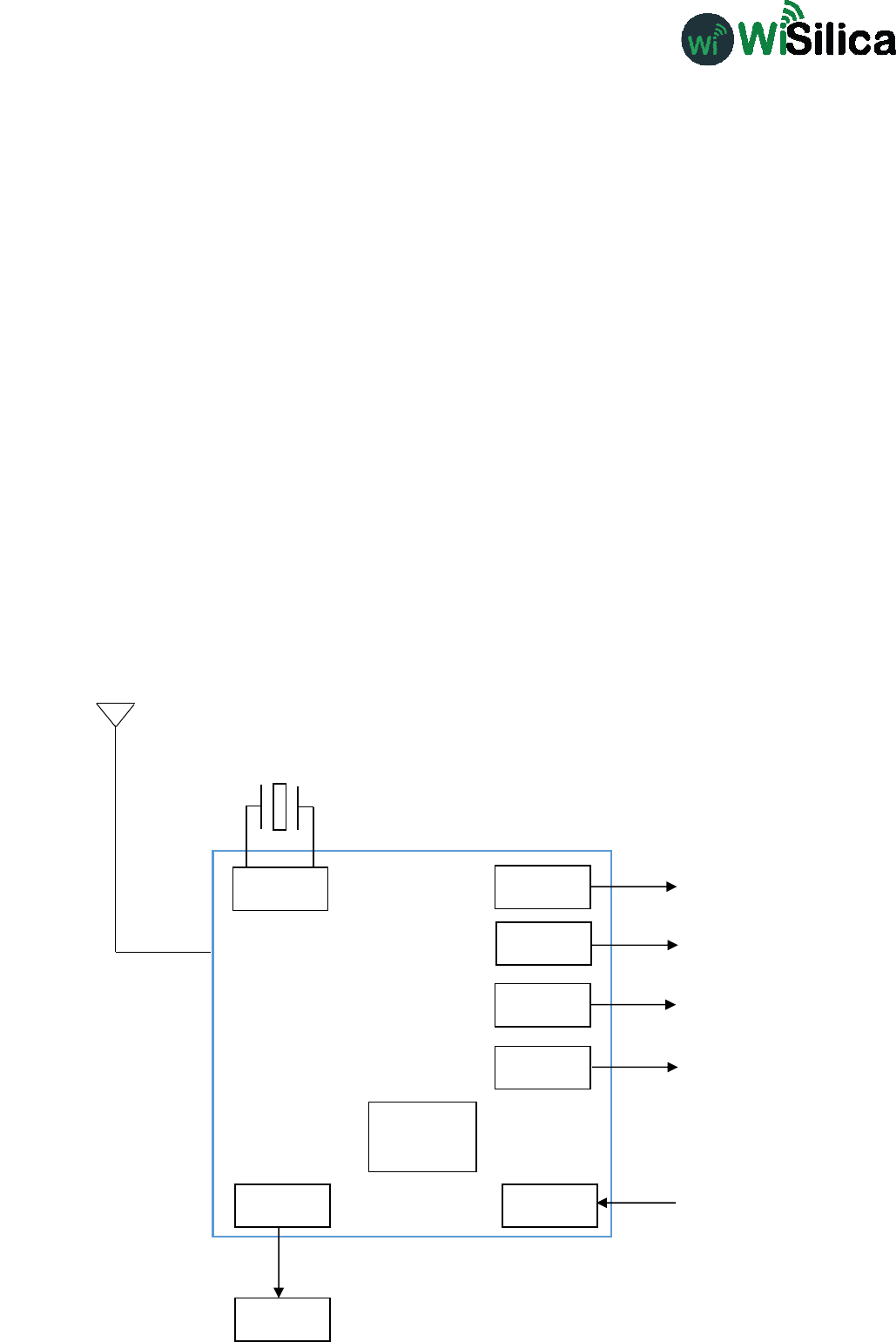
Block Diagram: ........................................................................................................................................ 4
Application: ............................................................................................................................................. 5
Form factor: ............................................................................................................................................ 5
Hardware Specification: .......................................................................................................................... 5
Electrical characteristics.......................................................................................................................... 5
Absolute Maximum Ratings ................................................................................................................ 5
Recommended operating condition ................................................................................................... 6
PWM ....................................................................................................................................................... 6
Current Consumption: ............................................................................................................................ 6
RF Characteristics: ................................................................................................................................... 6
Pinout and Pin Description ..................................................................................................................... 7
Pinout Diagram ................................................................................................................................... 7
Recommended Land Pattern: ................................................................................................................. 9
Host details: ............................................................................................................................................ 9
Remote ................................................................................................................................................ 9
Smart lighting device........................................................................................................................... 9
Best practices .................................................................................................................................... 10

WiSe 1220 Technical Specification
WiSilica Inc Proprietary and Confidential
Revision History
Rev No
Date
Notes
Rev 1.0 07/12/2016
Draft Release
Rev1.1 21/06/2017
Block diagram and host part updated.
WiSe 1220 Technical Specification
WiSilica Inc Proprietary and Confidential
General Information
Features
Bluetooth v4.2 specification complaint
Support for Bluetooth 4.2 specification host stack
12 MHz and 32.768 kHz clock system
32.768 kHz for sleep time
PWM/GPIO/UART interface
PCB printed Antenna
8 programmable GPIO’s
512 KB Internal FLASH
Debug SPI
General Description
WiSe 1220 enables ultra-low-power connectivity and basic data transfer for applications previously
limited by the power consumption, size constraints and complexity of other wireless standards. WiSe
1220 is intended to provide considerably reduced power consumption and cost.
Block Diagram:
BLE CHIP
PWM4
POWER
UART
GPIO
OSC
UART
12MHz
3V
2.4GHz
FLASH
512kb
I2C
SPI

WiSe 1220 Technical Specification
WiSilica Inc Proprietary and Confidential
Application:
WiSe 1220 enables connectivity and data transfer to leading smartphone, tablet and personal
computing devices including Apple iPhone, iPad, iPod and Mac products and leading Android
devices.
Smart mesh light application
Smart home heating and lighting control
Health sensors like blood pressure, thermometer and glucose meter
Beacons
Security
Sensors
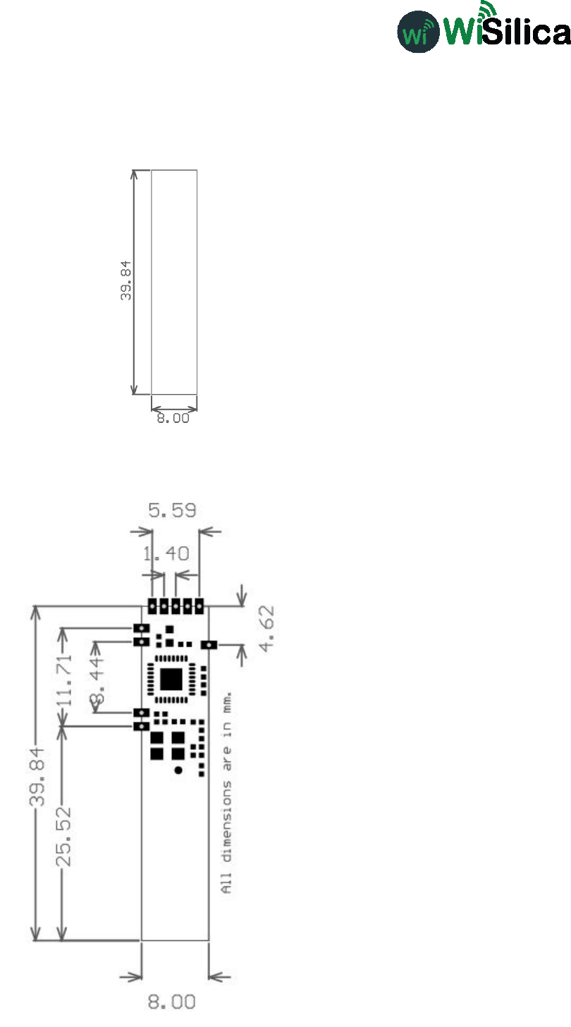
Form factor:
Dimension: 39.84x8mm
Hardware Specification:
COMPON
ENTS
DESCRIPTION
BLE CHIP TLSR8269F512AT32
CRYSTAL 12MHz
Crystal Trim Value and Device ID:
During the manufacturing process, all WiSe1220 Modules are tested for full RF and DC functionality.
This includes measuring crystal frequency error and setting the crystal frequency trim token so the
frequency error for an unmodulated RF tone is as close as possible to zero. At this time a unique
Bluetooth Device Address is assigned to each module.
Electrical characteristics
Absolute Maximum Ratings
Ratings
Min
Ma
x
Storage Temperature
-
40°C
85°C
Supply voltage
2.6
V
3.6
V
IO Supply Voltage
V
3.6V
Other Terminal Voltage
Vss
-
0.4
Vdd + 0.4V

WiSe 1220 Technical Specification
WiSilica Inc Proprietary and Confidential
Recommended operating condition
Item
Min
Typical
Max
Storage Temperature
-
30
-
85°C
Supply voltage
1.9
V
3.3
V
3.6V
IO Sup
ply Voltage
V
-
3.6V
PWM
Totally there are 4 PWM channels. Any of the IO’s can be configured as PWM.
PWM Frequency: Target frequency 40 kHz.
Maximum voltage for logic low: VIL = 0 V
Absolute maximum current sourced: IMAX = mA
Absolute maximum voltage level: VMax = 3.6V
Current Consumption:
Mode
Total Typical Current at 3V
Sleep Mode
6
μA
RX/TX active
~15mA @ 3.3V
peak current
RF Characteristics:
Path
Description
Conditions
Min
Typ
Max
Unit
Operating Frequency
2402
2480
MHz
Maximum output power
7
dBm
2
nd
harmonic
TBD
dBuV
3
rd
harmonic
TBD
dBuV
TX
Modulation de
lta F1 average
TBD
1.3
TBD
M
Hz
Modulation delta F1 / F2
0.8
Modulation delta F2 max
100
%
Frequency accuracy
-
100
25
100
kHz
Frequency offset
-
100
25
100
kHz
RX
Receiver Sensitivity
-
90
-
89
-
86
dBm
Receiver Sensitivity (with dirty tra
nsmitter)
-
92
dBm
Maximum received signal at 30.8% PER
-
10
dBm
WiSe 1220 Technical Specification
WiSilica Inc Proprietary and Confidential
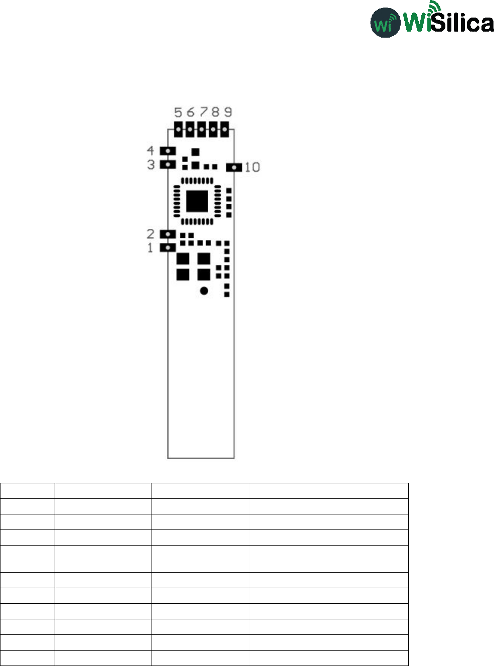
Pinout and Pin Description
Pinout Diagram
PINS NAME FUNCTION COMMENTS
1 RX UART Programmable I/O or RX
2 TX UART Programmable I/O or TX
3 GND Ground Ground
4 SWS/PWM2
PWM/
Programming pins Single Wire Interface
5 PWM5 PWM/IO Programmable I/O
6 PWM4_N PWM/IO Programmable I/O
7 PWM4 PWM/IO Programmable I/O
8 PWM0 PWM/IO Programmable I/O
9 PWM1 PWM/IO Programmable I/O
10 VDD Power 3V3 Input
WiSe 1220 Technical Specification
WiSilica Inc Proprietary and Confidential
Module Dimension
WiSe 1220 Technical Specification
WiSilica Inc Proprietary and Confidential
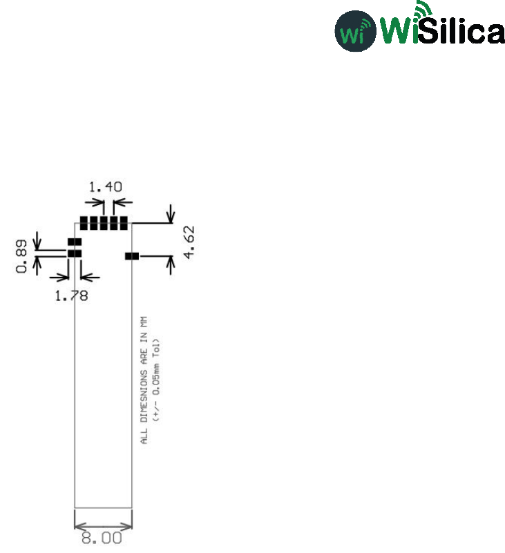
Recommended Land Pattern:
Host details:
The WiSe1220 module is going to be embedded with different products like Remote and Smart
lighting device.
Remote
Remote is used to send the trigger command to the heater or the device associated with that.
It is intended to be a general purpose remote control. Also this device is the 2 x AA battery
powered.
Smart lighting device
The smart lighting device not only controls lighting, it creates a smart mesh which also can be
used to track personnel, assets, patients, anything that is equipped with or wearing a WiSilica
BLE Tag. There is a tremendous amount of possibilities when you think about security, Workflow
management, inventory management, and whole building automation. Also this device is 110 to
230V AC powered.

WiSe 1220 Technical Specification
WiSilica Inc Proprietary and Confidential
Best practices
When designing with WiSe1220 modules, please pay attention to the following recommendations
•While integrating module make sure all the module pads are soldered properly.
•The module's voltage requirement is 2.5 to 3.6V, if the power supply is over 3.3V, please
use a voltage regulator.
•If the communicating host uses a different voltage then the BLE module, please make
sure that the voltage matches on the communication ports.
•For best wireless signals, please avoid packing the antenna area close to metal parts or
case.

WiSe 1220 Technical Specification
WiSilica Inc Proprietary and Confidential
FCC Statement
This device complies with part 15 of the FCC rules. Operation is subject to the following two cond
itions: (1) this device may not cause harmful interference, and (2) this device must accept any int
erference received, including interference that may cause undesired operation.
Changes or modifications not expressly approved by the party responsible for compliance could v
oid the user’s authority to operate the equipment.
NOTE: This equipment has been tested and found to comply with the limits for a Class B digital de
vice, pursuant to part 15 of the FCC Rules. These limits are designed to provide reasonable protec
tion against harmful interference in a residential installation. This equipment generates uses and
can radiate radio frequency energy and, if not installed and used in accordance with the instructi
ons, may cause harmful interference to radio communications. However, there is no guarantee th
at interference will not occur in a particular installation. If this equipment does cause harmful int
erference to radio or television reception, which can be determined by turning the equipment off
and on, the user is encouraged to try to correct the interference by one or more of the following
measures:
‐ Reorient or relocate the receiving antenna.
‐ Reorient or relocate the receiving antenna.
‐ Reorient or relocate the receiving antenna.
‐Consult the dealer or an experienced radio/TV technician for help important announcement
Important Note:
Radiation Exposure Statement
This equipment complies with FCC radiation exposure limits set forth for an uncontrolled
environment.
Important Note:
In the event that these conditions cannot be met (for example certain laptop configurations or
co-location with another transmitter), then the FCC authorization is no longer considered valid
and the FCC ID cannot be used on the final product. In these circumstances, the OEM integrator
will be responsible for re-evaluating the end product (including the transmitter) and obtaining a
separate FCC authorization.
End Product Labeling
The final end product must be labeled in a visible area with the following" Contains FCC ID: 2AG4
NWISE1220 ".
Manual Information to the End User
The OEM integrator has to be aware not to provide information to the end user regarding how to
install or remove this RF module in the user’s manual of the end product which integrates this
module. The end user manual shall include all required regulatory information/warning as show
in this manual.