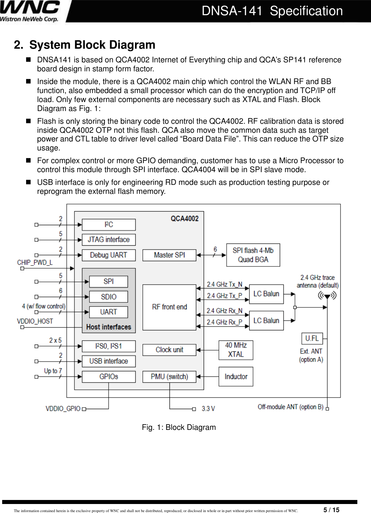
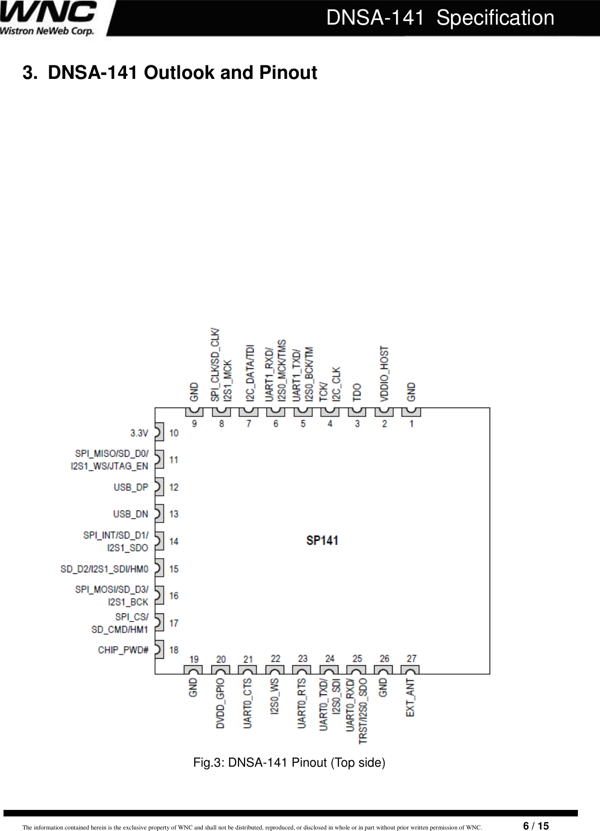
Wistron NeWeb DNSA141 802.11n 1x1 IoE module User Manual MODEL SPECIFICATIONS
Wistron NeWeb Corporation 802.11n 1x1 IoE module MODEL SPECIFICATIONS
UserManual.wiki
>
Wistron NeWeb
>
DNSA141 User Manual
User Manual.pdf
Navigation menu
Upload a User Manual
Namespaces
Wiki Guide
HTML
PDF
Info
Views
User Manual
Discussion / Help
Navigation
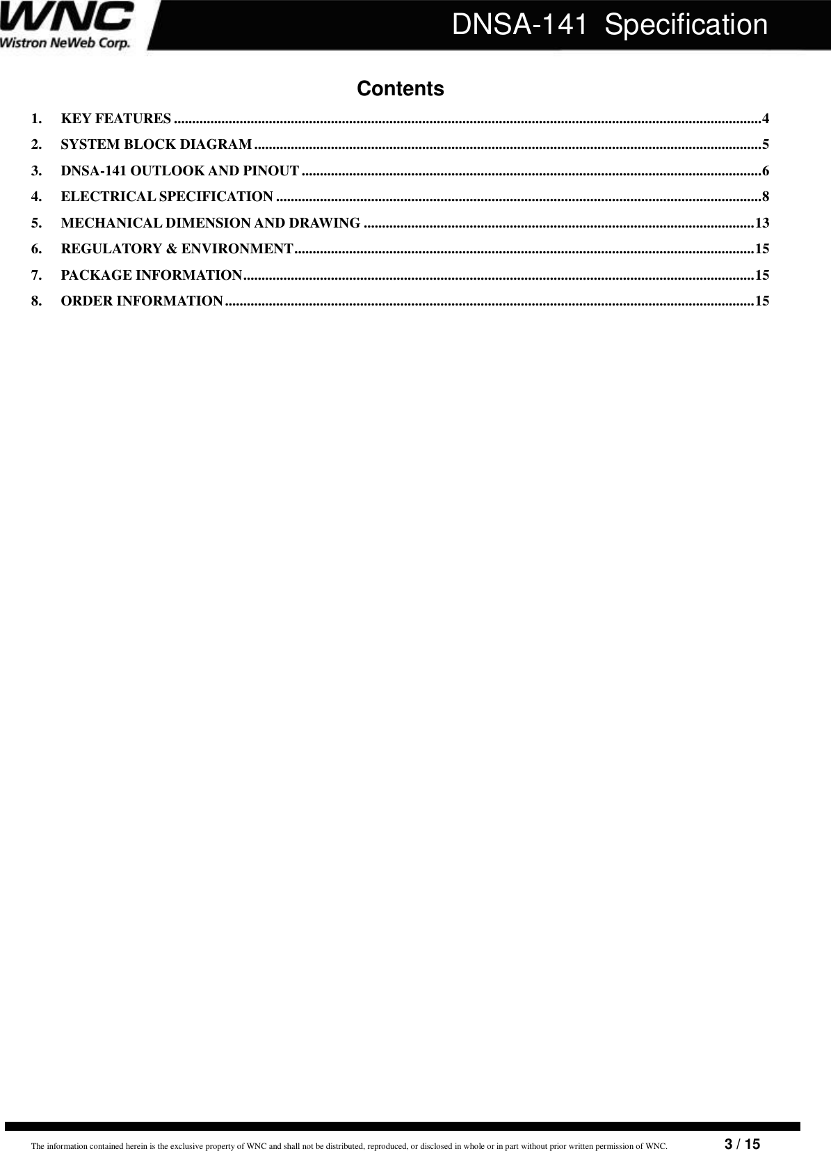
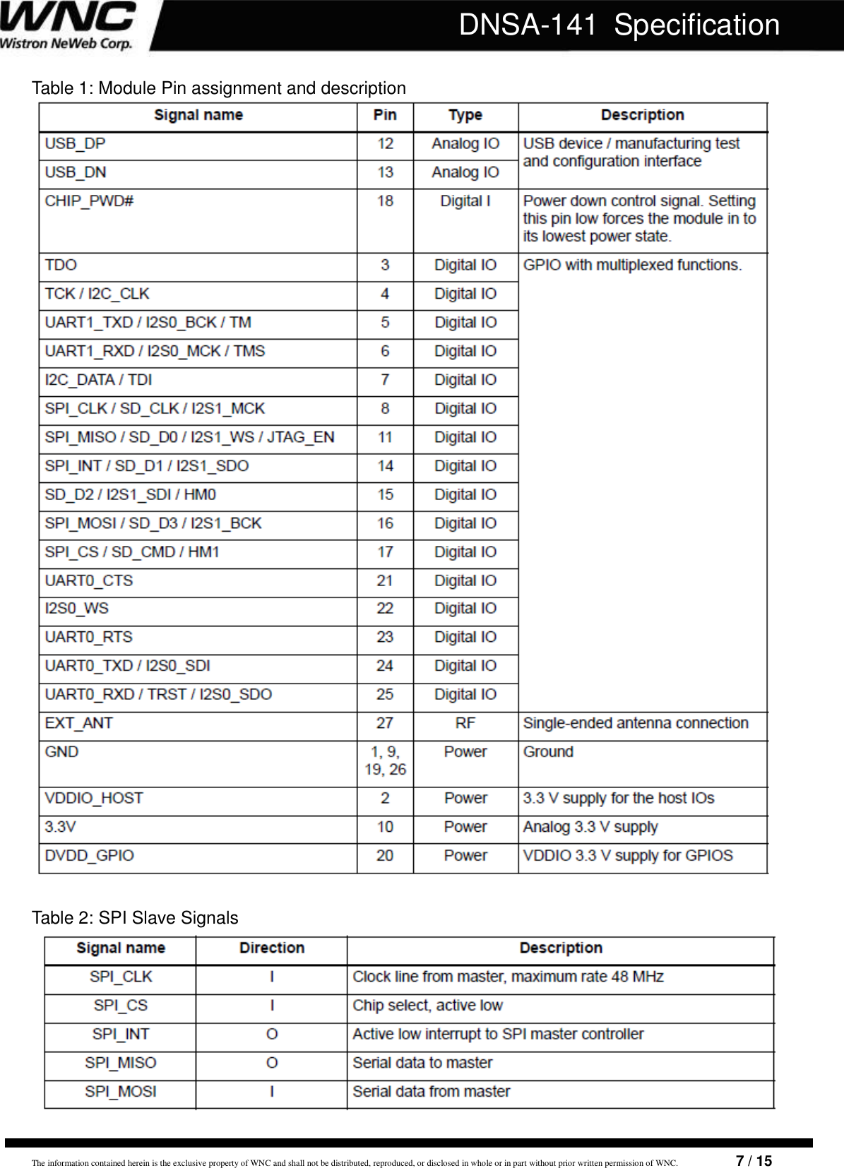
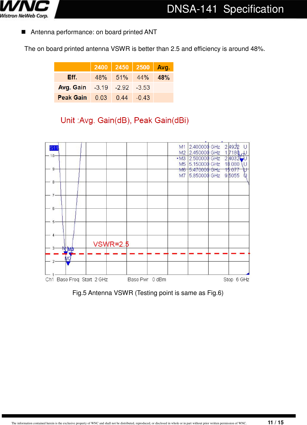
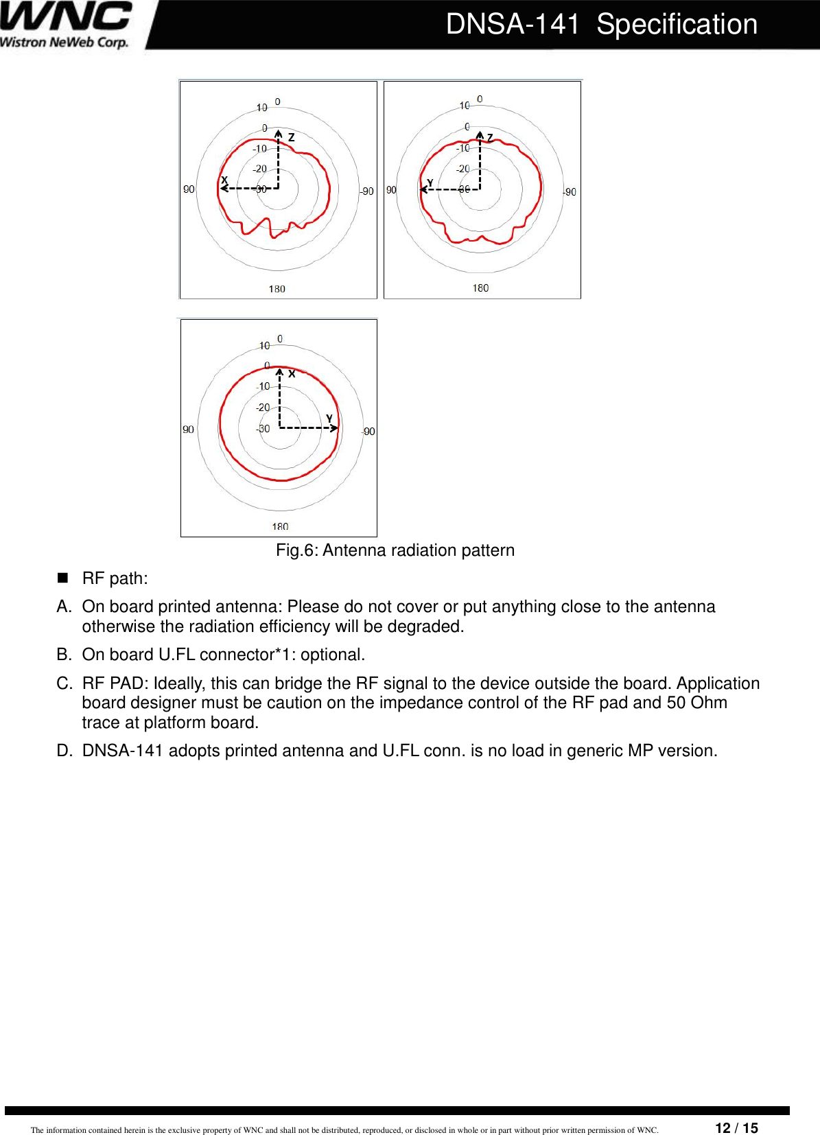
![The information contained herein is the exclusive property of WNC and shall not be distributed, reproduced, or disclosed in whole or in part without prior written permission of WNC. 10 / 15 DNSA-141 Specification RF Tx target power [unit:dBm], IEEE mask and EVM compliance power. Mode/Rate MHz 2412~2472 11b 1Mbps 17 11b 11Mbps 17 11g 6Mbps 18 11g 54Mbps 14 11n HT20 MCS0 18 11n HT20 MCS7 13 11n HT40 MCS0 16 11n HT40 MCS7 12 RF Rx sensitivity [unit:dBm]: Mode/Rate MHz 2412~2472 11b 1Mbps -92 11b 11Mbps -85 11g 6Mbps -88 11g 54Mbps -71 11n HT20 MCS0 -87 11n HT20 MCS7 -67 11n HT40 MCS7 -64](https://usermanual.wiki/Wistron-NeWeb/DNSA141/User-Guide-2356444-Page-10.png)