Wistron NeWeb DNSA141 802.11n 1x1 IoE module User Manual MODEL SPECIFICATIONS
Wistron NeWeb Corporation 802.11n 1x1 IoE module MODEL SPECIFICATIONS
User Manual.pdf
The information contained herein is the exclusive property of WNC and shall not be distributed, reproduced, or disclosed in whole or in part without prior written permission of WNC. 1 / 15
DNSA-141 Specification
Version 0.6
May 15, 2014
Networking Business Unit
Wistron Neweb Corporation
CONFIDENTIAL
THIS DOCUMENT CONTAINS PROPRIETARY TECHNICAL INFORMATION, WHICH IS THE PROPERTY OF THE
WISTRON NEWEB CORPORATION AND SHALL NOT BE DISCLOSED TO OTHERS IN WHOLE OR IN PART,
REPRODUCED, COPIED, OR USED AS THE BASIS FOR DESIGN, MANUFACTURING, OR SALE OF
APPARATUS WITHOUT WRITTEN PERMISSION OF WISTRON NEWEB CORPORATION.
Product Specification for model
DNSA-141
Stamp Type IoE Module
The information contained herein is the exclusive property of WNC and shall not be distributed, reproduced, or disclosed in whole or in part without prior written permission of WNC. 2 / 15
DNSA-141 Specification
Revision History
Rev.
History
Date
Author
V0.4
- Initial version
2014/1/22
TT
V0.5
- Update RF Tx power and Rx Sensitivity, Antenna pattern based on real module
2014/2/21
TT
V0.6
- Update the absolute rating and recommend use SPI for customer application, AT
comments and package
2014/5/15
TT
-
-

The information contained herein is the exclusive property of WNC and shall not be distributed, reproduced, or disclosed in whole or in part without prior written permission of WNC. 3 / 15
DNSA-141 Specification
Contents
1. KEY FEATURES ................................................................................................................................................................. 4
2. SYSTEM BLOCK DIAGRAM ........................................................................................................................................... 5
3. DNSA-141 OUTLOOK AND PINOUT .............................................................................................................................. 6
4. ELECTRICAL SPECIFICATION ..................................................................................................................................... 8
5. MECHANICAL DIMENSION AND DRAWING ........................................................................................................... 13
6. REGULATORY & ENVIRONMENT .............................................................................................................................. 15
7. PACKAGE INFORMATION ............................................................................................................................................ 15
8. ORDER INFORMATION ................................................................................................................................................. 15

The information contained herein is the exclusive property of WNC and shall not be distributed, reproduced, or disclosed in whole or in part without prior written permission of WNC. 4 / 15
DNSA-141 Specification
1. Key Features
QCA4002 IoE solution
Internal PA and LNA, no external RF switch
2.4GHz Single band IEEE 802.11b/g/n, single stream 1x1
11n support HT20 and HT40 Bandwidth
On board printed antenna and U.FL antenna connector(optional)
GPIO voltage is flexible, can between 1.8~3.3V
Single power supply: 3.3V, Low Power Consumption, also support Green Tx and very low
power sleep mode for mobile battery operation application. Can be wake up and go to sleep
quickly.
25mm x 20mm size, 2-layer, single side component
Operation temperature: -40~+85 degrees C(Industry Class Version)
TCP/IP offload, include Encryption
SPI Slave interface to the MCU.
Pre-certified FCC
The information contained herein is the exclusive property of WNC and shall not be distributed, reproduced, or disclosed in whole or in part without prior written permission of WNC. 5 / 15
DNSA-141 Specification
2. System Block Diagram
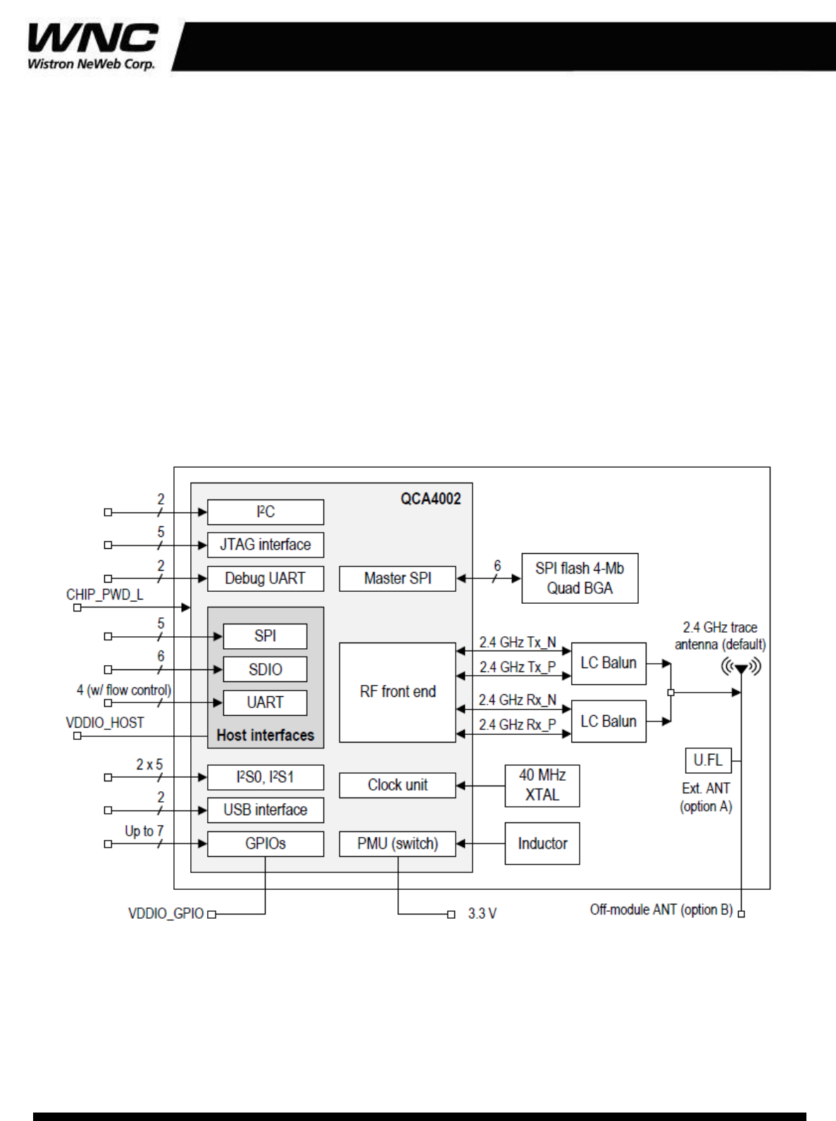
DNSA141 is based on QCA4002 Internet of Everything chip and QCA’s SP141 reference
board design in stamp form factor.
Inside the module, there is a QCA4002 main chip which control the WLAN RF and BB
function, also embedded a small processor which can do the encryption and TCP/IP off
load. Only few external components are necessary such as XTAL and Flash. Block
Diagram as Fig. 1:
Flash is only storing the binary code to control the QCA4002. RF calibration data is stored
inside QCA4002 OTP not this flash. QCA also move the common data such as target
power and CTL table to driver level called “Board Data File”. This can reduce the OTP size
usage.
For complex control or more GPIO demanding, customer has to use a Micro Processor to
control this module through SPI interface. QCA4004 will be in SPI slave mode.
USB interface is only for engineering RD mode such as production testing purpose or
reprogram the external flash memory.
Fig. 1: Block Diagram
The information contained herein is the exclusive property of WNC and shall not be distributed, reproduced, or disclosed in whole or in part without prior written permission of WNC. 6 / 15
DNSA-141 Specification
3. DNSA-141 Outlook and Pinout
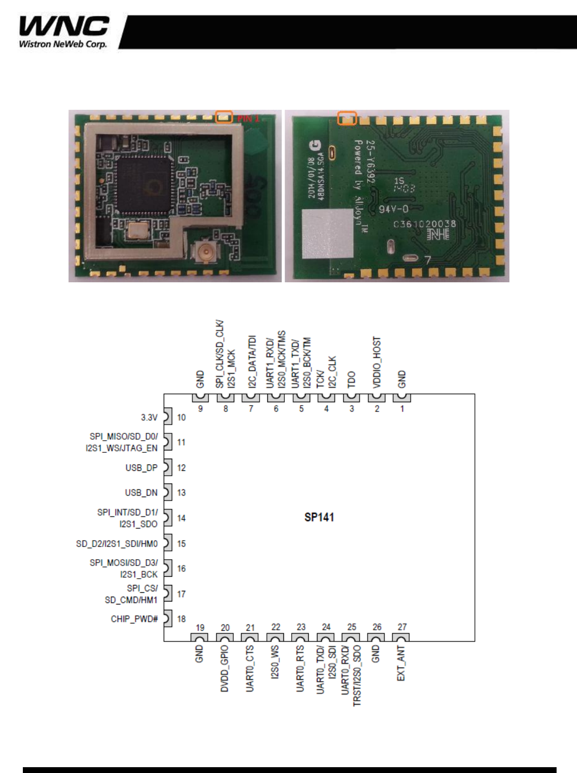
Fig.2: DNSA-141 Outlook (Left: Top side, Right: Bottom side)
Fig.3: DNSA-141 Pinout (Top side)
The information contained herein is the exclusive property of WNC and shall not be distributed, reproduced, or disclosed in whole or in part without prior written permission of WNC. 7 / 15
DNSA-141 Specification
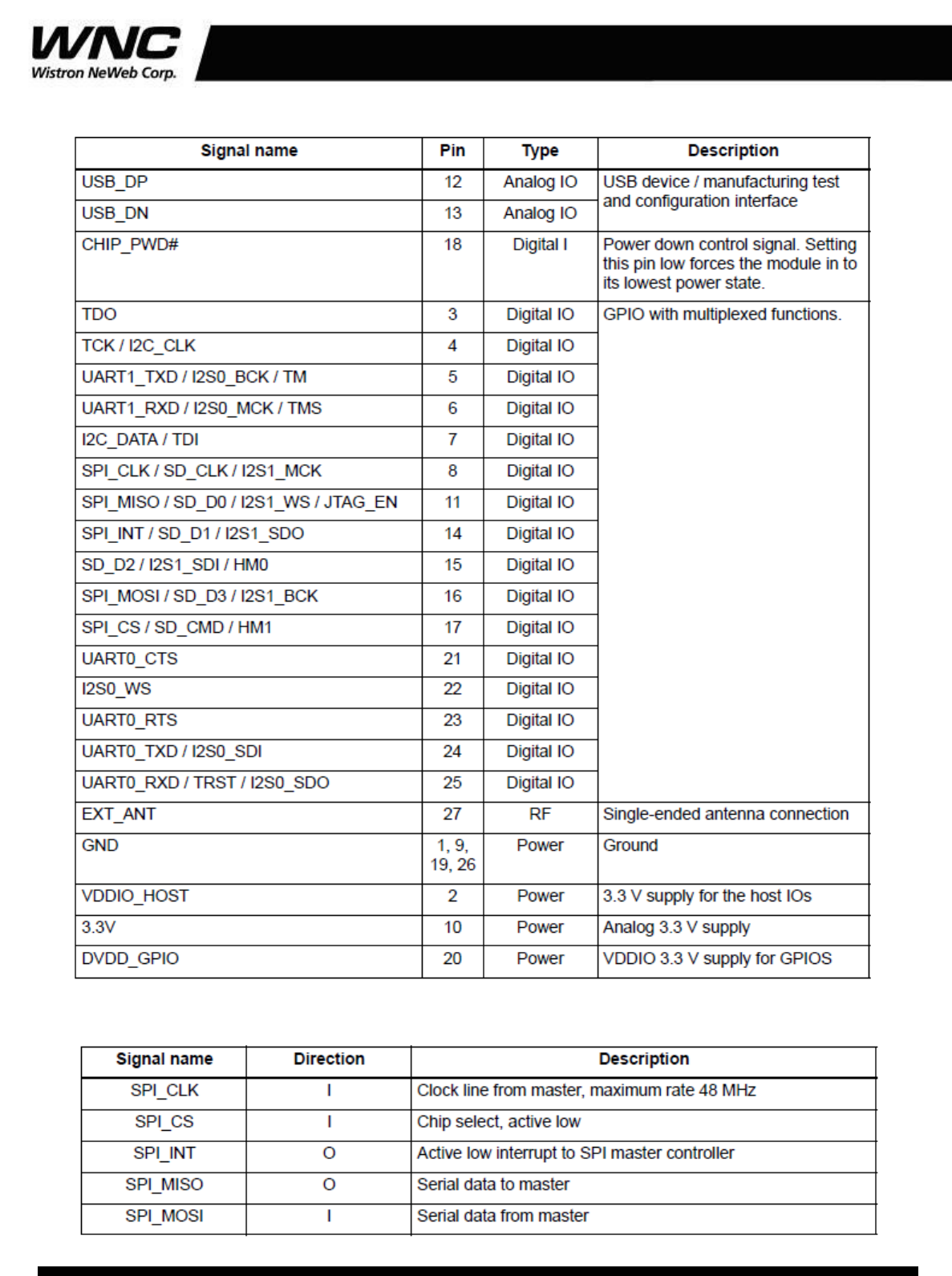
Table 1: Module Pin assignment and description
Table 2: SPI Slave Signals
The information contained herein is the exclusive property of WNC and shall not be distributed, reproduced, or disclosed in whole or in part without prior written permission of WNC. 8 / 15
DNSA-141 Specification
4. Electrical Specification
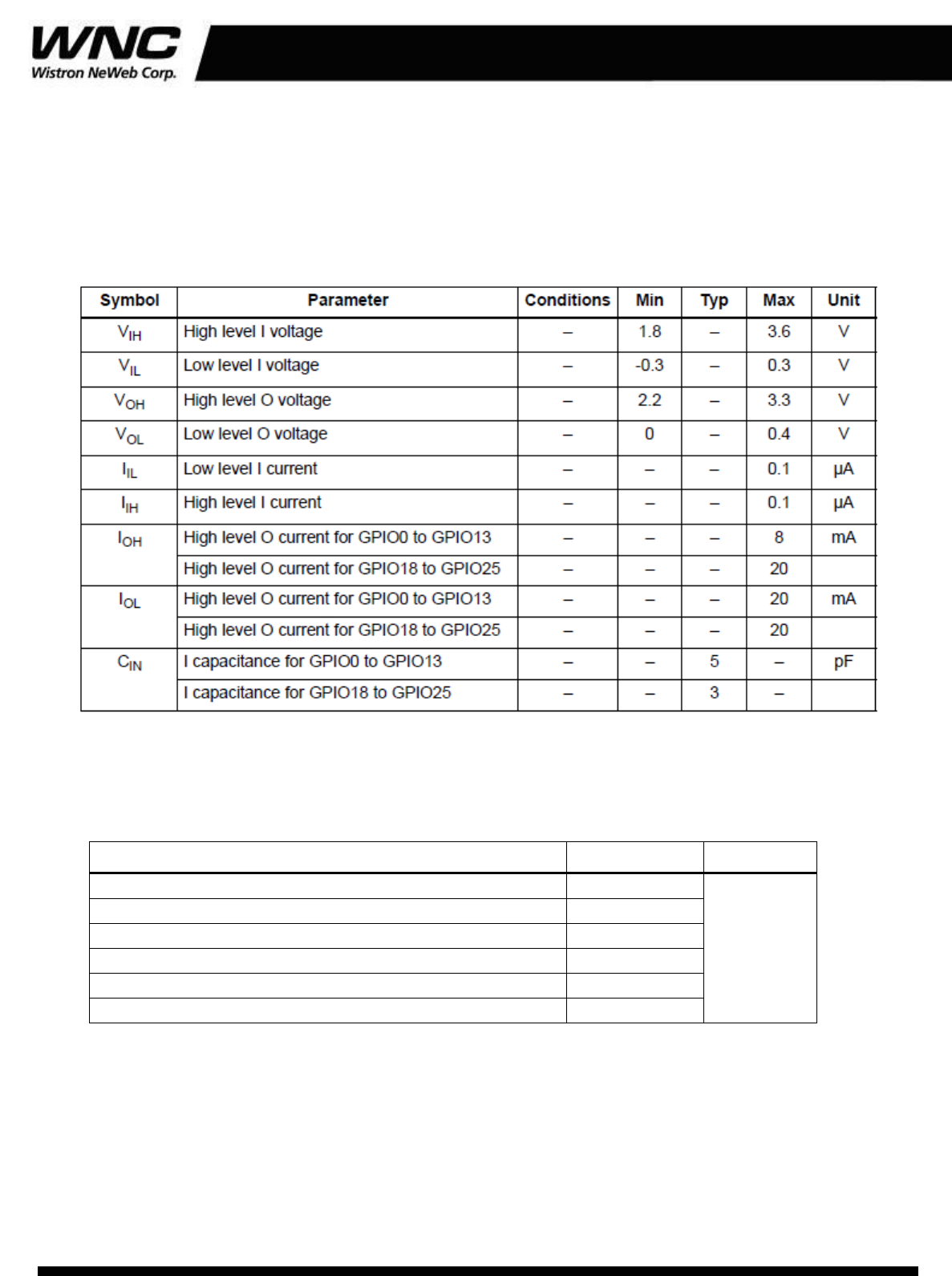
General DC electrical characteristics
These conditions apply to all DC characteristics unless otherwise specified:
Temp = 25 °C, VDD33= 3.3 V
Table 3: DC electrical characteristics for digital I/Os
Power Consumption
Vcc=3.3V, Room temperature
Condition
Average
Unit
11g continue Tx@6M_18dBm
810
mWatt
11n continue Tx@HT40MCS7_12dBm
600
11b/g and 11n HT20 continue Rx
210
11n HT40 continue Rx
240
Chip Power Down
0.04
Sleep
0.4
Note A: External IO voltage (DVDD_GPIO) can be 1.8~3.4V.
Note B:QCA4002 need 3.3V and 1.2V supply. For 1.2V supply there are 2 methods: Switching and
LDO. Inside the QCA4002, there is embedded a switching regulator to convert 3.3V to 1.2V for its
chip core voltage supply. Also it has a LDO driver to act as 3.3V->1.2V LDO driver (might need
external transistor). This table we use switching regulator method to have better power efficiency.
The tradeoff is we have to add a power inductor near QCA4002 chip. Also shielding height has to
be caution to prevent the inductor magnetic field interaction with the iron material in the shielding.
Absolute Rating
The information contained herein is the exclusive property of WNC and shall not be distributed, reproduced, or disclosed in whole or in part without prior written permission of WNC. 9 / 15
DNSA-141 Specification
Symbol
Description
Range
Unit
VDDIO
All IO supply voltage
-0.3~+4.0
Volt
3.3V
All 3.3V net
-0.3~+4.0
Volt
Min Digital IO
All Digital IO pins
-0.3
Volt
Max Digital IO
All Digital IO pins
(VDDIO+0.3)
Volt
RFin
Max Input RF signal
10
dBm
Tstorage
Storage Temperature
-40~+135
℃
ESD-HBM
Human Body Model, all pins
Volt
ESD-CDM-nonRF
Charged Device Model, non-RF pins
500
Volt
ESD-CDM-RF
Charged Device Model, RF pins
400
Volt
Note: This table is the level that could permanent cause damage to the module. For normal
operating, please use below table for design consideration.
Recommend Operating Condition
Symbol
Description
Range
Unit
VDDIO
All IO supply voltage
1.8~3.4
Volt
3.3V
All 3.3V net
3.15~3.45
Volt
Min Digital IO
All Digital IO pins
-0.2
Volt
Max Digital IO
All Digital IO pins
(VDDIO+0.2)
Volt
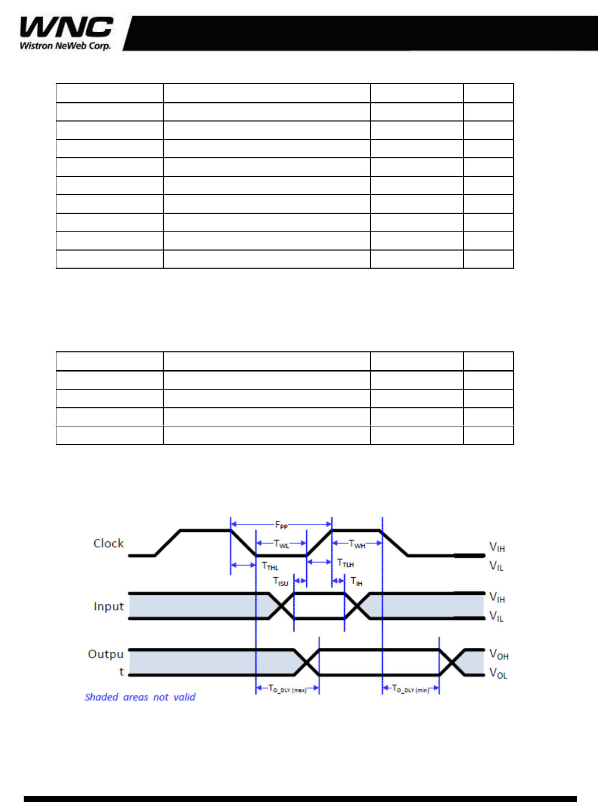
SPI slave interface electrical timing diagram
Fig.4: SPI salve timing
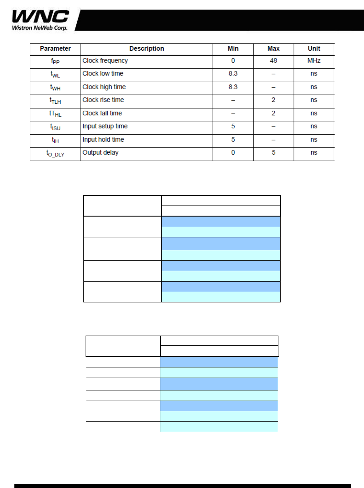
Table 4: SPI slave port timing (48 MHz reference clock)
The information contained herein is the exclusive property of WNC and shall not be distributed, reproduced, or disclosed in whole or in part without prior written permission of WNC. 10 / 15
DNSA-141 Specification
RF Tx target power [unit:dBm], IEEE mask and EVM compliance power.
Mode/Rate
MHz
2412~2472
11b 1Mbps
17
11b 11Mbps
17
11g 6Mbps
18
11g 54Mbps
14
11n HT20 MCS0
18
11n HT20 MCS7
13
11n HT40 MCS0
16
11n HT40 MCS7
12
RF Rx sensitivity [unit:dBm]:
Mode/Rate
MHz
2412~2472
11b 1Mbps
-92
11b 11Mbps
-85
11g 6Mbps
-88
11g 54Mbps
-71
11n HT20 MCS0
-87
11n HT20 MCS7
-67
11n HT40 MCS7
-64
The information contained herein is the exclusive property of WNC and shall not be distributed, reproduced, or disclosed in whole or in part without prior written permission of WNC. 11 / 15
DNSA-141 Specification
Antenna performance: on board printed ANT
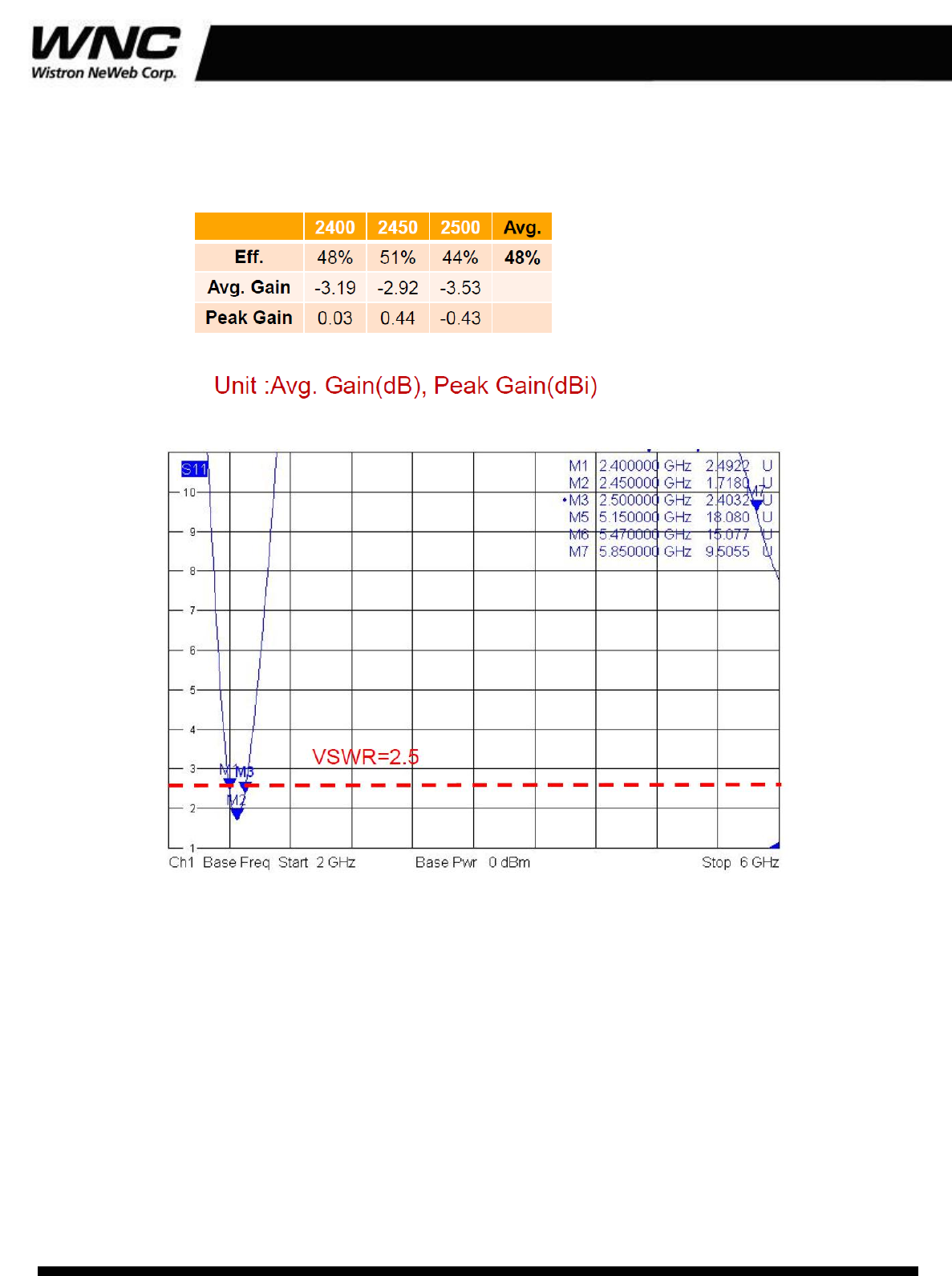
The on board printed antenna VSWR is better than 2.5 and efficiency is around 48%.
Fig.5 Antenna VSWR (Testing point is same as Fig.6)
The information contained herein is the exclusive property of WNC and shall not be distributed, reproduced, or disclosed in whole or in part without prior written permission of WNC. 12 / 15
DNSA-141 Specification
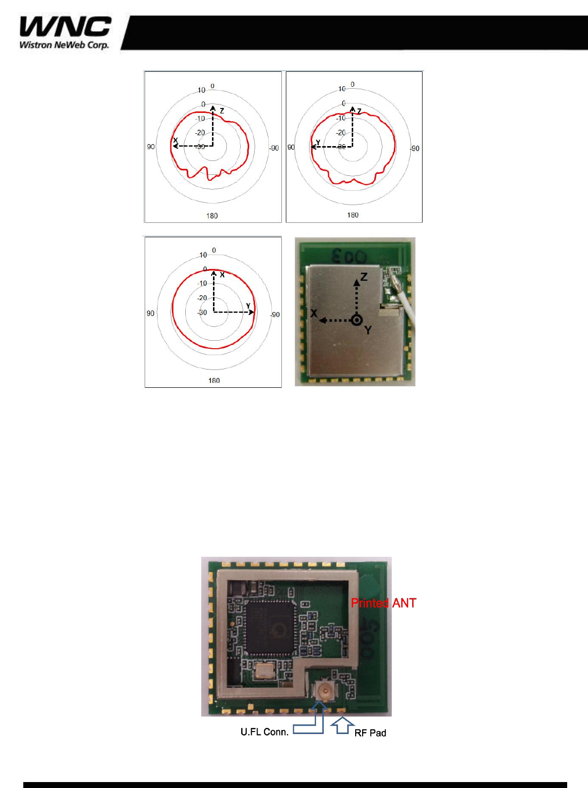
Fig.6: Antenna radiation pattern
RF path:
A. On board printed antenna: Please do not cover or put anything close to the antenna
otherwise the radiation efficiency will be degraded.
B. On board U.FL connector*1: optional.
C. RF PAD: Ideally, this can bridge the RF signal to the device outside the board. Application
board designer must be caution on the impedance control of the RF pad and 50 Ohm
trace at platform board.
D. DNSA-141 adopts printed antenna and U.FL conn. is no load in generic MP version.
Fig. 7: RF ports and on-board antenna (1pcs shielding in MP stage)
The information contained herein is the exclusive property of WNC and shall not be distributed, reproduced, or disclosed in whole or in part without prior written permission of WNC. 13 / 15
DNSA-141 Specification
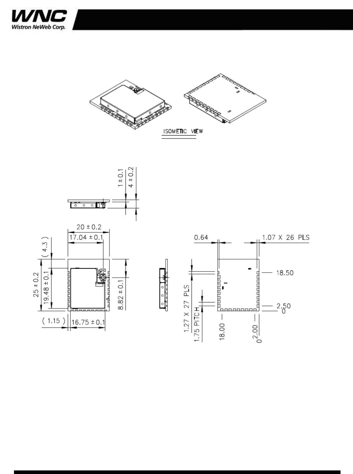
5. Mechanical Dimension and Drawing
Fig. 8: Mechanical drawing with shielding
Note: MP version default is without U.FL connector
The information contained herein is the exclusive property of WNC and shall not be distributed, reproduced, or disclosed in whole or in part without prior written permission of WNC. 14 / 15
DNSA-141 Specification
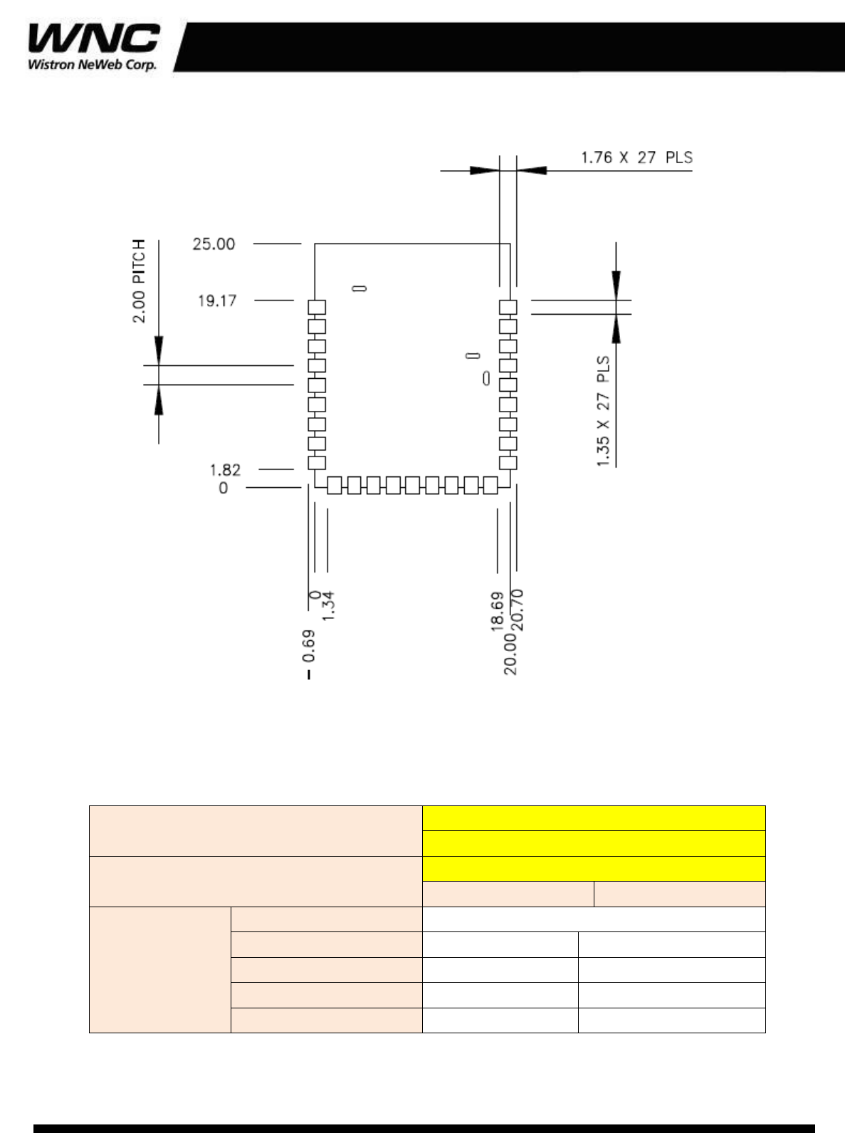
Recommend layout footprint for the application board
Fig. 9: Module Land Footprint
Soldering Reflow Profile: Using WNC’s internal SMT line profile. Solder paste: SAC305.
Profile Type Selection
Lead Free Solder
(Sn3.0Ag0.5Cu)
Lead Free
Temperature
Time
Profile Parameter
Setting
Max. Rising Slope
<3 ℃/sec
Soaking Time
140~190 ℃
70~105sec
Wetting Time
217 ℃
70~90sec
Peak Temperature
230~250 ℃
Over Wetting Time
230 ℃
40~60sec
Table 5: Reference soldering profile for customer to mount the module.
The information contained herein is the exclusive property of WNC and shall not be distributed, reproduced, or disclosed in whole or in part without prior written permission of WNC. 15 / 15
DNSA-141 Specification
6. Regulatory & Environment
Pre-certified FCC
Regulatory Compliance: IC & CE
Environment policy: All material used inside this module is Lead Free, RoHS compliant.
7. Package Information
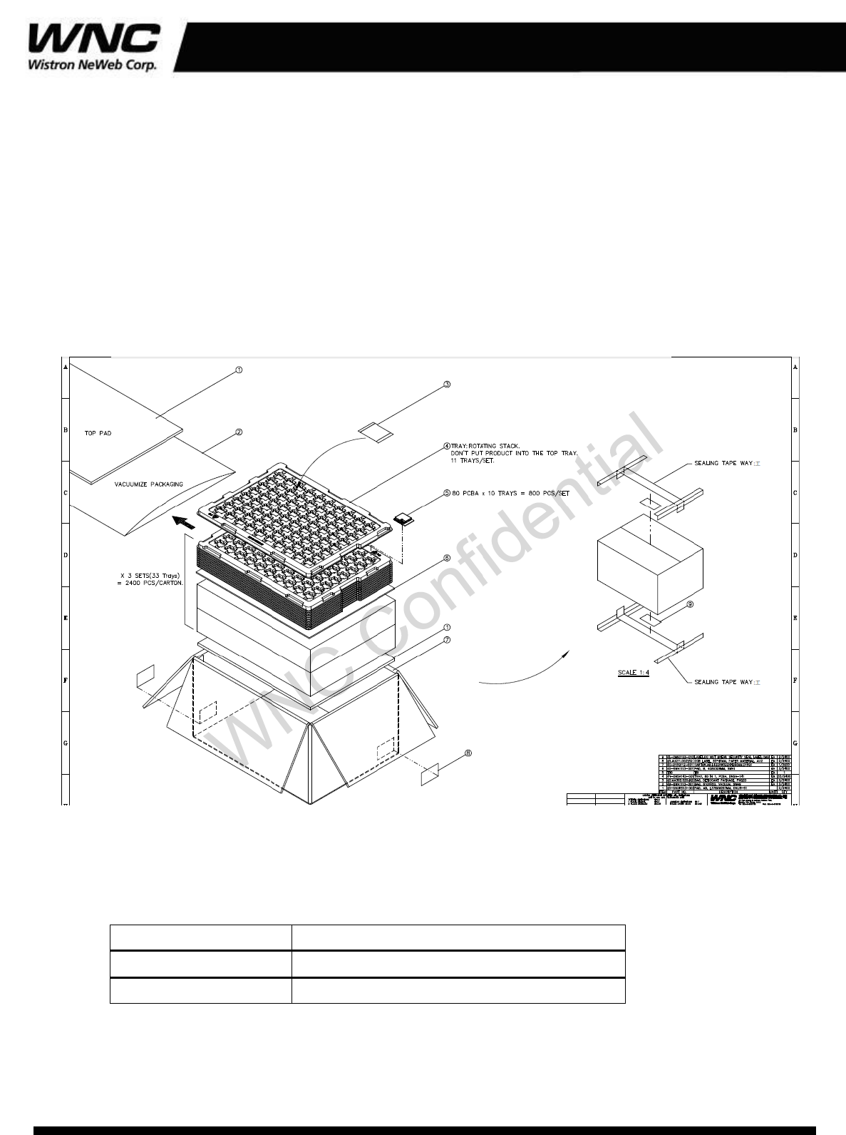
80 pcs DNSA-141 * 10 Trays = 800 pcs/SET
800 pcs * 3 SETS(33 Trays) = 2,400 pcs/CARTON
PS Tray Max. Temp is 75℃
Fig. 10: DNSA-141 Package Drawing
8. Order Information
Model
Description
DNSA-141(I)
I-temp standard, SPI, Printing ANT ver.
DNSA-141(I_UFL)
I-temp standard, SPI, U.FL antenna conn. ver.
Industry Canada statement:
This device complies with RSS-210 of the Industry Canada Rules. Operation is subject to the following
two conditions: (1) This device may not cause harmful interference, and (2) this device must accept any
interference received, including interference that may cause undesired operation.
Ce dispositif est conforme à la norme CNR-210 d'Industrie Canada applicable aux appareils radio
exempts de licence. Son fonctionnement est sujet aux deux conditions suivantes: (1) le dispositif ne doit
pas produire de brouillage préjudiciable, et (2) ce dispositif doit accepter tout brouillage reçu, y compris
un brouillage susceptible de provoquer un fonctionnement indésirable.
Radiation Exposure Statement:
This equipment complies with IC radiation exposure limits set forth for an uncontrolled environment.
This equipment should be installed and operated with minimum distance 20cm between the radiator &
your body.
Déclaration d'exposition aux radiations:
Cet équipement est conforme aux limites d'exposition aux rayonnements IC établies pour un
environnement non contrôlé. Cet équipement doit être installé et utilisé avec un minimum de 20 cm de
distance entre la source de rayonnement et votre corps.
This device is intended only for OEM integrators under the following conditions: (For module device use)
1) The antenna must be installed such that 20 cm is maintained between the antenna and users
2) The transmitter module may not be co-located with any other transmitter or antenna.
As long as 2 conditions above are met, further transmitter test will not be required. However, the OEM
integrator is still responsible for testing their end-product for any additional compliance requirements
required with this module installed.
Cet appareil est conçu uniquement pour les intégrateurs OEM dans les conditions suivantes: (Pour utilisation de
dispositif module)
1) L'antenne doit être installée de telle sorte qu'une distance de 20 cm est respectée entre l'antenne et les
utilisateurs
2) Le module émetteur peut ne pas être coïmplanté avec un autre émetteur ou antenne.
Tant que les 2 conditions ci-dessus sont remplies, des essais supplémentaires sur l'émetteur ne seront pas
nécessaires. Toutefois, l'intégrateur OEM est toujours responsable des essais sur son produit final pour
toutes exigences de conformité supplémentaires requis pour ce module installé.
IMPORTANT NOTE:
In the event that these conditions can not be met (for example certain laptop configurations or co-location
with another transmitter), then the Canada authorization is no longer considered valid and the IC ID can
not be used on the final product. In these circumstances, the OEM integrator will be responsible for
re-evaluating the end product (including the transmitter) and obtaining a separate Canada authorization.
NOTE IMPORTANTE:
Dans le cas où ces conditions ne peuvent être satisfaites (par exemple pour certaines configurations
d'ordinateur portable ou de certaines co-localisation avec un autre émetteur), l'autorisation du Canada
n'est plus considéré comme valide et l'ID IC ne peut pas être utilisé sur le produit final. Dans ces
circonstances, l'intégrateur OEM sera chargé de réévaluer le produit final (y compris l'émetteur) et
l'obtention d'une autorisation distincte au Canada.
End Product Labeling This transmitter module is authorized only for use in device where the antenna may
be installed such that 20 cm may be maintained between the antenna and users. The final end product
must be labeled in a visible area with the following: “Contains IC: 4441A-DNSA14”.
Plaque signalétique du produit final
Ce module émetteur est autorisé uniquement pour une utilisation dans un dispositif où l'antenne peut être
installée de telle sorte qu'une distance de 20cm peut être maintenue entre l'antenne et les utilisateurs. Le
produit final doit être étiqueté dans un endroit visible avec l'inscription suivante: "Contient des IC:
4441A-DNSA14".
Manual Information To the End User
The OEM integrator has to be aware not to provide information to the end user regarding how to install or
remove this RF module in the user’s manual of the end product which integrates this module.
The end user manual shall include all required regulatory information/warning as show in this manual.
Manuel d'information à l'utilisateur final
L'intégrateur OEM doit être conscient de ne pas fournir des informations à l'utilisateur final quant à la
façon d'installer ou de supprimer ce module RF dans le manuel de l'utilisateur du produit final qui intègre
ce module.
Le manuel de l'utilisateur final doit inclure toutes les informations réglementaires requises et
avertissements comme indiqué dans ce manuel.

Federal Communication Commission Interference Statement
This device complies with Part 15 of the FCC Rules. Operation is subject to the following two conditions:
(1) This device may not cause harmful interference, and (2) this device must accept any interference
received, including interference that may cause undesired operation.
This equipment has been tested and found to comply with the limits for a Class B digital device, pursuant
to Part 15 of the FCC Rules. These limits are designed to provide reasonable protection against harmful
interference in a residential installation. This equipment generates, uses and can radiate radio frequency
energy and, if not installed and used in accordance with the instructions, may cause harmful interference
to radio communications. However, there is no guarantee that interference will not occur in a particular
installation. If this equipment does cause harmful interference to radio or television reception, which
can be determined by turning the equipment off and on, the user is encouraged to try to correct the
interference by one of the following measures:
- Reorient or relocate the receiving antenna.
- Increase the separation between the equipment and receiver.
- Connect the equipment into an outlet on a circuit different from that
to which the receiver is connected.
- Consult the dealer or an experienced radio/TV technician for help.
FCC Caution: Any changes or modifications not expressly approved by the party responsible for
compliance could void the user's authority to operate this equipment.
This transmitter must not be co-located or operating in conjunction with any other antenna or
transmitter.
Radiation Exposure Statement:
This equipment complies with FCC radiation exposure limits set forth for an uncontrolled environment.
This equipment should be installed and operated with minimum distance 20cm between the radiator &
your body.
This device is intended only for OEM integrators under the following conditions:
1) The antenna must be installed such that 20 cm is maintained between the antenna and users
2) The transmitter module may not be co-located with any other transmitter or antenna.
As long as 2 conditions above are met, further transmitter test will not be required. However, the OEM
integrator is still responsible for testing their end-product for any additional compliance requirements
required with this module installed

IMPORTANT NOTE: In the event that these conditions can not be met (for example certain laptop
configurations or co-location with another transmitter), then the FCC authorization is no longer
considered valid and the FCC ID: NKR-DNSA141 can not be used on the final product. In these
circumstances, the OEM integrator will be responsible for re-evaluating the end product (including the
transmitter) and obtaining a separate FCC authorization.
End Product Labeling
This transmitter module is authorized only for use in device where the antenna may be installed such that
20 cm may be maintained between the antenna and users. The final end product must be labeled in a
visible area with the following: “Contains FCC ID: NKR-DNSA141”. The grantee's FCC ID can be used
only when all FCC compliance requirements are met.
Manual Information To the End User
The OEM integrator has to be aware not to provide information to the end user regarding how to install or
remove this RF module in the user’s manual of the end product which integrates this module.
The end user manual shall include all required regulatory information/warning as show in this manual.