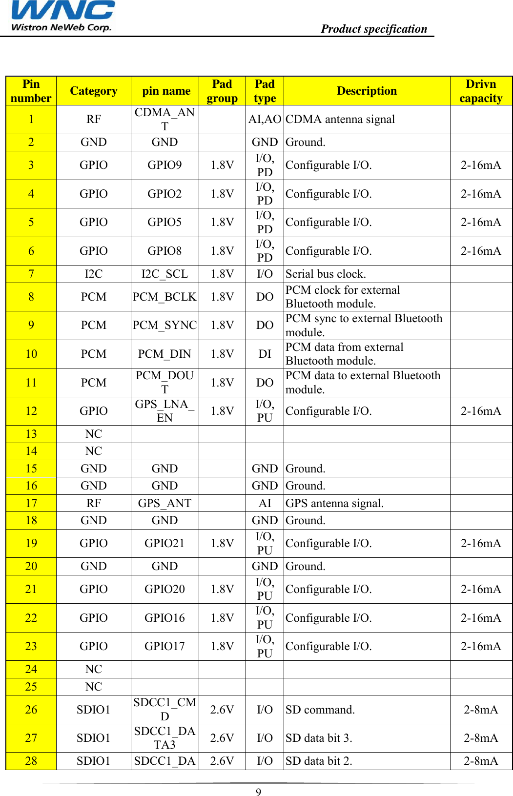
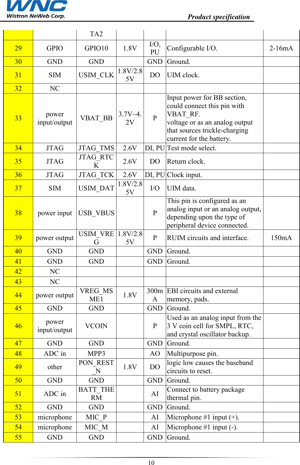
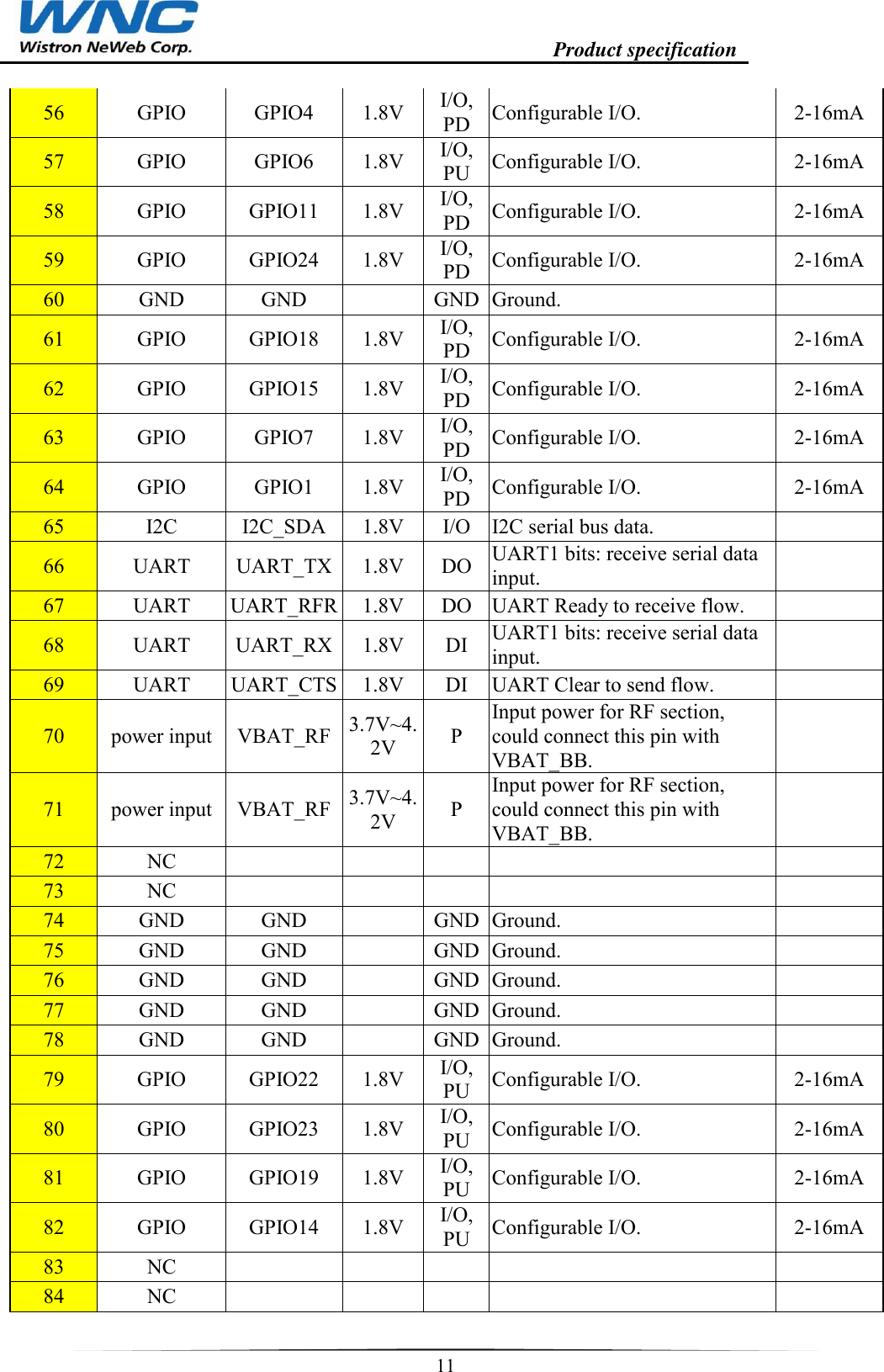
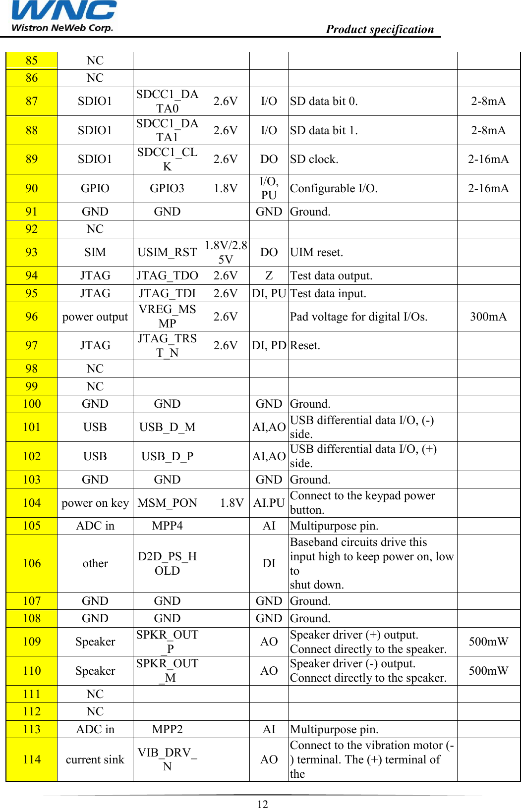
Wistron NeWeb UMC-6055Q module User Manual HiLo3G technical specification

Wistron NeWeb Corporation module HiLo3G technical specification

Users Manual

                                                                   Product specification    1    Wistron NeWeb Corp.          CONFIDENTIAL  THIS DOCUMENT CONTAINS PROPRIETARY TECHNICAL INFORMATION, WHICH IS THE PROPERTY OF THE WISTRON NEWEB CORPORATION AND SHALL NOT BE DISCLOSED TO OTHERS IN WHOLE OR IN PART, REPRODUCED, COPIED, OR USED AS THE BASIS FOR DESIGN, MANUFACTURING, OR SALE OF APPARATUS WITHOUT WRITTEN PERMISSION OF WISTRON NEWEB CORPORATION.  UMC-6055QV User Guide
                                                                   Product specification    2   CONTENTS   CONTENTS .......................................................................................................................................................................... 2 1. INTRODUCTION ...................................................................................................................................................... 3 1.1 PRODUCT CONCEPT ........................................................................................................................................ 3 1.2 STANDARDS ....................................................................................................................................................... 3 1.3 TERMS AND ABBREVIATION ......................................................................................................................... 4 1.4 CONVENTIONS ................................................................................................................................................... 4 1.5 PRODUCT FEATURES OVERVIEW ............................................................................................................... 4 2. BLOCK DIAGRAM & PIN ASSIGNMENT ........................................................................................................... 7 3. RF AIR INTERFACES AND PERFORMANCE ................................................................................................ 14 3.1 RF AIR INTERFACE AND BAND CONFIGURATION ................................................................................ 14 3.1.1 Air interfaces ............................................................................................................................................. 14 3.2 RF PERFORMANCE ......................................................................................................................................... 14 3.3 TRANSMITTER POWER CLASS ................................................................................................................... 14 4. OPERATING CONDITIONS ................................................................................................................................ 15 4.1 ABSOLUTE MAXIMUM RATINGS ................................................................................................................. 15 4.2 RECOMMENDED OPERATING CONDITION .............................................................................................. 16 5. CURRENT CONSUMPTION ................................................................................................................................ 17 6. APPLCATION DESIGN NOTES ......................................................................................................................... 18 6.1  LAYOUT NOTES .................................................................................................................................. 18 6.2  RF PIN INPUT IMPEDANCE MATCHING ........................................................................................... 18 6.3 HANDING REQUIREMENTS .......................................................................................................................... 18 6.4 SOLDING REQUIREMENTS ........................................................................................................................... 18 7. MECHANICAL REQUIREMENTS ...................................................................................................................... 20 7.1 MODULE DIMENSION AND FOOTPRINT.................................................................................................... 20 8. CERTIFICATION REQUIREMENTS ................................................................................................................ 22 8.1 CARRIER CERTIFICATION REQUIREMENTS ........................................................................................... 22 8.2 REGULATORY COMPLIANCE  ..................................................................................................................... 22 8.3 FCC WARNING STATEMENT ........................................................................................................................ 22       Revision history   Revision  Date Description V1.0 April 7 2014 Initial release V2.0 May 13 2014 Modify recommended operating condition
                                                                   Product specification    3  1.  INTRODUCTION This document describes the hardware interface of the WNC Small Form Factor (SFF) module used to connect the device application and the air interface.  Two versions of Small Form Factor (SFF) module are described in this specification document as follows:     UMC-6055QV - CDMA2000 1X  1.1  PRODUCT CONCEPT The SFF module is one of the smallest available CDMA2000 1X modules of the market. The target application is  the  Machine  to  Machine  (M2M)  market  including  automotive,  AMM  (Automatic  Metering  Management), tracking system, Alarm, Healthcare/monitoring, Telematics etc. Despite its small size and cost,   In addition to its size it has the following outstanding characteristics:   Minimum low power consumption in idle mode: 1.4mA   High input voltage range: 3.4 V to 4.2 V   USB High Speed   Digital Audio PCM   Full set of AT commands as well as analogue and Digital audio interface.   In addition to the module, a complete development kit can be provided for customers. 1.2  STANDARDS This product, together with its evaluation board, is in compliance with the directives and standards listed below:  Directives  FCC RF : FCC Part 22H (850 Band )          FCC Part 24E (for 1900 Band) FCC Part 22 Subpart H:  Cellular Radiotelephone Service; Subpart I: Offshore Radiotelephone Service;   FCC Part 24 E: Personal Communications Service; Subpart E: Broadband PCS.  EMI: FCC Part 15B Subpart B - Radio frequency devices subpart B – Unintentional Radiators SAR(MPE) : OET65C
                                                                   Product specification    4  1.3  TERMS AND ABBREVIATION ADC      Analog to Digital Converter CODEC    Coder-Decoder CLIP      Calling Line Identification Presentation  COLP      Connected Line Identification Presentation  CLIR      Calling Line Identification Restriction  COLR      Connected Line Identification Restriction  CTS      Clear To Send CSD      Circuit Switched Data CS      Codec Scheme DSR      Data Set Ready ENS      Enhanced network selection  EONS      Enhanced operator name string ESD      Electrostatic Discharge ETS      European Telecommunication Standard FAX      Facsimile IC      Integrated Circuit IEEE      Institute of Electrical and Electronics Engineers I/O      Input / Output ISO      International Standards Organization ITU      International Telecommunication Union JTAG      Joint Test Action Group Kbps      kilobit per second LCD      Liquid Crystal Display LED      Light Emitting Diode Mbps      Megabit per second PCB      Printed Circuit Board PCM      Pulse Code Modulation PCS      Personal Communication System PWM      Pulse Width Modulation RAM      Random Access Memory RF      Radio Frequency RI      Ring Indication RMS      Root Mean Square RTS      Ready To Send RX      Reception SMS      Short Message Service TBC      To Be Confirmed TBD      To Be Defined TX      Transmission UART      Universal Asynchronous Receiver and Transmitter USB      Universal Serial Bus USSD      Unstructured Supplementary Service Data 1.4  CONVENTIONS Throughout this document, DTE (data terminal equipment) indicates the equipment which masters and controls the module device by sending AT commands via its serial interface. DCE (data communication equipment) indicates the module device.  1.5  PRODUCT FEATURES OVERVIEW  Temperature range Operation Temperature: -25°C to +85°C  Storage: -40°C to +85°C Weight  6 g (typ.) ESD ESD protection >= 2 kV
                                                                   Product specification    5  Physical dimensions 22.1 x 25.1 x 2.65 mm (typical) Connection 141 pin LGA type Power supply 3.4V to 4.2V range, 3.8V nominal  Power consumption* Off mode: 50 µA typical  Registered idle mode:   CDMA2000: 1.3 mA  Peak Current   CDMA2000: up to 700 mA   Antenna /RF interface Both GPS and transmitter/receiver RF are LGA Pad. Frequency bands UMC-6055QV  module supports CDMA2000 BC0/BC1  Transmit power Class 3 for CDMA2000 BC0/BC1 PWM Signal for LED, vibrating device and Buzzer management is provided on the PWM pin Digital audio link A digital audio interface PCM bus is provided. Master mode with 16 bits and a frequency of 2048 KHz. Data/command multiplexing  Software management of data/command multiplexing on the serial link UART. USB Supports USB High speed 480Mbps and full speed 12Mbps, with 3 logical Channels. Battery charging is achieved through USB           Module Hardware Configuration  The SFF LGA module will support the QSC6055 chipset with the configuration described below.  For UMC-6055QV module: Key Features                                                            •  Compliant with 3GPP for CDMA 1xRTT  •  Max. Data Rate : 153kbps FL; 153kbps RL  •  Support OS: Brew Mobile Platform  •  ARM9 operating at 192Mhz maximum frequency •  Data interface: USB2.0 Host High Speed •  Form Factor: LGA module  Specification       •  Communication Interface: (I2C x1/UART x1/USB2.0 x1/SDIO x1)  •  Supported SIM cards (3V and 1.8V SIM cards) •  General purpose I/O pins ( x25 )  •  Audio Interface (PCM/ I2S)         •  MCP (DDR 512Mb + 1Gb NAND)    •  Support GPS           •  RF interface: 2 RF pads for CDMA TX/RX, and GPS.      CDMA2000 Support Bands  •  Band BC0                                                            * The power consumption is highly dependent on the customer’s product design and the module environment.
                                                                   Product specification    6  •  Band BC1
                                                                   Product specification    7  2.  BLOCK DIAGRAM & PIN ASSIGNMENT          Pin Definition 4 This section is intended to capture the final LGA pin out for the SFF Module. The interfaces with a SFF module are all through a 141-pin surface LGA pad, as shown in Figure 2-1.
                                                                   Product specification    8   For UMC-6055QV module:  Figure 2-1: UMC-6055QV module
                                                                   Product specification    9    Pin number Category  pin name Pad group Pad type Description Drivn capacity 1 RF CDMA_ANT   AI,AO CDMA antenna signal   2 GND GND   GND Ground.   3 GPIO GPIO9 1.8V I/O, PD Configurable I/O. 2-16mA 4 GPIO GPIO2 1.8V I/O, PD Configurable I/O. 2-16mA 5 GPIO GPIO5 1.8V I/O, PD Configurable I/O. 2-16mA 6 GPIO GPIO8 1.8V I/O, PD Configurable I/O. 2-16mA 7 I2C I2C_SCL 1.8V I/O Serial bus clock.   8 PCM PCM_BCLK 1.8V DO PCM clock for external Bluetooth module.   9 PCM PCM_SYNC 1.8V DO PCM sync to external Bluetooth module.   10 PCM PCM_DIN 1.8V DI PCM data from external Bluetooth module.   11 PCM PCM_DOUT 1.8V DO PCM data to external Bluetooth module.   12 GPIO GPS_LNA_EN 1.8V I/O, PU Configurable I/O. 2-16mA 13 NC           14 NC           15 GND GND   GND Ground.   16 GND GND   GND Ground.   17 RF GPS_ANT   AI GPS antenna signal.   18 GND GND   GND Ground.   19 GPIO GPIO21 1.8V I/O, PU Configurable I/O. 2-16mA 20 GND GND   GND Ground.   21 GPIO GPIO20 1.8V I/O, PU Configurable I/O. 2-16mA 22 GPIO GPIO16 1.8V I/O, PU Configurable I/O. 2-16mA 23 GPIO GPIO17 1.8V I/O, PU Configurable I/O. 2-16mA 24 NC           25 NC           26 SDIO1 SDCC1_CMD 2.6V I/O SD command. 2-8mA 27 SDIO1 SDCC1_DATA3 2.6V I/O SD data bit 3. 2-8mA 28 SDIO1 SDCC1_DA2.6V I/O SD data bit 2. 2-8mA
                                                                   Product specification    10  TA2 29 GPIO GPIO10 1.8V I/O, PU Configurable I/O. 2-16mA 30 GND GND   GND Ground.   31 SIM USIM_CLK 1.8V/2.85V DO UIM clock.   32 NC           33 power input/output VBAT_BB 3.7V~4.2V P Input power for BB section, could connect this pin with VBAT_RF. voltage or as an analog output that sources trickle-charging current for the battery.   34 JTAG JTAG_TMS 2.6V DI, PU Test mode select.   35 JTAG JTAG_RTCK 2.6V DO Return clock.   36 JTAG JTAG_TCK 2.6V DI, PU Clock input.   37 SIM USIM_DAT 1.8V/2.85V I/O UIM data.   38 power input USB_VBUS   P This pin is configured as an analog input or an analog output, depending upon the type of peripheral device connected.   39 power output USIM_VREG 1.8V/2.85V P RUIM circuits and interface. 150mA 40 GND GND   GND Ground.   41 GND GND   GND Ground.   42 NC           43 NC           44 power output VREG_MSME1 1.8V 300mA EBI circuits and external memory, pads.   45 GND GND   GND Ground.   46 power input/output VCOIN   P Used as an analog input from the 3 V coin cell for SMPL, RTC, and crystal oscillator backup.   47 GND GND   GND Ground.   48 ADC in MPP3   AO Multipurpose pin.   49 other PON_REST_N 1.8V DO logic low causes the baseband circuits to reset.   50 GND GND   GND Ground.   51 ADC in BATT_THERM   AI Connect to battery package thermal pin.   52 GND GND   GND Ground.   53 microphone MIC_P   AI Microphone #1 input (+).   54 microphone MIC_M   AI Microphone #1 input (-).   55 GND GND   GND Ground.
                                                                   Product specification    11  56 GPIO GPIO4 1.8V I/O, PD Configurable I/O. 2-16mA 57 GPIO GPIO6 1.8V I/O, PU Configurable I/O. 2-16mA 58 GPIO GPIO11 1.8V I/O, PD Configurable I/O. 2-16mA 59 GPIO GPIO24 1.8V I/O, PD Configurable I/O. 2-16mA 60 GND GND   GND Ground.   61 GPIO GPIO18 1.8V I/O, PD Configurable I/O. 2-16mA 62 GPIO GPIO15 1.8V I/O, PD Configurable I/O. 2-16mA 63 GPIO GPIO7 1.8V I/O, PD Configurable I/O. 2-16mA 64 GPIO GPIO1 1.8V I/O, PD Configurable I/O. 2-16mA 65 I2C I2C_SDA 1.8V I/O I2C serial bus data.   66 UART UART_TX 1.8V DO UART1 bits: receive serial data input.   67 UART UART_RFR 1.8V DO UART Ready to receive flow.   68 UART UART_RX 1.8V DI UART1 bits: receive serial data input.   69 UART UART_CTS 1.8V DI UART Clear to send flow.   70 power input VBAT_RF 3.7V~4.2V P Input power for RF section, could connect this pin with VBAT_BB.   71 power input VBAT_RF 3.7V~4.2V P Input power for RF section, could connect this pin with VBAT_BB.   72 NC           73 NC           74 GND GND   GND Ground.   75 GND GND   GND Ground.   76 GND GND   GND Ground.   77 GND GND   GND Ground.   78 GND GND   GND Ground.   79 GPIO GPIO22 1.8V I/O, PU Configurable I/O. 2-16mA 80 GPIO GPIO23 1.8V I/O, PU Configurable I/O. 2-16mA 81 GPIO GPIO19 1.8V I/O, PU Configurable I/O. 2-16mA 82 GPIO GPIO14 1.8V I/O, PU Configurable I/O. 2-16mA 83 NC           84 NC
                                                                   Product specification    12  85 NC           86 NC           87 SDIO1 SDCC1_DATA0 2.6V I/O SD data bit 0. 2-8mA 88 SDIO1 SDCC1_DATA1 2.6V I/O SD data bit 1. 2-8mA 89 SDIO1 SDCC1_CLK 2.6V DO SD clock. 2-16mA 90 GPIO GPIO3 1.8V I/O, PU Configurable I/O. 2-16mA 91 GND GND   GND Ground.   92 NC           93 SIM USIM_RST 1.8V/2.85V DO UIM reset.   94 JTAG JTAG_TDO 2.6V Z Test data output.   95 JTAG JTAG_TDI 2.6V DI, PU Test data input.   96 power output VREG_MSMP 2.6V   Pad voltage for digital I/Os. 300mA 97 JTAG JTAG_TRST_N 2.6V DI, PD Reset.   98 NC           99 NC           100 GND GND   GND Ground.   101 USB USB_D_M   AI,AO USB differential data I/O, (-) side.   102 USB USB_D_P   AI,AO USB differential data I/O, (+) side.   103 GND GND   GND Ground.   104 power on key MSM_PON  1.8V AI.PU Connect to the keypad power button.   105 ADC in MPP4   AI Multipurpose pin.   106 other D2D_PS_HOLD   DI Baseband circuits drive this input high to keep power on, low to shut down.   107 GND GND   GND Ground.   108 GND GND   GND Ground.   109 Speaker SPKR_OUT_P   AO Speaker driver (+) output. Connect directly to the speaker. 500mW 110 Speaker SPKR_OUT_M   AO Speaker driver (-) output. Connect directly to the speaker. 500mW 111 NC           112 NC           113 ADC in MPP2   AI Multipurpose pin.   114 current sink VIB_DRV_N   AO Connect to the vibration motor (-) terminal. The (+) terminal of the
                                                                   Product specification    13  motor connects to VDD. 115 ADC in PA_THERM   AI Connect to thermistor for PA.   116 current sink LCD_DRV_N   AO LCD backlight current driver. 150mA 117 GND GND   GND Ground.   118 GPIO GPIO13 1.8V I/O, PD Configurable I/O. 2-16mA 119 GPIO GPIO0 1.8V I/O, PD Configurable I/O. 2-16mA 120 GPIO GPIO12 1.8V I/O, PD Configurable I/O. 2-16mA 121 PWM GP_PDM_0 1.8V DO,PD "Backlight"12-bit PDM;XO/4 clock. 2-16mA 122 GND GND   GND Ground.   123 GND GND   GND Ground.   124 GND GND   GND Ground.   125 GND GND   GND Ground.   126 GND GND   GND Ground.   127 GND GND   GND Ground.   128 GND GND   GND Ground.   129 GND GND   GND Ground.   130 GND GND   GND Ground.   131 GND GND   GND Ground.   132 GND GND   GND Ground.   133 GND GND   GND Ground.   134 GND GND   GND Ground.   135 GND GND   GND Ground.   136 GND GND   GND Ground.   137 GND GND   GND Ground.   138 GND GND   GND Ground.   139 GND GND   GND Ground.   140 GND GND   GND Ground.   141 GND GND   GND Ground.
                                                                   Product specification    14  3.  RF AIR INTERFACES AND PERFORMANCE 3.1   RF AIR INTERFACE AND BAND CONFIGURATION 3.1.1  Air interfaces UMC-6055QV module supports CDMA 1xRTT and GPS 3.2   RF PERFORMANCE The UMC-6055QV modules RF transmitter/receiver is fully compliant with the applicable standards. The sensitivity and max output power are listed in Table 3-2-1 and Table 3-2-2  Specification Min Typ Max Units CDMA2000 1X  Sensitivity           BC1 (1930-1990MHz Rx) -104.7 -108   dBm   BC0 (869-894MHz Rx) -106.7 -110   dBm      GPS Sensitivity   -155   dBm  Table 3-2-1 Conducted Receiver Sensitivity  Specification Min Typ Max Units CDMA2000 1X Output Power           BC1 (1850-1910MHz Tx)   23.5   dBm   BC0 (824-849MHz Tx)   23.5   dBm      GPS Sensitivity   -155   dBm  Table 3-2-2 Conducted Transmitter Max Output Power 3.3  TRANSMITTER POWER CLASS The UMC-6055QV Modules support the power classes listed in Table 3-3  Mode Band Power Class CDMA2000 1X BC1/BC0 3  Table 3-3 Supported Power Classes
                                                                   Product specification    15  4.  OPERATING CONDITIONS                                                                                                                                                                                                                                                                                                                               4.1  ABSOLUTE MAXIMUM RATINGS  Operating  UMC-6055QV  Modules  under  conditions  beyond  its  absolute  maximum  ratings  (Table  4-1)  may damage the device. Absolute maximum ratings are limiting values to be considered individually when all other parameters are within their specified operating ranges. Functional operation and specification compliance under any absolute maximum condition, or after exposure to any of these conditions, is not guaranteed or implied. Exposure may affect device reliability.  Symbol Parameter Min Max Unit Ts Storage temperature -40 85 C USB_VBUS DC power supply voltage 4.5 5.5 V VBAT Battery input voltage 3.4 4.2 V VESD_HBM Eletrostatic discharging voltage rating (human body model) * V VESD_CDM Electrostatic discharge voltage rating (charge device model) * V RH_Operating Operating humidity range 10 90 % RH_Non-OP Nonoperating humidity range 5 95 % *NOTE: ESD protection should be provided external to the module.                                                   Table 4-1 : Absolute maximum ratings
                                                                   Product specification    16  4.2  RECOMMENDED OPERATING CONDITION The devices meet all performance specifications when used within the recommended operating conditions as described in Table 4-2  Symbol Parameter Min Typ. Max Unit T Operating Temperature  -25  +85    Normal operating temperature range  See section 4.2.1  -20  +65    Extended operating temperature range 1  See section 4.2.2  -25  -20    Extended operating temperature range 2  See section 4.2.3  +65  +85   USB_VBUS DC Power Supply Voltage 4.75 5 5.25 V VBAT (Battery) DC Power Supply Voltage 3.4 3.8 4.2 V Table 4-2  4.2.1 Normal operating temperature range  The wireless module is fully functional and meets the 3GPP specification across the specified temperature range.   4.2.2 Extended operating temperature range 1  The wireless module is fully functional across the specified temperature range. Occasional deviations from the 3GPP specification may occur.   4.2.3 Extended operating temperature range 2  The wireless module is functional across the specified temperature range. Occasional deviations from the 3GPP specification may occur. Thermal protection including automatic shutdown is implemented for protection against overheating.
                                                                   Product specification    17  5.  CURRENT CONSUMPTION The specified supply currents in Table 5-1 are based operation at room temperature. Current measurements are taken with default parameter settings, nominal supply voltage. The DUT is mounted on a module test board and the accelerometer on, unless otherwise noted.  Operating Modes  Description  Conditions Average Current  Min Typ Max Unit  Power Down(OFF) VBAT voltage applied  Power Down*1,2   22   µA  CDMA2000 1X Between Rx wakeups  Sleep*1,2   1   mA    Rx awake current  Rx Idle   70   mA  Average Sleep and Rx  Standby*3   1.4   mA  Average GPS only  Average GPS only    42  mA    TX/RX (0dBm)    180  mA    Tx/Rx (23.5dBm)    550  mA      Table 5-1 Typical Power Consumption  Note 1 Measurement taken without Test Board  Note 2 Measurement taken without Accelerometer  Note 3 Value calculated from measured IUSB_AVG subtacted from  ITOTAL_GPS_AVG, I-GPS = I-Total_GPS_AVG – IUSB_AVG
                                                                   Product specification    18  6.  APPLICATION DESIGN NOTES 6.1 Layout Notes 6.2 RF Pin Input Impedance Matching Applications utilizing the module must ensure that a 50Ω controlled impedance trace is used. Shown in the accompanying table are example calculations for a four- layer FR4 stack up and the resulting trace width for Bluetooth RF input. The figure below illustrates the layer stack up for a four- layer board according to the Description column in the table below.  Layer Material Type Dielectric Thickness Trace Width Copper Thickness Dielectric Constant Char. Impedance Description 1 Conductive - 27 2.1 - 50 Microstrip Dielectric 16 - - 4.3 - Prepreg 2 Conductive - - 1.4  - Plane Dielectric 20   4.3 - Prepreg 3 Conductive - - 1.4 - - Plane Dielectric 16 - - 4.3 - Prepreg 4 Conductive - 27 2.1 - 50 Microstrip Table 6-1-1-1 Application Board Characteristic Impedance   Figure 6-1-1-1 Application Board Layer Stack Up  6.3 Handling Requirements DO NOT TOUCH ANY Pad OF BTI MODULE WHILE ASSEMBLYING.  6.4 Soldering Requirements  Soldering Iron Soldering  Solder Temperature: 350oC Immersion Duration: 2 ~ 3 seconds
                                                                   Product specification    19  6.1.3 Reflow Profile
                                                                   Product specification    20  7.  MECHANICAL REQUIREMENTS 7.1 Module Dimension and Footprint The dimension of this module:                   Figure 7-1-1 Dimension of SFF Module
                                                                   Product specification    21    Figure 7-1-2 Recommended Footprint of SFF Module
                                                                   Product specification    22  8 Certification Requirements  8.1 Carrier Certification Requirements  The SFF Development Kit will be used to demonstrate Safe for Network (SFN) compliance for the SFF module on selected cellular carriers.  8.2  Regulatory Compliance 5    8.3  FCC warning statement FCC Regulations:  This device complies with Part 15 of the FCC Rules. Operation is subject to the following two conditions: (1) This device may not cause harmful interference, and (2) this device must accept any interference received, including interference that may cause undesired operation.  This equipment has been tested and found to comply with the limits for a Class B digital device, pursuant to Part 15 of the FCC  Rules.    These  limits  are  designed  to  provide  reasonable  protection  against  harmful  interference  in  a  residential installation.  This  equipment  generates,  uses  and  can  radiate  radio  frequency  energy  and,  if  not  installed  and  used  in accordance with the instructions, may cause harmful interference to radio communications.  However, there is no guarantee that interference will not occur in a particular installation.  If this equipment does cause harmful interference to radio or television reception, which can be determined by turning the equipment off and on, the user is encouraged to try to correct the interference by one of the following measures:  -  Reorient or relocate the receiving antenna. -  Increase the separation between the equipment and receiver. -  Connect the equipment into an outlet on a circuit different from that to which the receiver is connected. -  Consult the dealer or an experienced radio/TV technician for help.  FCC Caution: Any changes or modifications not expressly approved by the party responsible for compliance could void the user's authority to operate this equipment.  This transmitter must not be co-located or operating in conjunction with any other antenna or transmitter.
                                                                   Product specification    23  Radiation Exposure Statement: This equipment complies with FCC radiation exposure limits set forth for an uncontrolled environment. This equipment should be installed and operated with minimum distance 20cm between the radiator & your body.  This device is intended only for OEM integrators under the following conditions:  1) The antenna must be installed such that 20 cm is maintained between the antenna and users, and the antenna typeand gain allowed for use with this device is type: fixed external; max. gain: 2dBi.  2) The transmitter module may not be co-located with any other transmitter or antenna.   As long as 2 conditions above are met, further transmitter test will not be required. However, the OEM integrator is still responsible for testing their end-product for any additional compliance requirements required with this module installed  IMPORTANT NOTE: In the event that these conditions can not be met (for example certain laptop configurations or co-location with another transmitter), then the FCC authorization is no longer considered valid and the FCC ID can not be used on the final product. In these circumstances, the OEM integrator will be responsible for re-evaluating the end product (including the transmitter) and obtaining a separate FCC authorization.  End Product Labeling This transmitter module is authorized only for use in device where the antenna may be installed such that 20 cm may be maintained between the antenna and users. The final end product must be labeled in a visible area with the following: “Contains FCC ID: NKRUMC-6055Q”. The grantee's FCC ID can be used only when all FCC compliance requirements are met.  Manual Information To the End User The OEM integrator has to be aware not to provide information to the end user regarding how to install or remove this RF module in the user’s manual of the end product which integrates this module. The end user manual shall include all required regulatory information/warning as show in this manual.

Navigation menu