Wistron NeWeb UWMWBT-CWM01 MOD-SM WNC BLUETOOTH/WLAN CWM-01 User Manual WBT Manual for FCC 20111227
Wistron NeWeb Corporation MOD-SM WNC BLUETOOTH/WLAN CWM-01 WBT Manual for FCC 20111227
User Manual
The information contained herein is the exclusive property of WNC and shall not be distributed, reproduced, or disclosed in whole or in part without prior written permission of WNC. 1 / 30
W
LAN/BT System Integration Manual
ModelName:
UMW‐WBT,
CWM‐01
IssueDate:
2011/05/05
ProjectCode: RevDate:
2011/12/27
WLAN/BT
SystemIntegrationManual
BaseModel:Rev:2

The information contained herein is the exclusive property of WNC and shall not be distributed, reproduced, or disclosed in whole or in part without prior written permission of WNC. 2 / 30
W
LAN/BT System Integration Manual
RevisionHistory
Rev.HistoryDateAuthor
1- Initialversion2011/05/05ShukaiHsu
HTLiao
HausonChen
ChrisWJHuang
21.Frequencyrangeischangedto2400‐2483.5Mhz
2. FCCchannelsrevisedtobech1–ch11
3. Powervalueisrevised:
WIFI:15+/‐1.5dBm
BT:class1
-
2011/12/27Shukai
-
-
-

The information contained herein is the exclusive property of WNC and shall not be distributed, reproduced, or disclosed in whole or in part without prior written permission of WNC. 3 / 30
W
LAN/BT System Integration Manual
TABLEOFCONTENTS
1. INTRODUCTION ................................................................................................................................................................4
1.1 Product Overview.............................................................................................................................................................4
1.3 Standard Bluetooth Profiles..............................................................................................................................................6
1.4 Temperature Parameter.....................................................................................................................................................6
1.5 Module Pin Out ................................................................................................................................................................7
1.6 Power management ..........................................................................................................................................................9
1.7 RF connection ................................................................................................................................................................10
2. INTERFACES .................................................................................................................................................................... 11
2.1 SDIO Interface ...............................................................................................................................................................11
2.2 UART Interface ..............................................................................................................................................................12
2.2.1SignalBehavior ....................................................................................................................................................12
2.3 Digital Audio Interface...................................................................................................................................................13
2.4 RESET#..........................................................................................................................................................................14
2.5 SLEEP_CLK ..................................................................................................................................................................14
2.6 Joint Test Action Group (JTAG) and Test Interface........................................................................................................14
JTAGInterfaceSignalDescription .................................................................................................................................14
2.7 Antenna Diagnosis..........................................................................................................................................................15
HandlingRequirements ................................................................................................................................................24
Moisturepreconditioning.............................................................................................................................................24
4.2 Soldering Requirements .................................................................................................................................................24
4.2.1SolderingIronSoldering ......................................................................................................................................24
4.2.2ReflowProfile ......................................................................................................................................................24
4.2.3SolderingPaste ....................................................................................................................................................25
4.2.4 PCB Layout Footprint Design .............................................................................................................................26
5 PRODUCT TESTING.............................................................................................................................................................28
5.1 Production test................................................................................................................................................................28
FORPRODUCTAVAILABLEINTHEUSA/CANADAMARKET,ONLYCHANNEL1~11CANBEOPERATED.SELECTIONOFOTHER
CHANNELSISNOTPOSSIBLE........................................................................................................................................................29

The information contained herein is the exclusive property of WNC and shall not be distributed, reproduced, or disclosed in whole or in part without prior written permission of WNC. 4 / 30
W
LAN/BT System Integration Manual
1.Introduction
Thisdocumentspecifiesthemechanicalandelectricalspecificationsforthe802.11b/gWiFiand
Bluetooth3.0module.Continuingatraditionofdesigningenuityanddevelopment,WistronNeWeb
Corporation(WNC)presentsastandardmodularsolutionforWiFiandBluetoothtechnologytocomply
withOEMindustrialrequirementsinvehicles.Themoduleprovides802.11b/gWLANandBluetooth3.0
functionsbyusingasinglechipsetsolution.Utilizingthemodule,radiomanufacturersareenabledto
createfeaturerichreadydesignwithouttheadditionalburdentoredesigntheWiFiandBluetooth
functions.
Fortheremainderofthedocument,thehostdesignthatshallintegratethemoduleshallbe
referredtoastheapplication.Theapplicationshallbethecontrollinghostentitywithrespecttothe
module.
Thisdocumentalsoprovideshardwaredesigninstructionandproductionsetupinformation.
1.1ProductOverview
Thisdocumentspecifiesthe802.11b/g+BluetoothModule.Thespecificationcoversoverall
dimensions,generalmoduleconstruction,connectorinterfacefootprints,andmechanicalandelectrical
characteristicsoftheWNC’s802.11b/g+Bluetoothmodule.ThismodulewasbuiltbyusingMarvell’s
88W8688chipset.
HostInterface:
WLAN:SDIO
Bluetooth:SDIO/highspeedUART
802.11b/g:
Frequencyband:
BMode:2.400~2.4835GHz
GMode:2.400~2.4835GHz
ChannelSpacing:
B/GMode:5MHz
Modulation:
BMode:DSSSwithDBPSK,DQPSK,andCCK
GMode:OFDMwithBPSK,QPSK,QAM,and16/64QAM
ChannelsSupport:
BMode: CH1–CH13(ETSI)/CH1‐CH11(FCC)/CH1‐CH14(Japan)
GMode: CH1–CH13(ETSI)/CH1‐CH11(FCC)/CH1‐CH14(Japan)
RFoutputPower:
BMode:16.30dBm@1,2,5.5,and11Mbps
GMode:23.55dBm@6,9,12,18,24,36,48and54Mbps

The information contained herein is the exclusive property of WNC and shall not be distributed, reproduced, or disclosed in whole or in part without prior written permission of WNC. 5 / 30
W
LAN/BT System Integration Manual
Sensitivity:
BMode:–88dBmat1Mbps
–87dBmat2Mbps
–84dBmat5.5Mbps
–80dBmat11Mbps
GMode:–82dBmat6Mbps
–81dBmat9Mbps
–79dBmat12Mbps
–77dBmat18Mbps
–74dBmat24Mbps
–70dBmat36Mbps
–66dBmat48Mbps
–65dBmat54Mbps
MediaAccessProtocol:CSMA/CA
802.11bdataratesof1,2,5.5and11Mbps
802.11gdataratesof6,9,12,18,24,36,48,and54Mbpsformultimediacontenttransmission
802.11eQualityofservice(QoS)
802.11htransmitpowercontrol
802.11jchannels(Japan)
802.11smeshnetworking
Encryption:
AEC‐CCMP
WPAencryption
WEP64‐and128‐bitencryptionwithhardwareTKIPprocessing
IPSECsecurityaccelerationinhardware
Bluetooth
FullycompliantwithBluetooth2.1+EDR,3.0
Carrierfrequency:2400MHzto2483.5MHz(79channels)
RFOutputPower:6.35dBmClass1
RxSensitivity
‐82.4dBm(typ.)forGFSK@BER=0.1%,1Mpbs
‐89.8dBm(typ.)forπ/4 ‐DQPSK@BER=0.1%,2Mpbs
‐89.8dBm(typ.)for8‐DPSK@BER=0.1%,3Mpbs
The information contained herein is the exclusive property of WNC and shall not be distributed, reproduced, or disclosed in whole or in part without prior written permission of WNC. 6 / 30
W
LAN/BT System Integration Manual
1.3StandardBluetoothProfiles
ThestandardBluetoothprofileisasTable1‐2.Additionalprofilesotherthanlistsaresupportedby3’rd
party.
OperatingSystemBluetoothProfile
GAP
SDP
GOEP
A2DP
HID
HSP
PAN
OPP
Linux‐BlueZ
SPP
SDP
A2DP
HID
WindowsMobile
HSP
Table1‐1StandardBluetoothProfiles
1.4TemperatureParameter
Operatingtemperaturerange:
Lowambienttemperature:‐40ºC
Highcasetemperature:+85ºC
Storagetemperaturerange:
Lowtemperature:‐40ºC
Hightemperature:+85ºC
The information contained herein is the exclusive property of WNC and shall not be distributed, reproduced, or disclosed in whole or in part without prior written permission of WNC. 7 / 30
W
LAN/BT System Integration Manual
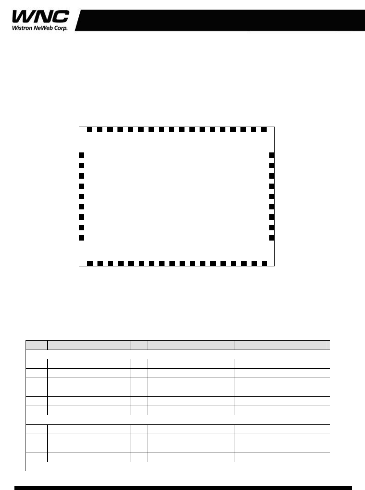
1.5ModulePinOut
Themoduleisdesignedas54pinsolderjointmoduleforSMTprocess.Thepin‐outisillustratedinthe
figure1‐2.
UART_TX
GND
GND
GND
UART_RX
S D_ DATA[2 ]
45
GND
GND
VCC_1V8
28
GND
GND
GND
GND
BT_ RF
WLAN_RF
BT_P CM_DIN
BT_P CM_ CLK
BT_P CM_ DO UT
BT_ PCM _SY NC
1
GND
VCC_VIO_X2
GND
JTAG_TCK
JTAG_TDI
JTAG_TRSTn
JTAG_ TMS _S YS
JTAG_TDO
18
S D_ DATA[3 ]
40 3035
S D_ DATA[0 ]
UART_RTS
S D_ DATA[1 ]
SD_ CMD
S D_CLK
VCC_3V3
VCC_3V3
VCC_3V0
VCC_VIO_X1
GND
GND
GND
27
VCC_3V3
VCC_3V3
VCC_WLAN_ ANT_DIAG
GND
WLAN_ANT_DIAG
25
20
19
51015
SLEEP _ CLK
ANT_SEL _P
RESETn
46
VCC_BT _ANT_DIAG
UART_CTS
BT _AN T_ D IAG
50
54
JTAG_TMS_CPU
NC
ANT_ SEL _N
Figure1‐2Pinoutof802.11b/g+Bluetoothmodule
Thepindefinitionisshowninthefollowingtable1‐2.
Pin#SignalNameI/OSignalDescriptionSignalCharacteristics
SDIOInterface
36SD_CLKI/OSDIOclock
37SD_CMDI/OSDIOcommandline
39SD_DAT_0I/OSDIOdatalinebit0
38SD_DAT_1I/OSDIOdatalinebit1
41SD_DAT_2I/OSDIOdatalinebit2
40SD_DAT_3I/OSDIOdatalinebit3
UARTInterface
45TXDOUARTserialdataoutput
44RXDIUARTserialdatainput
46CTSIUARTCleartosendsignal
43RTSOUARTReadytosendsignal
WLANandBluetoothRFInterface

The information contained herein is the exclusive property of WNC and shall not be distributed, reproduced, or disclosed in whole or in part without prior written permission of WNC. 8 / 30
W
LAN/BT System Integration Manual
17WLAN_RFI/OWLANantennain/out
2BT_RFI/OBluetoothantennain/out
AudioInterface–PCM/I2S
5BT_PCM_CLK/I2S_BCLKI/OPCMclock/I2Saudiobit
clock
7BT_PCM_SYNC/I2S_LRCL
K
I/OPCMsyncpulse/I2S
left/rightclock
4BT_PCM_DIN/I2S_DINIPCMdatainput/I2Sdata
input(forrecording)
6BT_PCM_DOUT/I2S_DO
UT
OPCMdataoutput/I2S
dataoutput(forplayback)
Control&PowerInterface
52RESET#IResetsignalActivelow
47SLEEP_CLKISleepclock
Coexistence
48ANT_SEL_PODifferentialAntennaSelect
Positiveoutput
49JTAG_TMS_CPUIJTAGTestModeSelect
(SelectstheinternalCPU
JTAGcontroller)
50NC
51ANT_SEL_PODifferentialAntennaSelect
Negativeoutput
AntennaDiagnosis
53VCC_BT_ANT_DIAGIExternalpowerforBT
antenna
diagnosis
54BT_ANT_DIAGOBTantennadiagnosis
output
20VCC_WLAN_ANT_DIAGIExternalpowerforWLAN
antennadiagnosis
19WLAN_ANT_DIAGOWLANantennadiagnosis
output
JointTestActionGroup(JTAG)andTestInterface
11JTAG_TCKIJTAGTsetClock
12JTAG_TDIIJTAGTsetDataInput
13JTAG_TDOOJTAGTestDataOutput
14JTAG_TRSTnIJTAGTestResetActivelow
15JTAG_TMS_SYSIJTAGTestModeSelect
(SelectstheSystemJTAG
controller)
Power&Ground
23,
24,
32,
33,
VCC_3V3PI3.3Vpowerinput3.3V+/‐1.5Visrequired.
29VCC_3V0PO3.0Vmonitoringoutput

The information contained herein is the exclusive property of WNC and shall not be distributed, reproduced, or disclosed in whole or in part without prior written permission of WNC. 9 / 30
W
LAN/BT System Integration Manual
34VCC_1V8PO1.8Vmonitoringoutput
26VCC_VIO_X1PI1.8/3.3VHostInterface
Supply
ForSDIO,UARTinterface
9VCC_VIO_X2PI3.3VDigitalInterface
supply
ForPCMinterface
1,3,
8,
10,
16,
18,
21,
22,
25,
27,
28,
30,
31,
35,
42
GNDPGround
Table1‐2PinOutDefinition
1.6Powermanagement
Modulesupply(VCC_3V3)
802.11b/g+BluetoothmodulesmustbesuppliedthroughVCC_3V3pinbyaDCpowersupply.Voltages
mustbestable,duetothesurgingconsumptionprofileoftheWiFi/BTsystem.
NameDescriptionRemarks
VCC_3V3ModuleSupplyCleanandstablesupplyisrequired:lowrippleandlow
voltagedropmustbeguaranteed.Voltageprovidedhasto
bealwaysabovetheminimumlimitoftheoperatingrange.
ConsiderthattherearelargecurrentspikeinWIFIorBT
connectedmode.
VCC_IO_X1,
VCC_IO_X2
I/OSupplyCleanandstablesupplyisrequired:lowrippleandlow
voltagedropmustbeguaranteed.Voltageprovidedhasto
bealwaysabovetheminimumlimitoftheoperatingrange.
GNDGroundGNDpinsareinternallyconnectedbutgood(low
impedance)externalgroundcanimproveRF
performances.AllGNDpinsmustbeexternallyconnected
toground.
The information contained herein is the exclusive property of WNC and shall not be distributed, reproduced, or disclosed in whole or in part without prior written permission of WNC. 10 / 30
W
LAN/BT System Integration Manual
Operatingcondition
SymbolParameterConditionMinTypMaxUnits
VCC_3V3Modulepowersupply2.973.33.63V
1.621.81.98VVIO_X1HostinterfacedigitalI/O
powersupply2.973.33.63V
VIO_X2DigitalI/Opowersupply 2.973.33.63V
VCC_3V01.8Vinternalvoltagesupply 2.93.03.1V
VCC_1V81.8Vinternalvoltagesupply 1.71.81.9V
TAAmbientoperatingtemperature ‐40 85℃
TJMaximumjunctiontemperature 125℃
1.7RFconnection
TheRFpinhas50Ωnominalimpedanceandmustbeconnectedtotheantennathrougha50Ω
transmissionlinetoallowtransmissionandreceptionofradiofrequency(RF)signalsintheWIFIandBT
operatingbands.
NameDescriptionRemarks
WLAN_RFWLANantennain/out50nominalimpedance.
BT_RFBluetoothantennain/out50nominalimpedance.
RFportESDratingis+/‐8kV(contactdischarge).Ahigherprotectionlevelcouldberequiredifthelineis
externallyaccessibleontheapplicationboard.Notethatantennadetectionfunctionalitywillbenot
providedimplementingforESDprotectionontheANTport.
Chooseanantennawithoptimalradiatingcharacteristicsforthebestelectricalperformanceandoverall
modulefunctionality.Aninternalantenna,integratedontheapplicationboard,oranexternalantenna,
connectedtotheapplicationboardthroughaproper50Ωconnector,canbeused.

The information contained herein is the exclusive property of WNC and shall not be distributed, reproduced, or disclosed in whole or in part without prior written permission of WNC. 11 / 30
W
LAN/BT System Integration Manual
2.Interfaces
ThischapterdescribestheinterfacesontheWLAN/BTmodules:SDIO,UART,PCM,JTAG,Antenna
diagnosis.
2.1SDIOInterface
ThemodulesupportsaSDIOdeviceinterfacethatconformstotheindustrystandardSDIOfullspeed
cardspecificationandallowsahostcontrollerusingtheSDIObusprotocoltoaccesstheWLAN
and/orBluetoothdevice.ThisdevicealsosupportshighspeedmodeasdefinedinSDIO1.2
specification.
TheSDIOinterfacesupportsdualfunctionoperations,forWLANandBluetooth.Dualfunctionality
allowstheuseofindependentclientdriversforWALNand/orBluetoothonthehostplatform.Since
thesefunctionssharethesamephysicalinterface,anarbitrationschemeisrequiredintheSDIObus
driveronthehostplatform.
TheSDIOinterfacesupportsSPI,1‐bitSDIO,4‐bitSDIOtransfermodesatthefullclockrangeof0to
50MHz.
2.1.1SDIOInterfaceSignalDescription
PinNameSignalNameTypeDescription
SD_CLKCLKI/OSDIO4‐bitmode:Clock
SDIO1‐bitmode:Clock
SDIOSPImode:Clock
SD_CMDCMDI/OSDIO4‐bitmode:Command/Response
SDIO1‐bitmode:Commandline
SDIOSPImode:Datain
SD_DAT_0DAT0I/OSDIO4‐bitmode:Datalinebit[0]
SDIO1‐bitmode:Dataline
SDIOSPImode:Dataout
SD_DAT_1DAT1I/OSDIO4‐bitmode:Datalinebit[1]
SDIO1‐bitmode:Interrupt
SDIOSPImode:Interrupt
SD_DAT_2DAT2I/OSDIO4‐bitmode:Datalinebit[2]
SDIO1‐bitmode:ReadWait(optional)
SDIOSPImode:Reserved
The information contained herein is the exclusive property of WNC and shall not be distributed, reproduced, or disclosed in whole or in part without prior written permission of WNC. 12 / 30
W
LAN/BT System Integration Manual
SD_DAT_3DAT3I/OSDIO4‐bitmode:Datalinebit[3]
SDIO1‐bitmode:Notused
SDIOSPImode:Chipselect(Negativetrue)
2.1.2SDIOConnection/Function
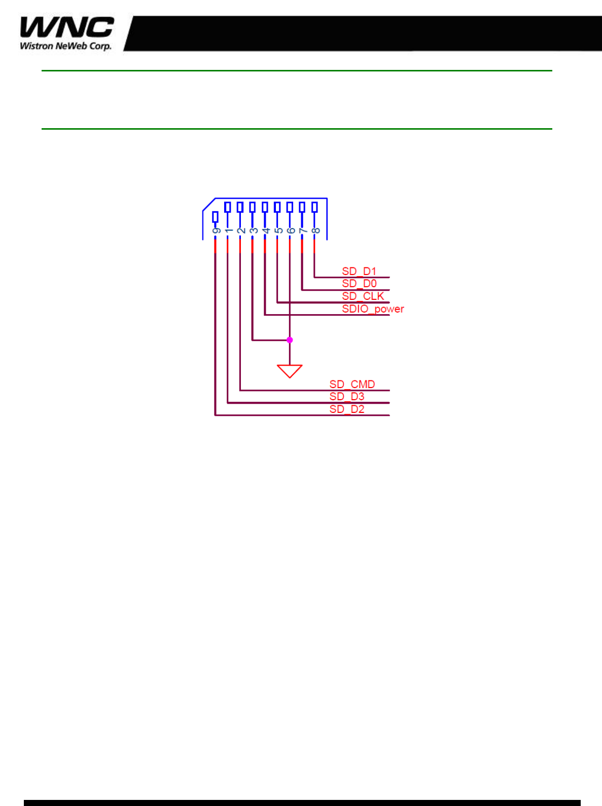
Figure1.1SDIOPhysicalConnection–4bitmode
Note:In4‐bitSDIOmode,dataistransferredonall4datapins(DAT[3:0]),andtheinterruptpinisnot
availableforexclusiveuseasitisutilizedasadatatransferline.Thus,iftheinterruptfunctionisrequired,
aspecialtimingisrequiredtoprovideinterrupts.The4‐bitSDIOmodeprovidesthehighestdatatransfer
possible,upto100Mbps.
2.2UARTInterface
ThemodulesupportsahighspeedUARTinterface,complianttotheindustrystandard16550
specification.Highspeedbaudratesaresupportedtoprovidethephysicaltransportbetweenthe
deviceandthehostforexchangingBluetoothdata.
2.2.1SignalBehavior
TXD
Serialdataoutputtotheperipheraldevice.
RXD
Serialdatainputfromtoperipheraldevice.

The information contained herein is the exclusive property of WNC and shall not be distributed, reproduced, or disclosed in whole or in part without prior written permission of WNC. 13 / 30
W
LAN/BT System Integration Manual
CTS
Clear‐to‐Sendinputfromtheperipheraldevice.
RTS
Request‐to‐Sendoutputtotheperipheraldevice.
2.3DigitalAudioInterface
DigitalaudiointerfacesincludePCMforvoiceapplicationandI2Sfordigitalstereoapplications.PCM
andI2Sinterfacesharethesamepins.
Voiceinterfacesupports.
HardwaresupportforcontinualtransmissionandreceptionofPCMdatawithoutprocessor
overhead.
StandardPCMclockratesfrom64KHzto2.048MHzwithmulti‐slothandshakeandsynchronization.
PCMencoding/decodingsupportofA‐law,μ‐law,andlinearvoice.
Stereoaudiointerfacesupports.
StandardrecordandplaybackforI2S,left‐justified,andright‐justifiedserialinterfaces.
PlaybackinIEC60958CompatibleAudioCodecInterface.
MasterandslavemodeforI2S,MSB,andLSBaudiointerfaces.
SlavemodewithoptiontouseasynchronousinternalCLK.
SlavemodewithoptionalslowersynchronousCLKinputfromhosttosavepower.
2.3.1BT_PCM_SYNC/I2S_LRCLK
PCMmode:BT_PCM_SYNC,input/output(outputifPCMinitiator,inputifPCMtarget)
Stereoaudiomode:I2S_LRCLK
Mastermode:output
Slavemode:input
2.3.2BT_PCM_CLK/I2S_BCLK
PCMmode:BT_PCM_CLK,input/output(outputifPCMinitiator,inputifPCMtarget)
Stereoaudiomode:I2S_BCLK
Mastermode:output
Slavemode:input
2.3.3BT_PCM_DOUT/I2S_DOUT
PCMmode:BT_PCM_DOUT,output
Stereoaudiomode:I2S_DOUT,output
2.3.4BT_PCM_DIN/I2S_DIN
PCMmode:BT_PCM_DIN,input

The information contained herein is the exclusive property of WNC and shall not be distributed, reproduced, or disclosed in whole or in part without prior written permission of WNC. 14 / 30
W
LAN/BT System Integration Manual
Stereoaudiomode:I2S_DIN,input
2.4RESET#
Resetsignal,activelow.ThemoduleisresetandthemodulebeginsthebootsequencewhenRESET#
inputpintransitionsfromlowtohigh.
2.5SLEEP_CLK
SLEEP_CLK,clockinputforexternalsleepclock.ThesleepclockisusedbythePMUduringpower
savemodes.
2.6JointTestActionGroup(JTAG)andTestInterface
JTAGisreservedforSWdebugandfailureanalysis.
JTAGInterfaceSignalDescription
PinNameTypeDescription
TCKIJTAGTestClockInput
TDIIJTAGTestDataInput
TDOOJTAGTestDataOutput
TRSTnI/OJTAGTestReset(activelow)
TMS_CPUIJTAGTestModeSelect
SelectstheinternalCPUJTAGcontroller
TMS_SYSIJTAGTestModeSelect
SelectstheSystemJTAGcontroller

The information contained herein is the exclusive property of WNC and shall not be distributed, reproduced, or disclosed in whole or in part without prior written permission of WNC. 15 / 30
W
LAN/BT System Integration Manual
2.7AntennaDiagnosis
Ifanexternalantennaequippeda50KohmfromitsRFcablecoretoGND,thenthisantenna
diagnosiscancheckwhethertheantennaispluggedwellornot.
2.7.1VCC_BT_ANT_DIAGandBT_ANT_DIAG
Ifanexternalantennaequippeda50KohmfromitsRFcablecoretoGNDandavoltageV1isapplied
toVCC_BT_ANT_DIAG,thenBT_ANT_DIAGcanbereadasV1/2 iftheconnectionofantennaandmodule
isgood.
2.7.2VCC_WLAN_ANT_DIAGandWLAN_ANT_DIAG
Ifanexternalantennaequippeda50KohmfromitsRFcablecoretoGNDandavoltageV2isapplied
toVCC_WLAN_ANT_DIAG,thenWLAN_ANT_DIAGcanbereadasV2/2 iftheconnectionofantennaand
moduleisgood.

The information contained herein is the exclusive property of WNC and shall not be distributed, reproduced, or disclosed in whole or in part without prior written permission of WNC. 16 / 30
W
LAN/BT System Integration Manual
3.Design‐In
3.1Design‐inchecklist
Thissectionprovidesadesign‐inchecklist.
3.1.1Schematicchecklist
Thefollowingarethemostimportantpointsforasimpleschematiccheck:
□ DCsupplymustprovideanominalvoltage(3.3V)atVCC_3V3pinsabovetheminimumnormal
operatingrangelimit.
□ DCsupplymustprovideanominalvoltage(3.3V)atVCC_VIO_X2pinsabovetheminimumnormal
operatingrangelimit.
□ DCsupplymustprovideanominalvoltage(3.3Vor1.8V)atVCC_VIO_X1pinsabovetheminimum
normaloperatingrangelimit.
□ DCsupplymustbecapabletoprovide0.5Acurrentburstswithmaximum200mVvoltagedropat
VCC_3V3pins.
□ DCsupplymustbecapabletoprovide0.1Acurrentburstswithmaximum200mVvoltagedropat
VCC_VIO_X2pins.
□ DCsupplymustbecapabletoprovide0.1Acurrentburstswithmaximum100mVvoltagedropat
VCC_VIO_X1pins.
□ VCC_3V3supplyshouldbeclean,withverylowripple/noise(lessthan200mVpp):suggestedpassive
filteringpartscanbeinserted.
□ VCC_VIO_X1supplyshouldbeclean,withverylowripple/noise(lessthan100mVpp):suggested
passivefilteringpartscanbeinserted.
□ VCC_VIO_X2supplyshouldbeclean,withverylowripple/noise(lessthan200mVpp):suggested
passivefilteringpartscanbeinserted.
□ ConnectonlyoneDCsupplytoVCC_3V3:differentDCsupplysystemsaremutuallyexclusive.
□ Checkthatvoltagelevelofanyconnectedpindoesnotexceedtherelativeoperatingrange.
□ CheckUARTsignalsdirection.
□ Checkthedigitalaudiointerfacespecificationstoconnectaproperdevice.
□ Toavoidanincreaseofmodulecurrentconsumptioninpowerdownmode,anyexternalsignals
connectedtothemoduledigitalpins(UART,PCM,SDIOinterface)mustbesetlowortri‐statedwhen
themoduleisinpowerdownmode.
□ Anyexternalsignalconnectedtothedigitalaudiointerfacemustbetri‐statedwhenthemoduleisin
powerdownmodeandmustbetri‐statedduringthemodulepower‐onsequence(atleastfor1500
msafterthestart‐upevent).
□ ProvideproperprecautionsforESDimmunityasrequiredontheapplicationboard.
□ Allthenotusedpinscanbeleftfloatingontheapplicationboard.
The information contained herein is the exclusive property of WNC and shall not be distributed, reproduced, or disclosed in whole or in part without prior written permission of WNC. 17 / 30
W
LAN/BT System Integration Manual
3.1.2Layoutchecklist
Thefollowingarethemostimportantpointsforasimplelayoutcheck:
□ Check50ΩimpedanceofANTline(WLAN_RF,BT_RF).
□ Followtherecommendationsoftheantennaproducerforcorrectantennainstallationand
deployment.
□ Ensurenocouplingoccurswithothernoisyorsensitivesignals.
□ VCCline(VCC_3V3,VCC_VIO_X1,VCC_VIO_X2)shouldbewideandshort.
□ RouteVCCsupplylineawayfromsensitiveanalogsignals.
□ Ensurepropergrounding.
□ OptimizeplacementforminimumlengthofRFlineandcloserpathfromDCsourceforVCC.
3.2DesignGuidelinesforLayout
ThefollowingdesignguidelinesmustbemetforoptimalintegrationofWLAN+BTmodulesonthefinal
applicationboard.
3.2.1Layoutguidelinesperpinfunction
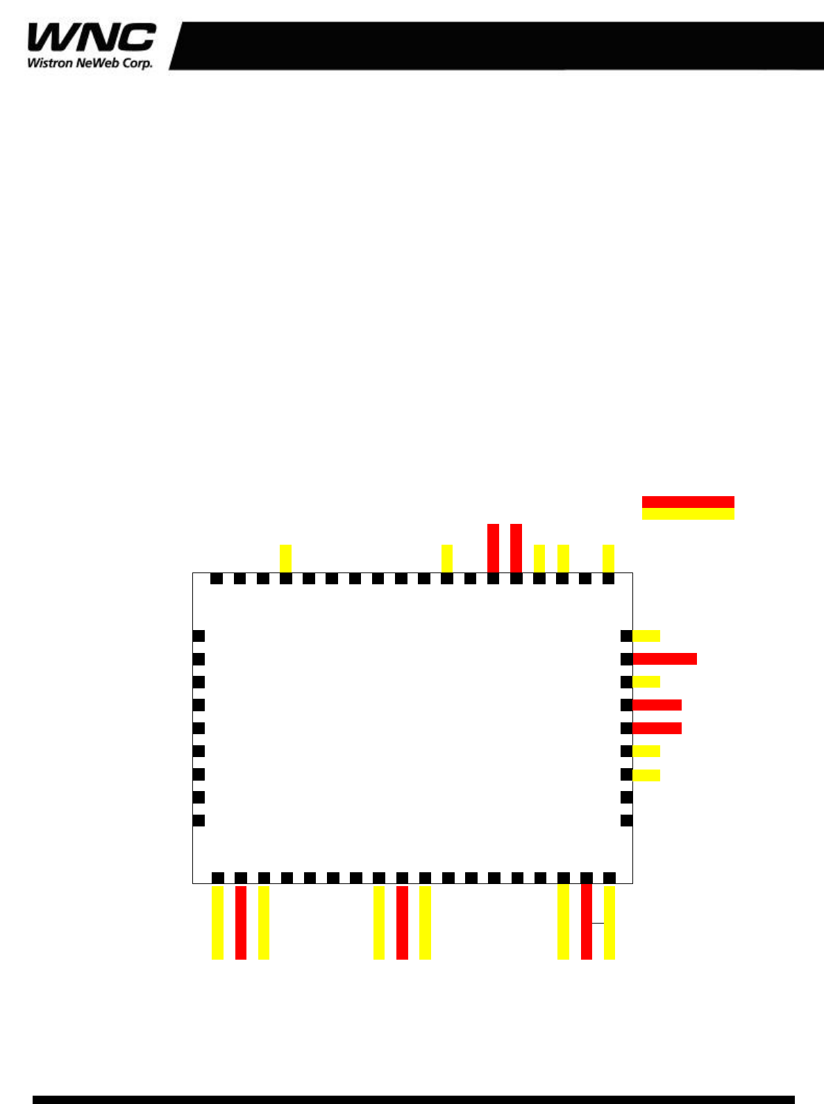
Thissectiongroupsthemodulepinsbysignalfunctionandprovidesarankingofimportancein
layoutdesign.
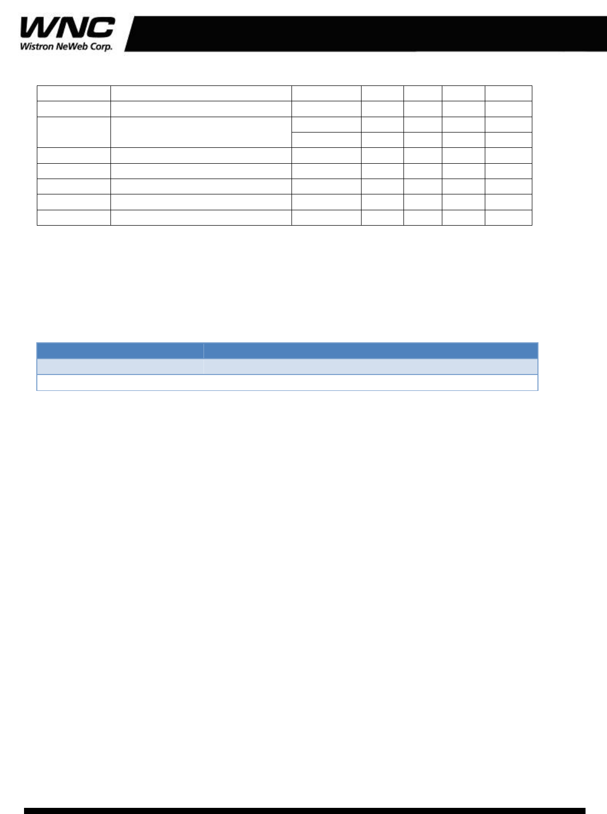
UART_TX
GND
GND
GND
UART_RX
S D_ DATA[2 ]
45
GND
GND
VCC_1V8
28
GND
GND
GND
GND
BT_ RF
WLAN_RF
BT_P CM_ DI N
BT_ PCM_ CLK
BT_P CM_ DO UT
BT_PCM_SY NC
1
GND
VCC_VIO_X2
GND
JTAG_TCK
JTAG_TDI
JTAG_TRSTn
JTAG _TM S_S YS
JTAG_TDO
18
S D_ DATA[3 ]
40 3035
S D_ DATA[0 ]
UART_RTS
SD_DATA[1]
SD_CMD
SD_CLK
VCC_3V3
VCC_3V3
VCC_3V0
VCC_VIO_X1
GND
GND
GND
27
VCC_3V3
VCC_3V3
VCC_WLAN_ANT_DIAG
GND
WLAN_ANT_DIAG
25
20
19
51015
SLEEP _ CLK
ANT_SEL _P
RESETn
46
VCC_BT_ANT_DIAG
UART_CTS
BT _ANT _ DIAG
50
54
JTAG_TMS_CPU
NC
ANT_ SEL _N
Very Important
Careful Layout
Common Practice
Legend :
Figure3‐1:Modulepin‐outwithhighlightedfunctions
The information contained herein is the exclusive property of WNC and shall not be distributed, reproduced, or disclosed in whole or in part without prior written permission of WNC. 18 / 30
W
LAN/BT System Integration Manual
Rank Function Pin(s) Layout Remarks
1st RFin/out BT_RF
WLAN_RF
Very
Important
Designfor50ohmcharacteristic
impedance
2nd DCSupply
VCC_3V3
VCC_VIO_X1
VCC_VIO_X2
Very
Important
VCClinesshouldbeshortandwide.
Routeawayfromsensitiveanalog
signals.
3rd Ground GND Careful
Layout providepropergrounding.
DigitalPins:
SDIO
interface
SD_CLK,SD_CMD,
SD_DAT_0,SD_DAT_1,
SD_DAT_2,SD_DAT_3
UART TXD,RXD,CTS,RTS
Digital
Audio
BT_PCM_DIN,
BT_PCM_SYNC,
BT_PCM_CLK,
BT_PCM_DOUT
RESET RESET#
SleepClock SLEEP_CLK
Antenna
Detection
VCC_BT_ANT_DIAG,
BT_ANT_DIAG,
VCC_WLAN_ANT_DIAG,
WLAN_ANT_DIAG
Antenna
Select
ANT_SEL_P,ANT_SEL_N
JTAG JTAG_TCK,JTAG_TDI,
JTAG_TDO,
JTAG_TRSTn,
JTAG_TMS_SYS,
JTAG_TMS_CPU
4th Common
Practice
Followcommonpracticerulesfor
digitalpinrouting.
Table3‐1:Pinlistinorderofdecreasingimportanceforlayoutdesign
3.2.1.1RFI/Oconnection
TheRFantennaconnectionpinBT_RF&WLAN_RFareverycriticalinlayoutdesign.ThePCBline
mustbedesignedtoprovide50Ωcharacteristicimpedanceandminimumlossuptoradiatingelement.
ProvidepropertransitionbetweentheBT_RF&WLAN_RFpadstoapplicationboardPCB.
IncreaseGNDkeep‐out(i.e.clearance)forBT_RF&WLAN_RFpinstoatleast250μmupto
adjacentpadsmetaldefinitionandupto250μmontheareabelowtheDataModule,asdescribed
inFigureXXX.
Thetransmissionlineuptoantennaconnectororpadmaybeamicrostriporastripline.Inany

The information contained herein is the exclusive property of WNC and shall not be distributed, reproduced, or disclosed in whole or in part without prior written permission of WNC. 19 / 30
W
LAN/BT System Integration Manual
casemustbedesignedtoachieve50Ωcharacteristicimpedance.
Microstriplinesareusuallyeasiertoimplementandthereducednumberoflayertransitionsupto
antennaconnectorsimplifiesthedesignanddiminishesreflectionlosses.However,the
electromagneticfieldextendstothefreeairinterfaceabovethestriplineandmayinteractwith
othercircuitry.
Buriedstriplineexhibitsbettershieldingtoincomingandgeneratedinterferences.Thereforeare
preferredforsensitiveapplication.Incaseastriplineisimplemented,carefullycheckthatthevia
pad‐stackdoesnotcouplewithothersignalsonthecrossedandadjacentlayers.
Minimizethetransmissionlinelength;theinsertionlossshouldbeminimizedasmuchaspossible,
intheorderofafewtenthsofadB.
ThetransmissionlineshouldnothaveabruptchangetothicknessandspacingtoGND,butmustbe
uniformandroutedassmoothlyaspossible.
ThetransmissionlinemustberoutedinasectionofthePCBwhereminimalinterferencefrom
noisesourcescanbeexpected.
RouteANTlinefarfromothersensitivecircuitsasitisasourceofelectromagneticinterference.
AvoidcouplingwithVCCroutingandanalogaudiolines.
EnsuresolidmetalconnectionoftheadjacentmetallayeronthePCBstack‐uptomainground
layer.
AddGNDviasaroundtransmissionline.
Ensurenoothersignalsareroutedparalleltotransmissionline,orthatothersignalscrosson
adjacentmetallayerIfthedistancebetweenthetransmissionlineandtheadjacentGNDarea(on
thesamelayer)doesnotexceed5timesthetracewidthofthemicrostrip,usethe“Coplanar
Waveguide”modelfor50Ωcharacteristicimpedancecalculation.
Don’troutemicrostriplinebelowdiscretecomponentorothermechanicsplacedontoplayer.
Whenterminatingtransmissionlineonantennaconnector(orantennapad)itisveryimportantto
strictlyfollowtheconnectormanufacturer’srecommendedlayout.
GNDlayerunderRFconnectorsandclosetoburiedviasshouldbecutoutinordertoremovestray
capacitanceandthuskeeptheRFline50Ω.Inmostcasesthelargeactivepadoftheintegrated
antennaorantennaconnectorneedstohaveaGNDkeep‐out(i.e.clearance)atleastonfirstinner
layertoreduceparasiticcapacitancetoground.Notethatthelayoutrecommendationisnot
alwaysavailablefromconnectormanufacturer:e.g.theclassicalSMAPin‐Through‐Holeneedsto
haveGNDclearedonallthelayersaroundthecentralpinuptoannularpadsofthefourGNDposts.
Check50ΩimpedanceofANTline.
3.2.1.2MainDCsupplyconnection
TheDCsupplyofWLAN/BTmodulesisveryimportantfortheoverallperformanceandfunctionality
oftheintegratedproduct.
VCCconnectionmaycarryamaximumburstcurrentintheorderof0.5A.Therefore,itistypically
implementedasawidePCBlinewithshortroutingfromDCsupply(DC‐DCregulator,batterypack,
etc)
EachvoltagedropintheDCsupplytrackwillrestricttheoperatingmarginatthemainDCsource
output.Therefore,thePCBconnectionhastoexhibitaminimumorzerovoltagedrop.Avoidany
seriescomponentwithEquivalentSeriesResistance(ESR)greaterthanafewmΩ.
Giventhelargeburstcurrent,VCClineisasourceofdisturbanceforothersignals.Thereforeroute
VCCthroughaPCBareaseparatedfromsensitiveanalogsignals.Typicallyitisgoodpracticeto
interposeatleastonelayerofPCBgroundbetweenVCCtrackandothersignalrouting.
TheVCCsupplycurrentsupplyflowsbacktomainDCsourcethroughGNDasgroundcurrent:
provideadequatereturnpathwithsuitableuninterruptedgroundplanetomainDCsource.

The information contained herein is the exclusive property of WNC and shall not be distributed, reproduced, or disclosed in whole or in part without prior written permission of WNC. 20 / 30
W
LAN/BT System Integration Manual
AtankcapacitorwithlowESRisoftenusedtosmoothcurrentspikes.Thisismosteffectivewhen
placedascloseaspossibletoVCC.FrommainDCsource,firstconnectthecapacitorandthenVCC.
IfthemainDCsourceisaswitchingDC‐DCconverter,placethelargecapacitorclosetotheDC‐DC
outputandminimizetheVCCtracklength.OtherwiseconsiderusingseparatecapacitorsforDC‐DC
converterandWLAN/BTmoduletankcapacitor.
VCC_3V3isdirectlyconnectedtotheRFpoweramplifier.AddcapacitorinthepFrangefromVCC
toGNDalongthesupplypath.
SinceVCC_3V3isdirectlyconnectedtoRFPowerAmplifier,voltagerippleathighfrequencymay
resultinunwantedspuriousmodulationoftransmitterRFsignal.Thisisespeciallyseenwith
switchingDC‐DCconverters,inwhichcaseitisbettertoselectthehighestoperatingfrequencyfor
theswitcherandaddalargeL‐CfilterbeforeconnectingtoWLAN/BTmoduleintheworstcase.
ThelargecurrentgeneratesamagneticfieldthatisnotwellisolatedbyPCBgroundlayersand
whichmayinteractwithotheranalogmodules(e.g.VCO)evenifplacedonoppositesideofPCB.In
thiscaserouteVCCawayfromothersensitivefunctionalunits.
IfVCCisprotectedbytransientvoltagesuppressor/reversepolarityprotectiondiodetoensure
thatthevoltagemaximumratingsarenotexceeded,placetheprotectingdevicealongthepath
fromtheDCsourcetowardWLAN/BTmodule,preferablyclosertotheDCsource(otherwise
functionalitymaybecompromised).
3.2.1.3Modulegrounding
GoodconnectionofthemodulewithapplicationboardsolidgroundlayerisrequiredforcorrectRF
performance.ItsignificantlyreducesEMCissues.
ConnecteachGNDpinwithapplicationboardsolidGNDlayer.Itisstronglyrecommendedthat
eachGNDpadsurroundingVCCandANTpinshaveoneormorededicatedviadowntoapplication
boardsolidgroundlayer.
IftheapplicationboardisamultilayerPCB,thenitisrequiredtotighttogethereachGNDareawith
completeviastackdowntomainboardgroundlayer.
Itisrecommendedtoimplementonelayeroftheapplicationboardasgroundplane.
GoodgroundingofGNDpadswillalsoensurethermalheatsink.
3.2.1.4Digitalpins
ExternalReset(RESET#):inputforexternalreset,alogiclowvoltagewillresetthemodule.RESET#
havetobeassertedbeforeVCCispoweredON,andthede‐assertionofRESET#needsatleast1ms
delayafterVCCispoweredandstable.
SDIO(SD_CLK,SD_CMD,SD_DAT_0,SD_DAT_1,SD_DAT_2,SD_DAT_3):theSDIOlayoutmaybe
criticaliftheapplicationprocessorisplacedfarawayfromWLAN/BTmoduleorinclosevicinityof
RFantenna.Inthefirstcasethelongconnectionmayradiatehigherharmonicofdigitaldata.Inthe
secondcasethesameharmonicsmaybepickedupandcreateself‐interferencethatcanreducethe
sensitivityofWLAN/BTReceiverchannelswhosecarrierfrequencyiscoincidentwithharmonic
frequencies.InthelatercaseusingRFbypasscapacitorsonthedigitallinewillmitigatethe
problem.
DigitalAudio(BT_PCM_CLK,BT_PCM_SYNC,BT_PCM_DIN,BT_PCM_DOUT):thePCMinterface
requiresthesameconsiderationregardingelectro‐magneticinterferenceastheSDIO.Keepthe
tracesshortandavoidcouplingwithRFlineorsensitiveanaloginputs.
UART(TXD,RXD,CTS,RTS):theserialinterfacerequirethesameconsiderationregarding
electro‐magneticinterferenceasforSDIO.KeepthetracesshortandavoidcouplingwithRFlineor
sensitiveanaloginputs.
JTAG(JTAG_TCK,JTAG_TDI,JTAG_TDO,JTAG_TRSTn,JTAG_TMS_SYS,JTAG_TMS_CPU):thedebug
The information contained herein is the exclusive property of WNC and shall not be distributed, reproduced, or disclosed in whole or in part without prior written permission of WNC. 21 / 30
W
LAN/BT System Integration Manual
interfacerequirethesameconsiderationregardingelectro‐magneticinterferenceasforSDIO.Keep
thetracesshortandavoidcouplingwithRFlineorsensitiveanaloginputs.
3.2.2Footprintandpastemask
Figure3‐2andFigure3‐3describethefootprintandproviderecommendationsforthestencilfor
WLAN/BTmodules.Thesearerecommendationsonlyandnotspecifications.
Figure3‐2:WLAN/BTmodulespaddesign
Figure3‐3:WLAN/BTmodulesstencildesign
Thepastemaskoutlineneedstobeconsideredwhendefiningtheminimaldistancetothenext
component.
Theexactgeometry,distances,stencilthicknessesandsolderpastevolumesmustbeadaptedto
thespecificproductionprocesses(e.g.solderingetc.)ofthecustomer.
The information contained herein is the exclusive property of WNC and shall not be distributed, reproduced, or disclosed in whole or in part without prior written permission of WNC. 22 / 30
W
LAN/BT System Integration Manual
3.2.3Placement
OptimizeplacementforminimumlengthofRFlineandcloserpathfromDCsourceforVCC.
3.3Modulethermalconsideration
Thetemperatureincreaseofthemainchip88w8688,PALX5511andLDOMAX4835onaWLAN/BT
modulemountedona168x46.45x1.3mmFR4PCBwithahighcoverageofcopper(e.g.theEVK‐G25H
evaluationkit)instillairconditionsarelessthan28 ,25 ,25 respectively.℃℃℃ Thisisbasedonaworse
casewithfullcontinuousWLANTXmode.
Thistemperatureincreasewillbedifferentthantheoneprovidedifthemoduleismountedona
PCBwithdifferentsizeandcharacteristics.
3.4Antennaguidelines
Antennacharacteristicsareessentialforgoodfunctionalityofthemodule.Theradiating
performanceofantennashasdirectimpactonthereliabilityofconnectionovertheAirInterface.Bad
terminationofANTcanresultinpoorperformanceofthemodule.
Thefollowingparametersshouldbechecked:ItemRecommendations
Item Recommendations
Impedance 50Ωnominalcharacteristicimpedance
Frequency WIFI:2400MHz~2483.5MHz
BT:2400MHz~2483.5MHz
V.S.W.R <2:1recommended
ReturnLoss S
11
<‐10dBrecommended,S
11
<‐8dBacceptable
Gain <3dBi
Table3‐2:Generalrecommendationforantenna
Antennasaretypicallyavailableas:
Linearmonopole:typicalforfixedapplication.Theantennaextendsmostlyasalinearelementwith
adimensioncomparabletolambda/4ofthelowestfrequencyoftheoperatingband.Magnetic
basemaybeavailable.CableordirectRFconnectorsarecommonoptions.Theintegration
normallyrequiresthefulfillmentofsomeminimumguidelinessuggestedbyantennamanufacturer.
Patch‐likeantenna:bettersuitedforintegrationincompactdesigns.Theyaremostlycustom
designswheretheexactdefinitionofthePCBandproductmechanicaldesignisfundamentalfor
tuningofantennacharacteristics.
Forintegrationobservetheserecommendations:
Ensure50Ωantennatermination,minimizetheV.S.W.R.orreturnloss,asthiswilloptimizethe
electricalperformanceofthemodule.
Selectantennawithbestradiatingperformance.
Ifacableisusedtoconnecttheantennaradiatingelementtoapplicationboard,selectashort
cablewithminimuminsertionloss.Thehighertheadditionalinsertionlossduetolowqualityor
longcable,thelowertheconnectivity.
Followtherecommendationsoftheantennamanufacturerforcorrectinstallationanddeployment.
Donotincludeantennawithinclosedmetalcase.
Donotplaceantennainclosevicinitytoendusersincetheemittedradiationinhumantissueis
limitedbyS.A.R.regulatoryrequirements.
Donotusedirectivityantennasincetheelectromagneticfieldradiationintensityislimitedinsome
countries.
Takecareofinteractionbetweenco‐locatedRFsystemssincetheWIFI/BTtransmittedpowermay
interactordisturbtheperformanceofcompanionsystems.

The information contained herein is the exclusive property of WNC and shall not be distributed, reproduced, or disclosed in whole or in part without prior written permission of WNC. 23 / 30
W
LAN/BT System Integration Manual
Placeantennafarfromsensitiveanalogsystemsoremploycountermeasurestoreduce
electromagneticcompatibilityissuesthatmayarise.
3.4.1Antennatermination
WLAN/BTmodulesaredesignedtoworkona50Ωload.However,realantennashavenoperfect
50Ωloadonallthesupportedfrequencybands.Toreduceasmuchaspossibleperformance
degradationduetoantennamismatch,thefollowingrequirementsshouldbemet:
Measuretheantennaterminationwithanetworkanalyzer:connecttheantennathroughacoaxial
cabletothemeasurementdevice,the|S11|indicateswhichportionofthepowerisdeliveredto
antennaandwhichportionisreflectedbytheantennabacktothemoduleoutput.
Agoodantennashouldhavea|S11|below‐10dBovertheentirefrequencyband.Dueto
miniaturization,mechanicalconstraintsandotherdesignissues,thisvaluewillnotbeachieved.A
valueof|S11|ofabout‐8dBisacceptable.
3.4.2Antennadiagnosisfunctionality
TheinternalantennadiagnosiscircuitisbasedonADCmeasurementatANT_DIAGpin:theRFport
isDCcoupledtotheADCunitintheapplicationprocessorwhichinjectsaDCvoltage(3.3V)on
VCC_ANT_DIAGandmeasurestheresultingDCvoltagetoevaluatetheresistancefromANTpadtoGND.
TheantennadetectionisperformedbythemeasurementoftheresistancefromANTpadtoGND.
Toachievegoodantennadetectionfunctionality,useanRFantennawithbuilt‐inresistorfromANT
signaltoGND,orimplementanequivalentsolutionwithacircuitbetweentheantennacableconnection
andtheradiatingelement.
PleasenotethattheDCimpedanceatRFportforsomeantennasmaybeaDCopen(e.g.linear
monopole)oraDCshorttoreferenceGND(e.g.PIFAantenna).Forthoseantennas,withoutthe
diagnosticcircuitFigure53,themeasuredDCresistancewillbealwaysontheextremeofmeasurement
range(respectivelyopenorshort),andtherewillbenomeantodistinguishfromdefectonantenna
pathwithsimilarcharacteristic(respectively:removaloflinearantennaorRFcableshortedtoGNDfor
PIFAantenna).
Furthermore,anyotherDCsignalinjectedtotheRFconnectionfromANTconnectortoradiating
elementwillalterthemeasurementandproduceinvalidresultsforantennadetection.
Itisrecommendedtouseanantennawithabuilt‐indiagnosticresistorof51kΩtoassuregood
antennadetectionfunctionalityandtoavoidareductionofmoduleRFperformances.

The information contained herein is the exclusive property of WNC and shall not be distributed, reproduced, or disclosed in whole or in part without prior written permission of WNC. 24 / 30
W
LAN/BT System Integration Manual
4.HandlingandSoldering
4.1Packaging,shipping,storageandmoisturepreconditioning
HandlingRequirements
DONOTTOUCHANYPINOFWIFIMODULEWHILEASSEMBLYING.
Moisturepreconditioning
ThisWLAN/BTmodulemeetsMSL3.PleasefollowJ‐STD‐033Btohandlethismodule.
4.2SolderingRequirements
4.2.1SolderingIronSoldering
SolderTemperature:350oC
ImmersionDuration:2~3seconds
4.2.2ReflowProfile
Aconvectiontype‐solderingovenisstronglyrecommendedovertheinfraredtyperadiationoven.
Convectionheatedovensallowprecisecontrolofthetemperatureandallpartswillbeheatedupevenly,
regardlessofmaterialproperties,thicknessofcomponentsandsurfacecolor.
Considerthe"IPC‐7530Guidelinesfortemperatureprofilingformasssoldering(reflowandwave)
processes.”
PreheatPhase
Initialheatingofcomponentleadsandballs.Residualhumiditywillbedriedout.Pleasenotethatthis
preheatphasewillnotreplacepriorbakingprocedures.
Temperatureriserate:max3°C/sIfthetemperatureriseistoorapidinthepreheatphaseitmaycause
excessiveslumping.
PreheatTime:60~120secIfthepreheatisinsufficient,ratherlargesolderballstendtobegenerated.
Conversely,ifperformedexcessively,fineballsandlargeballswillbegeneratedinclusters.
EndTemperature:140~190°CIfthetemperatureistoolow,non‐meltingtendstobecausedinareas
containinglargeheatcapacity.
Heating/ReflowPhase
Thetemperaturerisesabovetheliquidstemperatureof227°C.Avoidasuddenriseintemperatureasthe
slumpofthepastecouldbecomeworse.
Limittimeabove227°Cliquidstemperature:30~70sec
Peakreflowtemperature:235~250°C
CoolingPhase
Acontrolledcoolingavoidsnegativemetallurgicaleffects(solderbecomesmorebrittle)ofthesolderand
possiblemechanicaltensionsintheproducts.Controlledcoolinghelpstoachievebrightsolderfillets
withagoodshapeandlowcontactangle.
Temperaturefallrate:max4°C/s
The information contained herein is the exclusive property of WNC and shall not be distributed, reproduced, or disclosed in whole or in part without prior written permission of WNC. 25 / 30
W
LAN/BT System Integration Manual
4.2.3SolderingPaste
Useof"NoClean"solderingpasteisstronglyrecommended,asitdoesnotrequirecleaningafterthe
solderingprocesshastakenplace.Thepastelistedintheexamplebelowmeetsthesecriteria.
SolderingPaste:ACS‐SN100C‐MA1
Alloyspecification:Sn‐0.7Cu‐0.05Ni+Ge(99.2%Tin/0.7%Copper/0.05%Nickel/Germanium)
MeltingTemperature:227°C
StencilThickness:120μmforbaseboards
Thefinalchoiceofthesolderingpastedependsontheapprovedmanufacturingprocedures.
Thequalityofthesolderjointsontheconnectors(’halfvias’)shouldmeettheappropriateIPC
specification.
The information contained herein is the exclusive property of WNC and shall not be distributed, reproduced, or disclosed in whole or in part without prior written permission of WNC. 26 / 30
W
LAN/BT System Integration Manual
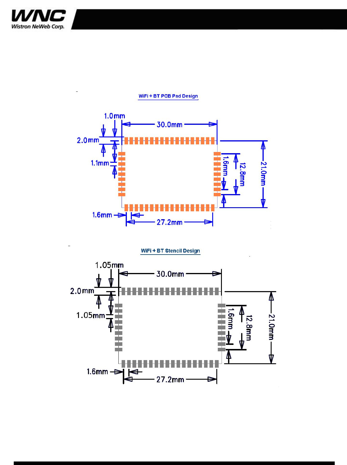
4.2.4PCBLayoutFootprintDesign
4.2.4.1ModuleDimensions
4.2.4.2PCBLayoutPadDesign
The information contained herein is the exclusive property of WNC and shall not be distributed, reproduced, or disclosed in whole or in part without prior written permission of WNC. 27 / 30
W
LAN/BT System Integration Manual
4.2.4.3StencilDesign
Stencilthickness:0.10mm~0.15mm.
Solderpastethickness:0.12mm~0.18mm

The information contained herein is the exclusive property of WNC and shall not be distributed, reproduced, or disclosed in whole or in part without prior written permission of WNC. 28 / 30
W
LAN/BT System Integration Manual
5ProductTesting
5.1Productiontest
WNCfocusesonhighqualityforitsproducts.Allunitsproducedarefullytested.Defectiveunitsare
analyzedindetailtoimprovetheproductionquality.
Thisisachievedwithautomatictestequipment,whichdeliversadetailedtestreportforeachunit.The
followingmeasurementsaredone:
Measurementofvoltagesandcurrents
MeasurementofRFcharacteristics
Testattemperature75℃for30minutes

The information contained herein is the exclusive property of WNC and shall not be distributed, reproduced, or disclosed in whole or in part without prior written permission of WNC. 29 / 30
W
LAN/BT System Integration Manual
FederalCommunicationCommissionInterferenceStatement
ThisequipmenthasbeentestedandfoundtocomplywiththelimitsforaClassBdigitaldevice,
pursuanttoPart15oftheFCCRules.Theselimitsaredesignedtoprovidereasonableprotectionagainst
harmfulinterferenceinaresidentialinstallation.Thisequipmentgenerates,usesandcanradiateradio
frequencyenergyand,ifnotinstalledandusedinaccordancewiththeinstructions,maycauseharmful
interferencetoradiocommunications.However,thereisnoguaranteethatinterferencewillnotoccur
inaparticularinstallation.Ifthisequipmentdoescauseharmfulinterferencetoradioortelevision
reception,whichcanbedeterminedbyturningtheequipmentoffandon,theuserisencouragedtotry
tocorrecttheinterferencebyoneofthefollowingmeasures:
●Reorientorrelocatethereceivingantenna.
●Increasetheseparationbetweentheequipmentandreceiver.
●Connecttheequipmentintoanoutletonacircuitdifferentfromthattowhichthereceiveris
connected.
●Consultthedealeroranexperiencedradio/TVtechnicianforhelp.
FCCCaution:Anychangesormodificationsnotexpresslyapprovedbythepartyresponsiblefor
compliancecouldvoidtheuser’sauthoritytooperatethisequipment.
ThisdevicecomplieswithPart15oftheFCCRules.Operationissubjecttothefollowingtwoconditions:
(1)Thisdevicemaynotcauseharmfulinterference,and(2)thisdevicemustacceptanyinterference
received,includinginterferencethatmaycauseundesiredoperation.
ForproductavailableintheUSA/Canadamarket,onlychannel1~11canbeoperated.Selectionofother
channelsisnotpossible.
Thisdeviceanditsantenna(s)mustnotbeco‐locatedoroperationinconjunctionwithanyother
antennaortransmitter.
FCCRadiationExposureStatement:
ThisequipmentcomplieswithFCCradiationexposurelimitssetforthforanuncontrolledenvironment.
Thisequipmentshouldbeinstalledandoperatedwithminimumdistance20cmbetweentheradiator&
yourbody.
IMPORTANT NOTE:
This module is intended for OEM integrator. The OEM integrator is still responsible for the FCC compliance
requirement of the end product, which integrates this module.
20cm minimum distance has to be able to be maintained between the antenna and the users for the host this module
is integrated into. Under such configuration, the FCC radiation exposure limits set forth for an population/uncontrolled
environment can be satisfied.
Any changes or modifications not expressly approved by the manufacturer could void the user's authority to operate
this equipment.
USERS MANUAL OF THE END PRODUCT:
In the users manual of the end product, the end user has to be informed to keep at least 20cm separation with the
antenna while this end product is installed and operated. The end user has to be informed that the FCC
radio-frequency exposure guidelines for an uncontrolled environment can be satisfied. The end user has to also be
informed that any changes or modifications not expressly approved by the manufacturer could void the user's

The information contained herein is the exclusive property of WNC and shall not be distributed, reproduced, or disclosed in whole or in part without prior written permission of WNC. 30 / 30
W
LAN/BT System Integration Manual
authority to operate this equipment. If the size of the end product is smaller than 8x10cm, then additional FCC part
15.19 statement is required to be available in the users manual: This device complies with Part 15 of FCC rules.
Operation is subject to the following two conditions: (1) this device may not cause harmful interference and (2) this
device must accept any interference received, including interference that may cause undesired operation.
LABEL OF THE END PRODUCT:
The final end product must be labeled in a visible area with the following " Contains TX FCC ID:
NKRUWMWBT-CWM01". If the size of the end product is larger than 8x10cm, then the following FCC part 15.19
statement has to also be available on the label: This device complies with Part 15 of FCC rules. Operation is
subject to the following two conditions: (1) this device may not cause harmful interference and (2) this device must
accept any interference received, including interference that may cause undesired operation.