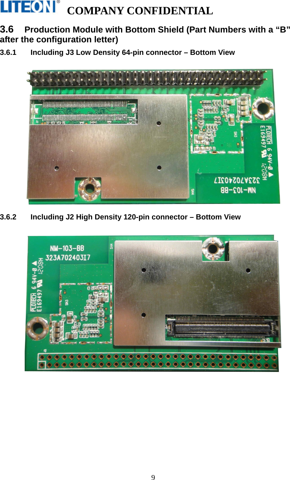
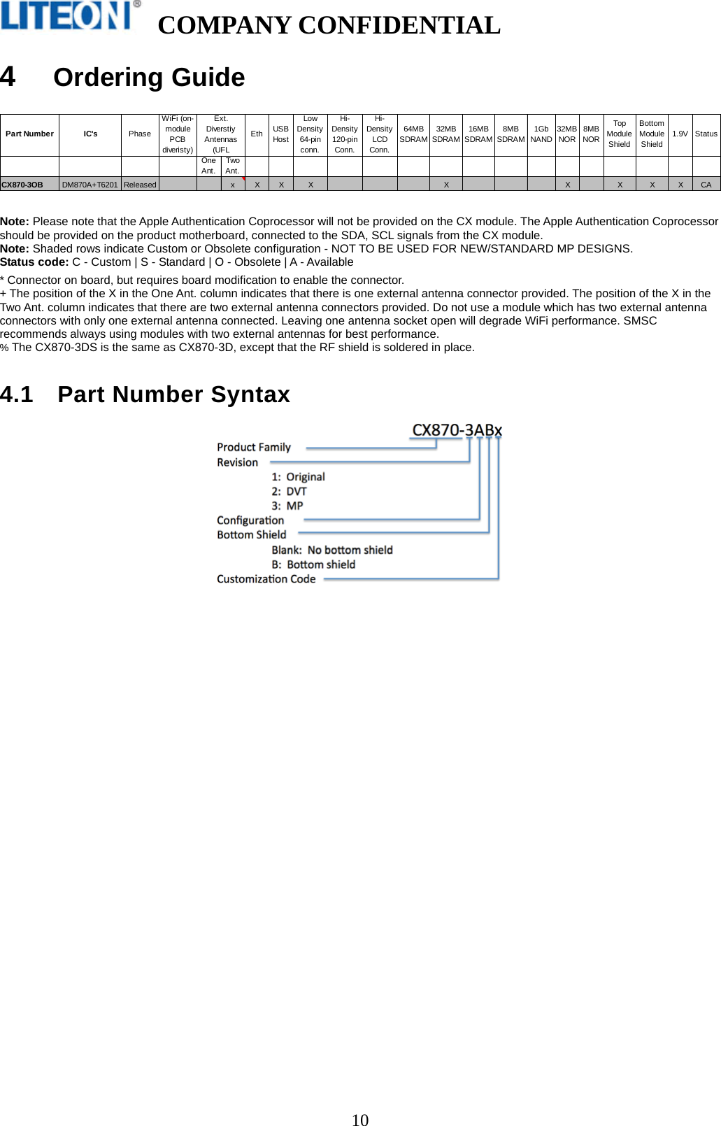
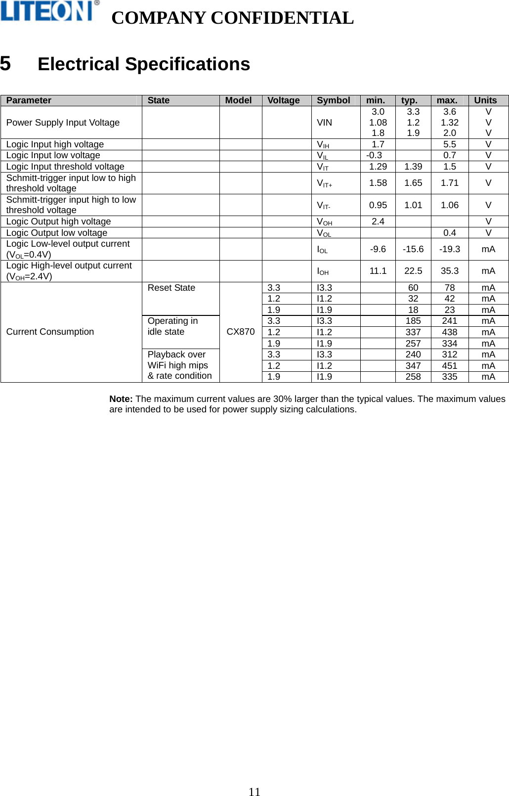
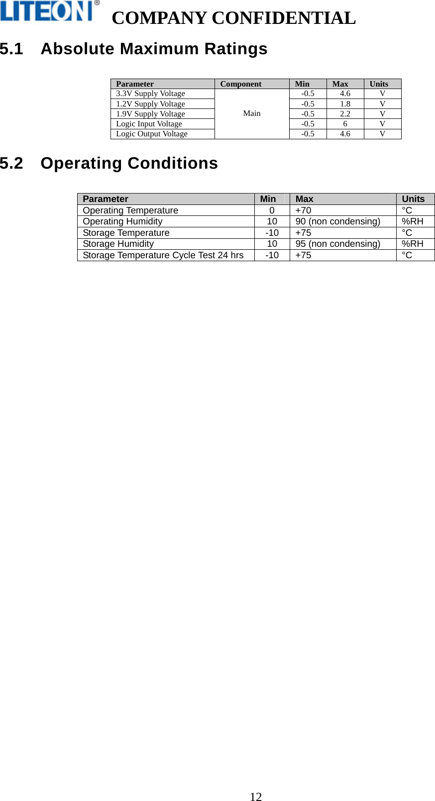
Yamaha VX77A CX870-3OB User Manual UserMan

Yamaha Corporation CX870-3OB UserMan

UserMan

  COMPANY CONFIDENTIAL    1        客 戶 名 稱: Customer Name:  YAMAHA          品    名 (Part Name)  SMSC CX870-3OB Module 承認書版本(Approval Sheet Rev.)  Preliminary version 客戶料號  (Customer Part No.)   光寶料號 (Liteon Part No.)    客  戶  簽  認 Customer Approval: _________________________________________  Prepared by  Reviewed by  Approved by Frank Gung      Total Pages  Date  Sales  2013/10/09 Elisa Liou 4F, 90, Chien 1 Road, Chungho, New Taipei City 235, Taiwan, R.O.C.TEL: +886-2-2222-6181   Fax: +886-2-2222-3882光寶科技股份有限公司台北縣中和市建一路 90 號4F電話: 02-2222-6181  傳真: 02-2222-3882承     認     書 (Specification Sheet)
  COMPANY CONFIDENTIAL    2IndexIndex.........................................................................................................................................................2Revision History.......................................................................................................................................3Part1. Module Spec Sheet....................................................................................................................41Introduction ....................................................................................................................................42Block Diagram ................................................................................................................................43Board Pictures.................................................................................................................................53.1Top View of CX Module........................................................................................................53.2Bottom View of CX Module..................................................................................................63.2.1CX Module Bottom View w/64-pin Low Density Connector.............................................63.2.2CX Module Bottom View w/120-pin Media Connector .....................................................63.3Production Module with Top and RF shields in place – Top View........................................73.4Production Module with 64-pin Connector Option – Side View...........................................73.5Example Production Module Showing Soldered RF Shield..................................................83.6Production Module with Bottom Shield (Part Numbers with a “B” after the configuration letter) 93.6.1Including J3 Low Density 64-pin connector – Bottom View..............................................93.6.2Including J2 High Density 120-pin connector – Bottom View...........................................94Ordering Guide.............................................................................................................................104.1Part Number Syntax.............................................................................................................105Electrical Specifications...............................................................................................................115.1Absolute Maximum Ratings.................................................................................................125.2Operating Conditions ...........................................................................................................125.3WiFi Specification (CX870 only) ........................................................................................136Regulatory Compliance and Quality ..........................................................................................146.0.1 Antenna Considerations.............................................................................................................146.0.2 CX Power Settings Used For Modular Approval......................................................................146.0.3 FCC IC Warning Message.........................................................................................................156.1RoHS....................................................................................................................................176.2Environmental Test...............................................................................................................176.3ESD and Transient Test (Applies to LAN and USB external connections only).................176.4Magnetic Field Test..............................................................................................................176.5MTBF...................................................................................................................................176.6Mechanical Specifications....................................................................................................176.7Module Quality ....................................................................................................................177Board Dimensions and Weight....................................................................................................187.1Top & Bottom View of CX870 Module without Bottom Shield .........................................187.1.1Top & Bottom View of CX Module with Bottom Shield..................................................187.2Side View of CX870 module without Bottom Shield..........................................................197.2.1Side View of CX Module with Bottom Shield except CX870-3JB ..................................197.33D View of CX870 Module without Bottom Shield............................................................207.4Module Weight.....................................................................................................................208Connectors and Connections.......................................................................................................218.1WLAN UFL Antenna Connector (optional).........................................................................218.2Module Connectors..............................................................................................................218.2.1Pin Descriptions ................................................................................................................228.2.2Connector PIN Assignments .............................................................................................278.2.3GPIO Assignments............................................................................................................299Application Guidelines.................................................................................................................309.1Power Supply sequencing and Reset Timing.......................................................................30
  COMPANY CONFIDENTIAL    39.1.1Power up, Reset and Power Down Timing .......................................................................319.2RF Considerations................................................................................................................31                        Revision History  Date Version Description 10/09/2013 Rev 00  Preliminary         This documentation describes the marketing requirements specification of the Lite-on made CX870 Wireless module. It is a confidential document of LITEON.
  COMPANY CONFIDENTIAL    4Part1. Module Spec Sheet 1  Introduction  The CX-series module is a single-board networked media player module, based on SMSC’s DM870A and DM875 media processors, and enables fast product developments with Ethernet, USB and optional WiFi connectivity. The module connects to standard legacy components in various audio, video/LCD and control formats.   2  Block Diagram  Ethernet TransceiverDM870AorDM875 256 MbitSDRAMRJ-45+ Transformer Mem. BusUSBGPIO24.000 MHzNAND-Flash2.4 GHz RF transceiver802.11RMIIUSBType-AUART3.3VJukeBlox Networked Media Module – CX Series1.2VUARTGPIODACPCBAntennaRF Amp. ANT switchExt.AntennaPWM DAC1.9VFlashNOR-FlashI2CApple Co-processorI2CJTAGJTAGLCD3x6bit RGBDisplaySSM4/8bit MMCSD-CardRSTReset InVideo OutAudio I/OA/D, D/AS/PDIFCCIR-656 AV PortsSPISPI Ctrl.Host Controller/LCD setupPCBAntennaExt.Antenna  Note: Choice of antenna is a build option, see Ordering Guide.
  COMPANY CONFIDENTIAL    5 3  Board Pictures  Please note that all production modules include the RF and top shield. The below top view has the shields temporarily removed to show the components. Also, please note that the 64-pin connector mounted on the module is the male gender.  3.1  Top View of CX Module                 PCB antenna External Antenna Connectors  SMSC processor  Ethernet PHY PCB antenna SDRAM 802.11b/g front-end
  COMPANY CONFIDENTIAL    6LCD connector FLASH Media connector FLASH Low density connector  3.2  Bottom View of CX Module 3.2.1  CX Module Bottom View w/64-pin Low Density Connector                   3.2.2  CX Module Bottom View w/120-pin Media Connector                 LCD connector
  COMPANY CONFIDENTIAL    7 3.3  Production Module with Top and RF shields in place – Top View      3.4  Production Module with 64-pin Connector Option – Side View
  COMPANY CONFIDENTIAL    8 3.5  Example Production Module Showing Soldered RF Shield
  COMPANY CONFIDENTIAL    93.6  Production Module with Bottom Shield (Part Numbers with a “B” after the configuration letter) 3.6.1  Including J3 Low Density 64-pin connector – Bottom View    3.6.2  Including J2 High Density 120-pin connector – Bottom View
  COMPANY CONFIDENTIAL    104  Ordering Guide  OneAnt.TwoAnt.CX870-3OB DM870A+T6201 Released x X X X X X X X X CAPart Number IC's PhaseWiFi (on-modulePCBdiveristy)Ext.DiverstiyAntennas(UFLEth USBHostLowDensity64-pinconn.Hi-Density120-pinConn.Hi-DensityLCDConn.64MBSDRAM32MBSDRAM16MBSDRAM8MBSDRAM1GbNAND32MBNOR8MBNORTopModuleShieldBottomModuleShield1.9V Status  Note: Please note that the Apple Authentication Coprocessor will not be provided on the CX module. The Apple Authentication Coprocessor should be provided on the product motherboard, connected to the SDA, SCL signals from the CX module. Note: Shaded rows indicate Custom or Obsolete configuration - NOT TO BE USED FOR NEW/STANDARD MP DESIGNS. Status code: C - Custom | S - Standard | O - Obsolete | A - Available  * Connector on board, but requires board modification to enable the connector. + The position of the X in the One Ant. column indicates that there is one external antenna connector provided. The position of the X in the Two Ant. column indicates that there are two external antenna connectors provided. Do not use a module which has two external antenna connectors with only one external antenna connected. Leaving one antenna socket open will degrade WiFi performance. SMSC recommends always using modules with two external antennas for best performance. % The CX870-3DS is the same as CX870-3D, except that the RF shield is soldered in place.   4.1 Part Number Syntax
  COMPANY CONFIDENTIAL    11 5  Electrical Specifications  Parameter  State  Model  Voltage  Symbol  min.  typ.  max.  Units Power Supply Input Voltage     VIN  3.0 1.08 1.8 3.3 1.2 1.9 3.6 1.32 2.0 V V V Logic Input high voltage        VIH 1.7  5.5 V Logic Input low voltage        VIL -0.3  0.7 V Logic Input threshold voltage        VIT 1.29 1.39 1.5 V Schmitt-trigger input low to high threshold voltage     VIT+ 1.58 1.65 1.71 V Schmitt-trigger input high to low threshold voltage     VIT- 0.95 1.01 1.06 V Logic Output high voltage        VOH 2.4   V Logic Output low voltage        VOL   0.4 V Logic Low-level output current (VOL=0.4V)     IOL -9.6 -15.6 -19.3 mA Logic High-level output current (VOH=2.4V)     IOH 11.1 22.5 35.3 mA 3.3 I3.3   60 78 mA 1.2 I1.2   32 42 mA Reset State 1.9 I1.9   18 23 mA 3.3 I3.3   185 241 mA 1.2 I1.2   337 438 mA Operating in idle state 1.9 I1.9   257 334 mA 3.3 I3.3   240 312 mA 1.2 I1.2   347 451 mA Current Consumption Playback over WiFi high mips & rate conditionCX8701.9 I1.9   258 335 mA  Note: The maximum current values are 30% larger than the typical values. The maximum values are intended to be used for power supply sizing calculations.
  COMPANY CONFIDENTIAL    125.1 Absolute Maximum Ratings  Parameter  Component  Min  Max  Units 3.3V Supply Voltage  -0.5  4.6  V 1.2V Supply Voltage  -0.5  1.8  V 1.9V Supply Voltage  -0.5  2.2  V Logic Input Voltage  -0.5  6  V Logic Output Voltage Main -0.5 4.6  V  5.2 Operating Conditions  Parameter  Min  Max  Units Operating Temperature  0  +70  °C Operating Humidity  10  90 (non condensing)  %RH Storage Temperature  -10  +75  °C Storage Humidity  10  95 (non condensing)  %RH Storage Temperature Cycle Test 24 hrs  -10  +75  °C
  COMPANY CONFIDENTIAL    13 5.3 WiFi Specification (CX870 only)  Feature  Description WLAN Standards  IEEE 802.11b IEEE 802.11g Frequency Band  2.412 – 2.472 GHz (2.4GHz ISM Band, 13 Channels) Channel 1 - Channel 13 North America FCC, Japan Telec, Europe ETSI Modulation  802.11b mode (DS-SS: IEEE 802.11b) 802.11g mode    (OFDM: IEEE 802.11g) Transmission Speed  802.11b mode               11Mbps, 5.5Mbps, 2Mbps, 1Mbps 802.11g mode               54Mbps, 48Mbps, 36Mbps, 24Mbps, 18Mbps, 12Mbps, 9Mbps, 6Mbps Tx Power  802.11b mode: 16.5dBm, +/-1dB 802.11g mode: 15.0dBm, +/-1dB  Using nominal production settings as follows: Channel RF11 Rate: 11B ='3' (11Mbps), 11G = '8' (54Mbps) MIB: 11B=9, 11G=1 (Reference for Tx Power Tuning) Room temperature  The above TX Power specifications will apply to modules shipped from Liteon after 9 April 2012. Power-on Ramp  < 2us RF Carrier Suppression  < 15dBc TX EVM  802.11b mode: <-22dB 802.11g mode: <-25dB Rx Sensitivity   (incl. CE2 Mother board)  802.11b mode: <=-82dBm @ 1Mbps, <=81dBm @ 2Mbps, <=-81dBm @ 5.5Mbps, <=-78dBm @ 11Mbps 802.11g mode: <=-82dBm @ 9Mbps, <=-81dBm @ 18Mbps, <=-75dBm @ 36Mbps, <=-70dBm @ 54Mbps Throughput Rate (measured for each module)  See factory test specification  Note: About Tx Power, different (higher/lower) RF output power settings may be used for specific regions, antennas and/or enclosures, in which case re-certification may be required.
  COMPANY CONFIDENTIAL    146  Regulatory Compliance and Quality  Description  Country  Compliance  Module Versions Passed Electromagnetic Compatibility (Prescan)  USA Europe  FCC CFR47 Part15BEN 300328   Radio Regulations (CX870 only)  USA Japan Canada Europe  FCC Part 15C Telec IC RSS-210 CE  CX870-3OB  6.0.1 Antenna Considerations  Here are the antennas used for certification: Cfg Code  Ant. Type  Ant. Gain (dBi)  Ant. Model Name CX870-3OB Dipole  2.0  Cable : ACA-0200-6G0C6-A1  Antenna : EDA-8709-2G4R2-B7  Notes about antenna changes:   1) Equivalent antennas from other manufacturers may be substituted, and then marketed without a Class II permissive change  2) Equivalent antennas must be of the same type (e.g. dipole, PIFA, etc.), must be of equal or less gain than the antennas listed and previously authorized under the same FCC ID, and must have similar in band and out of band characteristics (consult specification sheet for cutoff frequencies).  3) In case of new antenna types, or higher gain antennas, a Class II permissive change is required and compliance with FCC section 15.203 must be met.  6.0.2 CX Power Settings Used For Modular Approval  SKUofModule:CX870‐3OBFCC(2.4G)Channel2412(1)2437(6) 2462(11)11bPowerSetting888Channel2412(1)2437(6) 2462(11)11gPowerSetting101 SKUofModule:CX870‐3OBCE(2.4G)Channel2412(1)2437(6) 2472(13)11bPowerSetting999Channel2412(1)2437(6) 2472(13)11gPowerSetting111
  COMPANY CONFIDENTIAL    156.0.3 FCC IC Warning Message  FEDERAL COMMUNICATIONS COMMISSION INTERFERENCE STATEMENT  This equipment has been tested and found to comply with the limits for a Class B digital device, pursuant to part 15 of the FCC Rules. These limits are designed to provide reasonable protection against harmful interference in a residential installation. This equipment generates, uses and can radiate radio frequency energy and, if not installed and used in accordance with the instructions, may cause harmful interference to radio communications. However, there is no guarantee that interference will not occur in a particular installation. If this equipment does cause harmful interference to radio or television reception, which can be determined by turning the equipment off and on, the user is encouraged to try to correct the interference by one or more of the following measures: -Reorient or relocate the receiving antenna. -Increase the separation between the equipment and receiver. -Connect the equipment into an outlet on a circuit different from that to which the receiver is connected. -Consult the dealer or an experienced radio/ TV technician for help. CAUTION:  Any changes or modifications not expressly approved by the grantee of this device could void the user's authority to operate the equipment.  Labeling requirements This device complies with Part 15 of the FCC Rules. Operation is subject to the following two conditions: (1) this device may not cause harmful interference, and (2) this device must accept any interference received, including interference that may cause undesired operation.  RF exposure warning This equipment must be installed and operated in accordance with provided instructions and the antenna(s) used for this transmitter must be installed to provide a separation distance of at least 20 cm from all persons and must not be co-located or operating in conjunction with any other antenna or transmitter. End-users and installers must be provide with antenna installation instructions and transmitter operating conditions for satisfying RF exposure compliance.  Information for the OEMs and Integrators The following statement must be included with all versions of this document supplied to an OEM or integrator, but should not be distributed to the end user.     This device is intended for OEM integrators only.     Please See the full Grant of Equipment document for other restrictions.     This device must be operated and used with a locally approved access point.  Information To Be Supplied to the End User by the OEM or Integrator The following regulatory and safety notices must be published in documentation supplied to the end user of the product or system incorporating an adapter in compliance with local regulations. Host system must be labeled with "Contains FCC ID:A6RVX77A “, FCC ID displayed on label.    Canada, Industry Canada (IC) Notices  This Class B digital apparatus complies with Canadian ICES-003 and RSS-210.  Operation is subject to the following two conditions: (1) this device may not cause interference, and (2) this device must accept any interference, including interference that may cause undesired operation of the device.
  COMPANY CONFIDENTIAL    16 Radio Frequency (RF) Exposure Information  The radiated output power of the Wireless Device is below the Industry Canada (IC) radio frequency exposure limits. The Wireless Device should be used in such a manner such that the potential for human contact during normal operation is minimized.   This device has also been evaluated and shown compliant with the IC RF Exposure limits under mobile exposure conditions. (antennas are greater than 20cm from a person's body).  This device has been certified for use in Canada. Status of the listing in the Industry  Canada’s REL (Radio Equipment List) can be found at the following web address: http://www.ic.gc.ca/app/sitt/reltel/srch/nwRdSrch.do?lang=eng  Additional Canadian information on RF exposure also can be found at the following web address: http://www.ic.gc.ca/eic/site/smt-gst.nsf/eng/sf08792.html  Canada, avis d'Industry Canada (IC)  Cet appareil numérique de classe B est conforme aux normes canadiennes ICES-003 et RSS-210.  Son fonctionnement est soumis aux deux conditions suivantes : (1) cet appareil ne doit pas causer d'interférence et (2) cet appareil doit accepter toute interférence, notamment les interférences qui peuvent affecter son fonctionnement.  Informations concernant l'exposition aux fréquences radio (RF) La puissance de sortie émise par l’appareil de sans fil Dell est inférieure à la limite d'exposition aux fréquences radio d'Industry Canada (IC). Utilisez l’appareil de sans fil Dell de façon à minimiser les contacts humains lors du fonctionnement normal.  Ce périphérique a également été évalué et démontré conforme aux limites d'exposition aux RF d'IC dans des conditions d'exposition à des appareils mobiles (les antennes se situent à moins de 20 cm du corps d'une personne).  Ce périphérique est homologué pour l'utilisation au Canada. Pour consulter l'entrée correspondant à l’appareil dans la liste d'équipement radio (REL - Radio Equipment List) d'Industry Canada rendez-vous sur:  http://www.ic.gc.ca/app/sitt/reltel/srch/nwRdSrch.do?lang=eng  Pour des informations supplémentaires concernant l'exposition aux RF au Canada rendez-vous sur : http://www.ic.gc.ca/eic/site/smt-gst.nsf/eng/sf08792.html Information To Be Supplied to the End User by the OEM or Integrator The following regulatory and safety notices must be published in documentation supplied to the end user of the product or system incorporating an adapter in compliance with local regulations. Host system must be labeled with "Contains IC: 740B-VX77A “, IC ID displayed on label.
  COMPANY CONFIDENTIAL    17  6.1  RoHS Uses only RoHS compliant components 6.2  Environmental Test With stands 4 hours at 70°C, 90% RH 6.3  ESD and Transient Test (Applies to LAN and USB external connections only) ESD:    +/- 2kV operation, +/- 4kV no destruction (part of CE test) Fast electrical transients: +/- 500V operation, +/- 1000V no destruction (part of CE test)  6.4  Magnetic Field Test Passes EN55022 and EN55024 (part of CE test) 6.5  MTBF >10000 hours 6.6  Mechanical Specifications Passes drop test according to I.E.C. 68-2-32, height 100 cm, 1 corner, 6 faces. Passes vibration test with sine, vertical, 60 minutes, 600 to 18000 cpm, 1G 6.7  Module Quality Defect Rate: < 1% AQL CR=0, MA=0.4, MI=0.4
  COMPANY CONFIDENTIAL    187  Board Dimensions and Weight 7.1  Top & Bottom View of CX870 Module without Bottom Shield       7.1.1  Top & Bottom View of CX Module with Bottom Shield
  COMPANY CONFIDENTIAL    197.2  Side View of CX870 module without Bottom Shield     7.2.1  Side View of CX Module with Bottom Shield except CX870-3JB         Note:1.  All dimensions are measured in millimetres (mm). 2.  PCB’s thickness: 1.00 +/- 0.10mm 3. Tolerance: +/-0.10mm 4. Outline Tolerance: +/-0.10mm 5.  NPTH Hole: +/-0.05mm 6.  PTH Hole: +/-0.075mm 7.  Connector positions, board dimensions, mounting hole positions and sizes are the same for all module variants. 8.  Connector position tolerance: +/- 0.38mm 9.  The 64-pin connector mounted on the module along one edge is the male gender. 10.  Not all module variants have all connectors. Please see the Ordering Guide table for details of connector options.
  COMPANY CONFIDENTIAL    20  7.3  3D View of CX870 Module without Bottom Shield      Note: A 3D file of the CX module in .stp format is available from the SMSC Customer Portal.   7.4  Module Weight  CX870: 20g  Note: Module weight applies to all versions of the module.
  COMPANY CONFIDENTIAL    21 8  Connectors and Connections 8.1  WLAN UFL Antenna Connector (optional) The module includes two PCB strip antennas operated in diversity mode. Alternatively, one or two coaxial antenna connectors are provided for connecting external (to the module) antennas. The choice between using the strip antenna or using the coaxial sockets is a build option, determined by the position of surface mount capacitors on the module PCB. If the PCB antennas are chosen, then diversity mode is always used. If external (to the module) antenna sockets are used, then two external antennas should be used to provide 2X diversity operation.  If external antenna is used, please choose the proper part number indicating two external antenna sockets. Do not use a module which has two external antenna sockets with only one external antenna connected; this will result in reduced WiFi performance.  Please see ordering guide for build option details.   The surface-mount antenna socket used in the CX module is:  UF.L type Ultra Small Surface Mount Coaxial Connector   8.2  Module Connectors The CX860/870 module uses 3 board-to-board connectors as interfaces to the product main board. The part numbers for the connectors needed on the product main board, which mate with the connectors on the CX module, are shown in the table below.  Connector Number  Connector Purpose  Connector Type  Number of Pins  Pin Configuration  Mating Connector Part Numbers J1  LCD  30  2 x 15 x 0.5mm  14-5046-030-145-829+ (Kyocera) J2  Media  120  2 x 60 x 0.5mm  14-5046-120-145-829+ (Kyocera) J3 Low DensityB2B Connector  64  2 x 32 x 2.54mm  CSHA201-3202A001A1AB
  COMPANY CONFIDENTIAL    22 The pinout and signal names are shown on the next page. The following table provides an overview for the most important control and interface signals. 8.2.1 Pin Descriptions  Signal(s)  Type  Description  POWER    VIN(+3.3V)  P  Power supply input ; +3.3V. VIN (+1.2V)  P  Power supply input ; +1.2V. VIN (+1.9V)  P  Power Supply input; +1.9V for powering RF section. Make sure this is a clean supply. 3V3RTC  P  The RTC function is no longer supported. This pin should be left open. GND  P  Ground (GND) connection for power supply 0V, signal returns and shielding.  SPI    SPI_DOUT  O  SPI data from DM870A to host controller. SPI_DIN  I  SPI data from host controller to DM870A. SPI_CLK  I  SPI clock from host controller to DM870A. Maximum recommended frequency is 2MHz, typical frequency is 1MHz. See Note 2 below. SPI_NCS0  I  SPI chip select from host controller to DM870A. PDOUT1  O  This signal is used as SPI_REQ, SPI request signal, from DM870A to host controller for eDMP applications. Logic 1 indicates that there is an SPI message waiting to be read, the host controller should start the SPI clock and read any changed registers. Logic 0 indicates that all changed register messages have been read and the message buffer is empty. Also GPIO-06. SPI_NCS1  I  Not used. Leave open.  UART    RXD1  I  UART1 input to the DM870A, used for shell access. SMSC recommends providing a connection to an external RS-232 transceiver and DB9 connector to connect to a PC COM port. Such a connection can be used for product development debugging, and for module programming control on the product manufacturing line and for module control during certification procedures. TXD1  O  UART1 output from the DM870A, used for shell access. SMSC recommends providing a connection to an external RS-232 transceiver and DB9 connector to connect to a PC COM port. Such a connection can be used for product development debugging, and for module programming control on the product manufacturing line and for module control during certification procedures. RXD0  I  UART0 input. Optionally used for controlling an iPod via UART. TXD0  O  UART0 output. Optionally used for controlling an iPod via UART.
  COMPANY CONFIDENTIAL    23 AUDIO     AV2DATA0  O  I2S or left justified audio data output. Typically connected to external D/A converter input or to external DSP for further audio processing. Used for main left and right channel audio output data. See Note 3. AV2CTRL0  O  LRCK, audio data word clock at the audio sample rate (Fs). Maximum currently supported frequency is 192kHz. AV2CTRL1  O  MCLK, audio master clock at 256Fs. This can be used to clock an external D/A converter or DSP. AV2CLK  O  SCLK, audio data bit clock at 64Fs. Allows for up to 32 audio data bits per sample word. AV4DATA1  O  SPDIF format output. Can support samples rates up to 192kHz, so the maximum instantaneous frequency on this pin is 24.576MHz. AV4DATA0  I  SPDIF input. Not used at present. Leave open. AV2DATA1  O  I2S or left justified audio data output. Not used at present. Leave open. AOUTLP/AOUTLN, AOUTRP/AOUTRN  O  Differential stereo output from PWM-DAC, right and left channels. These signals require analog low pass filtering. SMSC is not recommending using the PWM-DAC outputs because of the potential for high out-of-band noise and uncharacterized audio quality. SMSC recommends using an external D/A converter connected to AV2DATA0. AV2DATA2  I  I2S or left justified audio data input. Can be driven from an optional external A/D converter used to interface to iPod analog output or other analog audio sources. If not used, leave open. AV2DATA3  I  I2S or left justified audio data input. Not used at present. Leave open.  CONTROL    NCS3  I  This signal is configured as GPIO-17 and is currently not used. DM870A-internal pull-up. Leave this pin open. PDOUT0  I  Factory Reset. GPIO-04. Return the CnE to factory settings. High-active input, DM870A-internal pull-down. Pull to GND with a 10kohm resistor, unless return to factory settings from a hardware control is needed. Normally, return to factory settings is controlled from the host controller via SPI register. This pin is only monitored during the boot up process.   VCO0  I  Infrared sensor input. GPIO-05. This is a Schmitt-Trigger input and can handle inputs with slow slopes. Used for aDMP firmware builds for infrared remote control sensor output connection to DM870A. For applications with a host controller, pull this pin to +3.3V via a 10kohm resistor. AV3CLK    O  ETH_NRESET Low-active reset for the on-board ethernet PHY. This output is driven by the DM870A. GPIO-12. Leave this pin open. AV3CTRL0, AV3CTRL1  I/O  I2C_SCL, I2C_SDA bus created by GPIO-13 and GPIO-14. No internal pull-ups; Use 4.7kohm pull up resistor on each pin to +3.3V. Maximum frequency is 400kHz. NRESET_MOD  I  Low-active input to reset the module. This signal must be driven by an external reset generator, or by a GPIO output from a host controller. See the application section of this data sheet for the timing requirements for NRESET_MOD. Includes internal 10K pull-up resistor to +3.3V. NPD_RF  I  Active low input to shut down the power for the 802.11 RF section. Internal 10kohm pull-up resistor to +3.3V. Leave open if powering down the RF section is not required.
  COMPANY CONFIDENTIAL    24  ETHERNET    ETH_RXN, ETH_RXP, ETH_TXN, ETH_TXP  M  Ethernet signals between the PHY on the module and the external magnetics (transformer).See Note 4. Maximum bit rate is 100Mbps. ETH_LED_SPEED, ETH_LED_ACT  O  3.3V push-pull outputs (max. ±12mA) to drive the ethernet LEDs. 100Mbps speed mode and activity are indicated by the outputs being low. Connect to LEDs through 220ohm resistors.    USB    USB_DN, USB_DP  M  USB data signals, normally connected to type A connector, USB switch or iPod dock connector. Maximum bit rate is USB High Speed at 480Mbps. USB_VBUS  M  Analog input for monitoring USB type A connector power. Connect to the +5V power which is driving the USB type A connector power pins. If this pin drops below 4.6V, then the DM870A will drive the USBVBUSDRV signal low to control an external power MOSFET to disconnect +5V power from the USB type A connector. See Note 5. USBVBUSDRV  O  Logic output to control an external MOSFET that is in series with USB type A connector power. See USB_VBUS above and Note 5.  JTAG    TMS,TCK,TDI, TDO  I/O  JTAG port for DM870A. Leave open.  SSM    SSMD4, SSMD5, SSMD6, SSMD7  I/O  Can be used to drive external shift registers to make extended GPIO signals (see Note 6), or as individual GPIO signals, or to make an SD card interface. SD card firmware is not supported at present in JB2. Can be mapped to GPIO #s 08,09,10,11. Leave open if not used. SSMD0, SSMD1, SSMD2, SSMD3, SSMCLK, SSMCP, SSMCMD, SSMWP I/O  Used to make an SD card interface. SD card firmware is not supported at present in JB2. Leave open.  VIDEO    AV0CLK, AV0CTRL0, AV0CTRL1, AV0CTRL2, AV0DATA0, AV0DATA1, AV0DATA2, AV0DATA3, AV1DATA0, AV1DATA1, AV1DATA2, AV1DATA3   O  ITU-R BT.656 digital video output signals. Optionally used to make a TVout menu display, orto display decoded album art. Can be connected to video D/A converter (see Note 7), or connected to a video DSP.
  COMPANY CONFIDENTIAL    25  GPIO (not already mentioned elsewhere in this table)   A22  O  GPIO18 Reserved for NOR flash address A22. Leave open. A23  O  GPIO-16 Reserved for NOR flash address A23. Leave open. NWAIT  I/O  GPIO-15 Not currently assigned. Leave open. NCS2  I  GPIO-19 Assigned to iPod dock connector iPod NDETECT. See Note 8. VCO1  I/O  GPIO-07 Not currently assigned. Leave open. MIICRS  I/O  GPIO-00 Not currently assigned. Leave open. MIICOL  I/O  GPIO-01 Not currently assigned. Leave open. MIITXER  I/O  GPIO-02 Not currently assigned. Leave open. MIITXCLK  I/O  GPIO-03 iPod dock connector Accessory Power signal. See Note 8.  MII    MIITXD0, MIITXD1, MIIRXD0, MIIRXD1  I/O  Can be used, with GPIO signals above, to drive an external ethernet PHY. This is not supported by JB2 firmware. Leave open.  LCD    LCDD0, LCDD1, LCDD2, LCDD3, LCDD4, LCDD5, LCDD6, LCDD7, LCDD8, LCDD9, LCDD10, LCDD11, LCDD12, LCDD13, LCDD14, LCDD15, LCD16, LCDD17, LCDCLK, LCDCTRL0, LCDCTRL1, LCDCTRL2, LCDCTRL3 O  Uses optional J1 LCD connector. Connect to local LCD display. See Note 9. Leave open if not used.
  COMPANY CONFIDENTIAL    26 Notes: 1.  Signal type codes: I – 3.3V level Digital Logic Input into the DM870A O – 3.3V level Digital Logic Output from the DM870A IO – 3.3V level Digital Logic Input and Output (bi-directional) signal M – Miscellaneous, see text for description P – Power Supply  2.  For SPI timing diagram for eDMP applications, please see: BridgeCo_JB2x - DeviceControlProtocol_Registers_v_2_1.pdf, or later version. For detailed setup and hold timing details, see DM870A IC data sheet: DM870A DS rev. 1.3_12-15-11.pdf, or later version.  3.  For audio port timing diagrams, and for detailed setup and hold timing, please see DM870A IC data sheet: DM870A DS rev. 1.3_12-15-11.pdf, or later version.  4.  For example ethernet external schematic, see:   CX Module Ethernet (RJ45 + Ext.Magnetics)_V1.2.pdf, or later version. This schematic is typically compressed into a zip file, for example: CX Module_Interface Schematics_one_page_V1.2_Jun_11.rar  5.  For example USB schematics, see: CX Module USB_V1.2.pdf, or later version. This schematic is typically compressed into a zip file, for example: CX Module_Interface Schematics_one_page_V1.2_Jun_11.rar  6.  For example use of extended GPIO shift registers, see CE2 schematic: A EVMCE2-4_schematic.pdf, or later version.  7.  For example connection to a video D/A converter, see CE2 schematic: A EVMCE2-4_schematic.pdf, or later version.  8.  iPod dock connector pin and GPIO assignments are under discussion. Please contact SMSC for recommendations for iPod dock connections to CX870 module.  9.  For example connection to an LCD display, see CE2 schematic: A EVMCE2-4_schematic.pdf, or later version.  10.  All the above signals are brought out to J2 pins. Not all the above signals are brought out to J3, the 64-pin low density connector. The J3 pin assignments table shows which signals are brought out to the J3 pins.  11.  SMSC has a set of example motherboard schematics that shows example external circuitry that is typically connected to the module. Please check the SMSC/BridgeCo customer portal at https://portal.bridgeco.net/ for a copy of these example schematics. These schematics are typically compressed into a zip file, for example: CX Module_Interface Schematics_one_page_V1.2_Jun_11.rar  12.  Please check the SMSC/BridgeCo Customer Portal Download area for the latest version of the SMSC documents. Go to https://portal.bridgeco.net/. If you do not have an account, please contact SMSC.
  COMPANY CONFIDENTIAL    27 8.2.2 Connector PIN Assignments J2 – Media Connector Function GPIO IC PIN Signal Signal IC PIN GPIO FunctionGND 1 2 GNDVIN (+3.3V) 3 4 VIN (+3.3V)VIN (+3.3V) 5 6 VIN (+3.3V)GND 7 8 GNDVIN (+1.2V) 9 10 VIN (+1.2V)VIN (+1.2V) 11 12 VIN (+1.2V)GND 13 14 GNDVIN (+1.9V) 15 16 VIN (+1.9V)GND 17 18 GND3V3RTC 19 20 GNDGND 21 22 TMS B15GND 23 24 TCK C14D15 SPI_DOUT 25 26 TDI A16D14 SPI_DIN 27 28 TDO A15B16 SPI_CLK 29 30 SPI_NCS0 C15C13 TXD0 31 32 SPI_NCS1 B17B14 RXD0 33 34 NRESET_MOD Module reset inputA14 RXD1 35 36 SSMD6 C12 GPIO-10 SPI_E_CLKB13 TXD1 37 38 SSMD4 A12 GPIO-08 SPI_E_SDOGND 39 40 SSMD2 C11SPI_E_NCS GPIO-11 D12 SSMD7 41 42 SSMD1 B11SPI_E_SDI GPIO-09 B12 SSMD5 43 44 SSMCMD A13D11 SSMD3 45 46 SSMWP D9A11 SSMD0 47 48 NCS3 H18 GPIO-17 BIST activateC10 SSMCLK 49 50 NCS2 J17 GPIO-19 iPod NDETECTD10 SSMCP 51 52 GNDGND 53 54 USB_VBUS D2A1 USB_DN 55 56 GNDB1 USB_DP 57 58 AOUTRN L3E3 USBVBUSDRV 59 60 AOUTRP L4GND 61 62 GNDK4 AOUTLP 63 64 PDOUT1 J1 GPIO-06 SPI_REQL2 AOUTLN 65 66 VCO1 J2 GPIO-07GND 67 68 PDOUT0 K1 GPIO-04 Factory resetGPIO-16 H17 A23 69 70VCO0 K2 GPIO-05 IR inputGPIO-18 H16 A22 71 72AV3CLK R4 GPIO-12 ETH NRESETI2C SDA GPIO-14 T3 AV3CTRL1 73 74 AV0CTRL0 M1I2C SCL GPIO-13 U2 AV3CTRL0 75 76 AV1DATA3 N4M3 AV0CTRL2 77 78 AV1DATA2 P1M2 AV0CTRL1 79 80 AV1DATA1 P2L1 AV0CLK 81 82 AV1DATA0 P3M4 AV0DATA3 83 84 GNDN1 AV0DATA2 85 86 AV2CTRL1 T1 MCLKN2 AV0DATA1 87 88 GNDN3 AV0DATA0 89 90 AV2CLK R1 SCLKGND 91 92 GNDLRCK T1 AV2CTRL0 93 94 AV4DATA1 U3 SPDIF outputA/D data 1 P4 AV2DATA3 95 96 AV4DATA0 V2 SPDIF inputA/D data 0 R3 AV2DATA2 97 98 GNDD/A data 1 T2 AV2DATA1 99 100 ETH_LED_ACTD/A data 0 U1 AV2DATA0 101 102 ETH_LED_SPEEDGND 103 104 MIICRS R14 GPIO-00ETH_RXN 105 106 MIICOL T13 GPIO-01ETH_RXP 107 108 MIITXER T11 GPIO-02109 110 MIITXCLK R12 GPIO-03 iPod Access PowerETH_TXN 111 112 MIITXD0 U10ETH_TXP 113 114 MIITXD1 V10GND 115 116 MIIRXD0 U12GPIO-15 K18 NWAIT 117 118 MIIRXD1 V12NPD_RF 119 120 GNDUSBVideo OutputEthernetUSBVideo OutputEthernetPIN NumberSPIDebug UARTJTAGSPI Note: The IC PIN column indicates the pin number on the DM860A or DM870A integrated circuit. This allows for easy cross-reference to the DM860A or DM870A data sheet information.
  COMPANY CONFIDENTIAL    28J1 – LCD Connector Function GPIO IC PIN Signal Signal IC PIN GPIO FunctionGND 12GNDV8 LCDD0 34LCDD1 U8T8 LCDD2 56LCDD3 R8V7 LCDD4 78LCDD5 U7T7 LCDD6 910LCDD7 R7V6 LCDD8 11 12 LCDD9 U6T6 LCDD10 13 14 LCDD11 R6V5 LCDD12 15 16 LCDD13 U5T5 LCDD14 17 18 LCDD15 V4U4 LCDD16 19 20 LCDD17 V3GND 21 22 GNDT10 LCDCLK 23 24 LCDCTRL0 R9T9 LCDCTRL1 25 26 LCDCTRL2 U9V9 LCDCTRL3 27 28 GNDGND 29 30 GNDPIN NumberLCD InterfaceLCD InterfaceLCD InterfaceLCD Interface Note: The IC PIN column indicates the pin number on the DM860A or DM870A integrated circuit. This allows for easy cross-reference to the DM860A or DM870A data sheet information.  J3 – Low Density Connector Function GPIO IC PIN Signal Signal IC PIN GPIO FunctionGND 12GNDVIN (+3.3) 34RXD0 B14VIN (+3.3) 56TXD0 C13GND 78GNDVIN (+1.9) 910VIN (+1.2)VIN (+1.9) 11 12 VIN (+1.2)GND 13 14 GNDFree GPIO-15 K18 NWAIT 15 16 RXD1 A14iPod NDETECT GPIO-19 J17 NCS2 17 18 TXD1 B13D13 NRESET 19 20 GND3V3RTC 21 22 AV2CTRL1 R2 MCLKGND 23 24 AV2CTRL0 T1 LRCKD14 SPI_DIN 25 26 AV2CLK R1 SCLKD15 SPI_DOUT 27 28 AV2DATA2 R3 A/D data 0B16 SPI_CLK 29 30 AV2DATA0 U1 D/A data 0C15 SPI_NCS0 31 32 AV4DATA1 T2 SPDIF outputFree GPIO-17 H18 NCS3 33 34 AV4DATA0 V2 SPDIF inputGND 35 36 GNDE-GPIO_NCS/TBA GPIO-11 D12 SSMD7 37 38 USB_DN A1I2C SDA GPIO-14 T3 AV3CTRL1 39 40 USB_DP B1I2C SCL GPIO-13 U2 AV3CTRL0 41 42 USBVBUSDRV E3GND 43 44 USB_VBUS D2SPI_REQ GPIO-06 J1 PDOUT1 45 46 GNDFactory Reset GPIO-04 K1 PDOUT0 47 48 SSMD5 B12 GPIO-09 E-GPIO_SDI/TBAIR input GPIO-05 K2 VCO0 49 50 SSMD4 A12 GPIO-08 E-GPIO_SDO/TBAGND 51 52 GNDETH_LED_SPEED 53 54 ETH_LED_ACTiPod Access Power GPIO-03 R12 MIITXCLK 55 56 SSMD6 C12 GPIO-10 E-GPIO_CLK/TBAETH_RXN 57 58 ETH_RXPETH_TXN 59 60 ETH_TXPFree GPIO-00 R14 MIICRS 61 62 MIICOL T13 GPIO-01 FreeGND 63 64 GNDPIN NumberDebug UARTUSBSPIEthernetEthernetEthernetEthernet Note: The IC PIN column indicates the pin number on the DM860A or DM870A integrated circuit. This allows for easy cross-reference to the DM860A or DM870A data sheet information.
  COMPANY CONFIDENTIAL    298.2.3 GPIO Assignments  GPIO Assignments for J3 64-pin Low Density Connector  GPIO  PIN Name PIN Number Function 00 MIICRS  61  Free 01 MIICOL  62  Free 03 MIITXCLK 55  iPOD Access Power04 PDOUT0  47  Factory Reset 05 VCO0  49  IR Input 06 PDOUT1  45  Host NIREQ 08 SSMD4  50  E_GPIO_SDO/TBA09 SSMD5  48  E_GPIO_SDI/TBA 10 SSMD6  56  E_GPIO_CLK/TBA 11 SSMD7  37  E_GPIO_NCS/TBA13 AV3CTRL0 41  I2C_SCL 14 AV3CTRL1 39  I2C_SDA 15 NWAIT  15  Free 17 NCS3  33  Free 19 NCS2  17  IPOD NDETECT  Note: Not all 20 GPIO signals are brought out to J3 64-pin low density connector. For the CX870-3K, GPIOs 00, 01 and 03 are not brought out to J3 64-pin low density connector. J3 pin numbers 61, 62 and 55 are not connected to any signal in the CX870-3K module.
  COMPANY CONFIDENTIAL    30  9  Application Guidelines 9.1  Power Supply sequencing and Reset Timing There are strict power sequencing and reset timing requirements.   Power up the I/O voltage (3.3V) first and hold NRESET_MOD low.  The core voltage (1.2V) must never be higher than (I/O voltage +0.5 V).  The core voltage (1.2V) must be within the specified core voltage limits less than 300ms after the I/O voltage (3.3V) reaches the specified I/O voltage limits.  Throughout the power down process, the 3.3V supply must maintain a higher voltage than the 1.2V supply, until both have reached ground potential.  To assure a proper IC reset, the power supplies must be present for a minimum time of 2ms before NRESET_MOD is de-asserted.  Please see the power and reset timing figure in Section 9.1.1 below.  About 1.9V, the arrival of 1.9V supply should lag behind the arrival of the 3.3V. The delay between the 1.9V and the 3.3V is not critical. Typical delay is approximately 10ms, for example using 10kohm resistor and 0.1uF capacitor on the enable pin of a 1.9V dc-to-dc converter.
  COMPANY CONFIDENTIAL    319.1.1  Power up, Reset and Power Down Timing  TimeVoltageNRESET_MOD0V+1.2V+3.3V< 300ms>= 2msPower Up Power Down  9.2  RF Considerations Note that overall system, RF and WiFi performance is significantly affected by the product design, environment and the application. It is the responsibility of the product designer to ensure proper system level shielding (if required) and to verify performance and fitness for the given product features and applications. The WiFi performance will be affected by the RF environment surrounding the CX module. Please ensure that the CX module is positioned in a “quiet” RF environment, as far away as possible from high frequency clock signals and any other sources of RF energy. Also, make sure the antenna is not shielded by any metal objects, for example loudspeakers or other metal parts. Please make sure that the power supplies, in particular the +1.9V supply, are quiet and free from noise. SMSC recommends that systems implementing AirPlay should use a module configuration that includes on-module shielding, as well as paying particular attention to system configuration and shielding. In particular, SMSC is recommending the use of the Bottom Shield versions of the modules, which allows greater freedom in antenna positioning. Also, please see the SMSC Application Note: SMSCAppNote - CX870_Antenna_Placement_V1_4.pdf regarding antenna positioning guidelines.  Please see below picture for the recommended keep out area and cable routing for the antennas.

Navigation menu