Z Com XG182MV02 IEEE 802.11 b/g Wireless SDIO Module User Manual
Z Com Inc IEEE 802.11 b/g Wireless SDIO Module
Z Com >
Contents
- 1. USer Manual
- 2. user manual
user manual
Proprietary & Confidential Information
Specifications are subject to change without notice
Z-Com
XG-182M
IEEE 802.11g Wireless Module
Release 0.4
新盛インダストリーズ
FCC Statement
Warning: Changes or modifications to this unit not expressly approved by the
party responsible for compliance could void the user authority to operate the
equipment.
This equipment has been tested and found to comply with the limits for a Class B digital device, pursuant to Part
15 of the FCC Rules. These limits are designed to provide reasonable protection against harmful interference
in a residential installation. This equipment generates, uses and can radiate radio frequency energy and, if not
installed and used in accordance with the instructions, may cause harmful interference to radio communications.
However, there is no guarantee that interference will not occur in a particular installation. If this equipment does
cause harmful interference to radio or television reception, which can be determined by turning the equipment off
and on, the user is encouraged to try to correct the interference by one of the following measures:
- Reorient or relocate the receiving antenna.
- Increase the separation between the equipment and receiver.
- Connect the equipment into an outlet on a circuit different from that
to which the receiver is connected.
- Consult the dealer or an experienced radio/TV technician for help.
This device complies with Part 15 of the FCC Rules. Operation is subject to the following two conditions: (1) This
device may not cause harmful interference, and (2) this device must accept any interference received, including
interference that may cause undesired operation.
FCC Caution: Any changes or modifications not expressly approved by the party responsible for compliance
could void the user's authority to operate this equipment.
IEEE 802.11b or 802.11g operation of this product in the U.S.A. is firmware-limited to channels 1 through 11.
CAUTION:
To comply with FCC RF exposure compliance requirements, a separation distance of at least 20 cm
must be maintained between the antenna of this device and all persons.
This Transmitter must not be co-located or operating in conjunction with any other antenna or
transmitter
This device is intended only for OEM integrators under the following conditions:
The antenna must be installed such that 20 cm is maintained between the antenna and users. For
laptop installations, the antenna must be installed to ensure that the proper spacing is maintained
in the event the users places the device in their lap during use (i.e. positioning of antennas must be
placed in the upper portion of the LCD panel only to ensure 20 cm will be maintained if the user
places the device in their lap for use) and The transmitter module may not be co-located with any
other transmitter or antenna. As long as the 2 conditions above are met, further transmitter testing
will not be required.
However, the OEM integrator is still responsible for testing their end-product for any
additional compliance requirements required with this module installed (for example,
digital device emissions, PC peripheral requirements, etc.).
IMPORTANT NOTE:
Federal Communication Commission (FCC) Radiation Exposure Statement
This EUT is compliant with SAR for general population/uncontrolled exposure limits in ANSI/IEEE
C95.1-1999 and has been tested in accordance with the measurement methods and procedures specified in
OET Bulletin 65 Supplement C.
IMPORTANT NOTE:
This module is intended for OEM integrator. The OEM integrator is still responsible for the FCC compliance
requirement of the end product, which integrates this module.
Any changes or modifications not expressly approved by the manufacturer could void the user's authority to
operate this equipment.
IMPORTANT NOTE: In the event that these conditions can not be met (for example certain laptop
configurations or co-location with another transmitter), then the FCC authorization is no longer
considered valid and the FCC ID can not be used on the final
product. In these circumstances, the OEM integrator will be responsible for re-evaluating the end
product (including the transmitter) and obtaining a separate FCC authorization.
End Product Labeling
This transmitter module is authorized only for use in devices where the antenna may be installed
such that 20 cm may be maintained between the antenna and users (for example access points,
routers, wireless ASDL modems, certain laptop configurations, and similar equipment). The final
end product must be labeled in a visible area with the following: "Contains TX FCC
ID:M4Y-XG182MV02 ".
RF Exposure Manual Information That Must be Included
The users manual for end users must include the following information in a prominent location
"IMPORTANT NOTE: To comply with FCC RF exposure compliance requirements, the antenna used
for this transmitter must be installed to provide a separation distance of at least 20 cm from all
persons and must not be co-located or operating in conjunction with any other antenna or
transmitter."
Additional Information That Must be Provided to OEM Integrators
The end user should NOT be provided any instructions on how to remove or install the device.
Service Center in U.S.A
Company Name : Zcomax.
Company Address:14545 Valley View Ave., Suite S Santa Fe Springs, CA 90670
Tel:562-926-4588
依據 低功率電波輻射性電機管理辦法
第十二條 經型式認證合格之低功率射頻電機,非經許可,公司、商號或使用者均不得擅自變
更頻率、加大功率或變更原設計之特性及功能。
第十四條 低功率射頻電機之使用不得影響飛航安全及干擾合法通信;經發現有干擾現象時,
應立即停用,並改善至無干擾時方得繼續使用。前項合法通信,指依電信規定作業
之無線電信。低功率射頻電機須忍受合法通信或工業、科學及醫療用電波輻射性電
機設備之干擾。
The end user has to be informed that the FCC radio-frequency exposure guidelines for an uncontrolled
environment can be satisfied. The end user has to also be informed that any changes or modifications not
expressly approved by the manufacturer could void the user's authority to operate this equipment. If the size
of the end product is smaller than 8x10cm, then additional FCC part 15.19 statement is required to be
available in the users manual: This device complies with Part 15 of FCC rules. Operation is subject to the
following two conditions: (1) this device may not cause harmful interference and (2) this device must accept
any interference received, including interference that may cause undesired operation.
LABEL OF THE END PRODUCT:
The final end product must be labeled in a visible area with the following " Contains TX FCC ID: M4Y-
XG182MV02". If the size of the end product is larger than 8x10cm, then the following FCC part 15.19
statement has to also be available on the label: This device complies with Part 15 of FCC rules. Operation
is subject to the following two conditions: (1) this device may not cause harmful interference and (2) this
device must accept any interference received, including interference that may cause undesired operation.
Proprietary & Confidential Information
Specifications are subject to change without notice
1. Introduction
Designing for IEEE 802.11b/g WLAN network standard that works at 2.4 GHz Direct Sequence
Spread Spectrum (DSSS), Z-Com XG-182M, a SDIO module, can be embedded in cellular phones,
video, voice and multimedia applications. It target embedded and small form factor SDIO WLAN
devices, offering the lowest possible power consumption.
Main features are:
• MAC/Baseband/RF WLAN system-on-chip (SoC)
• IEEE 802.11g wireless LAN standard
• IEEE 802.11b wireless LAN standard
• Bluetooth coexistence interface supported
• IEEE 802.11i security standard
• WPA/WPA2/WPA-PSK/WPA2-PSK
• AES /40- and 128-bit WEP/TKIP support based on 802.11i standard
• Quality of Service (QoS) compliant to the WMM and draft IEEE 802.11e standards
• IEEE 802.1x security standard
• EAP-TLS/EAP-TTLS/EAP-PEAP
• Deep sleep mode supported, lower power consumption
• RoHs compliant
Proprietary & Confidential Information
Specifications are subject to change without notice
2. Specification
This section defines the hardware and software features, which will be required for Z-Com
XG-182M
2.1 Hardware Specification
Feature Additional Information
Chip Solution MAC/BB/RF : 88w8686 (QFN Package)
Host Interface - SDIO/SPI
- Board to board connector
- LGA pad
Connector - Board to board connector (NAIS AXK850145Y)
Antenna - One External Antenna
- Hirose U.FL-R-SMT compliant connector
EEPROM - 8Kbit
Supply voltage +3.3V± 7% Max. voltage=6.5V
Consumption current 400mA (typ.) Peak < 700mA
Power Supply
Internal voltage +3.3V, +1.8V, +1.2V
Operating Requirement Operating Temperature: 00C to 550 C
Operating Humidity: 5 ~ 90%
Storage Temperature: -200C to 800 C
Storage Humidity: 5 ~ 90%
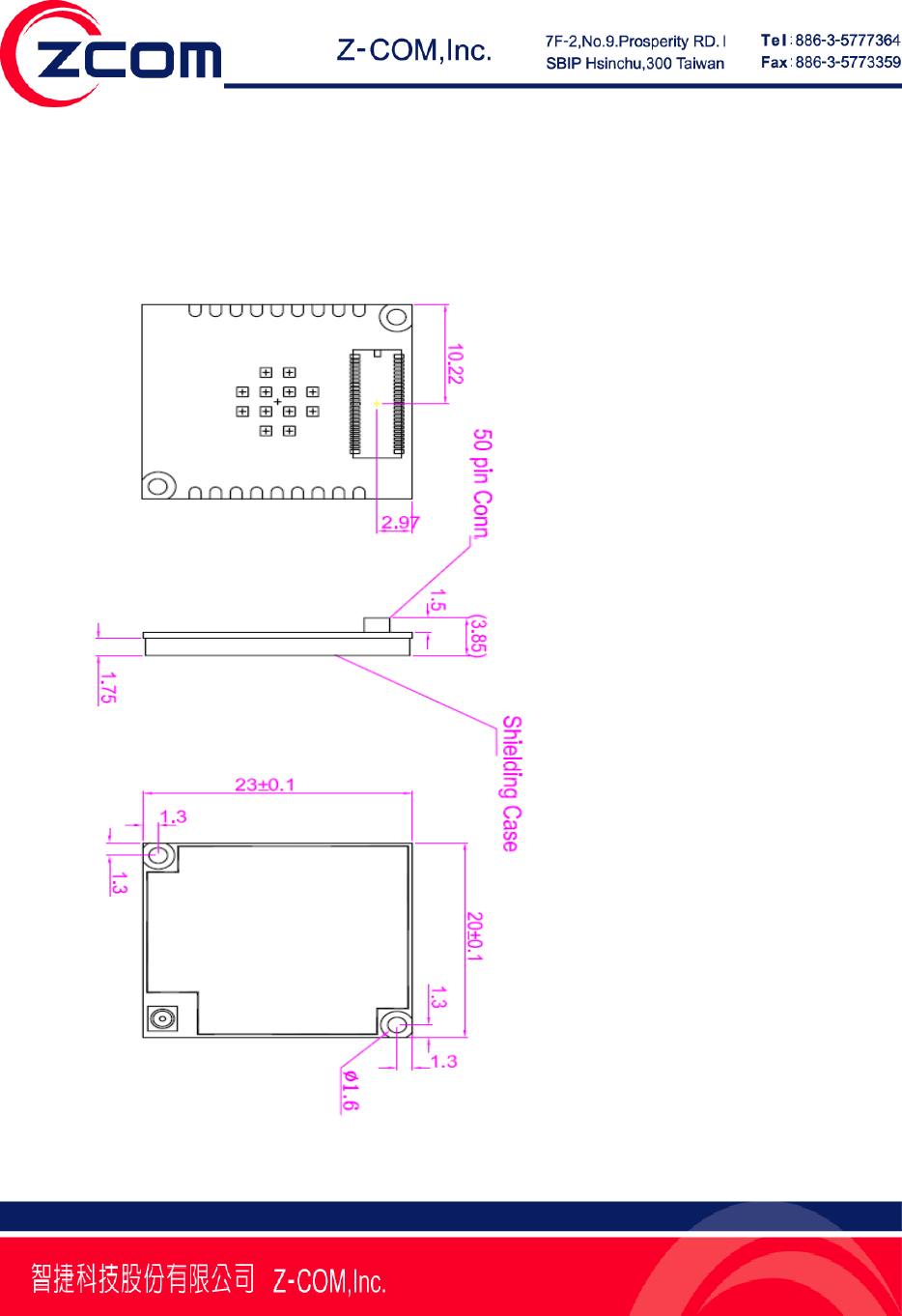
Dimension 20mm(L)*23mm(W)*3.85mm(H)
Weight TBD
2.2 Firmware Specification
Feature Additional Information
Standard - IEEE 802.11i security standard
- IEEE 802.1x security standard
- IEEE 802.11e standard
Operating Mode - Infrastructure mode
- Ad-hoc mode
Power Management - Power save mode
- Deep sleep mode
Security - WPA/WPA2/WPA-PSK/WPA2-PSK
- 40- and 128-bit WEP
- EAP-TLS/EAP-TTLS/EAP-PEAP
Supported OS - WinCE 5.0
- Linux 2.6

Proprietary & Confidential Information
Specifications are subject to change without notice
2.3 Wireless RF Specification
Standard IEEE 802.11g standard
IEEE 802.11b standard
Data Rate 11g: 54M/48M/36M/24M/18M/12M/9/6Mbps
11b: 11Mbps/5.5Mbps/2Mbps/1Mbps
Transmission/Emission Type Direct Sequence Spread Spectrum (DSSS)
Security AES/40- and 128-bit WEP/TKIP
RF Frequency Range USA (FCC): 2.412GHz ~ 2.462GHz (Ch1-11)
Europe (CE): 2.412GHz ~ 2.472GHz (Ch1-13)
Japan (TELEC): 2.412GHz ~ 2.472GHz (Ch1-13)
Data modulation type OFDM/QAM-64/QAM-16/QPSK/BPSK
DSSS/CCK/DQPSK/DBPSK
Output Power +-2dB 11g : 20.09dBm @ 54Mbps
11b : 18.06dBm @ 11/5.5/2/1Mbps
Sensitivity 11g: 54M : -68dBm
11b: 11M : -82dBm
2.4 Pin definition
XG-182M Pin Definition of CON1 (NAIS AXK850145Y) and LGA
CON1
Pin #
LGA
Pin# Pin Name I/O Connection Description
2 17 BT_STATE I 88W8686
Pin.56
Bluetooth State
0 = normal priority, Rx
1 = high priority, Tx
Priority is signaled after BT_PRIORITY has been
asserted. After priority signaling, BT_STATE
indicates the Tx/Rx mode of Bluetooth radio.
3 6 BT_FREQ I 88W8686
Pin.57
4-Wire BCA Mode:
Bluetooth Frequency
Asserted (logic high) when the Bluetooth
transceiver hops into the restricted channels
defined by the coexistence mechanism.
2-Wire, 3-Wire BCA Mode:
Tie to ground (VSS)
4 7 BT_TX_CON O 88W8686 Bluetooth WLAN Active
Proprietary & Confidential Information
Specifications are subject to change without notice
FIRM Pin.58 2-Wire BCA Mode:
When high, WLAN is transmitting or receiving
packets.
3-Wire BCA Mode:
0 = Bluetooth device allowed to transmit
1 = Bluetooth device not allowed to transmit
This pin drives low when PDn is asserted.
In WLAN Sleep mode, all I/O pads are powered
down. This pad must stay at a low state even in
power down mode.
5 8 BT_PRIORIT
Y I 88W8686
Pin.59
Bluetooth Priority
2-Wire BCA Mode:
When high, Bluetooth is transmitting or receiving
high priority packets.
3-Wire BCA Mode:
When high, Bluetooth is transmitting or receiving
packets.
49 9 SDIO_SPI_S
EL O
88W8686
Pin.22 or
Pin.24
High or NC for SDIO, low for SPI interface
9 13 SPI_SDI/SD_
CMD I/O 88W8686
Pin.43
G-SPI Mode: SPI_SDI
G-SPIData Input
SDIO 4-bit Mode: SD_CMD
Command/Response
SDIO 1-bit Mode: SD_CMD
Command Line
SDIO SPI Mode: SD_CMD
Data Input
10 12 SPI_SINTn/
SD_D2 I/O 88W8686
Pin.46
G-SPI Mode: SPI_SINTn
G-SPI Interrupt Output (active low)
SDIO 4-bit Mode: SD_D2
Data Line Bit[2] or Read Wait (optional)
SDIO 1-bit Mode: SD_D2
Read Wait (optional)
SDIO SPI Mode: SD_D2
Reserved
25 11 SPI_SCSn/S
D_D0 I 88W8686
Pin.44
G-SPI Mode: SPI_SCSn
G-SPI Chip Select Input (active low)
SDIO 4-bit Mode: SD_D0
Data Line Bit [0]
SDIO 1-bit Mode: SD_D0
Data Line
SDIO SPI Mode: SD_D0
Data Output

Proprietary & Confidential Information
Specifications are subject to change without notice
32 16 SPI_CLK/SD
_CLK I/O 88W8686
Pin.42
G-SPI Mode: SPI_CLK
G-SPI Clock Input
SDIO 4-bit Mode: SD_CLK
Clock Input
SDIO 1-bit Mode: SD_CLK
Clock Input
SDIO SPI Mode: SD_CLK
Clock Input
34 15 SPI_SDO/SD
_D1 I/O 88W8686
Pin.45
G-SPI Mode: SPI_SDO
G-SPI Data Output
SDIO 4-bit Mode: SD_D1
Data Line Bit [1]
SDIO 1-bit Mode: SD_D1
Interrupt
SDIO SPI Mode: SD_D1
Reserved
35 14 SD_D3 I/O 88W8686
Pin.47
SDIO 4-bit Mode: SD_D3
Data Line Bit [3]
SDIO 1-bit Mode: SD_D3
Reserved
SDIO SPI Mode: SD_D3
Card Select (active low)
39 5 GPIO0 I/O 88W8686
Pin.11
46 4 GPIO1 I/O 88W8686
Pin.40
Internal pull-up
General Purpose Input/Output
These pins are asynchronous to internal clocks.
Several of these pins can be selected to perform
alternate functions such as an LED controller.
When not used, these pins should be left floating.
GPIO1 – LED output (strap pin) (Tx power or Rx
ready LED)
GPIO0 – external oscillator control/SLEEPn;
Wake up control
During power down sleep mode, the external
crystal oscillator is disabled, and, if implemented,
also powered down by GPIO0
13,38 2,3 3.3V
Power ― Power supply from host
1, 50 1,18,1
0 GND Ground ― Ground
6,7,8,1
1,12,1
4,15,1
6,17,1
8,19,2
NC NC NC NC NC
Proprietary & Confidential Information
Specifications are subject to change without notice
0,21,2
2,23,2
4,26,2
7,28,2
9,30,3
1,33,3
6,37,4
0,4142
,43,44,
45,47,
48
Proprietary & Confidential Information
Specifications are subject to change without notice
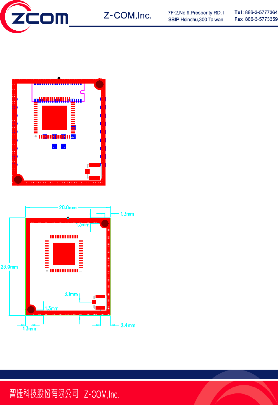
3. Physical Specification
3.1 Mechanical Drawing
Proprietary & Confidential Information
Specifications are subject to change without notice
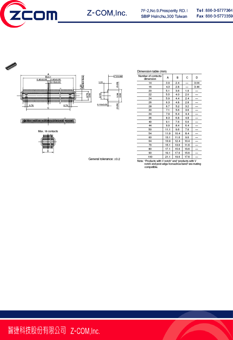
3.2 Connector Drawing
(NAIS AXK850 145Y)
Proprietary & Confidential Information
Specifications are subject to change without notice
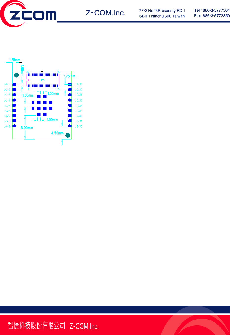
3.3 LGA Drawing
Fig 5.3.1 XG-182M See-Through Drawing
Fig 5.3.2 XG-182M Top View Drawing
Proprietary & Confidential Information
Specifications are subject to change without notice
Fig 5.3.3 XG-182M Bottom View Drawing
Proprietary & Confidential Information
Specifications are subject to change without notice
4. Necessary Approval
(base on customer’s requirement)
4.1 Country Approval
Safety European Union (CE mark) EN60950
EMI North America FCC Part 15 Class B
European Union (CE mark) EN55022 Class B
EN300 328
Telec STD-33
STD-66
VCCI
EMS European Union (CE mark) EN301 489-1
EN301 489-17
Proprietary & Confidential Information
Specifications are subject to change without notice
5. Packaging Specification
The following items will be required for the complete packaging of the Z-Com XG-182M:
Item Comments
EPE Tray z Suitable size and material to protect product
Inner Box z Suitable size and material to protect product
Carton z Suitable size and material to protect product
XG-182M z WLAN module
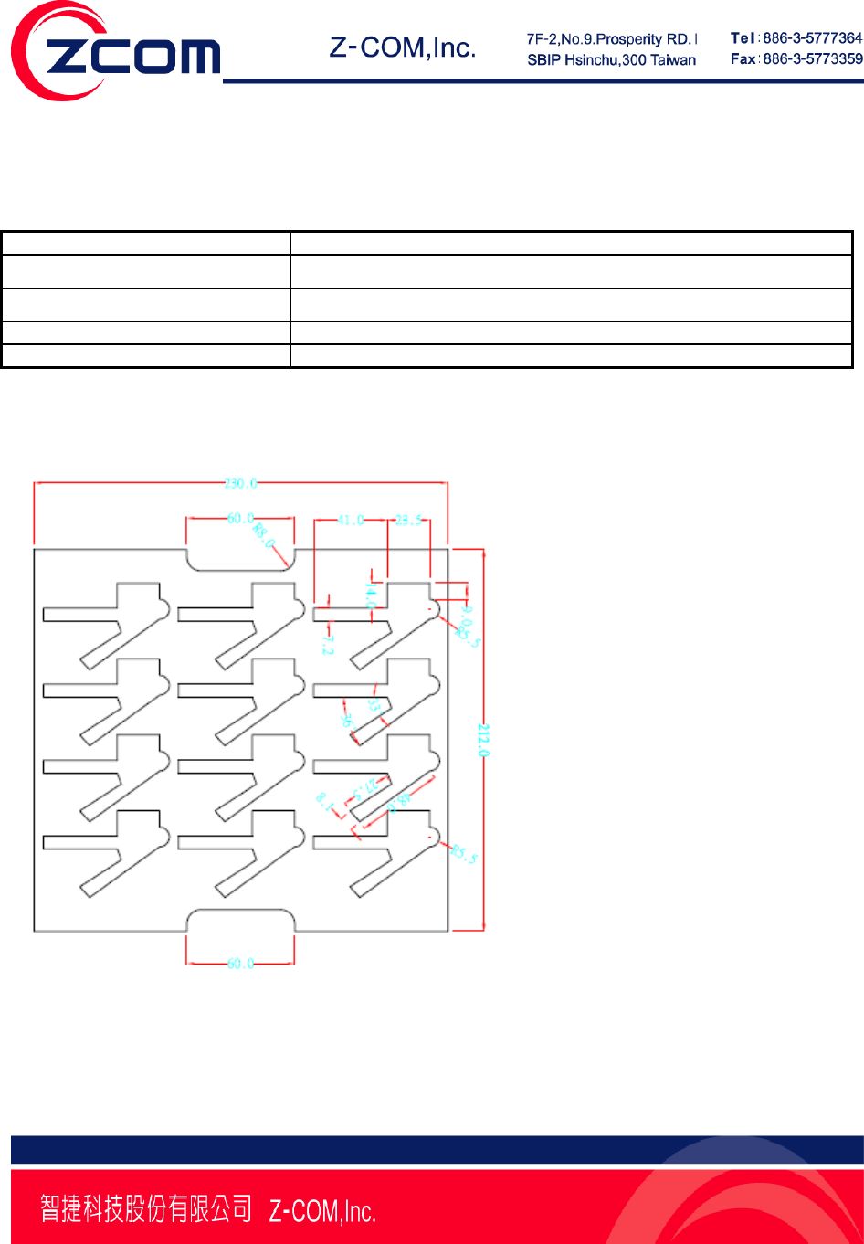
5.1 Package drawing (Reference only)

Proprietary & Confidential Information
Specifications are subject to change without notice
6. Documents:
8.1 Reliability Test Plan: TBD
7. Warranty
One year warranty on the product.
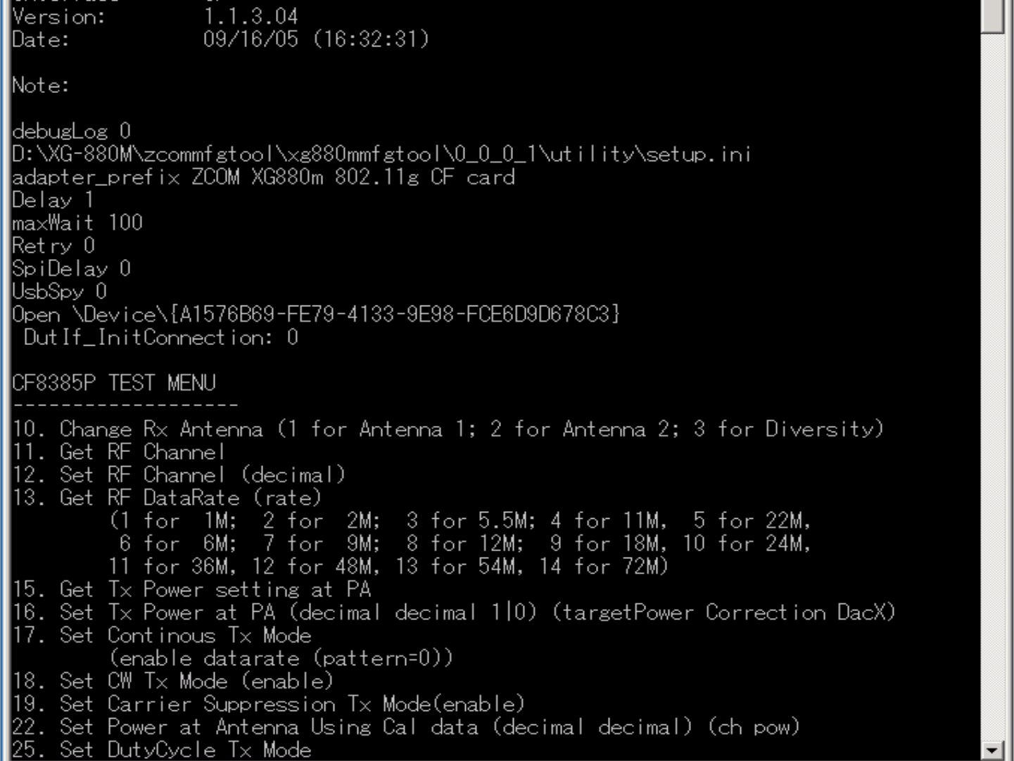
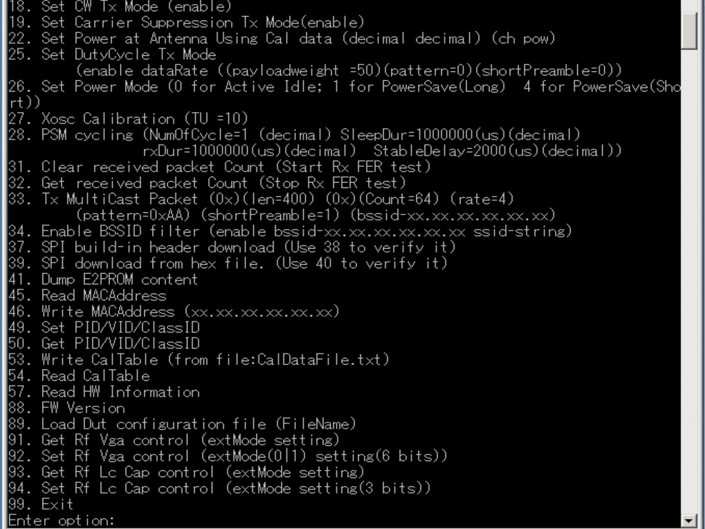
7. Test program

DutApiSD83xxp TX Mode command:
12 1 Chose Antenna
22 1 13 Set target power
25 1 13 Enable Duty Cycle Mode
25 0 Disable
17 1 13 Enable Continuous Mode
17 0 Disable
DutApiSD83xxp Read/Write EEPROM command:
53 Read EEPROM
54 Write EEPROM