ZTE ME3000V2 GSM DUAL BAND GPRS WIRELESS DATA TERMINAL User Manual Q78 ME3000V2
ZTE Corporation GSM DUAL BAND GPRS WIRELESS DATA TERMINAL Q78 ME3000V2
ZTE >
Users Manual

Operation Description
1
ME3000V2 Operation Description
Version:V1.0
ZTE CORPORTION

Operation Description
2
Table of Contents
1 Mechanical Interface ...................................................................................................................... 3
1.1 Physical Features ........................................................................................................................................ 3
1.2 Mechanical size .......................................................................................................................................... 3
2 Electrical Interface ......................................................................................................................... 4
2.1 Pin Assignments ......................................................................................................................................... 4
3 Power Management ....................................................................................................................... 6
3.1 Power and Reset ......................................................................................................................................... 6
3.1.1 Power supply ..................................................................................................................................... 6
3.1.2 Power on ............................................................................................................................................ 6
3.1.3 Power off ........................................................................................................................................... 6
3.1.4 Reset .................................................................................................................................................. 6
4 Antenna Interface ........................................................................................................................... 7
4.1 Antenna Installation ................................................................................................................................... 7
4.2 Antenna Pad ............................................................................................................................................... 7
4.3 Antenna connector ..................................................................................................................................... 7
5 RF Interface ................................................................................................................................... 9
5.1 Overview .................................................................................................................................................... 9
5.2 Antenna Subsystem .................................................................................................................................... 9
5.2.1 Antenna Specifications .................................................................................................................... 10
5.2.2 Cable Loss ....................................................................................................................................... 10
5.2.3 Antenna Gain Minimum Requirements ........................................................................................... 10
5.2.4 Antenna Gain Maximum Requirements .......................................................................................... 10
5.2.5 Antenna Matching ........................................................................................................................... 10
5.2.6 PCB Design Considerations ............................................................................................................. 10
5.2.7 Other Precautions ............................................................................................................................. 10
5.2.8 Grounding .........................................................................................................................................11
6 Test Capabilities ........................................................................................................................... 12
6.1 Test Description ........................................................................................................................................ 12
6.2 GSM Test Equipment and Tools ............................................................................................................... 13
6.2.1 GSM RF Rx Specification ............................................................................................................... 14
6.2.2 GSM RF Tx Specification: .............................................................................................................. 14
6.2.3 High Temperature Operation Test .................................................................................................... 14
6.2.4 Low Temperature Operation Test .................................................................................................... 14
6.2.5 High Temperature Storage Test ....................................................................................................... 14
6.2.6 Low Temperature Storage Test ........................................................................................................ 15
6.2.7 High Temperature High Humidity Operation Test .......................................................................... 15
6.2.8 Temperature Concussion Test ......................................................................................................... 15
6.2.9 ESD Immunity Test ......................................................................................................................... 15
6.2.10 Radiated Emissions Test .................................................................................................................. 15
Operation Description
3
1 Mechanical Interface
1.1 Physical Features
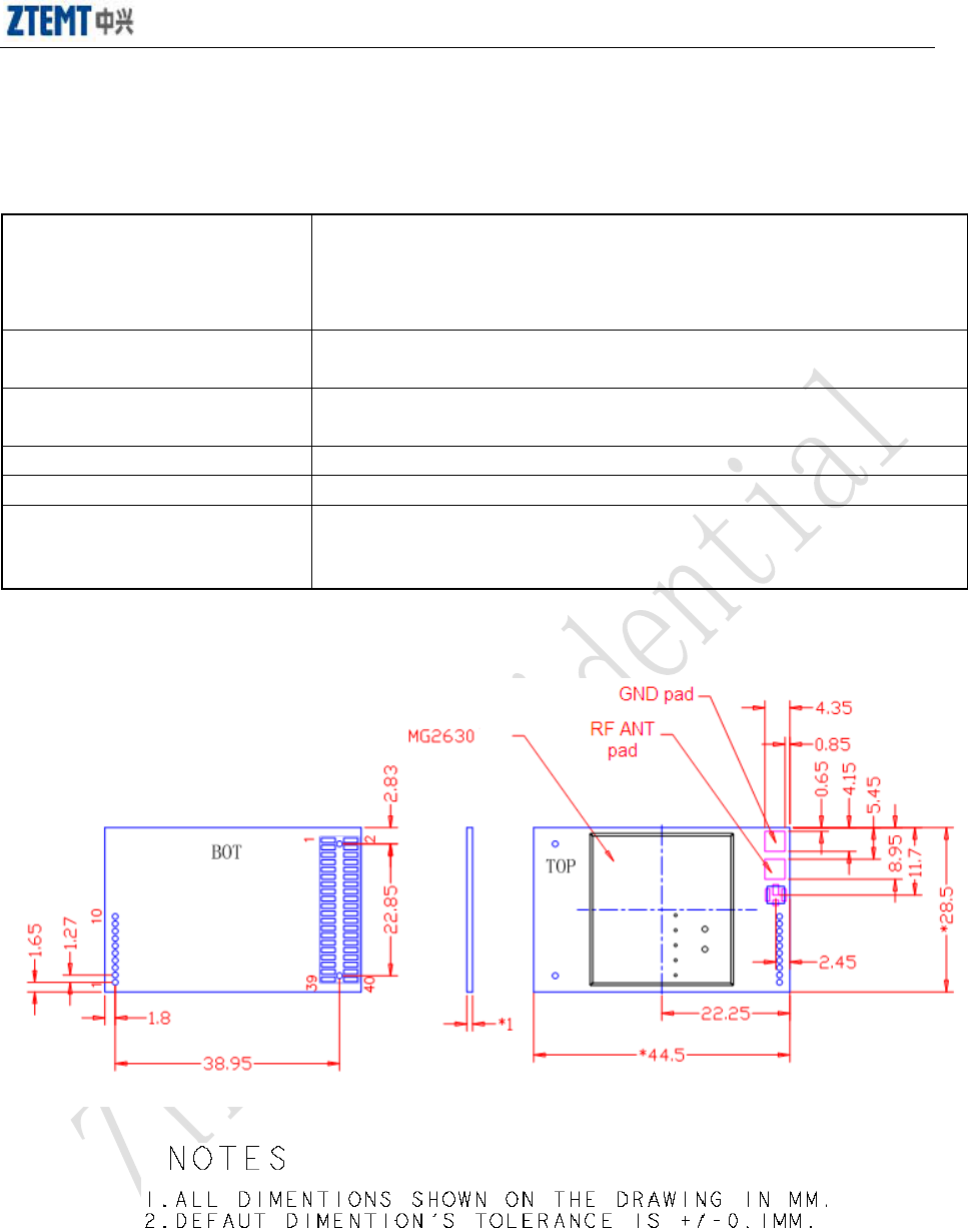
Dimensions & Weight
Length: 44.5 mm
Width: 28.5 mm
Thickness: 8.25 mm
Weight: 8 g
Operational
Temperature Range -20℃ to +65℃
Storage Temperature
Range -40℃ to +80℃
ROHS Yes
Antenna Connectors 50-Ohm ANT connectors for GSM
Power Supply
Two kinds of inputs:
1.external power supply (+4.75V~ +5.25V, typical value +5V)
2. battery power supply (+3.3V~ +4.2V, typical)
1.2 Mechanical size
Figure 1-1: ME3000V2 T-viewgraph
Operation Description
4
2 Electrical Interface
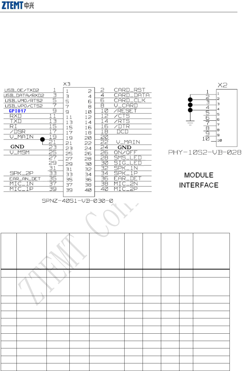
2.1 Pin Assignments
Figure 2-1 ME3000V2 Module interface ME3000V2 map
Table 2-1 ME3000V2 Module 40-pin Electrical Interface
Pin Signeal
Name Signal
Type
Inpu
t/Out
put Function Min Typ Max Uni
t Comments
6 SIM-CLK Digital O SIM clock 2.5 2.8 3.3 V 2.8VLevel
8 SIM-VCC Power O SIM power
supply 2.5 2.8 3.3 V 2.8VLevel
4 SIM-DATA Digital I/O SIM data 2.5 2.8 3.3 V 2.8VLevel
2 SIM-RST Digital O SIM reset 2.5 2.8 3.3 V 2.8VLevel
30 SIG_LED Digital O LED control 2.5 2.8 3.3 V 2.8VLevel
3 RXD2 Digital O COM Port 2.5 2.8 3.3 V 2.8VLevel
11 RXD Digital O COM Port 2.5 2.8 3.3 V 2.8VLevel
1 TXD2 Digital I COM Port 2.5 2.8 3.3 V 2.8VLevel
13 TXD Digital I COM Port 2.5 2.8 3.3 V 2.8VLevel
30 SIG_LED Digital O LED control 2.5 2.8 3.3 V 2.8VLevel
28 SMS_LED Digital O LED control 2.5 2.8 3.3 V 2.8VLevel
22 V_MAIN Power P Main power 3.3 3.7 4.25 V
Operation Description
5
25 V_MSM Power O External
power supply 2.5 2.8 3.3 V
15 RI Digital O 2.5 2.8 3.3 V
LED ON as
the level is
high.
17 /DSR Digital O COM Port 3.3 3.8 4.2 V
14 /RTS Digital I COM Port 3.3 3.8 4.2 V
16 /DTR Digital I COM Port 4.75 5 5.25 V
5 RTS2 Digital I COM Port 3.0 3.8 4.25 V
12 /CTS Digital O COM Port 2.5 2.8 3.3 V
7 CTS2 Digital O COM Port 2.5 2.8 3.3 V
18 DCD Digital O COM Port 2.5 2.8 3.3 V
10 /RESET Digital I System reset 2.5 2.8 3.3 V
26 ON/OFF Digital I Power on/off
key control 2.5 2.8 3.3 V
35 EAR_ANT_D
ET Analog I EARPHONE
MIC KEY
36 EAR_DET Digital I EARPHONE
insert detect
37 MIC_1N Analog AI Mic input-
Headset MIC
39 MIC_1P Analog AI Mic input+
38 MIC_2P Analog AI Mic input+
Earphone
MIC
40 MIC_2N Analog AI Mic input-
32 SPK_1N Analog AO Speaker
output-
Headset
Receiver
34 SPK_1P Analog AO Speaker
output-
33 SPK_2P Analog AO Speaker
output-
Earphone
Receiver
Operation Description
6
3 Power Management
3.1 Power and Reset
3.1.1 Power supply
The module could work under two power modes: 1. Charger; 2 Battery.
When powered by the charger, you could perform constant current charge, constant voltage
charge and trickle current charge. Normally, trickle current charge starts when the voltage is
lower than 3.2V, constant current charge starts as the voltage is between 3.2V and 4.0V; and
constant voltage charge starts when the voltage reaches 4.0V. As the blackout happens, the
battery would be immediately used.
See table 4-1 for the module’s input voltage characteristics. If the input voltage is not in the
range, it must be converted to the voltage below:
Table4-1 Voltage Characteristics
1. External power supply
Status Max. voltage Typical voltage Min. voltage
Power supply +5.25 VDC +5.0VDC +4.75 VDC
2. Battery(currently the software supports Li battery)
Status Max. voltage Typical voltage Min. voltage
Power supply +4.25 VDC +3.8 VDC +3.3 VDC
3.1.2 Power on
The module is under power-off status after it’s normally powered on. To turn on the module,
provide a 1500-2000mS low level pulse to ON/OFF pin when the module is OFF.
3.1.3 Power off
To turn off the module, provide a 1500-2000mS low level pulse to ON/OFF pin when the
module is ON.
3.1.4 Reset
Use the above method to firstly “Power off” and then “Power on”, and by doing so the module
could be reset. ME3000V2 module does not lead the reset pin.

Operation Description
7
4 Antenna Interface
The RF interface of the ME3000V2 Module has an impedance of 50 . The module is capable of sustaining a
total mismatch at the antenna connector or pad without any damage, even when transmitting at maximum RF
power.
The external antenna must be matched properly to achieve best performance regarding radiated power,
DC-power consumption, modulation accuracy and harmonic suppression. Antenna matching networks are not
included on the ME3000V2 Module PCB and should be placed in the host application.
Regarding the return loss, the Module provides the following values in the active band:
Table 4-1 Return Loss in the Active Band
State of Module Return Loss of Module Recommended Return Loss of
Application
Receive ≥ 8dB ≥ 12dB
Transmit not applicable ≥ 12dB
The connection of the antenna or other equipment must be de coupled from DC voltage. This is necessary
because the antenna connector is DC coupled to ground via an inductor for ESD protection.
4.1 Antenna Installation
To suit the physical design of individual applications, the ME3000V2 offers two alternative approached to
connecting the antenna:
■ Recommended approach: MM9329-2700B antenna connector manufactured by MURATA assembled on the
component side of the PCB (top view on Module). See Section 4.3 for details.
■ Antenna pad and grounding plane placed on the bottom side. See Section 4.2 for details.
The MM9329-2700B connector has been chosen as antenna reference point (ARP) for the ZTEMT reference
equipment submitted to type approve the ME3000V2 Module. All RF data specified throughout this manual are
related to the ARP. For compliance with the test results of the ZTEMT type approval you are advised to give
priority to the connector, rather than using the antenna pad.
Note: Both solutions can be applied alternatively. This means,if the antenna is connected to the pad, then the
connector on the Module must be left empty,and when the antenna is connected to the Module connector, the pad
is useless,
4.2 Antenna Pad
The antenna pad of the module is soldered to the board on the customer design to connect with RF line.
For proper grounding connect the RF line to the ground plane on the bottom of the MG2636 Module which
must be connected to the ground plane of the application.
Consider that according to GSM recommendations as 50Ω connector is mandatory for type approval
measurements. It must be ensured that the RF line which is connected to antenna pad should be controlled on
50Ω.
Notes on soldering
■ To prevent damage to the Module and to obtain long-term solder joint properties, you are advised to
maintain the standards of good engineering practice for soldering.
Material Properties
■ME3000V2 Module PCB: FR4
■ Antenna pad: Gold plated pad
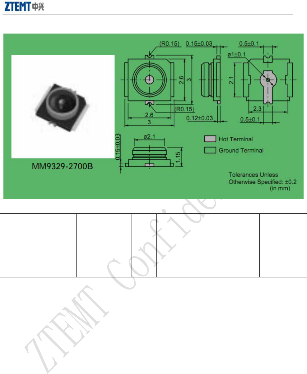
4.3 Antenna connector
The ME3000V2 Module uses a microwave coaxial connector supplied by Murata Ltd. The product name is
MM9329-2700B. The position of the antenna connector on the Module PCB can be seen in Figure 4-1.
Operation Description
8
Figure 4-1 Specification of MM9329-2700B connector
Table 4-2 Product specifications of MM9329-2700B connector
Part
Number
Rated
Voltag
e
(V)
Contact
Resistan
ce
(ohm)
Withstandi
ng
Voltage
(rms)
Insulatio
n
Resistan
ce
(M ohm)
Durabili
ty
(cycles)
Frequen
cy
Rating
(GHz)
Temperatu
re
Range
(degree C)
VSWR Center
Conta
ct
Outer
Conta
ct
Insulator
MM9329
-2700B
250 0.015
max. 300 (AC) 500 min. 100 DC - 6.0 -40~+90 1.2 max.
(DC~3GH
z)
Copper
Alloy
Gold
plated
Copper
Alloy
Silver
plated
Engineeri
ng plastic
Impedance : 50 ohm
Operation Description
9
5 RF Interface
5.1 Overview
A 50 ohm coaxial RF connector is provided for Module testing. However, we advise customers lead from the
antenna pad at the RF line to the antenna.
Figure 5-1 GSM Connector
The module must provide a suitable antenna that works in the desired frequency band of operation. The Antenna
connected to the GSM connector should be a dual band antenna supporting the GSM900 and DCS1800 bands.
Band TX Frequency RX Frequency
GSM 880~915 MHz 925~960 MHz
DCS 1710~1785 MHz 1805~1880 MHz
Note: TX refers to the transmit from the module into the antenna (Reverse Link of the GSM
system), and RX refers to the receive from the antenna into the module (Forward Link of the
GSM system).
5.2 Antenna Subsystem
The antenna sub-system and its design is a major part of the final product integration. Special attention and care
should be taken in adhering to the following guidelines.

Operation Description
10
5.2.1 Antenna Specifications
Choice of the antenna cable (type, length, performance, RF loss, etc) and antenna connector (type + losses) can
have a major impact on the success of the design.
5.2.2 Cable Loss
All cables have RF losses. Minimizing the length of the cable between the antenna and the RF connectors on the
module will help obtain superior performance. High Quality/Low loss co-axial cables should be used to connect
the antenna to the RF connectors. Contact the antenna vendor for the specific type of cable that interfaces with
their antenna and ask them to detail the RF losses of the cables supplied along with the antenna. Typically, the
cable length should be such that they have no more than 1-2dB of loss. Though the system will work with longer
(loss) cables, this will degrade GSM system performance. Care should also be taken to ensure that the cable end
connectors/terminations are well assembled to minimize losses and to offer a reliable, sturdy connection to the
Module sub-system. This is particularly important for applications where the module is mounted on a mobile or
portable environment where it is subject to shock and vibration.
5.2.3 Antenna Gain Minimum Requirements
It is recommended that the antenna chosen have at least 2 dBi gain in the GSM900 band and 4 dBi in the PCS
band. The Antenna subsystem shall also have at least 8 dB of return loss at the input with respect to a 50-ohm
system.
5.2.4 Antenna Gain Maximum Requirements
Our FCC Grant imposes a maximum gain for the antenna subsystem: 7 dBi for the GSM900 band and 13dBi for
the DCS band.
Warning: Excessive gain could damage sensitive RF circuits and void the warranty.
5.2.5 Antenna Matching
The module’s RF connectors are designed to work with a 50-ohm subsystem. It is assumed that the antenna
chosen has matching internal to it to match between the 50-ohm RF connectors and the antenna impedance.
5.2.6 PCB Design Considerations
• The antenna subsystem should be treated like any other RF system or component. It should be isolated as much
as possible from any noise generating circuitry including the interface signals via filtering and shielding.
• As a general recommendation all components or chips operating at high frequencies such as
micro controllers, memory, DC/DC converts and other RF components should not be placed too close to the
module. When such cases exist, correct supply and ground de-coupling areas should be designed and validated.
• Avoid placing the components around the RF connection and close to the RF line between the RF antenna and
the module.
• RF lines and cables should be as short as possible.
• If using coaxial cable it should not be placed close to devices operating at low frequencies. Signals like charger
circuits may require some EMI/RFI decoupling such as filter capacitors or ferrite beads.
• Adding external impedance matching to improve the match to your cable and antenna assemblies is optional.
Please contact the antenna vendor for matching requirements.
• For better ESD protection one can implement a shock coil to ground and place it close to the RF connector.
5.2.7 Other Precautions
It is essential to keep the voltage ripple to a minimum at this connection in order to avoid phase error. Insufficient
power supply voltage can dramatically affect some RF performance such as TX power, modulation spectrum
EMC performance, and spurious emissions and frequency error.
The RF connections are 50-ohm impedance systems and are a DC short to ground. Best effort should be made to
provide low insertion loss and shielding between the external antenna and RF connections over the frequency
band of interest.

Operation Description
11
5.2.8 Grounding
On terminals including the antenna, poor shielding can dramatically affect the sensitivity of the terminal.Moreover
the power emitted through the antenna can affect the application.
Operation Description
12
6 Test Capabilities
6.1 Test Description
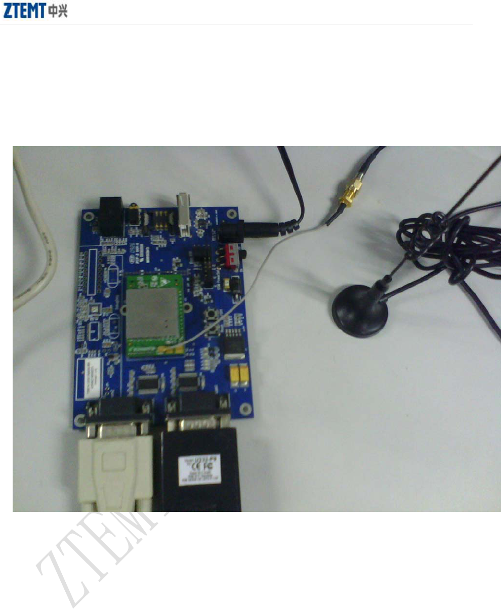
1) ME3000V2 RF Connectors:
2) Operating instructions
Operation Description
13
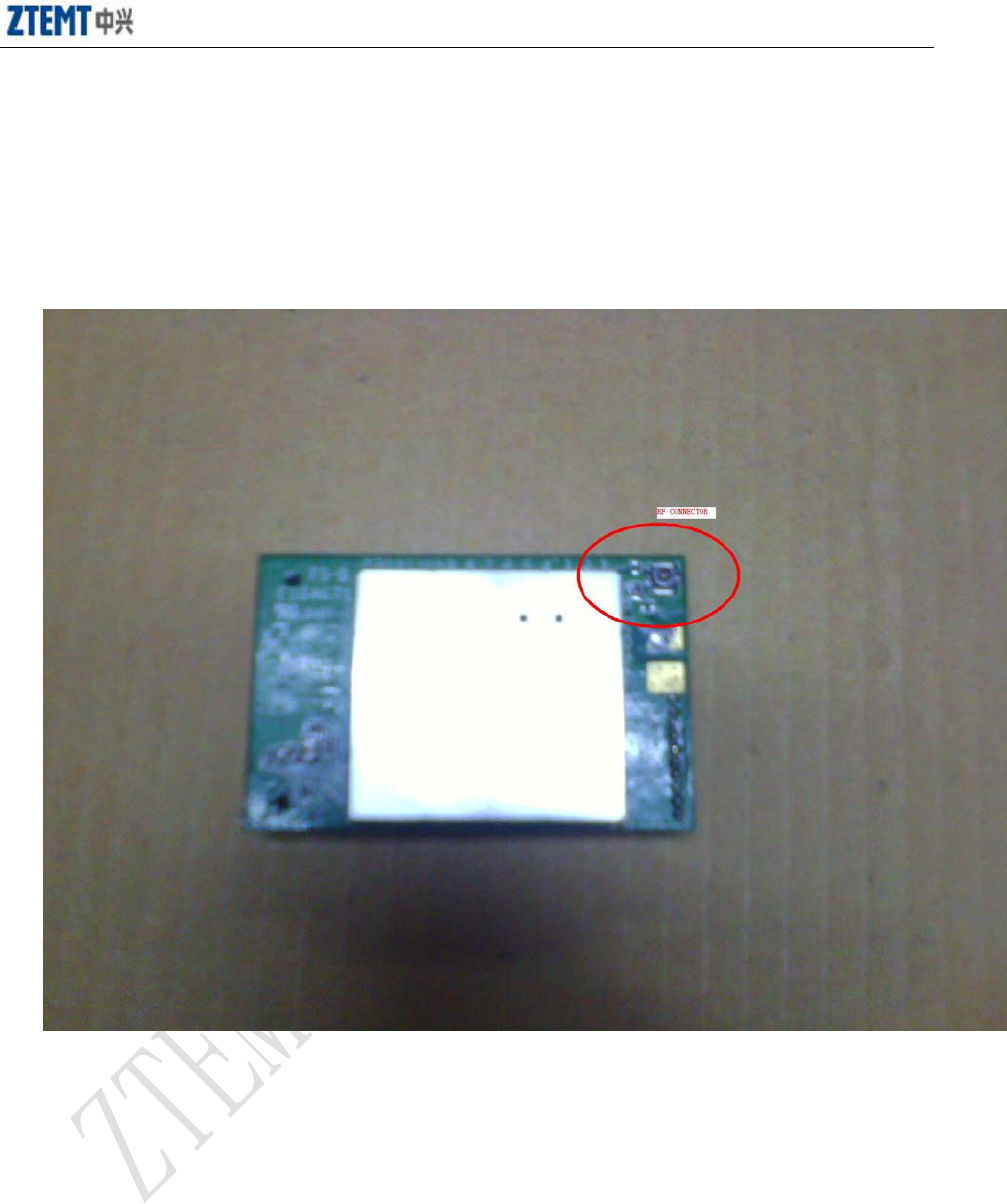
Connect the sector to access terminal antenna connectors as shown in the following figure 6-1
figure 6-1
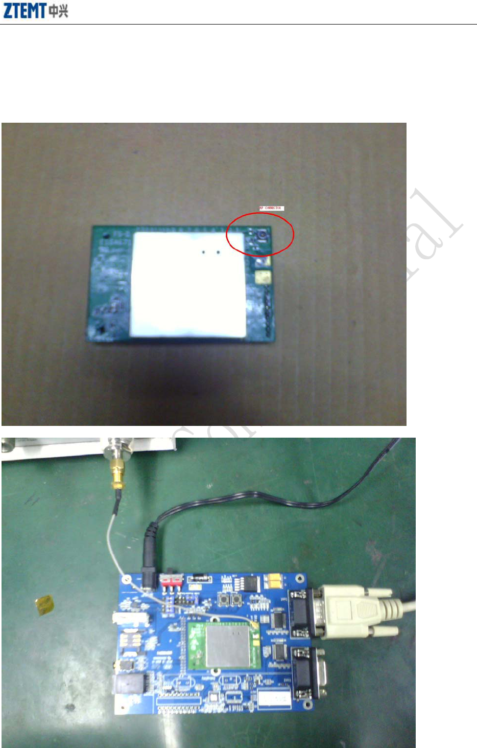
Connect the sector to access terminal antenna connectors as shown in the following figure 6-2:
figure 6-2
6.2 GSM Test Equipment and Tools
Lease or purchase of test equipment is available from vendors who provide this equipment for GSM over the-air
simulation. Some suggested products include:
• Agilent 8960 Series 10 E5515C CDMA Mobile Station Tester
• Agilent E4440A Spectrum analyzer
• Agilent E4438C Signal Generator
• Agilent E4438C Signal Generator
• Programmable Temperature-Humidity Testor
• Programmable Temperature Concussion Testor
RF Performance Requirements
Operation Description
14
6.2.1 GSM RF Rx Specification
Frequency range 925~960 MHz/1805~1880 MHz
Rx. Sensitivity -109 dBm for GSM, -108dBm for DCS (BER≤2.4%)
Rx. Signal Range -25 dBm~ -109dBm(BER≤2.4%)
6.2.2 GSM RF Tx Specification:
Max. frequency tolerance 880~915 MHz/1710~1785 MHz
Max. Tx. Power GSM900: 32.2±1 dBm
DCS1800:29.2±1 dBm
Peak Phase Error -20°< PPE < 20°
RMS Phase Error -5°< RMS < 5°
Frequency Error GSM900: -90Hz< FE <90 Hz
DCS1800: -180Hz< FE <180 Hz
Modulation Spectrum Mod +400kHz: <-60dBm
Mod -400kHz: <-60dBm
Mod+1800kHz:<-63dBm
Mod-1800kHz:<-63dBm
Switching Spectrum Switching +400kHz:<-22dBm
Switching -400kHz:<-22dBm
Switching +1800kHz:<-27dBm
Switching -1800kHz:<-27dBm
Remarks:
RF technical specification conforms to the following standards:
3GPP2 Recommended Minimum Performance Standards for GSM Spread Spectrum Mobile Stations
3GPP2 Recommended Minimum Performance Standards for GSM High Rate Packet Data Access Terminal
Environmental Reliability Requirement
6.2.3 High Temperature Operation Test
EUT Status Power-on
Temperature 70℃
Duration 24h
6.2.4 Low Temperature Operation Test
EUT Status Power-on
Temperature -30℃
Duration 24h
6.2.5 High Temperature Storage Test
EUT Status Power-off
Temperature 85℃

Operation Description
15
Duration 24h
6.2.6 Low Temperature Storage Test
EUT Status Power-off
Temperature -40℃
Duration 24h
6.2.7 High Temperature High Humidity Operation Test
EUT Status Power-on
Temperature 55℃
Humidity 93%
Duration 48h
6.2.8 Temperature Concussion Test
EUT Status Power-off
High Temperature 85℃
High Temperature Duration 1h
Low Temperature -45℃
Low Temperature Duration 1h
Cycle Times 10
ElectroMagnetic Compatibility
6.2.9 ESD Immunity Test
EUT Status Idle mode and traffic mode
Test Voltage Air ±8KV; Contact ±6KV
Reference Standard IEC 61000-4-2 : 2001
6.2.10 Radiated Emissions Test
EUT Status Idle mode and traffic mode
Limits for radiated disturbance Class B ITE
Reference Standard FCC Part 22H&24E