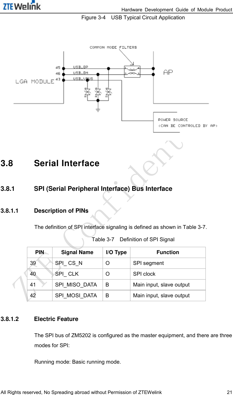
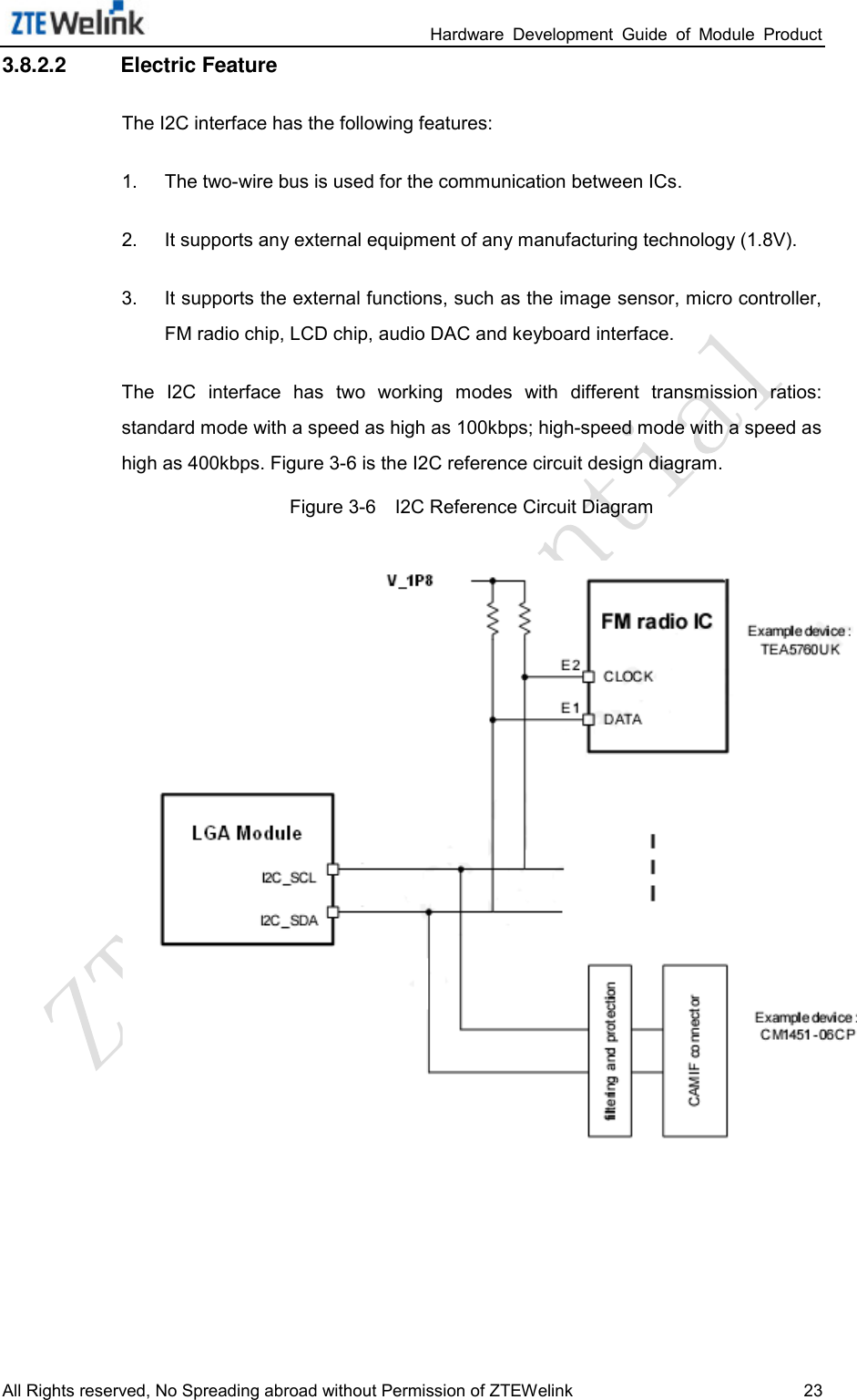
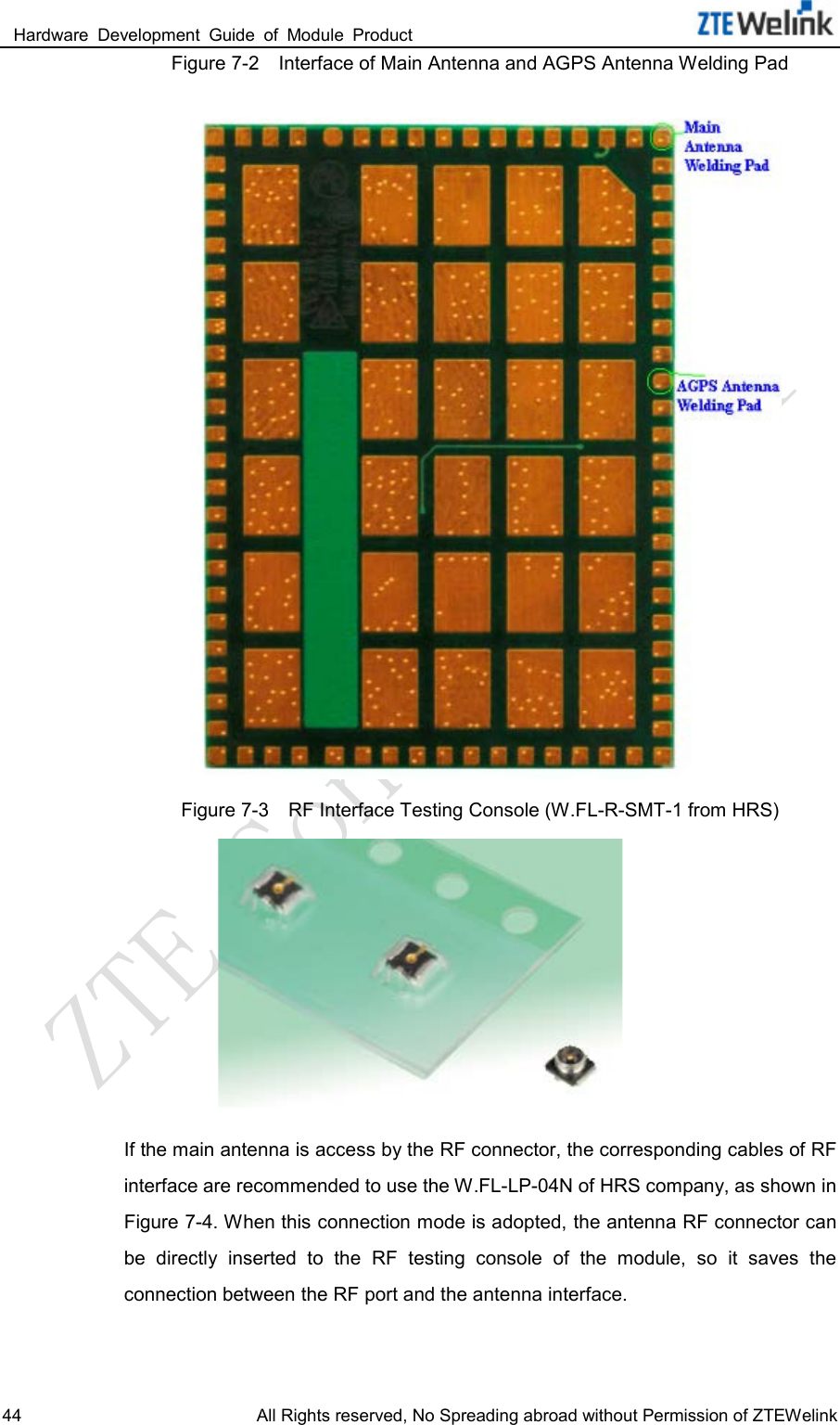
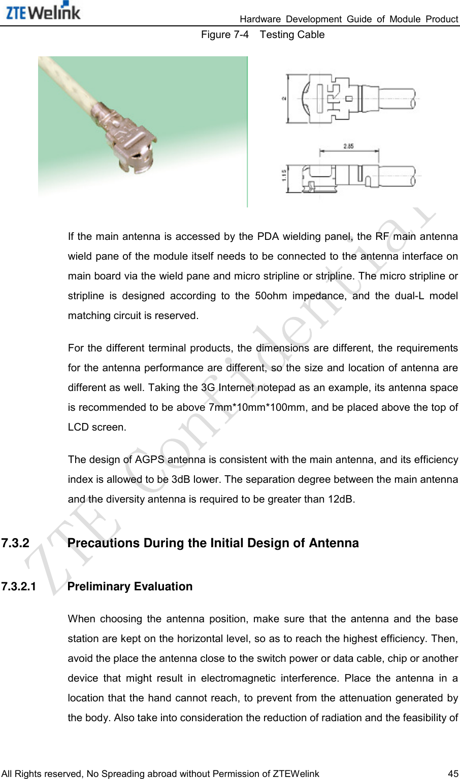
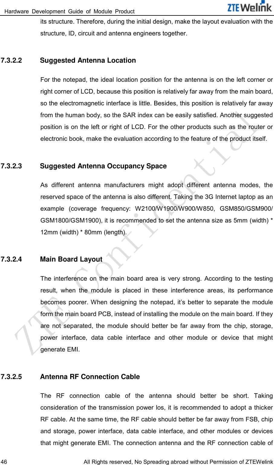
ZTE ZM5202 WCDMA Wireless Data Terminal User Manual
ZTE Corporation WCDMA Wireless Data Terminal Users Manual
UserManual.wiki
>
ZTE
>
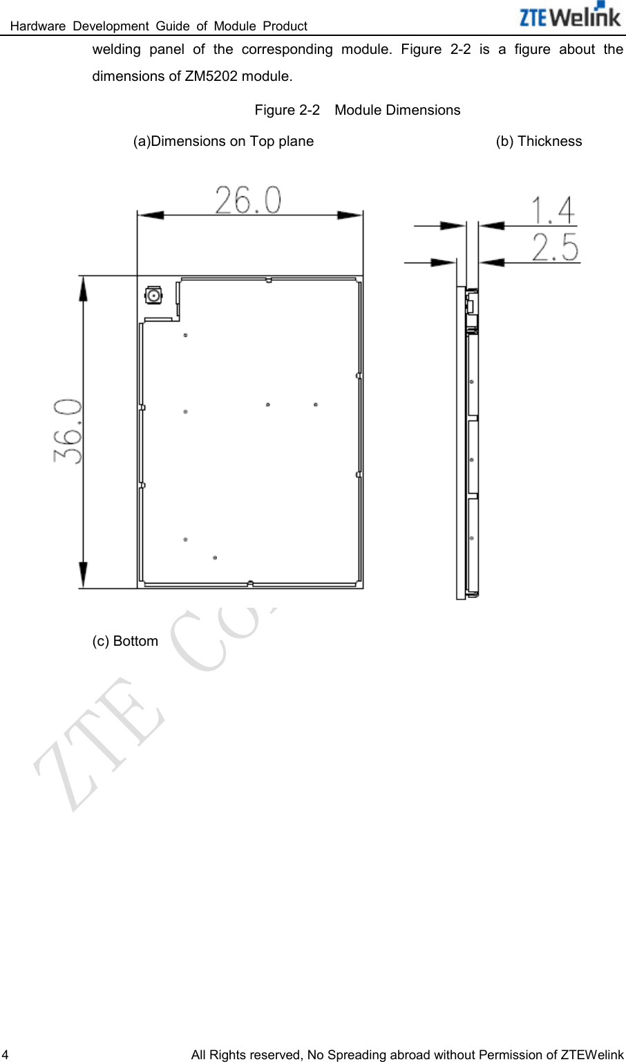
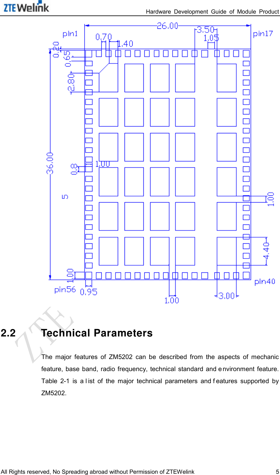
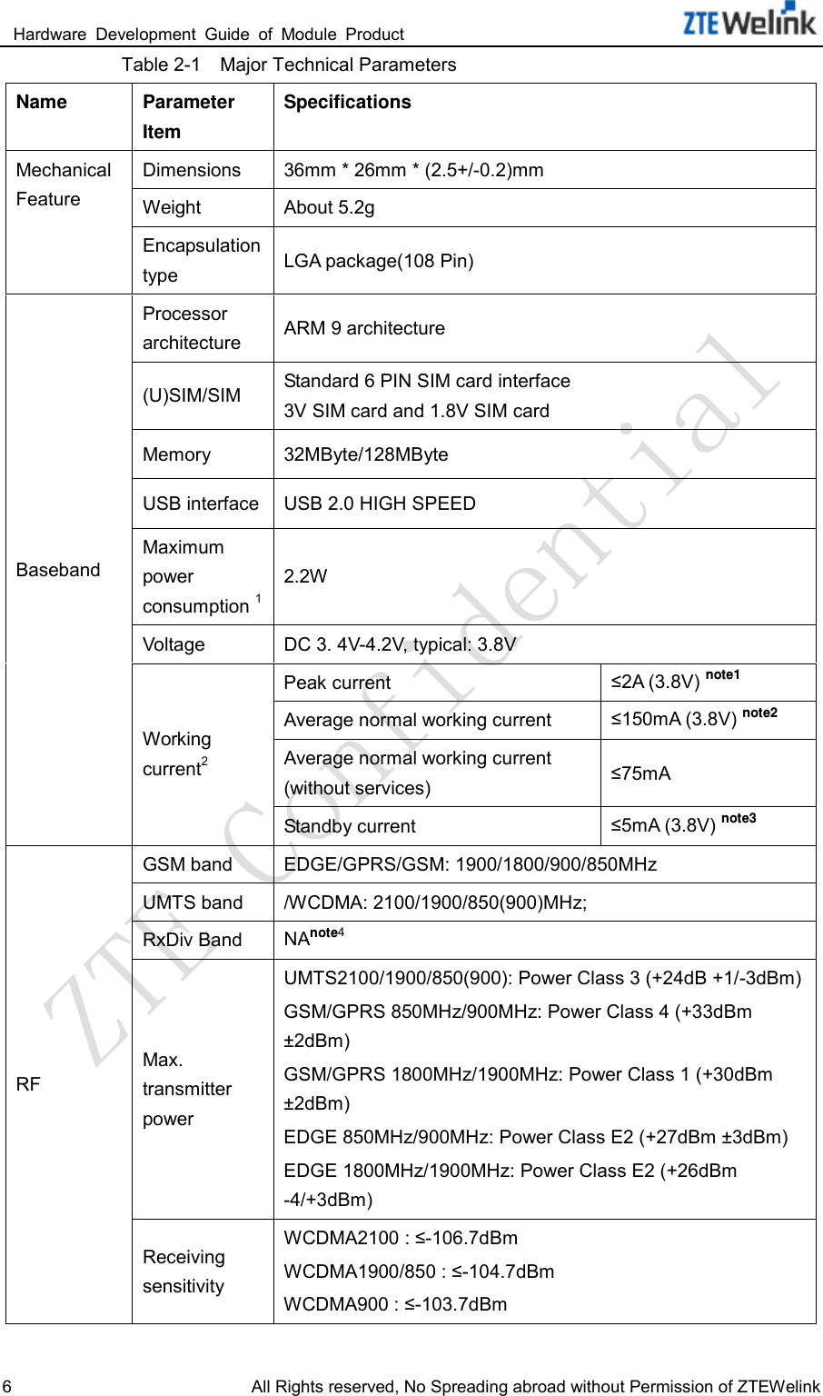
ZM5202 User Manual
User manual
Navigation menu
Upload a User Manual
Namespaces
Wiki Guide
HTML
PDF
Info
Views
User Manual
Discussion / Help
Navigation
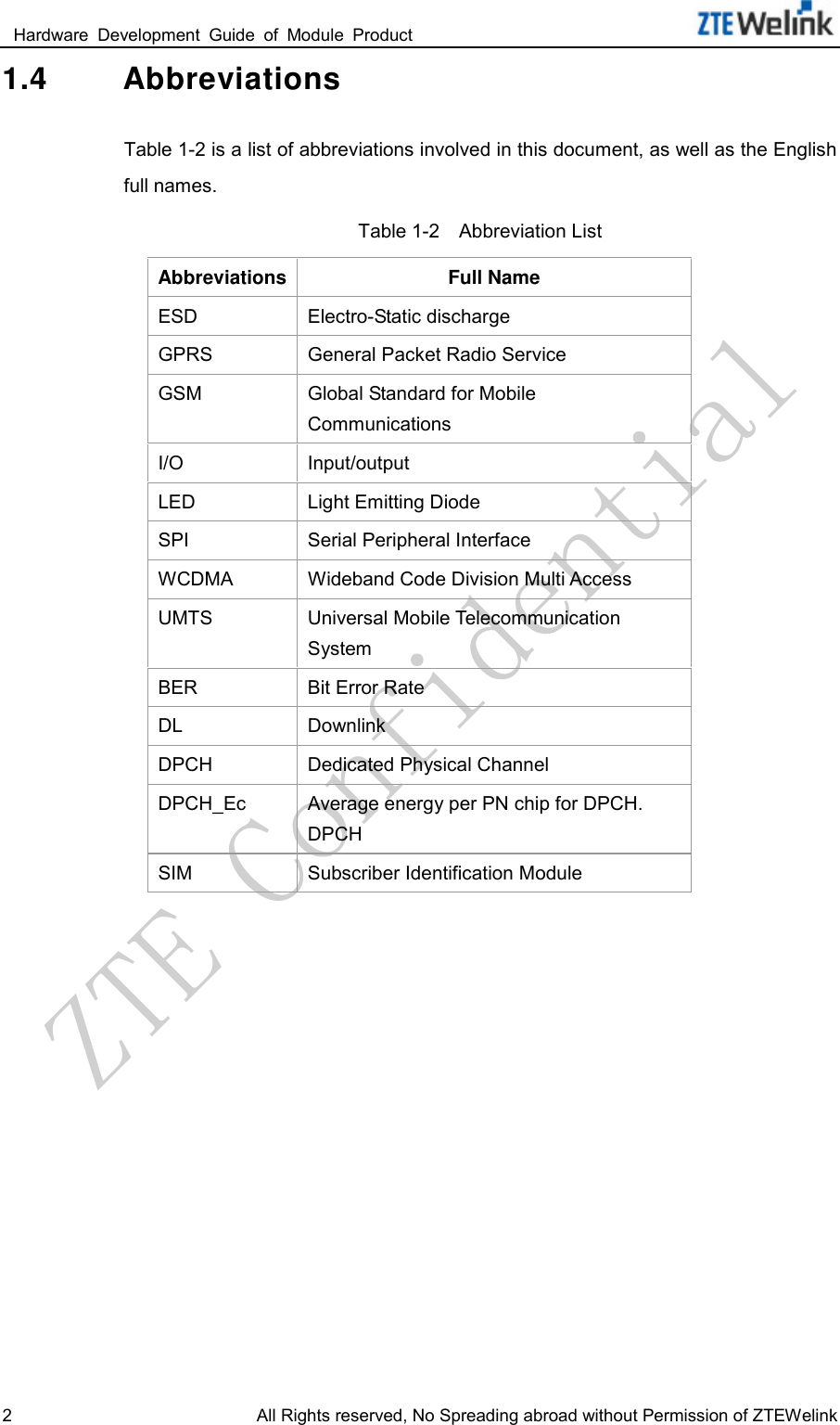
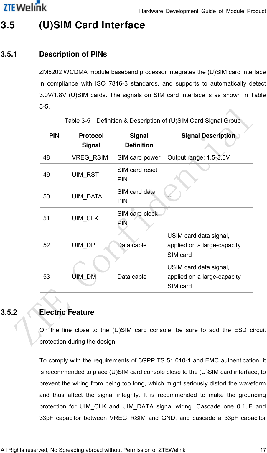
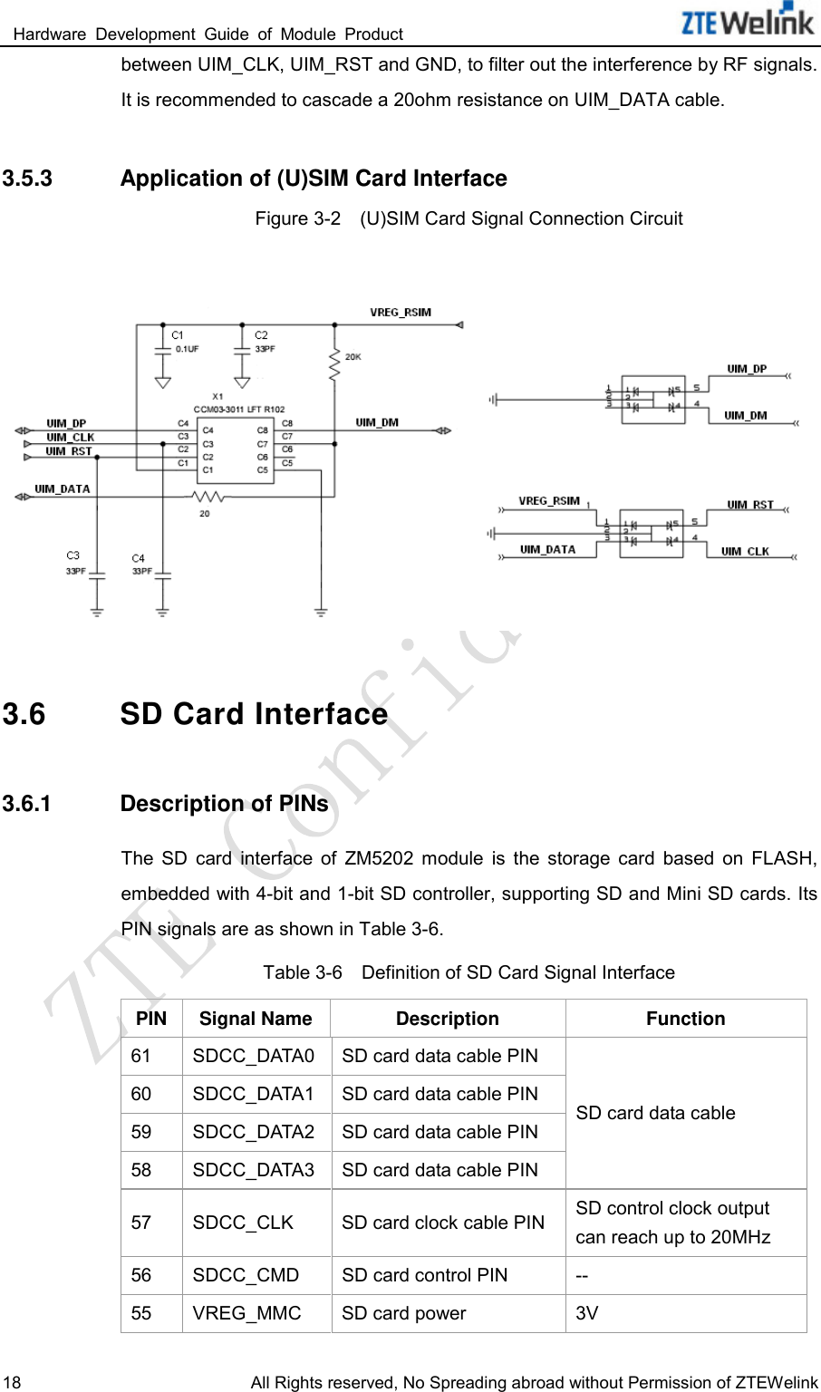
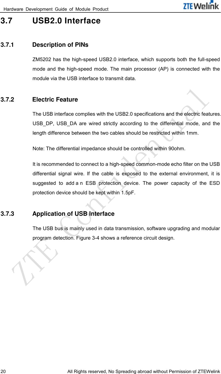
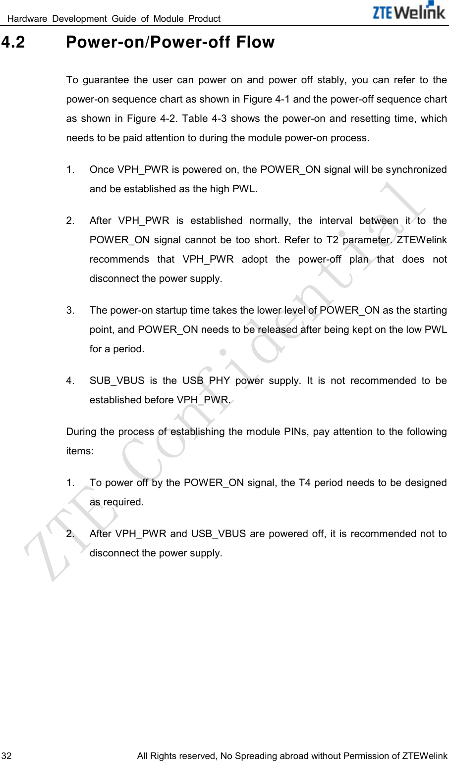
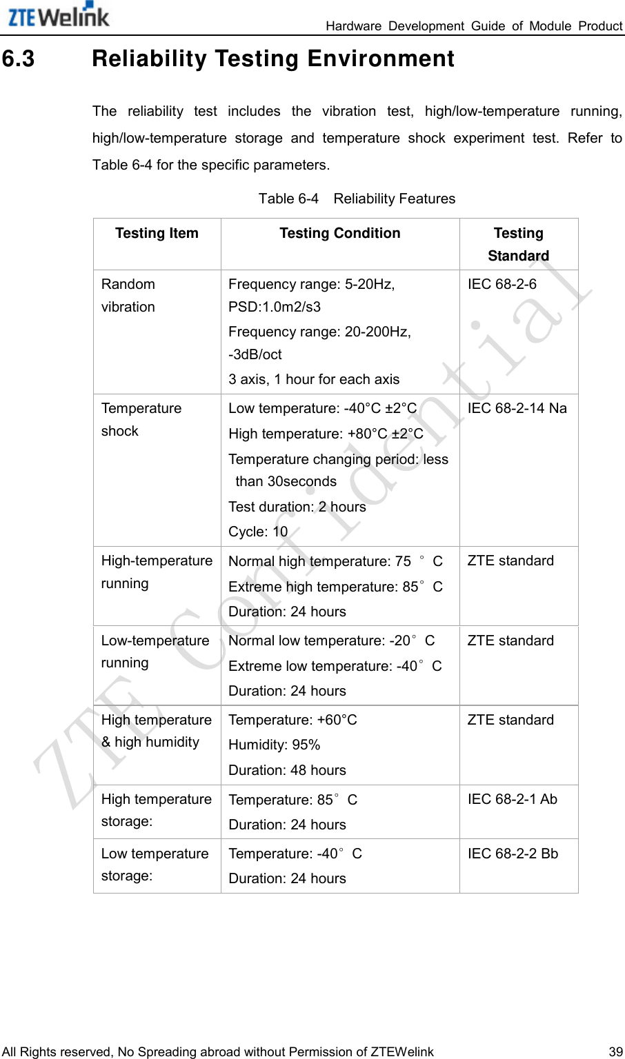
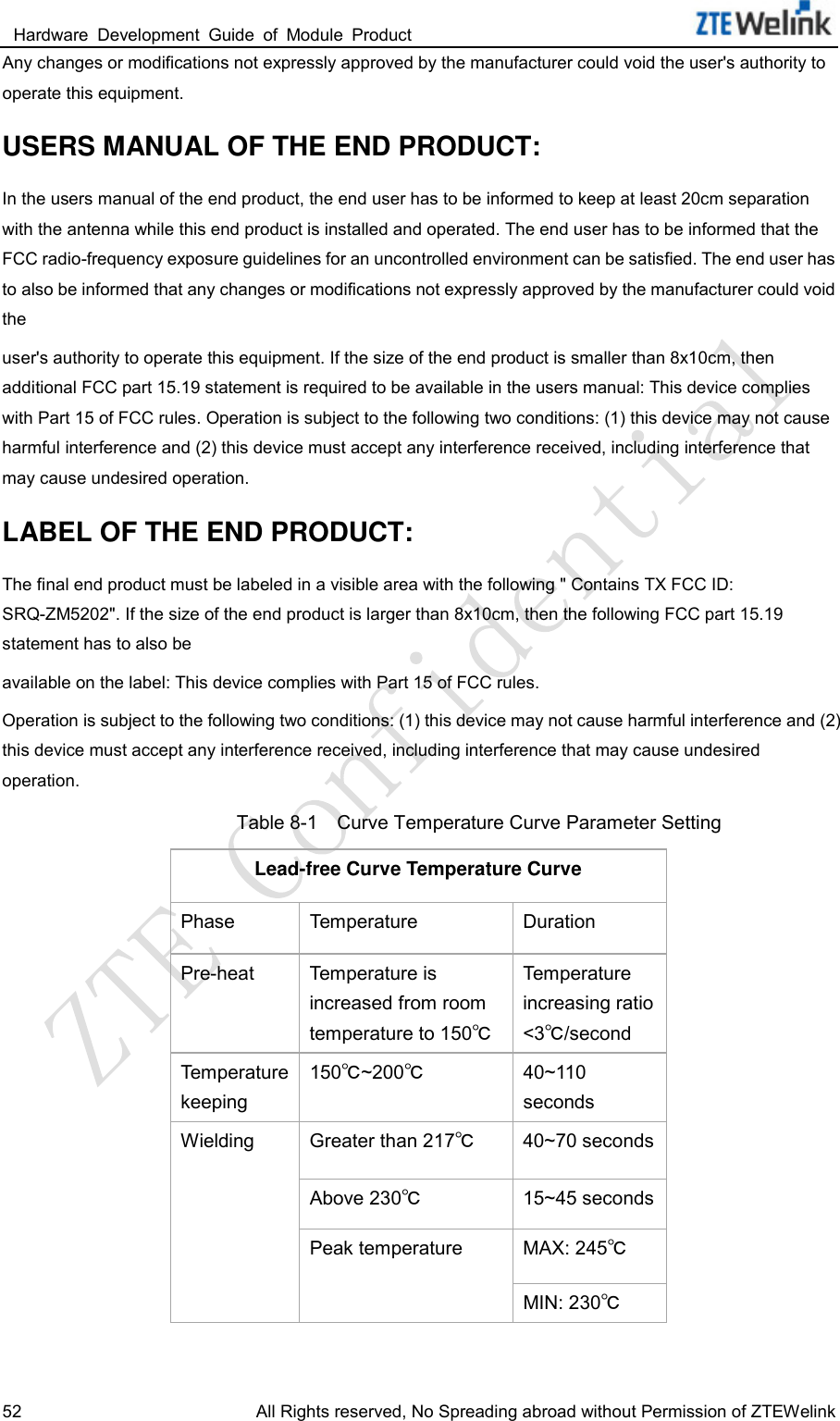
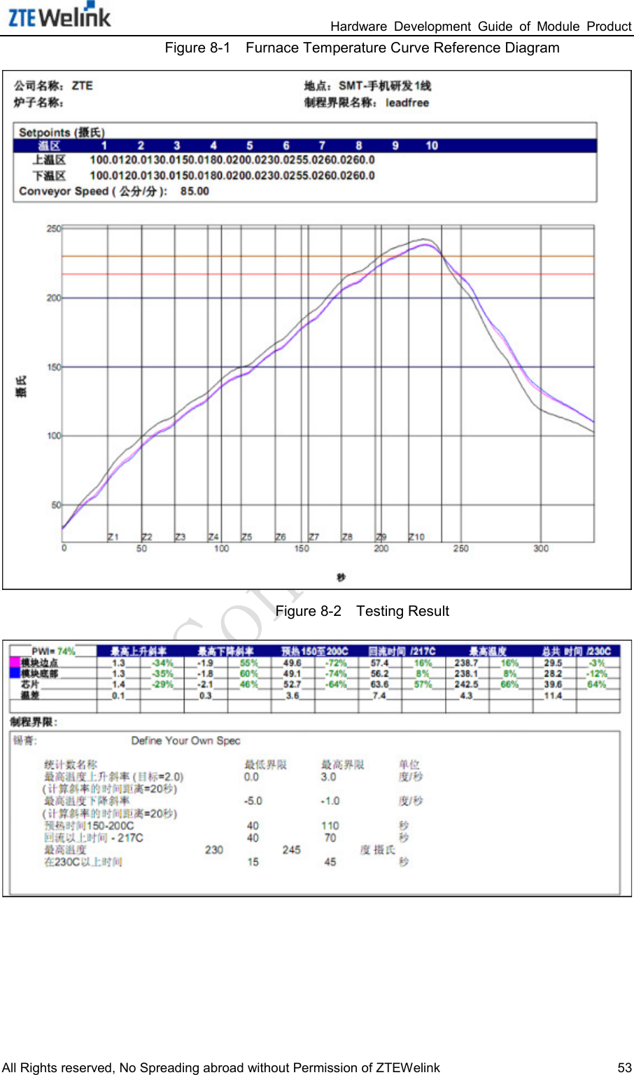
![Hardware Development Guide of Module Product All Rights reserved, No Spreading abroad without Permission of ZTEWelink 19 3.6.2 Electric Feature SDCC_CLK: Clock signal, host2device, default is 0~25MHz. SDCC_CMD: Command/response, two-way: the command can sent from the host to a single card/all cards, the response is sent from a single card/all cards to the host. SDCC_DATA[3..0]: Data cable, two-way, default is 0~12.5MB/sec. 3.6.3 Application of SD Card Interface Figure 3-3 is the reference design diagram for the SD interface. The detection of SD card adopts the polling mode of DATA3 signal cable to judge whether T card is inserted or not. Figure 3-3 SD Typical Application Circuit](https://usermanual.wiki/ZTE/ZM5202/User-Guide-2034889-Page-27.png)