ZTE ZM5202 WCDMA Wireless Data Terminal User Manual
ZTE Corporation WCDMA Wireless Data Terminal Users Manual
ZTE >
User manual
Hardware Development Guide of Module Product
All Rights reserved, No Spreading abroad without Permission of ZTEWelink I
Hardware Development Guide of
Module Product
Product Model No:ZM5202
Document Version: 2.0
Release Date: 2013-05-31
Hardware Development Guide of Module Product
II All Rights reserved, No Spreading abroad without Permission of ZTEWelink
Legal Information
By accepting this certain document of Shenzhen ZTEWelink Technology CO., LTD. (hereinafter
referred to as “ZTEWelink”) you agree to the following terms. If you do not agree to the following
terms, please notice that you are not allowed to use this document.
The copyright of this document belongs to Shenzhen ZTEWelink Technology CO., LTD. Any rights
not expressly granted herein are reserved. This document contains the proprietary information of
ZTEWelink. Any reproduction, transfer, distribution, use, or disclosure of this document or any
picture, form, data or other information contained in this document, in any form by any means,
without the prior written consent of ZTEWelink is prohibited.
And are the registered trademarks of ZTE. is the registered
trademark of ZTEWelink. ZTEWelink is the wholly owned subsidiary of ZTE and is authorized by
the use of the registered trademark of ZTE. ZTE’s company product name, logo, and product
names referenced herein are either trademarks or registered trademarks of ZTE. Other product
and company names mentioned herein may the trademarks or registered trade names of their
respective owners. Without the prior written consent of ZTEWelink or the third party owner thereof,
anyone’s access to this document should not be construed as granting, by implication, estopped
or otherwise, any license or right to use any marks appearing in this document.
The design of this product complies with the requirements of environmental protection and
personal security. This product shall be s tored, used or discarded in accordance with product
manual, relevant contract or laws and regulations in the relevant country (countries).
Information contained in this document is subject to continuous update and modify without further
notice due to improvement and update of ZTEWelink’s products and technologies. At the same
time, ZTEWelink reserves the right to revise and recover this manual at any time.
If there are any unknown words in the user manual, please consult the company or agents,
distributor in a timely manner.
Hardware Development Guide of Module Product
All Rights reserved, No Spreading abroad without Permission of ZTEWelink III
Revision History
Version Date Description
1.0 2010-04-15 1st version
2.0
2013-03-20
1. Delete the part of 3.13 and 3.14 in former version
2. Change Logo of the header, footer and front cover
3. Modify the legal information
2013-05-13
4. Modify the Reference document list in chapter 1.3
5. Add the module dimensions of top plane and thickness
6. Modify the chapter 7.7 of Recommended Product
Upgrading Plan
7. Modify the Standby current from 3.5mA to 5mA in Table
2-1
8. Modify the peak current from ≤470mA to ≤2A and
modify the Working temperature from 70 to 75°C in
Table 2-1
9. Modify the Pin 32-35,64,65,67,68 and description in
chapter 3.1.3
10. Modify chapter 3.8.3 to support of 8 wire UART
11. Modify the MODULE_WAKEUP_AP interface
application
12. Modify the product test environment in Table 6-2 and
6-4
13. Modify the product test result in Table 6-6
14. Update the Figure 3-1 of PIN Configuration Diagram
Modify the Figure 7-2 of Main and AGPS Antenna
Welding Pad Interface
15. Modify the Figure 7-1 of Main Antenna RF Connector
Interface
16. Modify Figure 2-1 of Product Illustration
2013-05-31 17. Release as Version 2.0

Hardware Development Guide of Module Product
IV All Rights reserved, No Spreading abroad without Permission of ZTEWelink
TABLE OF CONTENTS
1 About This Document ..................................................................................... 1
1.1 Application Range ............................................................................................................ 1
1.2 Purpose ............................................................................................................................ 1
1.3 Supported & Reference Document List ........................................................................... 1
1.4 Abbreviations ................................................................................................................... 2
2 Product Overview ............................................................................................ 3
2.1 Mechanic Features .......................................................................................................... 3
2.2 Technical Parameters ...................................................................................................... 5
2.3 Function Overview ........................................................................................................... 8
2.3.1 Baseband Function .......................................................................................................... 8
2.3.2 Radio Frequency Function ............................................................................................... 8
3 Interfaces ....................................................................................................... 10
3.1 Definition of PINs ........................................................................................................... 10
3.1.1 Definition of PIN I/O Parameters .................................................................................... 10
3.1.2 PIN Configuration Diagram ............................................................................................ 10
3.1.3 PIN Description .............................................................................................................. 11
3.2 Working Condition .......................................................................................................... 15
3.3 Feature of Interface Power Level ................................................................................... 16
3.3.1 Feature of Digital Power Level Signal ............................................................................ 16
3.4 Power Interface .............................................................................................................. 16
3.4.1 Description of Power PINs ............................................................................................. 16
3.4.2 Requirement of Power Supply ....................................................................................... 16
3.5 (U)SIM Card Interface .................................................................................................... 17
3.5.1 Description of PINs ........................................................................................................ 17
3.5.2 Electric Feature .............................................................................................................. 17
3.5.3 Application of (U)SIM Card Interface ............................................................................. 18

Hardware Development Guide of Module Product
All Rights reserved, No Spreading abroad without Permission of ZTEWelink V
3.6 SD Card Interface .......................................................................................................... 18
3.6.1 Description of PINs ........................................................................................................ 18
3.6.2 Electric Feature .............................................................................................................. 19
3.6.3 Application of SD Card Interface .................................................................................... 19
3.7 USB2.0 Interface ............................................................................................................ 20
3.7.1 Description of PINs ........................................................................................................ 20
3.7.2 Electric Feature .............................................................................................................. 20
3.7.3 Application of USB Interface .......................................................................................... 20
3.8 Serial Interface ............................................................................................................... 21
3.8.1 SPI (Serial Peripheral Interface) Bus Interface .............................................................. 21
3.8.2 I2C Bus .......................................................................................................................... 22
3.8.3 UART Interface .............................................................................................................. 24
3.9 JTAG (Joint Test Action Group) Interface ...................................................................... 26
3.9.1 Description of PINs ........................................................................................................ 26
3.9.2 Application of JTAG Interface ........................................................................................ 26
3.10 Power-on/Power-off & Reset Signal .............................................................................. 26
3.10.1 Description of PINs ........................................................................................................ 26
3.10.2 Interface Application ...................................................................................................... 27
3.11 Interactive Application Interface ..................................................................................... 28
3.11.1 Description of PINs ........................................................................................................ 28
3.11.2 Interface Application ...................................................................................................... 28
3.12 LED Indicator Interface .................................................................................................. 29
3.12.1 Description of PINs ........................................................................................................ 29
3.12.2 Interface Application ...................................................................................................... 30
4 Electric Feature ............................................................................................. 31
4.1 Power Feature................................................................................................................ 31
4.1.1 Power Supply ................................................................................................................. 31
4.1.2 Working Current ............................................................................................................. 31
4.2 Power-on/Power-off Flow ............................................................................................... 32

Hardware Development Guide of Module Product
VI All Rights reserved, No Spreading abroad without Permission of ZTEWelink
4.3 Resetting Flow ............................................................................................................... 34
5 Technical Index of Radio Frequency ........................................................... 35
5.1 Technical Index of Radio Frequency under UMTS Mode .............................................. 35
5.1.1 UMTS (WCDMA)............................................................................................................ 35
5.2 Technical Index of Radio Frequency under GPRS/GSM/EDGE Mode ......................... 35
5.3 Technical Parameters of Antenna Testing Console ...................................................... 35
5.3.1 Sourceless Index............................................................................................................ 36
5.3.2 Sourced Index ................................................................................................................ 36
6 Related Test & Testing Standard ................................................................. 37
6.1 Testing Reference .......................................................................................................... 37
6.2 Description of Testing Environment ............................................................................... 38
6.3 Reliability Testing Environment ...................................................................................... 39
6.4 Reliability Testing Result ................................................................................................ 40
7 Design Guide ................................................................................................. 41
7.1 General Design Rule & Requirement ............................................................................ 41
7.2 Power Supply Circuit Design ......................................................................................... 41
7.3 RF Circuit Design ........................................................................................................... 42
7.3.1 RF Antenna Circuit Design ............................................................................................ 42
7.3.2 Precautions During the Initial Design of Antenna .......................................................... 45
7.4 Suggestions for EMC & ESD Design ............................................................................. 47
7.5 Suggestions for PCB Wielding Panel Design ................................................................ 48
7.6 Suggestions for Heat-dissipation Design ....................................................................... 48
7.7 Recommended Product Upgrading Plan ....................................................................... 49
8 Manufacturing Guide .................................................................................... 50
8.1 Design of Steel Mesh ..................................................................................................... 50
8.2 Furnace Temperature Curve .......................................................................................... 50
9 FCC Regulations ........................................................................................... 51

Hardware Development Guide of Module Product
All Rights reserved, No Spreading abroad without Permission of ZTEWelink VII
Figures
Figure 2-1 Product Illustration ....................................................................................... 3
Figure 2-2 Module Dimensions ..................................................................................... 4
Figure 2-3 System Connection Structure ...................................................................... 8
Figure 3-1 PIN Configuration Diagram ........................................................................ 11
Figure 3-2 (U)SIM Card Signal Connection Circuit ...................................................... 18
Figure 3-3 SD Typical Application Circuit .................................................................... 19
Figure 3-4 USB Typical Circuit Application ................................................................. 21
Figure 3-5 SPI Bus Sequence Chart ........................................................................... 22
Figure 3-6 I2C Reference Circuit Diagram .................................................................. 23
Figure 3-7 Module Serial Port & AP Application Processor ......................................... 25
Figure 3-8 The connection of ZM5202 UART and Standard RS-232-C interface ........ 25
Figure 3-9 Module Power-on Plan .............................................................................. 27
Figure 3-10 Recommended Circuit for Power-on/Power-off & Reset........................... 27
Figure 3-11 The output of MODULE_WAKEUP_AP ................................................... 29
Figure 3-12 Reference Circuit of Status Indicator ....................................................... 30
Figure 4-1 Power-on Sequence Chart of ZM5202 Module .......................................... 33
Figure 4-2 Power-off Sequence Chart of ZM5202 Module .......................................... 33
Figure 4-3 Module Resetting Flow .............................................................................. 34
Figure 7-1 Main Antenna RF Connector Interface ....................................................... 42
Figure 7-2 Interface of Main Antenna and AGPS Antenna Welding Pad ..................... 44
Figure 7-3 RF Interface Testing Console (W.FL-R-SMT-1 from HRS) ......................... 44
Figure 7-4 T esting Cable ............................................................................................ 45
Figure 8-1 Recommended Pattern of Steel Mesh on Wielding panel .......................... 50
Figure 8-2 Furnace Temperature Curve Reference Diagram ...................................... 53
Figure 8-3 T esting Result............................................................................................ 53

Hardware Development Guide of Module Product
VIII All Rights reserved, No Spreading abroad without Permission of ZTEWelink
Tables
Table 1-1 Supported Document List ............................................................................. 1
Table 1-2 A bbreviation List ........................................................................................... 2
Table 2-1 M ajor Technical Parameters ......................................................................... 6
Table 2-2 Working Frequency Band ............................................................................. 9
Table 3-1 P IN Parameters .......................................................................................... 10
Table 3-2 PIN Interface Definition ............................................................................... 11
Table 3-3 Working Condition ...................................................................................... 15
Table 3-4 Power Level Range of Digital Signal ........................................................... 16
Table 3-5 Definition & Description of (U)SIM Card Signal Group ................................ 17
Table 3-6 Definition of SD Card Signal Interface ......................................................... 18
Table 3-7 Definition of SPI Signal ............................................................................... 21
Table 3-8 Definition of UART Signal ........................................................................... 24
Table 3-9 Definition of JTAG Signal ............................................................................ 26
Table 3-10 Interactive Application Interface ................................................................ 28
Table 3-11 Definition of LED PIN Signal ..................................................................... 29
Table 3-12 Definition of Indicator Status ..................................................................... 30
Table 4-1 Input Voltage .............................................................................................. 31
Table 4-2 Working Current .......................................................................................... 31
Table 4-3 P ower-on/Power-off Time ........................................................................... 33
Table 5-1 Sourceless Index of Main Antenna (Recommended) .................................. 36
Table 6-1 Testing Standard ........................................................................................ 37
Table 6-2 Testing Environment ................................................................................... 38
Table 6-3 Testing Instrument & Device ....................................................................... 38
Table 6-4 R eliability Features ..................................................................................... 39
Table 6-5 Temperature Testing Result Under Windless Environment ......................... 40
Table 6-6 H igh/Low-temperature Running & Storage Testing Result .......................... 40
Table 8-1 Curve Temperature Curve Parameter Setting ............................................. 52
Hardware Development Guide of Module Product
All Rights reserved, No Spreading abroad without Permission of ZTEWelink 1
1 About This Document
1.1 Application Range
This document is applicable as the hardware development guide of ZM5202
WCDMA module products. The user can design ZM5202 according to the
requirement and guidance in this document. It is only applicable for the hardware
application and development of ZM5202 WCDMA module products.
1.2 Purpose
This document provides the design and development fundamentals for the users of
ZM5202. By reading this document, the user can have an overall knowledge of
ZM5202 and a clear understanding of the technical parameters. With this document,
the user can successfully fulfill the application and development of wireless 3G
Internet product or equipment.
Besides the product features and technical parameters, this document also
provides the product reliability tests and related testing standards, service function
implementation flow, RF performance indexes and a guide on the design of user
circuits, to provide the user with a complete design reference.
1.3 Supported & Reference Document List
Besides the hardware development document, ZTEWelink also provides the board
operation guide, software development guide and upgrading plan guide of ZM5202.
Table 1-1 is the list of supported documents.
Table 1-1 Supported Document List
NO. Document Name
1 ZTEWelink ZM5202 Module Specification.pdf
2 ZTEWelink LGA Type Ⅱ Module Dev Board User Guide.pdf
3 ZM5202 Software Development Guide of Module Product.pdf
Hardware Development Guide of Module Product
2 All Rights reserved, No Spreading abroad without Permission of ZTEWelink
1.4 Abbreviations
Table 1-2 is a list of abbreviations involved in this document, as well as the English
full names.
Table 1-2 Abbreviation List
Abbreviations Full Name
ESD Electro-Static discharge
GPRS General Packet Radio Service
GSM Global Standard for Mobile
Communications
I/O Input/output
LED Light Emitting Diode
SPI Serial Peripheral Interface
WCDMA Wideband Code Division Multi Access
UMTS Universal Mobile Telecommunication
System
BER Bit Error Rate
DL Downlink
DPCH Dedicated Physical Channel
DPCH_Ec Average energy per PN chip for DPCH.
DPCH
SIM Subscriber Identification Module
Hardware Development Guide of Module Product
All Rights reserved, No Spreading abroad without Permission of ZTEWelink 3
2 Product Overview
ZM5202 is one WCDMA wireless Internet module with LGA interface. It is widely
applied to but not limited to the various products and equipment such as laptops,
vehicle-mounted terminals, and e lectric devices, by providing data services. The
features of ZM5202 module are described as below.
1. It can support UMTS 850(900)/1900/2100MHz frequency band, and
GSM/GPRS/EDGE 850/900/1800/ 1900MHz frequency band.
2. It can provide high-speed data access service under the mobile environment.
3. It provides the SPI interface, I2C interface, (U)SIM card interface (3.0V/1.8V),
USB2.0 interface, UART interface, SD2.0 interface, power-on/power-off, and
resetting.
Figure 2-1 Product Illustration
2.1 Mechanic Features
ZM5202 is a 108-pin LGA encapsulation module. Except for the signal PIN, there
are many dedicated heat-dissipation ground wielding panel to improve the
grounding performance, mechanical strength and heat-dissipation performance.
There are altogether 30 heat-dissipation ground wielding panels, evenly distributed
at the bottom of PCB. The dimensions of 108-pin LGA encapsulation are 26*36mm,
and the height is 2.5+/-0.2mm. The location of PIN 1 is identified by the ground
wielding panel with an inclination at the bottom, and its angle orientates to the top
Hardware Development Guide of Module Product
4 All Rights reserved, No Spreading abroad without Permission of ZTEWelink
welding panel of the corresponding module. Figure 2-2 is a figure about the
dimensions of ZM5202 module.
Figure 2-2 Module Dimensions
(a)Dimensions on Top plane (b) Thickness
(c) Bottom
Hardware Development Guide of Module Product
All Rights reserved, No Spreading abroad without Permission of ZTEWelink 5
2.2 Technical Parameters
The major features of ZM5202 can be described from the aspects of mechanic
feature, base band, radio frequency, technical standard and e nvironment feature.
Table 2-1 is a l ist of the major technical parameters and f eatures supported by
ZM5202.
Hardware Development Guide of Module Product
6 All Rights reserved, No Spreading abroad without Permission of ZTEWelink
Table 2-1 Major Technical Parameters
Name Parameter
Item
Specifications
Mechanical
Feature
Dimensions 36mm * 26mm * (2.5+/-0.2)mm
Weight About 5.2g
Encapsulation
type LGA package(108 Pin)
Baseband
Processor
architecture ARM 9 architecture
(U)SIM/SIM Standard 6 PIN SIM card interface
3V SIM card and 1.8V SIM card
Memory 32MByte/128MByte
USB interface USB 2.0 HIGH SPEED
Maximum
power
consumption 1
2.2W
Voltage DC 3. 4V-4.2V, typical: 3.8V
Working
current2
Peak current ≤2A (3.8V) note1
Average normal working current ≤150mA (3.8V) note2
Average normal working current
(without services) ≤75mA
Standby current ≤5mA (3.8V) note3
RF
GSM band EDGE/GPRS/GSM: 1900/1800/900/850MHz
UMTS band /WCDMA: 2100/1900/850(900)MHz;
RxDiv Band NAnote4
Max.
transmitter
power
UMTS2100/1900/850(900): Power Class 3 (+24dB +1/-3dBm)
GSM/GPRS 850MHz/900MHz: Power Class 4 (+33dBm
±2dBm)
GSM/GPRS 1800MHz/1900MHz: Power Class 1 (+30dBm
±2dBm)
EDGE 850MHz/900MHz: Power Class E2 (+27dBm ±3dBm)
EDGE 1800MHz/1900MHz: Power Class E2 (+26dBm
-4/+3dBm)
Receiving
sensitivity
WCDMA2100 : ≤-106.7dBm
WCDMA1900/850 : ≤-104.7dBm
WCDMA900 : ≤-103.7dBm
Hardware Development Guide of Module Product
All Rights reserved, No Spreading abroad without Permission of ZTEWelink 7
Name Parameter
Item
Specifications
GSM850/900/1800/1900 : ≤-102dBm
Equalization Support
Main antenna
interface Support
Receive
diversity
(GPS)
antenna
interface
Support the GPS wielding panel interface, support the diversity
antenna interface; but they are not supported simultaneously.
ZTEWelink does not provide the antenna, and the antenna is
provided by the third party.
Technical
Standard
Data rate
GSM CS: UL 9.6kbps/DL 9.6kbps
GPRS: Multi-slot Class 10
EDGE: Multi-slot Class 12
WCDMA CS: UL 64kbps/DL 64kbps
WCDMA PS: UL 384kbps/DL 384kbps
GPRS type Class B
3GPP
protocol R99/R5
Operating
system
Windows XP (SP2 and later)
Windows Vista
Windows 7
Linux
Android
Environment
Feature
Working
temperature -20 to 75° C
Storage
temperature -40 to 85° C
Humidity 5%~ 95%
Application
RAS dialup Support
SMS Support
Network
locking
Optionally support
SIM READER Not support
Upgrading Support
Hardware Development Guide of Module Product
8 All Rights reserved, No Spreading abroad without Permission of ZTEWelink
Note: 1. Te st condition: The value is measured in Max. transmit power.
Note 2: Testing condition: The value is measured in transmit power of 0dBm and band of WCDMA 2100MHz.
Note 3: Testing condition: The value is measured in cell power of -75dBm and DRX=640.
Note 4: NA means unrelated.
2.3 Function Overview
2.3.1 Baseband Function
The baseband part of ZM5202 mainly includes the following signal groups: USB
signal, (U)SIM card signal, wakeup signal, working status indicator signal, UART
signal, SD interface signal, I2C interface signal, module power-on/resetting signal,
SPI, main antenna interface, AGPS antenna interface and power-supply interface.
Figure 2-3 is a diagram of the system connection structure.
Figure 2-3 System Connection Structure
Main Antenna
LGA HSDPA
Wireless module
USB
SIM card
POWER
GND
I2C
UART
SD
Wakeup and
Status
Indication
AGPS Antenna
SPI
2.3.2 Radio Frequency Function
The radio frequency function of ZM5202 can be viewed from the aspect of
over-the-air wireless bearer network, frequency band, whether the receive diversity
feature is supported, and the GPS function.
1. Support WCDMA 850(900)/1900/2100MHz;
2. Support GSM/EDGE/GPRS 850/900/1800/1900 MHz;
Hardware Development Guide of Module Product
All Rights reserved, No Spreading abroad without Permission of ZTEWelink 9
3. Support GPS/AGPS;
The working frequency band of ZM5202 transceiver transmitter is as shown in Table
2-2.
Table 2-2 Working Frequency Band
Working
Frequency
Band
Uplink Frequency Band Downlink Frequency
Band
UMTS850 824 MHz — 849 MHz 869 MHz — 894 MHz
UMTS900 880 MHz — 915 MHz 925 MHz — 960 MHz
UMTS1900 1850 MHz — 1910 MHz 1930 MHz — 1990 MHz
UMTS2100 1920 MHz — 1980 MHz 2110 MHz — 2170 MHz
GSM850 824 MHz — 849MHz 869 MHz — 894 MHz
GSM900 890 MHz — 915MHz 935 MHz — 960MHz
GSM1800 1710 MHz — 1785MHz 1805 MHz — 1880MHz
GSM1900 1850 MHz — 1910MHz 1930 MHz — 1990MHz
Hardware Development Guide of Module Product
10 All Rights reserved, No Spreading abroad without Permission of ZTEWelink
3 Interfaces
3.1 Definition of PINs
3.1.1 Definition of PIN I/O Parameters
The definition of ZM5202 I/O parameter is as shown in Table 3-1.
Table 3-1 PIN Parameters
PIN Attribute Description
I Input PIN
O Output PIN
B Two-way digital port, CMOS
input
Z High-resistance output
P1 PIN group 1, the power supply
voltage is VDD_P1
P2 PIN group 2, the power supply
voltage is VDD_P2
PU PIN internal pull-up
PD PIN internal pull-down
A, AI, AO, AIO Analog circuit
3.1.2 PIN Configuration Diagram
The PIN sequence of interfaces on ZM5202 is defined as shown in Figure 3-1.
Hardware Development Guide of Module Product
All Rights reserved, No Spreading abroad without Permission of ZTEWelink 11
Figure 3-1 PIN Configuration Diagram
3.1.3 PIN Description
Table 3-2 PIN Interface Definition

Hardware Development Guide of Module Product
12 All Rights reserved, No Spreading abroad without Permission of ZTEWelink
PIN Signal Definition Pin
Voltage I/O PIN Attribute PU/PD
Status Remark
1 ANT_MAIN -- AI,
AO
Main antenna
feedback point
-- Mandatory
2 GND -- -- Ground -- Mandatory
3 JTAG_RESOUT_N P1 DI JTAG reset LGA -- If it is not used, NC
4 PON_RST_N P1 DI Module reset -- If it is not used, NC
5 POWER_ON P1 DI Power-on/Power-off
PIN
PU Mandatory
6 AP_READY P1 DI
Module queries AP
sleep status
-- If it is not used, NC
7 I2C_SCL P1 B I2C clock -- If it is not used, NC
8 I2C_SDA P1 B I2C data -- If it is not used, NC
9 MODULE_READY P1 DO AP queries Module
sleep status
-- If it is not used, NC
10 AP_WAKEUP_MO
DULE
P1 DI AP wakes up Module -- Low-
power level
wakeup. To make the
module standby, the
primary server needs to
raise up this low signal.
If it is not used, NC
11 MODULE
_WAKEUP_AP
P1 DO Module wakes up AP -- If it is not used, NC
12 GND -- -- -- -- Mandatory
13 NC -- -- -- -- --
14 GND -- -- -- -- Mandatory
15 NC -- -- -- -- --
16 NC -- -- -- -- --
17 NC -- -- -- -- --
18 NC -- -- -- -- --
19 MODULE_POWER
ON
P1 DO MODULE power-on
status indicator
-- If it is not used, NC
20 LED_GREEN P1 AI
Signal indicator
interface
-- If it is not used, NC
21 LED_RED P1 AI
Signal indicator
interface
-- If it is not used, NC
Hardware Development Guide of Module Product
All Rights reserved, No Spreading abroad without Permission of ZTEWelink 13
PIN Signal Definition Pin
Voltage I/O PIN Attribute PU/PD
Status Remark
22 LED_BLUE P1 AI
Signal indicator
interface
-- If it is not used, NC
23 VPH_PWR 3.8V AI
Signal indicator
interface
--
System power supply,
mandatory
24 VPH_PWR --
25 VPH_PWR --
26 VPH_PWR --
27 UART_CTS P1 DI(
HV)
UART interface CTS
signal
-- If it is not used, NC
28 UART_RFR P1 DO UART Interface RFR
signal
-- If it is not used, NC
29 UART_TXD P1 DO UART interface TXD
signal
-- If it is not used, NC
30 UART_RXD P1 DI UART interface RXD
signal
-- If it is not used, NC
31 GND -- -- Ground -- --
32 Preserved -- -- -- -- --
33 Preserved -- -- -- -- --
34 Preserved -- -- -- -- --
35 Preserved -- -- -- -- --
36 GND -- -- Ground -- Mandatory
37 ADC -- AI Analog signal input -- If it is not used, NC
38 GND -- -- Ground -- Mandatory
39 SPI_CS_N P1 DO SPI interface channel
signal
-- If it is not used, NC
40 SPI_CLK P1 DO SPI clock signal -- If it is not used, NC
41 SPI_DATA_MI_SO P1 B SPI data IO signal -- If it is not used, NC
42 SPI_DATA_MO_SI P1 B SPI data IO signal -- If it is not used, NC
43 USB_VBUS -- AI USB _VBUS power -- Pay attention
o the
power-on s
equence of
VPH_PWR, mandatory.
44 GND -- -- ground -- Mandatory
45 USB_DP -- AI/
AO
USB data cable -- Mandatory
46 USB_DM -- AI/ USB data cable -- Mandatory
Hardware Development Guide of Module Product
14 All Rights reserved, No Spreading abroad without Permission of ZTEWelink
PIN Signal Definition Pin
Voltage I/O PIN Attribute PU/PD
Status Remark
AO
47 GND -- -- Ground -- Mandatory
48 VREG_RUIM P1/ P2 AO UIM
card power
signal
-- Mandatory
49 UIM_DATA P1/ P2 B UIM card data signal -- Mandatory
50 UIM_CLK P1/ P2 DO UIM card clock signal -- Mandatory
51 UIM_RST P1/ P2 DO UIM card reset signal -- Mandatory
52 UIM_DP P1/ P2 AI,
AO
Data signal -- If it is not used, NC
53 UIM_DM P1/ P2 AI,
AO
Data signal -- If it is not used, NC
54 GND -- -- Ground -- Mandatory
55 VREG_SDCC P2 AO SD card power -- If it is not used, NC
56 SDCC_CMD P2 B SD
card control
signal
-- If it is not used, NC
57 SDCC_CLK P2 DO SD card clock signal -- If it is not used, NC
58 SDCC_DATA3 P2 B SD card data signal -- If it is not used, NC
59 SDCC_DATA2 P2 B SD card data signal -- If it is not used, NC
60 SDCC_DATA1 P2 B SD card data signal -- If it is not used, NC
61 SDCC_DATA0 P2 B SD card data signal -- If it is not used, NC
62 SD_DET_N -- -- NC -- Reserved
63 GND -- -- Ground -- Mandatory
64 Preserved -- -- -- -- --
65 Preserved -- -- -- -- --
66 GND -- -- Ground -- Mandatory
67 Preserved -- -- -- -- --
68 Preserved -- -- -- -- --
69 GND -- -- Ground -- Mandatory
70 GPS_ANT -- -- GPS antenna -- If it is not used, NC
71 GND -- -- Ground -- If it is not used, NC
72 JTAG_TRST_N P1 -- NC -- If it is not used, NC
73 JTAG_RTCK P1 -- NC -- If it is not used, NC
74 JTAG_TCK P1 -- NC -- If it is not used, NC
Hardware Development Guide of Module Product
All Rights reserved, No Spreading abroad without Permission of ZTEWelink 15
PIN Signal Definition Pin
Voltage I/O PIN Attribute PU/PD
Status Remark
75 JTAG_TDO P1 -- NC -- If it is not used, NC
76 JTAG_TDI P1 -- NC -- If it is not used, NC
77 JTAG_TMS P1 -- NC -- If it is not used, NC
78 GND -- -- Ground -- Mandatory
79.-
108.
GND -- -- Heat-dissipation
welder
-- Mandatory
Note: “NC” indicates Not Connected. That is, there is no connection inside the module. P1 and P2 refer to the
power-supply signal level group 1 and 2.
3.2 Working Condition
Table 3-3 Working Condition
Signal Description Min Typical Max Unit
VPH_PWR Main power supply of
the module
3.4 3.8 4.2 V
USB_VBUS Power supply PIN of
USB PHY
3.3 5 5.25 V
ADC Analog input 0 -- 2.2 V
VDD_P1 Voltage of PIN group
P1
1.65 1.8 1.95 V
VDD_P2 Voltage of PIN group
P2
2.7 2.85 3 V
Note: The typical voltage refers to the default I/O voltage of P1 and P2 PIN group. It is required that the external input PIN
provides this voltage. 2. The voltage design of external circuit interfaces should match that of the ZM5202 PINs. 3. When
VPH_PWR works within the voltage range, it can reach good whole-set performance. If it is lower than the minimum value,
the whole-set performance will be affected, or the module cannot work normally. If it is higher than the maximum value, the
module might be damaged.
Hardware Development Guide of Module Product
16 All Rights reserved, No Spreading abroad without Permission of ZTEWelink
3.3 Feature of Interface Power Level
3.3.1 Feature of Digital Power Level Signal
Table 3-4 Power Level Range of Digital Signal
Signal Description Min Max Units
VIH High level of
input voltage
0.65*VDD_PX VDD_PX+0.3 V
VIL Low level of
input voltage
-0.3 0.35* VDD_PX V
VOH High level of
output voltage
VDD_PX-0.45 VDD_PX V
VOL Low level of
output voltage
0 0.45 V
3.4 Power Interface
3.4.1 Description of Power PINs
Power VPH_PWR signal (PIN No: 23-26). This is the positive signal of 3.8V power
supply.
GND signal (PIN No: 2/12/14/31/36/38/44/47/54/63/66/69/71/78). This is the power
ground and signal ground of ZM5202, which needs to be connected to the ground
on the system board. If the GND signal is not connected completely, the
performance of ZM5202 will be affected. Besides, there are altogether 30
heat-dissipation wielding panel with PIN No. 79-108.
3.4.2 Requirement of Power Supply
The power supply is recommended to be within the range of 3.4~4.2V. If the
network is in poor situation, the antenna will transmit at the maximum power, and
the transient maximum peak current under 2G mode can reach as high as 2A. So
the power supply capacity for peak current needs to be ab ove 2.5A, and the
average peak current needs to be above 0.9A.
Hardware Development Guide of Module Product
All Rights reserved, No Spreading abroad without Permission of ZTEWelink 17
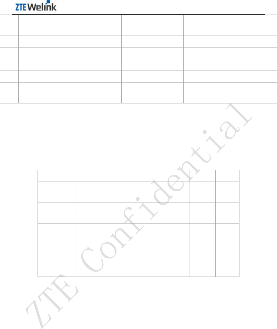
3.5 (U)SIM Card Interface
3.5.1 Description of PINs
ZM5202 WCDMA module baseband processor integrates the (U)SIM card interface
in compliance with ISO 7816-3 standards, and supports to automatically detect
3.0V/1.8V (U)SIM cards. The signals on SIM card interface is as shown in Table
3-5.
Table 3-5 Definition & Description of (U)SIM Card Signal Group
PIN Protocol
Signal
Signal
Definition
Signal Description
48 VREG_RSIM SIM card power Output range: 1.5-3.0V
49 UIM_RST SIM card reset
PIN --
50 UIM_DATA SIM card data
PIN --
51 UIM_CLK SIM card clock
PIN --
52 UIM_DP Data cable
USIM card data signal,
applied on a large-capacity
SIM card
53 UIM_DM Data cable
USIM card data signal,
applied on a large-capacity
SIM card
3.5.2 Electric Feature
On the line close to the (U)SIM card console, be sure to add the ESD circuit
protection during the design.
To comply with the requirements of 3GPP TS 51.010-1 and EMC authentication, it
is recommended to place (U)SIM card console close to the (U)SIM card interface, to
prevent the wiring from being too long, which might seriously distort the waveform
and thus affect the signal integrity. It is recommended to make the grounding
protection for UIM_CLK and UIM_DATA signal wiring. Cascade one 0.1uF and
33pF capacitor between VREG_RSIM and GND, and cascade a 33pF capacitor
Hardware Development Guide of Module Product
18 All Rights reserved, No Spreading abroad without Permission of ZTEWelink
between UIM_CLK, UIM_RST and GND, to filter out the interference by RF signals.
It is recommended to cascade a 20ohm resistance on UIM_DATA cable.
3.5.3 Application of (U)SIM Card Interface
Figure 3-2 (U)SIM Card Signal Connection Circuit
3.6 SD Card Interface
3.6.1 Description of PINs
The SD card interface of ZM5202 module is the storage card based on FLASH,
embedded with 4-bit and 1-bit SD controller, supporting SD and Mini SD cards. Its
PIN signals are as shown in Table 3-6.
Table 3-6 Definition of SD Card Signal Interface
PIN Signal Name Description Function
61 SDCC_DATA0 SD card data cable PIN
SD card data cable
60 SDCC_DATA1 SD card data cable PIN
59 SDCC_DATA2 SD card data cable PIN
58 SDCC_DATA3 SD card data cable PIN
57 SDCC_CLK SD card clock cable PIN SD control clock output
can reach up to 20MHz
56 SDCC_CMD SD card control PIN --
55 VREG_MMC SD card power 3V
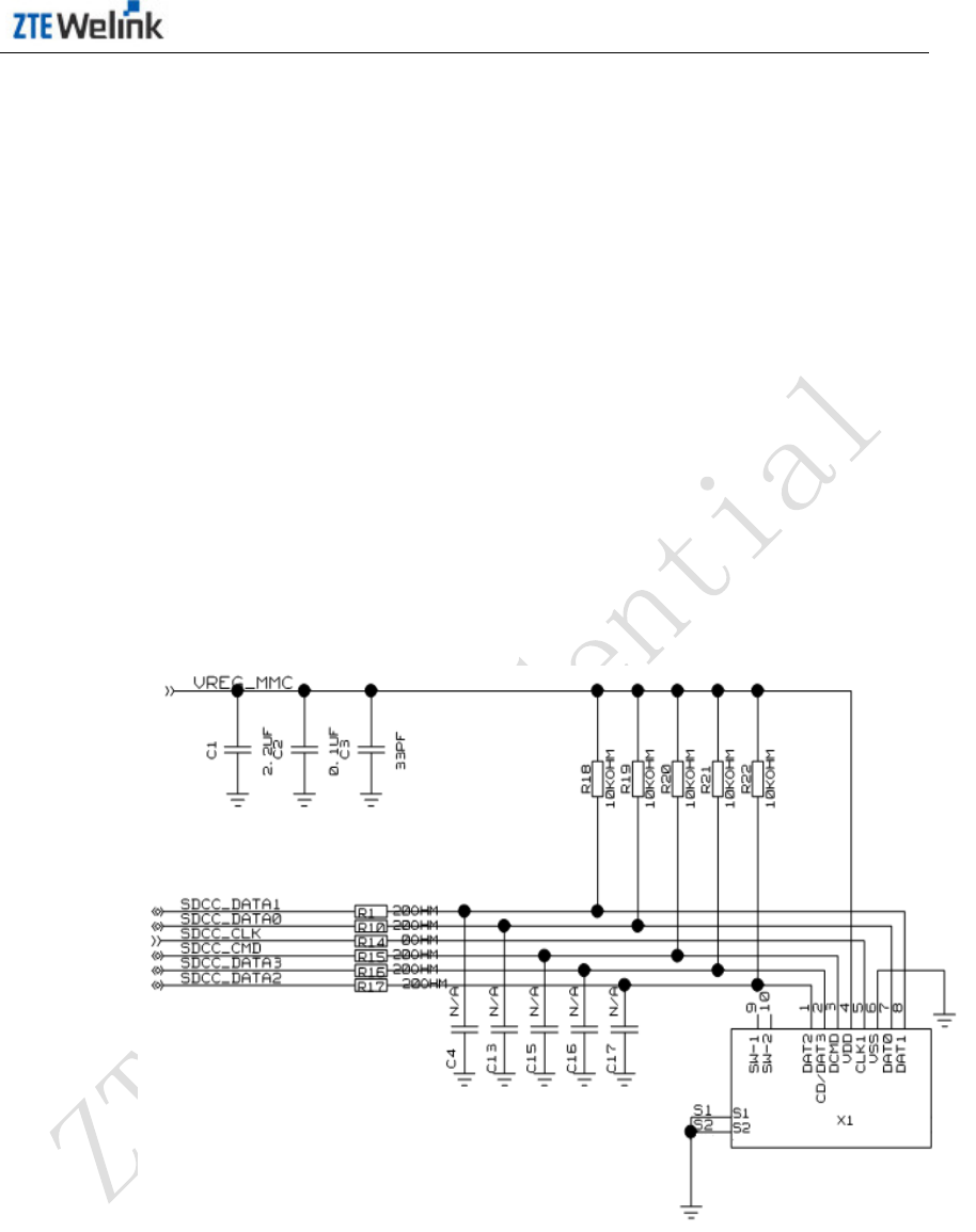
Hardware Development Guide of Module Product
All Rights reserved, No Spreading abroad without Permission of ZTEWelink 19
3.6.2 Electric Feature
SDCC_CLK: Clock signal, host2device, default is 0~25MHz.
SDCC_CMD: Command/response, two-way: the command can sent from the host
to a single card/all cards, the response is sent from a single card/all cards to the
host.
SDCC_DATA[3..0]: Data cable, two-way, default is 0~12.5MB/sec.
3.6.3 Application of SD Card Interface
Figure 3-3 is the reference design diagram for the SD interface. The detection of SD
card adopts the polling mode of DATA3 signal cable to judge whether T card is
inserted or not.
Figure 3-3 SD Typical Application Circuit

Hardware Development Guide of Module Product
20 All Rights reserved, No Spreading abroad without Permission of ZTEWelink
3.7 USB2.0 Interface
3.7.1 Description of PINs
ZM5202 has the high-speed USB2.0 interface, which supports both the full-speed
mode and the high-speed mode. The main processor (AP) is connected with the
module via the USB interface to transmit data.
3.7.2 Electric Feature
The USB interface complies with the USB2.0 specifications and the electric features.
USB_DP, USB_DA are wired strictly according to the differential mode, and the
length difference between the two cables should be restricted within 1mm.
Note: The differential impedance should be controlled within 90ohm.
It is recommended to connect to a high-speed common-mode echo filter on the USB
differential signal wire. If the cable is exposed to the external environment, it is
suggested to add a n ESB protection device. The power capacity of the ESD
protection device should be kept within 1.5pF.
3.7.3 Application of USB Interface
The USB bus is mainly used in data transmission, software upgrading and modular
program detection. Figure 3-4 shows a reference circuit design.
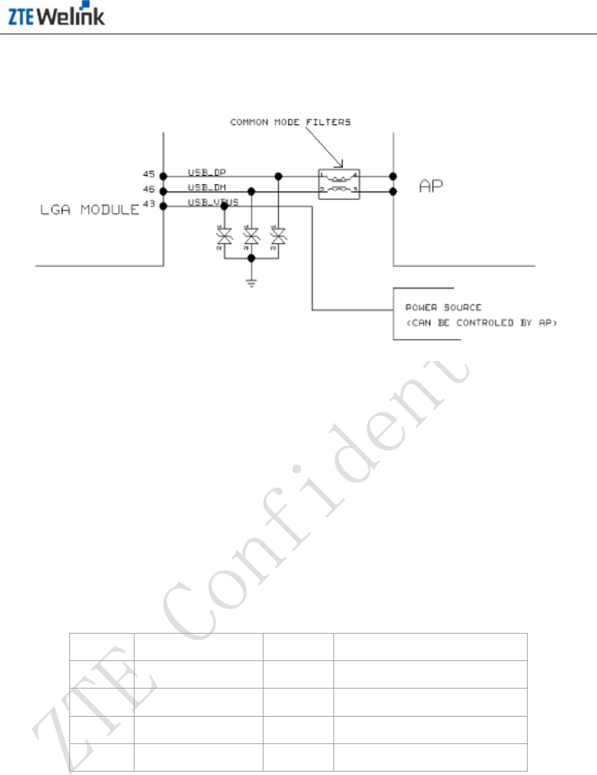
Hardware Development Guide of Module Product
All Rights reserved, No Spreading abroad without Permission of ZTEWelink 21
Figure 3-4 USB Typical Circuit Application
3.8 Serial Interface
3.8.1 SPI (Serial Peripheral Interface) Bus Interface
3.8.1.1 Description of PINs
The definition of SPI interface signaling is defined as shown in Table 3-7.
Table 3-7 Definition of SPI Signal
PIN Signal Name I/O Type Function
39 SPI_ CS_N O SPI segment
40 SPI_ CLK O SPI clock
41 SPI_MISO_DATA B Main input, slave output
42 SPI_MOSI_DATA B Main input, slave output
3.8.1.2 Electric Feature
The SPI bus of ZM5202 is configured as the master equipment, and there are three
modes for SPI:
Running mode: Basic running mode.
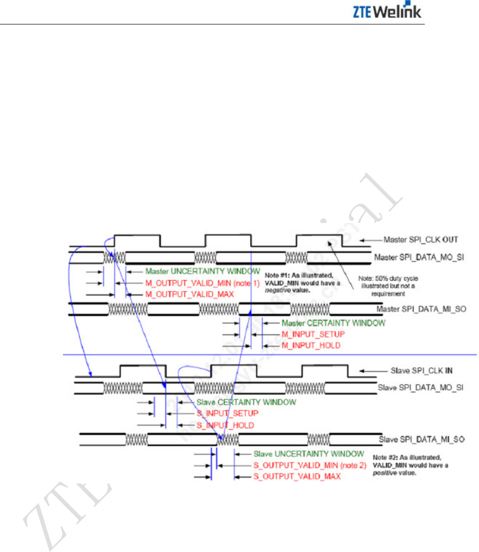
Hardware Development Guide of Module Product
22 All Rights reserved, No Spreading abroad without Permission of ZTEWelink
Waiting mode: The waiting mode of SPI is a configurable low-power mode, enabled
by the byte of the control registered. In the waiting mode, if the waiting byte is
cleared, SPI works under the similar running mode. However, if SPI waits for the
position byte, SPI clock stops and enters the low-power status.
Stop mode: Under the stop mode, SPI is not available, so the power consumption is
reduced. If SPI is configured as the master equipment, any transmission process
will be s topped, but it can enter the running mode when the waiting mode stops.
Figure 3-5 is the SPI bus sequence chart.
Figure 3-5 SPI Bus Sequence Chart
3.8.2 I2C Bus
3.8.2.1 Description of PINs
I2C is the two-wire bus for the communication between ICs, which supports any IC
process (NMOS, CMOS, dual-polarity). The two signal wires, serial data (SDA) and
serial clock (SCL), can transmit information between the connected equipment.
Each equipment is identified by the unique address (such as the micro controller,
storage, LCD driver, audio DAC or keyboard interface). Due to the different
functions of the equipment, it can be used as both the sender and the receiver.
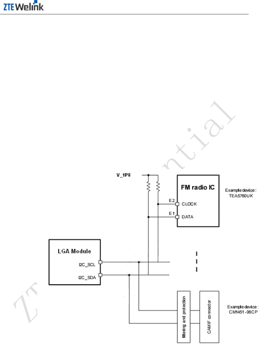
Hardware Development Guide of Module Product
All Rights reserved, No Spreading abroad without Permission of ZTEWelink 23
3.8.2.2 Electric Feature
The I2C interface has the following features:
1. The two-wire bus is used for the communication between ICs.
2. It supports any external equipment of any manufacturing technology (1.8V).
3. It supports the external functions, such as the image sensor, micro controller,
FM radio chip, LCD chip, audio DAC and keyboard interface.
The I2C interface has two working modes with different transmission ratios:
standard mode with a speed as high as 100kbps; high-speed mode with a speed as
high as 400kbps. Figure 3-6 is the I2C reference circuit design diagram.
Figure 3-6 I2C Reference Circuit Diagram
Hardware Development Guide of Module Product
24 All Rights reserved, No Spreading abroad without Permission of ZTEWelink
3.8.3 UART Interface
3.8.3.1 Description of PINs
ZM5202 module provides a circuit of serial communication interface UART, which
complies with the RS-232 interface protocol, and supports the 8-byte serial bus
interface or 2-byte serial interface is Via the UART interface. But the 8-byte serial
bus UART interface and the SPI bus interface are not supported simultaneously.
The module can perform the serial communication and AT instruction interaction
with external.
This UART port supports the programmable data width, programmable data stop
digit and programmable odd/even checksum, and has an independent TX and RX
FIFOs (512 bytes for each). For the normal UART application (non-Bluetooth), the
maximum baud r ate is 230400bps, the 4Mbps high baud rate is only used on
Bluetooth 2.0 application, and the default baud rate is 115200bps. The PINs are
defined as shown in Table 3-8.
Table 3-8 Definition of UART Signal
PIN Signal
Name Description Function
27 UART1_CTS UART port CTS clearing
sending
UART power level
is 1.8V.
28 UART1_RFR UART port RFR preparing to
receive
29 UART1_TXD UART port TXT sending data
30 UART1_RXD UART port RXD data receiving
40 UART_DTR DTE is ready --
41 UART_RI Ring indicator --
42 UART_DSR Data is ready --
39 UART_DCD Carrier detect --
3.8.3.2 Electric Feature
During the software interconnection process, there is a method of capturing logs,
and it is recommended that this interface be kept during the design and the testing
point be reserved. If the module is used together with the application processor, and
the PWL matches with 1.8V, the connection mode is as shown in Figure 3-7. The
Hardware Development Guide of Module Product
All Rights reserved, No Spreading abroad without Permission of ZTEWelink 25
4-wire or 2-wire mode can be us ed for connection. The module interface PWL is
1.8V. If it does not match the PWL of AP interface, it is recommended to add the
PWL conversion circuit.
The connection of ZM5202 UART port and standard RS-232-C interface can be
through the chip like class 232. The design involves the transformation of TTL level
and EIA level. We recommend to use the chip of NLSX5014MUTAG. If using the
2-byte serial bus interface, MAX3232 is recommended, and if using the 8-byte serial
bus interface, SP3238 or MAX3238 is recommended. The connection mode is as
shown in Figure 3-7
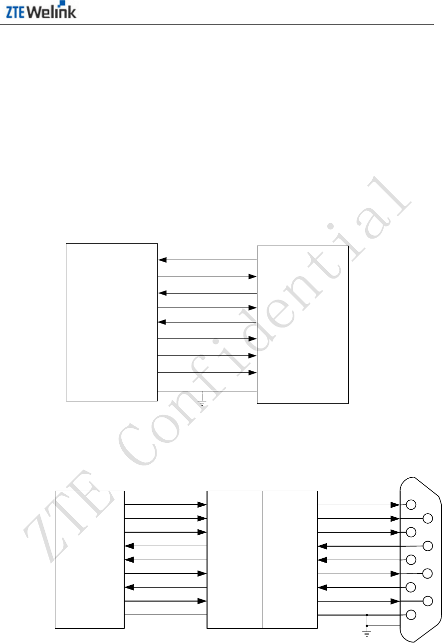
Figure 3-7 Module Serial Port & AP Application Processor
ZM5202 AP
RXD
RXDTXD
TXD
CTS
RFR CTS
RFR
DTR
DSRDSR
DTR
DCD
RI RI
DCD
GND GND
Figure 3-8 The connection of ZM5202 UART and Standard RS-232-C interface
TTL-
RS232
level
translator
SP3238
MAX3238
ZM5202
module
1.8V
-TTL
level
translator
NLSX5014MUTAG
UART_DCD
UART_DSR
UART_TXD
UART_CTS
UART_RXD
UART_RFR
UART_DTR
UART_RI
GND
RS232_DCD
RS232_DSR
RS232_TXD
RS232_CTS
RS232_RXD
RS232_RTS
RS232_DTR
RS232_RI
GND
1
2
3
4
5
6
7
8
9
User Board Female DB9
Note:UART_RFR is equal to UART_RTS.
Hardware Development Guide of Module Product
26 All Rights reserved, No Spreading abroad without Permission of ZTEWelink
3.9 JTAG (Joint Test Action Group) Interface
3.9.1 Description of PINs
The JTAG interface complies with the ANSI/ICEEE Std. 1149.1-1990 standard, and
the interface is defined as shown in Table 3-9.
Table 3-9 Definition of JTAG Signal
PIN Signal Name I/O Type Function
3 JTAG_RESOUT_N DI LGA reset
72 JTAG_TRST_N DI-PD JTAG reset
73 JTAG_RTCK DO JTAG return clock
74 JTAG_TCK DI-PU JTAG clock input
75 JTAG_TDO Z JTAG test data output
76 JTAG_TDI DI-PU JTAG test data input
77 JTAG_TMS DI-PU JTAG test mode
select
78 GND -- Grounding
3.9.2 Application of JTAG Interface
On the system board, you need to reserve the testing point or interface of the
related JTAG signal, so as to solve the un-repairable fault of LGA module due to
emergencies such as downloading interruption.
3.10 Power-on/Power-off & Reset Signal
3.10.1 Description of PINs
The power-on process of ZM5202 module is: Push the POWER_ON PIN for more
than 50ms, pull this PIN upward and then power on. Under the power-on status,
push POWER_ON PIN for more than 5s, then pull this PIN higher, and then power
off. Within the module, POWER_ON PIN is pulled via a 200 K resistance to 1.8V
power. To power on, if it does not need to be powered down, process POWER_ON
according to the figure below.

Hardware Development Guide of Module Product
All Rights reserved, No Spreading abroad without Permission of ZTEWelink 27
Figure 3-9 Module Power-on Plan
PON_RST_N PIN is used to reset the module. After pushing PON_RST_N PIN for
50ms, pull it higher again and then reset the module.
3.10.2 Interface Application
The POWER_ON and PON_RST_N circuits can refer to the design circuit as shown
in Table 3-9. In this figure, the two input signals on t he left are the input control
signals for reset and power-on respectively.
Figure 3-10 Recommended Circuit for Power-on/Power-off & Reset
Hardware Development Guide of Module Product
28 All Rights reserved, No Spreading abroad without Permission of ZTEWelink
3.11 Interactive Application Interface
3.11.1 Description of PINs
Table 3-10 mainly describes the interfaces interacting with the application processor,
including the following three types of interfaces: querying, wakeup and status
indication.
Table 3-10 Interactive Application Interface
PIN Signal Name I/O Type Function
6 AP_READY DI Module querying AP
sleep status
9 MODULE_READY DO AP querying Module
sleep status
10 AP_WAKEUP_MODULE DI AP wakeup Module
11 MODULE
_WAKEUP_AP DO Module wakeup AP
19 MODULE_POWERON DO MODULE power-on
status indication
3.11.2 Interface Application
The ZM5202 module provides 5 handshake signals for the communication with the
application processor (AP). By MODULE_POWERON, AP can query whether LGA
is powered on and is working normally. By MODULE_READY, AP queries whether
the LGA module has entered the sleep status, wakes up the module under the sleep
status by AP_WAKEUP _MODULE. In the same way, when AP is in the sleep
status, the LGA module can query the AP status by AP_READY, and wakes up AP
by MODULE _WAKEUP_AP.
AP_READY: Indicates that the AP server is sleep: the high PWL indicates the sleep
status, and the low PWL indicates the wakeup status.
MODULE_READY: Indicates that the module is sleep: the high PWL indicates the
sleep status, and the low PWL indicates the wakeup status.
AP_WAKEUP_MODULE: After the module has entered the sleep status, the AP
server can wake up the module by the low PWL control; if it’s always on the low
Hardware Development Guide of Module Product
All Rights reserved, No Spreading abroad without Permission of ZTEWelink 29
PWL, the module cannot enter the sleep status. After the AP server enters the high
PWL, the module enters the sleep status.
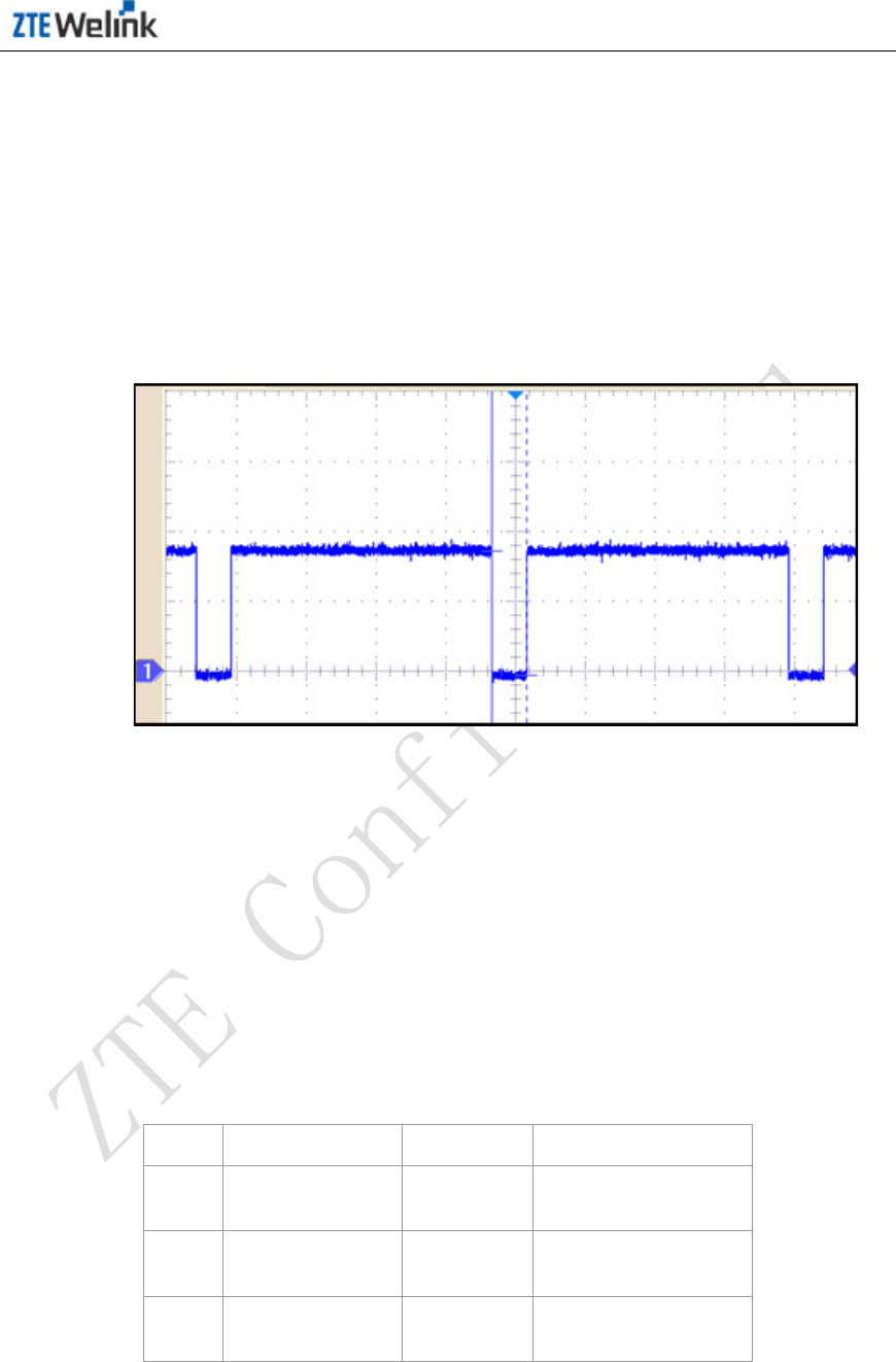
MODULE_WAKEUP_AP: Make sure that the function of remote wake up is enabled
in the config file. When a S MS or call is receiving, the output level of this pin is
shown in the following figure: low for 2s—high for 15s—low for 2s—high for
15s—low for 2s before return its default high level to wakeup the AP side.
Figure 3-11 The output of MODULE_WAKEUP_AP
MODULE_POWERON: After the module is powered on, this signal is set to high,
and kept until the system is restarted or powered down. Low signal indicates that
the server is not powered on, during the power-on process or is being restarted.
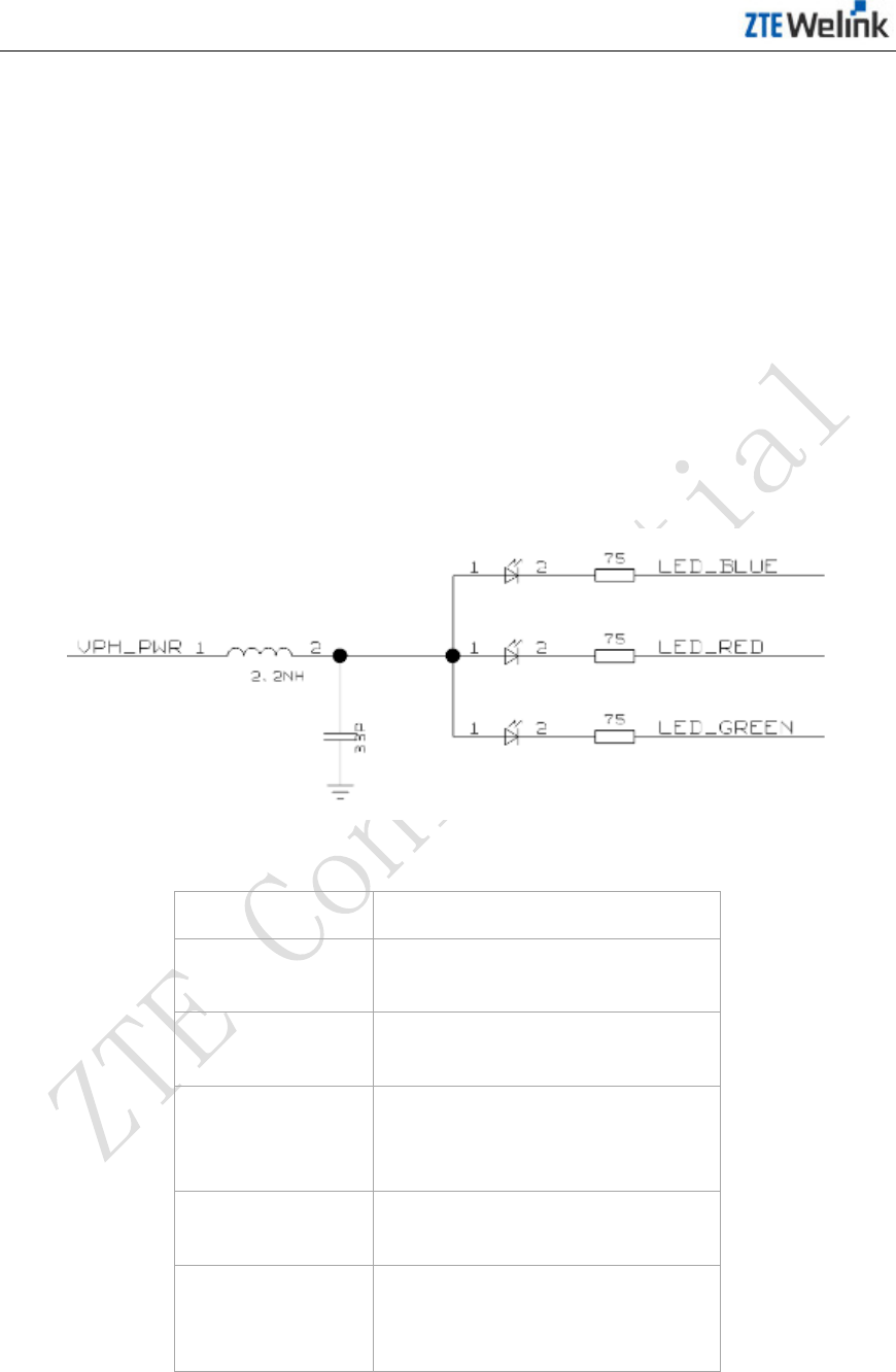
3.12 LED Indicator Interface
3.12.1 Description of PINs
Table 3-11 Definition of LED PIN Signal
PIN Signal Name I/O Type Function
20. LED_GREEN AI Module signal indicator
interface
21. LED_RED AI Module signal indicator
interface
22. LED_BLUE AI Module signal indicator
interface
Hardware Development Guide of Module Product
30 All Rights reserved, No Spreading abroad without Permission of ZTEWelink
3.12.2 Interface Application
The LGA module has three PINs to control the LED indicator, used to indicate the
network connection status. The different modes of status indicator flashing indicate
different network statuses. All the three PINs use the current sink type of current
source for control, which connects to the negative end of LED and connects to
VPH_PWR externally, to directly drive LED. Figure 3-12 is the reference circuit
design diagram. The flashing of indicator is controlled by the switch of RF, and the
LED PIN transmits the control signal to the external. The indicator status is as
defined in Table 3-12. If the RF control is not needed, the AP server can design the
status of control indicator by itself.
Figure 3-12 Reference Circuit of Status Indicator
Table 3-12 Definition of Indicator Status
Indicator Status Module Working Status
RED indicator
always on Not registered to the network
GREEN indicator
always on
Have been registered to 2G
network
GREEN indicator
flashing
Have been registered to 2G
network, and there is data service
as well.
BLUE indicator
always on
Have been registered to 3G
network
BLUE indicator
flashing
Have been registered to 3G
network, and there is data service
as well.
Hardware Development Guide of Module Product
All Rights reserved, No Spreading abroad without Permission of ZTEWelink 31
4 Electric Feature
4.1 Power Feature
4.1.1 Power Supply
The input voltage range of ZM5202 is DC 3.4V~4.2V, and the typical value is 3.8V,
as shown in Table 4-1.
Table 4-1 Input Voltage
Parameter Min Typical Max
Input
voltage
3.4V 3.8V 4.2V
4.1.2 Working Current
The working current range of ZM5202 is as shown in Table 4-2. The IDLE mode
indicates the power consumption of the module when there is no service. The table
also provides the working current range under GSM and WCMA mode when there
is data service.
Table 4-2 Working Current
Mode Status Average Remark
GSM With no service ≤75mA IDLE mode
With data
transmission
≤380mA GPRS/EDGE
mode
WCDMA With no service ≤75mA IDLE mode
With data
transmission
≤470mA HSPA mode
Note: The above average current is acquired under the maximum transmission power. Under different
environments, the testing results might be slightly different. Take the actual situation as the reference.

Hardware Development Guide of Module Product
32 All Rights reserved, No Spreading abroad without Permission of ZTEWelink
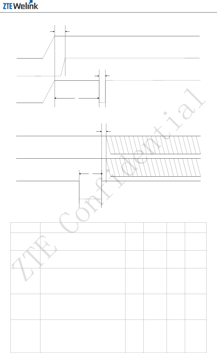
4.2 Power-on/Power-off Flow
To guarantee the user can power on and power off stably, you can refer to the
power-on sequence chart as shown in Figure 4-1 and the power-off sequence chart
as shown in Figure 4-2. Table 4-3 shows the power-on and resetting time, which
needs to be paid attention to during the module power-on process.
1. Once VPH_PWR is powered on, the POWER_ON signal will be synchronized
and be established as the high PWL.
2. After VPH_PWR is established normally, the interval between it to the
POWER_ON signal cannot be too short. Refer to T2 parameter. ZTEWelink
recommends that VPH_PWR adopt the power-off plan that does not
disconnect the power supply.
3. The power-on startup time takes the lower level of POWER_ON as the starting
point, and POWER_ON needs to be released after being kept on the low PWL
for a period.
4. SUB_VBUS is the USB PHY power supply. It is not recommended to be
established before VPH_PWR.
During the process of establishing the module PINs, pay attention to the following
items:
1. To power off by the POWER_ON signal, the T4 period needs to be designed
as required.
2. After VPH_PWR and USB_VBUS are powered off, it is recommended not to
disconnect the power supply.
Hardware Development Guide of Module Product
All Rights reserved, No Spreading abroad without Permission of ZTEWelink 33
Figure 4-1 Power-on Sequence Chart of ZM5202 Module
VPH_PWR
USB_VBUS
POWER_ON
T1
T2
T3
Figure 4-2 Power-off Sequence Chart of ZM5202 Module
POWER_ON
T5
T4
VPH_PWR
USB_VBUS
Table 4-3 Power-on/Power-off Time
Parameter Description Min Typical Max Unit
T1 From powering on VPH_PWR to
establishing USB_VBUS
0 0.5 1 second
T2 From powering on VPH_PWR to
Power-on taking effect
1 1.5 -- second
T3 The period that the Power-on signal
for power on operation is kept on
the low PWL
0.05 0.1 -- second
T4 The period that the Power-on signal
for power off operation is kept on
the low PWL
4 5 -- second
T5 From the releasing the Power-on
button for power off operation to the
power off of VPH_PWR and
USB_VBUS
1 2 -- second
Hardware Development Guide of Module Product
34 All Rights reserved, No Spreading abroad without Permission of ZTEWelink
4.3 Resetting Flow
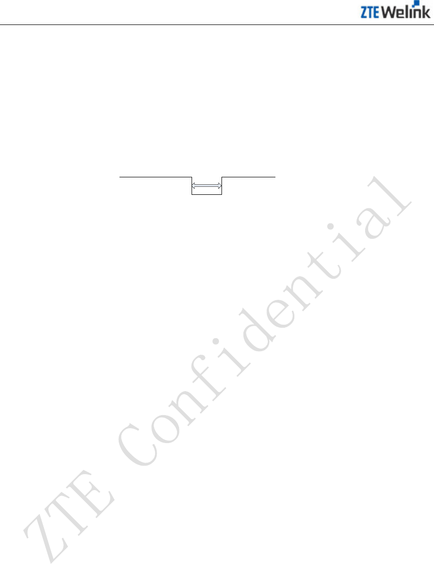
The PON_RST_N reset signal of ZM5202 module is the increasing resetting, so it is
reset after decreasing this PIN by 100ms. Figure 4-3 is the module resetting flow.
Figure 4-3 Module Resetting Flow
100ms
1
0
PON_RST_N

Hardware Development Guide of Module Product
All Rights reserved, No Spreading abroad without Permission of ZTEWelink 35
5 Technical Index of Radio Frequency
5.1 Technical Index of Radio Frequency under
UMTS Mode
5.1.1 UMTS (WCDMA)
The RF index should be tested strictly in accordance with the related testing
specifications of 3GPP. The RF indexes of UMTS2100/1900/850 should satisfy the
requirements of 3GPP TS 34.121 protocol.
5.2 Technical Index of Radio Frequency under
GPRS/GSM/EDGE Mode
The RF indexes of GSM/GPRS/EDGE850/900/1800/1900 should satisfy the
requirements of 3GPP TS 05.05 protocol.
5.3 Technical Parameters of Antenna Testing
Console
ZM5202 supports the AGPS function, so the system equipment needs to add the
AGPS antennal. The design of AGPS antenna is consistent with that of the main
antenna, and its efficiency index can be 3dB lower. The separation degree between
the main antenna and the diversity antenna is required to be greater than 12dB. The
antenna index is divided into the sourceless index and s ourced index. The
sourceless index includes S11, efficiency, gains, orientation diagram and polarity,
which can be used as the parameter measuring the performance of the antenna
itself. The sourced index is also called the OTA index, including TRP (all-round
radiation power), TIS (all-round receiving sensitivity), radiation orientation diagram,
which is an important index measuring the radiation performance of the whole set
(including the antenna, module, circuit main board).
Hardware Development Guide of Module Product
36 All Rights reserved, No Spreading abroad without Permission of ZTEWelink
5.3.1 Sourceless Index
The sourceless indexes of antenna are different according to the different
requirements of wireless Internet products. Here, taking the 3G Internet notepad as
an example, the sourceless index of the antenna is recommended to reach the
standards as described below.
Table 5-1 Sourceless Index of Main Antenna (Recommended)
Frequency Band 824-960MHz 1710-2170MHz
VSWR in Free Space <3:1 <3:1
Peak Gain in Free Space >0dBi >0dBi
3-D Average Gain in Free
Space -3dBi -3dBi
Antenna Efficiency >50% >50%
5.3.2 Sourced Index
The sourced indexes of antenna are different according to the different
requirements of the product type. Here, taking the 3G Internet notepad as an
example, the sourced index of the antenna is recommended as below.
TRP: <W850/W900/W1900/W2100>18dBm;
GSM850>27dBm, GSM900>27dBm;
DCS1800>24dBm, PCS1900>24dBm>;
TIS: <W850/W900<-100dBm; W1900/W2100<-103dBm;
GSM850<-100dBm, GSM900<-100dBm;
DCS1800/PCS1900<-102dBm.
Hardware Development Guide of Module Product
All Rights reserved, No Spreading abroad without Permission of ZTEWelink 37
6 Related Test & Testing Standard
6.1 Testing Reference
The related tests of ZM5202 comply with the IEC standard, including the equipment
running under high/low temperature, storage under high/low temperature,
temperature shock and EMC. Table 6-1 is the list of testing standard, which includes
the related testing standards for ZM5202.
Table 6-1 Testing Standard
Testing
Standard
Document Reference
IEC6006826 Environmental testing-Part2.6:Test FC: Sinusoidal Vibration
IEC60068234 Basic environment testing procedures part2.
IEC60068264 Environmental testing-part2-64: Test FH: vibration, broadband
random and guidance.
IEC60068214 Environmental testing-part 2-14: Test N:change of
temperature.
IEC60068229 Basic environmental testing procedures-part2: Test EB and
guidance.
IEC6006822 Environmental testing-part2-2:Test B:dry heat
IEC6006821 Environment testing-part2-1: Test A: cold.
GB/T 15844.2 MS telecommunication RF wireless phone-set environment
requirement & experimental method – part 4: Strict level of
experimental condition
GB/T 2423.17 Basic environment experiment of electronic
products-Experiment Ka: Salt mist experiment method
GB/T 2423.5 Basic environment experiment of electronic
products-Part2:Experiment method Try Ea & Introduction:
Shock
GB/T 2423.11 Basic environment experiment of electronic
products-Part2:Experiment method Try Fd: Broad frequency
band random vibration (General requirement)
TIA/EIA 603 3.3.5 TIA Standard-part3-5:Shock Stability
Note: 1. IECL International Electro technical Commission; 2. GB/T: Recommended national standard
Hardware Development Guide of Module Product
38 All Rights reserved, No Spreading abroad without Permission of ZTEWelink
6.2 Description of Testing Environment
The working temperature range of ZM5202 is divided into the normal working
temperature range and the extreme working temperature range. Under the normal
working temperature range, the testing result of RF complies with the requirements
of 3GPP specifications, and its function is normal. Under the extreme temperature
range, the RF index basically complies with the 3GPP specifications, and the quality
of data communication is affected to a certain extent, but its normal function is not
affected. ZM5202 has passed the EMC test. Table 6-2 is the requirement for the
testing environment, and Table 6-3 lists out the instruments and devices that might
be used during the test.
Table 6-2 Testing Environment
Working
Condition
Min
Temperature
Max
Temperature
Remark
Normal
working
condition
-20°C 75°C All the
indexes are
good.
Extreme
working
condition
-40°C 85°C Some
indexes
become
poorer.
Storage -40°C 85°C Storage
environment
of ZM5202
Table 6-3 Testing Instrument & Device
Testing Item Instrument & Device
RF test Comprehensive
testing device
RF cable
Tower antenna
Microwave darkroom
High/Low-temperature
running & storage test
High/Low-temperature
experimental box
Temperature shock
test
Temperature shock
experimental box
Vibration test Vibration console
Hardware Development Guide of Module Product
All Rights reserved, No Spreading abroad without Permission of ZTEWelink 39
6.3 Reliability Testing Environment
The reliability test includes the vibration test, high/low-temperature running,
high/low-temperature storage and temperature shock experiment test. Refer to
Table 6-4 for the specific parameters.
Table 6-4 Reliability Features
Testing Item Testing Condition Testing
Standard
Random
vibration
Frequency range: 5-20Hz,
PSD:1.0m2/s3
Frequency range: 20-200Hz,
-3dB/oct
3 axis, 1 hour for each axis
IEC 68-2-6
Temperature
shock
Low temperature: -40°C ±2°C
High temperature: +80°C ±2°C
Temperature changing period: less
than 30seconds
Test duration: 2 hours
Cycle: 10
IEC 68-2-14 Na
High-temperature
running
Normal high temperature: 75 °C
Extreme high temperature: 85°C
Duration: 24 hours
ZTE standard
Low-temperature
running
Normal low temperature: -20°C
Extreme low temperature: -40°C
Duration: 24 hours
ZTE standard
High temperature
& high humidity
Temperature: +60°C
Humidity: 95%
Duration: 48 hours
ZTE standard
High temperature
storage:
Temperature: 85°C
Duration: 24 hours
IEC 68-2-1 Ab
Low temperature
storage:
Temperature: -40°C
Duration: 24 hours
IEC 68-2-2 Bb
Hardware Development Guide of Module Product
40 All Rights reserved, No Spreading abroad without Permission of ZTEWelink
6.4 Reliability Testing Result
Table 6-5 Temperature Testing Result Under Windless Environment
Mode Temperature Voltage Transmission
Power
Duration Testing
Result
GPRS
Class 10
+25 ℃ (3.8±10%)V Max ≥1hour Pass
EDGE
Class 12
+25 ℃ (3.8±10%)V Max ≥1 hour Pass
WCDMA +25 ℃ (3.8±10%)V Max ≥1 hour Pass
Table 6-6 High/Low-temperature Running & Storage Testing Result
Testing Item Testing
Condition &
Standard
Testing Content Testing
Result
Random
vibration
Refer to Table 6-4 RF test & function
test
Pass
Temperature
shock
Refer to Table 6-4 RF test & function
test
Pass
Low-temperature
working
Refer to Table 6-4 RF test & function
test
Pass
High-temperature
working
Refer to Table 6-4 RF test & function
test
Pass
Extreme
low-temperature
working
Refer to Table 6-4 RF test & function
test
Pass
Extreme
high-temperature
working
Refer to Table 6-4 RF test & function
test
Pass
Low-temperature
storage
Refer to Table 6-4 RF test & function
test
Pass
High-temperature
storage
Refer to Table 6-4 RF test & function
test
Pass

Hardware Development Guide of Module Product
All Rights reserved, No Spreading abroad without Permission of ZTEWelink 41
7 Design Guide
This chapter provides the general design guide for ZM5202, used as a reference for
the user during the design process, so that the product can reach better
performance.
7.1 General Design Rule & Requirement
When the user is designing the peripheral circuits of ZM5202, he needs to first
guarantee that the external circuit has the sufficient power supply capability, and the
USB of high-speed signal cable is required to have 90ohm differential resistance.
For the common signal interface, it is required to design according to ZTEWelink
requirements, which needs to comply with the power level of interface signal, so as
to prevent the impedance from damaging the module. The RF index of this product
itself is good, and the user needs to design the antenna circuit of the main board
and make the corresponding impedance control. Otherwise, the RF index of the
whole set will be affected.
7.2 Power Supply Circuit Design
It is required that the power supply capability of VPH_PWR on the system board
reach 2.5A or above, so as to satisfy the requirement of peak current on the module.
And the average current of the power on the system side should also reach 0.9A or
above. The power cable on the system board should be thick enough, and should
form a good reflux with the ground. Besides, in the power supply circuit design, the
user needs to add the large storage capacitor on the kilo level, to guarantee the
transient power supply capability.
Hardware Development Guide of Module Product
42 All Rights reserved, No Spreading abroad without Permission of ZTEWelink
7.3 RF Circuit Design
7.3.1 RF Antenna Circuit Design
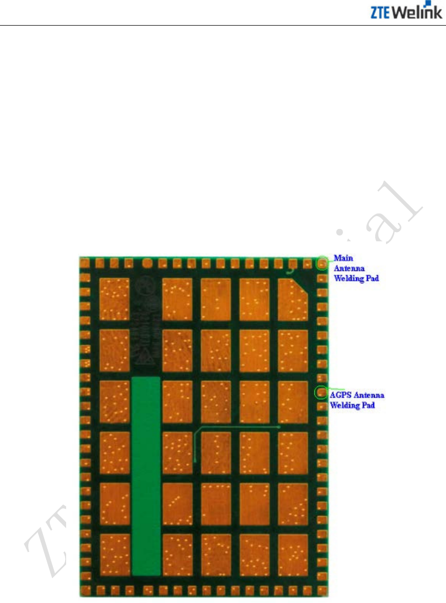
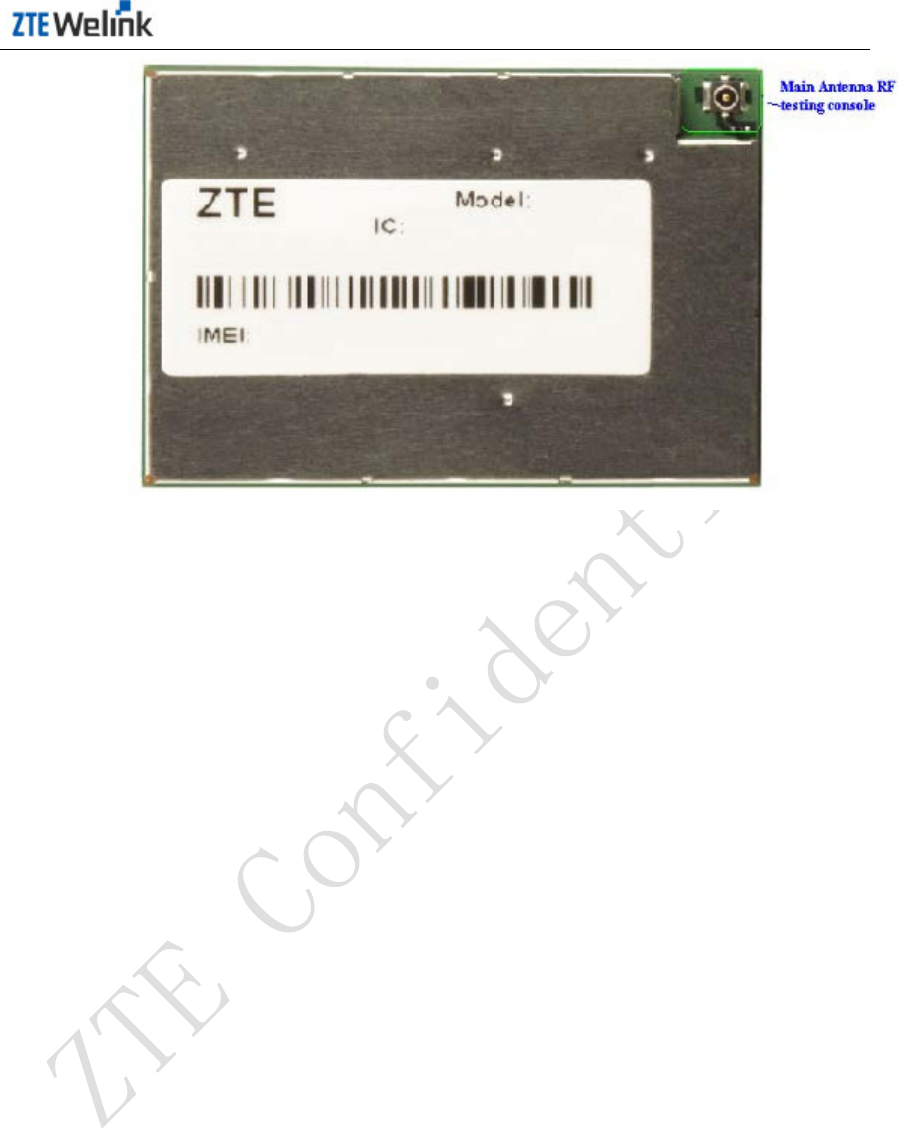
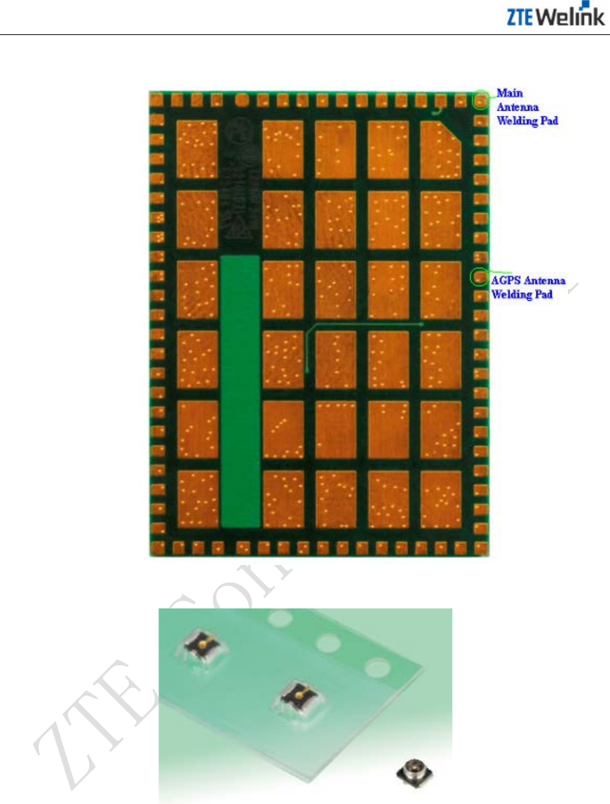
There are two interfaces on the RF antenna of ZM5202: main antenna interface,
and GPS antenna. The main antenna supports two access modes of RF signal: by
PDA wielding panel mode and by RF connector mode. The GPS antenna only
supports the access mode of LGA wielding panel. Figure 7-1 is the main antenna
connector interface, and Figure 7-2 Interface of Main Antenna and AGPS Antenna
Welding Pad
Figure 7-3 shows the interface between the antenna and the GPS antenna.
Currently, ZTEWelink adopts the W.FL-R-SMT-1 RF connector testing console from
HRS company, as shown in
Figure 7-1 Main Antenna RF Connector Interface
Hardware Development Guide of Module Product
All Rights reserved, No Spreading abroad without Permission of ZTEWelink 43
Hardware Development Guide of Module Product
44 All Rights reserved, No Spreading abroad without Permission of ZTEWelink
Figure 7-2 Interface of Main Antenna and AGPS Antenna Welding Pad
Figure 7-3 RF Interface Testing Console (W.FL-R-SMT-1 from HRS)
If the main antenna is access by the RF connector, the corresponding cables of RF
interface are recommended to use the W.FL-LP-04N of HRS company, as shown in
Figure 7-4. When this connection mode is adopted, the antenna RF connector can
be directly inserted to the RF testing console of the module, so it saves the
connection between the RF port and the antenna interface.
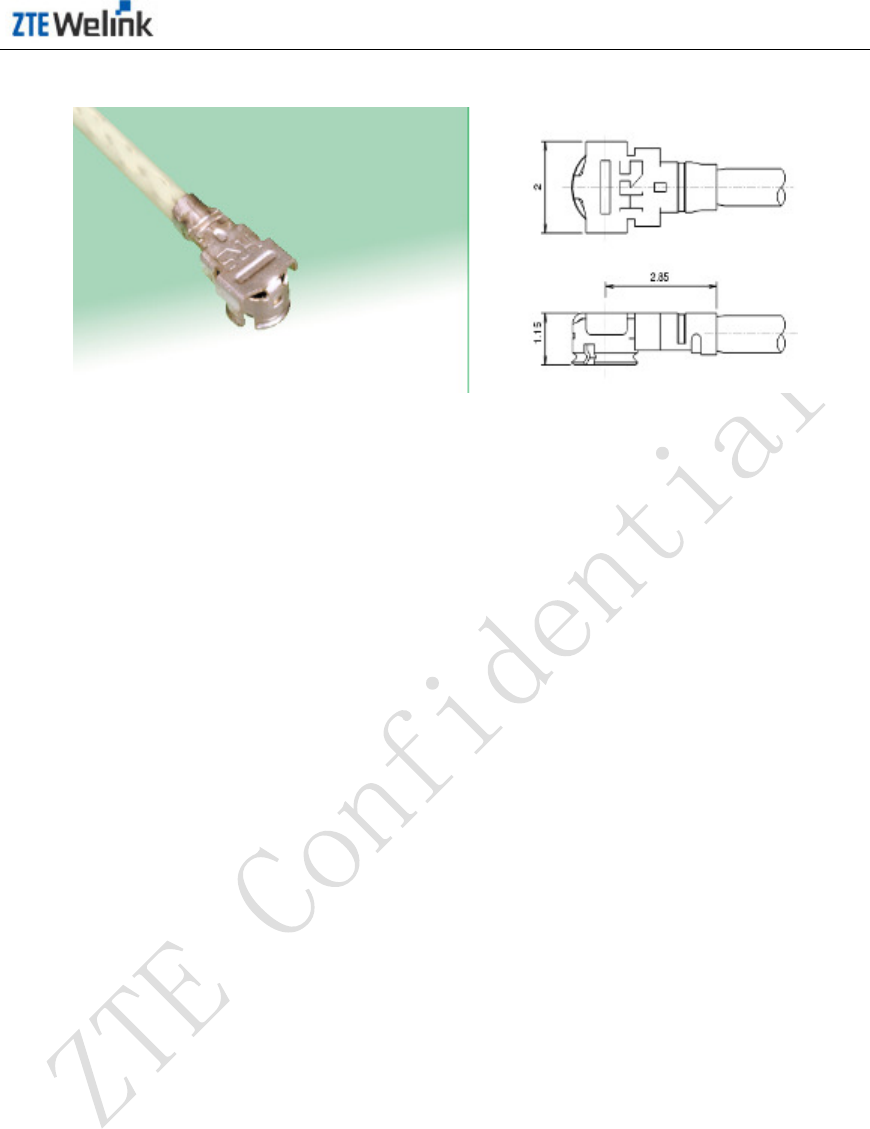
Hardware Development Guide of Module Product
All Rights reserved, No Spreading abroad without Permission of ZTEWelink 45
Figure 7-4 Testing Cable
If the main antenna is accessed by the PDA wielding panel, the RF main antenna
wield pane of the module itself needs to be connected to the antenna interface on
main board via the wield pane and micro stripline or stripline. The micro stripline or
stripline is designed according to the 50ohm impedance, and the dual-L model
matching circuit is reserved.
For the different terminal products, the dimensions are different, the requirements
for the antenna performance are different, so the size and location of antenna are
different as well. Taking the 3G Internet notepad as an example, its antenna space
is recommended to be above 7mm*10mm*100mm, and be placed above the top of
LCD screen.
The design of AGPS antenna is consistent with the main antenna, and its efficiency
index is allowed to be 3dB lower. The separation degree between the main antenna
and the diversity antenna is required to be greater than 12dB.
7.3.2 Precautions During the Initial Design of Antenna
7.3.2.1 Preliminary Evaluation
When choosing the antenna position, make sure that the antenna and the base
station are kept on the horizontal level, so as to reach the highest efficiency. Then,
avoid the place the antenna close to the switch power or data cable, chip or another
device that might result in electromagnetic interference. Place the antenna in a
location that the hand cannot reach, to prevent from the attenuation generated by
the body. Also take into consideration the reduction of radiation and the feasibility of

Hardware Development Guide of Module Product
46 All Rights reserved, No Spreading abroad without Permission of ZTEWelink
its structure. Therefore, during the initial design, make the layout evaluation with the
structure, ID, circuit and antenna engineers together.
7.3.2.2 Suggested Antenna Location
For the notepad, the ideal location position for the antenna is on the left corner or
right corner of LCD, because this position is relatively far away from the main board,
so the electromagnetic interface is little. Besides, this position is relatively far away
from the human body, so the SAR index can be easily satisfied. Another suggested
position is on the left or right of LCD. For the other products such as the router or
electronic book, make the evaluation according to the feature of the product itself.
7.3.2.3 Suggested Antenna Occupancy Space
As different antenna manufacturers might adopt different antenna modes, the
reserved space of the antenna is also different. Taking the 3G Internet laptop as an
example (coverage frequency: W2100/W1900/W900/W850, GSM850/GSM900/
GSM1800/GSM1900), it is recommended to set the antenna size as 5mm (width) *
12mm (width) * 80mm (length).
7.3.2.4 Main Board Layout
The interference on the main board area is very strong. According to the testing
result, when the module is placed in these interference areas, its performance
becomes poorer. When designing the notepad, it’s better to separate the module
form the main board PCB, instead of installing the module on the main board. If they
are not separated, the module should better be far away from the chip, storage,
power interface, data cable interface and other module or device that might
generate EMI.
7.3.2.5 Antenna RF Connection Cable
The RF connection cable of the antenna should better be short. Taking
consideration of the transmission power los, it is recommended to adopt a thicker
RF cable. At the same time, the RF cable should better be far away from FSB, chip
and storage, power interface, data cable interface, and other modules or devices
that might generate EMI. The connection antenna and the RF connection cable of

Hardware Development Guide of Module Product
All Rights reserved, No Spreading abroad without Permission of ZTEWelink 47
3G module cannot go on the right angle, cannot be crushed or worn. The RF cable
should better be wired close to the ground of main board.
7.3.2.6 Matching Circuit of Antenna
If the module RF interface needs to be transferred with the antenna interface, when
designing the main board circuit, the micro stripline or stripline between the module
RF testing console and the antenna interface RF testing console should be
designed by the 50ohm impedance, and the dual-L model matching circuit is
reserved. If the antenna RF connector is directly inserted to the module RF testing
console, the transfer between the module RF port and the antenna interface can be
saved.
7.3.2.7 Type of Antenna RF Cable & RF Connector
The antenna RF connection cable usually adopts GBE(TW) and Shenyu (Mainland),
or Japanese Somitomo and Shin Din. The antenna RF cable usually adopts a line
width of 1.37mm. The antenna RF connector usually adopts Japanese IPX, or HRS,
while the price of the latter is higher.
7.4 Suggestions for EMC & ESD Design
During the design of the whole set, the user needs to fully consider the EMC
problem caused by the signal integrity and power integrity. During the layout and
wiring of peripheral circuits, for the wiring of power and signal cables, keep a
distance of 2 t imes of the line width, so as to effectively reduce the coupling
between signals and keep a clean reflux path for the signal. During the design of
peripheral power circuits, the de-coupled capacitor should be placed closed to the
module power PIN, the high-frequency high-speed circuit and the sensitive circuit
should be placed far away from the border of PCB. They should better be separated
during layout, so as to reduce the interference between them and protect the
sensitive signal. For the circuit or device on the side of system board that might
interfere the module, it should be shielded during design.
ZM5202 is embedded on the side of system board, so the user needs to make the
ESD protection during design. For the key input/output signal interface, such as the

Hardware Development Guide of Module Product
48 All Rights reserved, No Spreading abroad without Permission of ZTEWelink
(U)SIM card signal interface, the ESD device should be placed closely for protection.
Besides, on the side of main board, the user should reasonably design the structure
and PCB layout, guarantee that the metallic shielding shell is fully grounded, so as
to leave a smooth discharge channel for ESD.
7.5 Suggestions for PCB Wielding Panel Design
When the user is designing the encapsulation wielding panel on main board, the 30
heat wielding panels in the center are recommended to be designed according to
the dimensions as described in Figure 2-1. The surrounding 78 wielding panels
should be extended by more than 0.3mm, and the other three sides of the wielding
panel are extended by 0.05mm. For the right angles of wielding panels for the main
antenna PIN1 and A GPS antenna PIN70, they are recommended to be r ounded
into a round angel with a radius of 0.3mm. In this way, it is convenient for the import
of interference and the radiation of RF signal.
7.6 Suggestions for Heat-dissipation Design
The module will dissipate heat during the working process, and might also be
affected by other high-temperature devices. The heat dissipation is taken into full
consideration during the product design, as 30 heat wielding panels are reserved in
the center of the module. During the connection with the system board, make sure
that these wielding panes are grounded well, which is greatly helpful to heat
conductivity and heat balance, and is greatly beneficial to the electric performance
of the whole set as well.
Note:
1. Keep this product away from heat-dissipation devices with high power, to
prevent the temperature of the module from being too high. .
2. Do not put the module close to the large heat-dissipation devices, such as
CPU or bridge. The high temperature will affect the RF performance.

Hardware Development Guide of Module Product
All Rights reserved, No Spreading abroad without Permission of ZTEWelink 49
7.7 Recommended Product Upgrading Plan
It’s recommended to use the one-click software upgrade tool to upgrade through the
USB port provided by ZTEWelink in the Windows system. If the customer wants to
upgrade the module in other operation systems, ZTEWelink provides the
corresponding reliable tools too.
Hardware Development Guide of Module Product
50 All Rights reserved, No Spreading abroad without Permission of ZTEWelink
8 Manufacturing Guide
8.1 Design of Steel Mesh
During the design of steel mesh, note:
1. When manufacturing the steel mesh of thermal pad on the bottom of the
module, narrow the mouth of the steel mesh to 75% of the original size, so as
to reduce the risk of shortcut between the module thermal and the peripheral
PINs. This method is effective.
2. It is recommended to design to the mouth of steel mesh on the thermal pad
wielding panel to the lattice form. Figure 8-1 shows the recommended pattern
for the steel mesh.
Figure 8-1 Recommended Pattern of Steel Mesh on Wielding panel
8.2 Furnace Temperature Curve
The furnace temperature curve greatly affects the wielding quality and the material
status, so it needs to be paid great attention to. The temperature increasing speed
cannot be too fast, with the increase speed from the room temperature to 150℃
less than 3℃/second. At the same time, if the temperature is above 217℃, the
duration should be kept within 70 seconds, while the interim value 55 seconds is
ideal. Otherwise, the great temperature shock will make certain devices ineffective,
causing the quality to decrease and the maintenance difficulty to increase. At the
same, keep the precise maximum temperature to be below 245℃, as certain
materials (such as the crystal) might crack under the high temperature and won’t not
vibrate any more, so the product function is affected. Refer to Table 8-1 for the
setting of furnace temperature curve, refer to Figure 8-2 for the furnace temperature

Hardware Development Guide of Module Product
All Rights reserved, No Spreading abroad without Permission of ZTEWelink 51
curve, and refer to Figure 8-3 for the testing result. Figure 8-2 and Figure 8-3 are
only a reference, and refer to Table 8-1 for the detailed requirements.
9 FCC Regulations:
This device complies with part 15 of the FCC Rules. Operation is subject to the following two conditions: (1)
This device may not cause harmful interference, and (2) this device must accept any interference received,
including interference that may cause undesired operation.
Changes or modifications not expressly approved by the party responsible for compliance could void the
user‘s authority to operate the equipment.
This device has been tested and found to comply with the limits for a Class B digital device , pursuant to Part
15 of the FCC Rules. These limits are designed to provide reasonable protection against harmful interference
in a residential installation. This equipment generates, uses and can radiated radio frequency energy and, if
not installed and used in accordance with the instructions, may cause harmful interference to radio
communications. However, there is no guarantee that interference will not occur in a particular installation If
this equipment does cause harmful interference to radio or television reception, which can be determined by
turning the equipment off and on, the user is encouraged to try to correct the interference by one or more of
the following measures:
-Reorient or relocate the receiving antenna.
-Increase the separation between the equipment and receiver.
-Connect the equipment into an outlet on a circuit different from that to which the receiver is connected.
-Consult the dealer or an experienced radio/TV technician for help.
Caution: Changes or modifications not expressly approved by the party responsible for compliance could void
the user‘s authority to operate the equipment.
RF Exposure Information
This device complies with FCC radiation exposure limits set forth for an uncontrolled environment. In order to
avoid the possibility of exceeding the FCC radio frequency exposure limits, human proximity to the antenna
shall not be less than 20cm (8 inches) during normal operation.
IMPORTANT NOTE
This module is intended for OEM integrator. The OEM integrator is still responsible for the FCC compliance
requirement of the end product, which integrates this module. 20cm minimum distance has to be able to be
maintained between the antenna and the users for the host this module is integrated into. Under such
configuration, the FCC radiation exposure limits set forth for an population/uncontrolled environment can be
satisfied.

Hardware Development Guide of Module Product
52 All Rights reserved, No Spreading abroad without Permission of ZTEWelink
Any changes or modifications not expressly approved by the manufacturer could void the user's authority to
operate this equipment.
USERS MANUAL OF THE END PRODUCT:
In the users manual of the end product, the end user has to be informed to keep at least 20cm separation
with the antenna while this end product is installed and operated. The end user has to be informed that the
FCC radio-frequency exposure guidelines for an uncontrolled environment can be satisfied. The end user has
to also be informed that any changes or modifications not expressly approved by the manufacturer could void
the
user's authority to operate this equipment. If the size of the end product is smaller than 8x10cm, then
additional FCC part 15.19 statement is required to be available in the users manual: This device complies
with Part 15 of FCC rules. Operation is subject to the following two conditions: (1) this device may not cause
harmful interference and (2) this device must accept any interference received, including interference that
may cause undesired operation.
LABEL OF THE END PRODUCT:
The final end product must be labeled in a visible area with the following " Contains TX FCC ID:
SRQ-ZM5202". If the size of the end product is larger than 8x10cm, then the following FCC part 15.19
statement has to also be
available on the label: This device complies with Part 15 of FCC rules.
Operation is subject to the following two conditions: (1) this device may not cause harmful interference and (2)
this device must accept any interference received, including interference that may cause undesired
operation.
Table 8-1 Curve Temperature Curve Parameter Setting
Lead-free Curve Temperature Curve
Phase Temperature Duration
Pre-heat Temperature is
increased from room
temperature to 150℃
Temperature
increasing ratio
<3℃/second
Temperature
keeping
150℃~200℃ 40~110
seconds
Wielding Greater than 217℃ 40~70 seconds
Above 230℃ 15~45 seconds
Peak temperature MAX: 245℃
MIN: 230℃
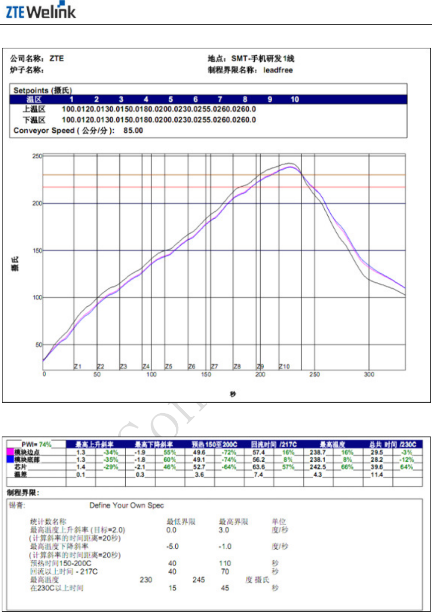
Hardware Development Guide of Module Product
All Rights reserved, No Spreading abroad without Permission of ZTEWelink 53
Figure 8-1 Furnace Temperature Curve Reference Diagram
Figure 8-2 Testing Result