ZTE ZTEMC2261 CDMA 1X Module User Manual
ZTE Corporation CDMA 1X Module Users Manual
UserManual.wiki
>
ZTE
>
ZTEMC2261 User Manual
Users Manual
Navigation menu
Upload a User Manual
Namespaces
Wiki Guide
HTML
PDF
Info
Views
User Manual
Discussion / Help
Navigation

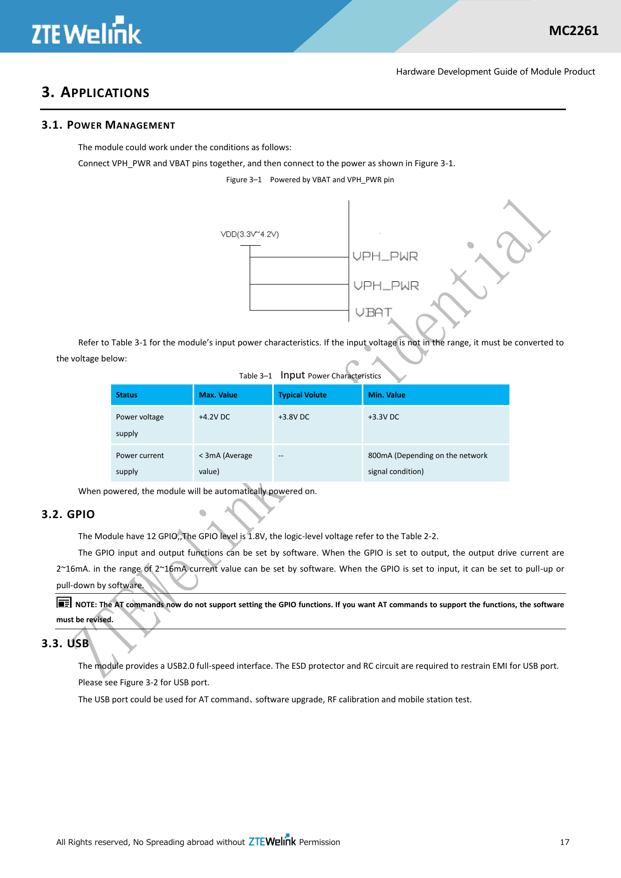
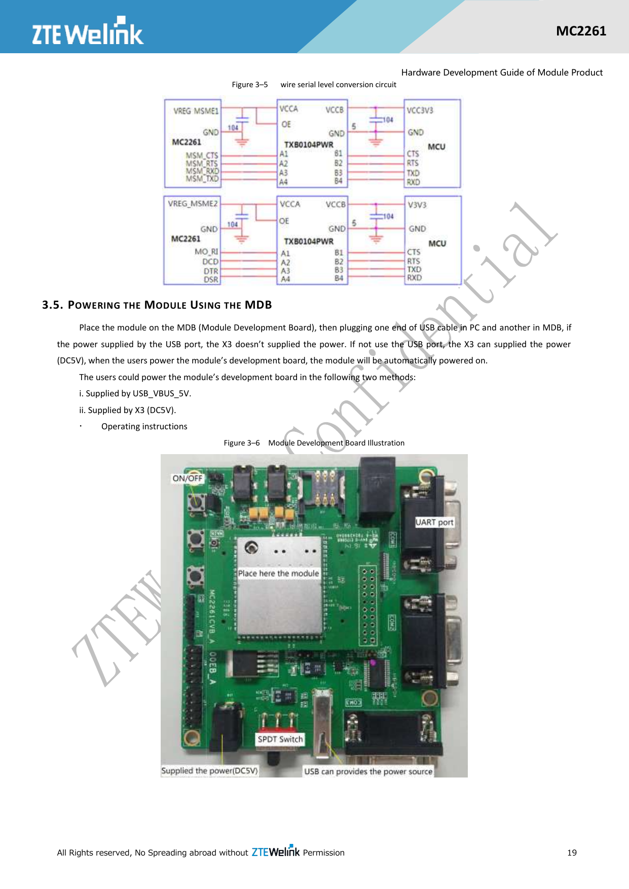
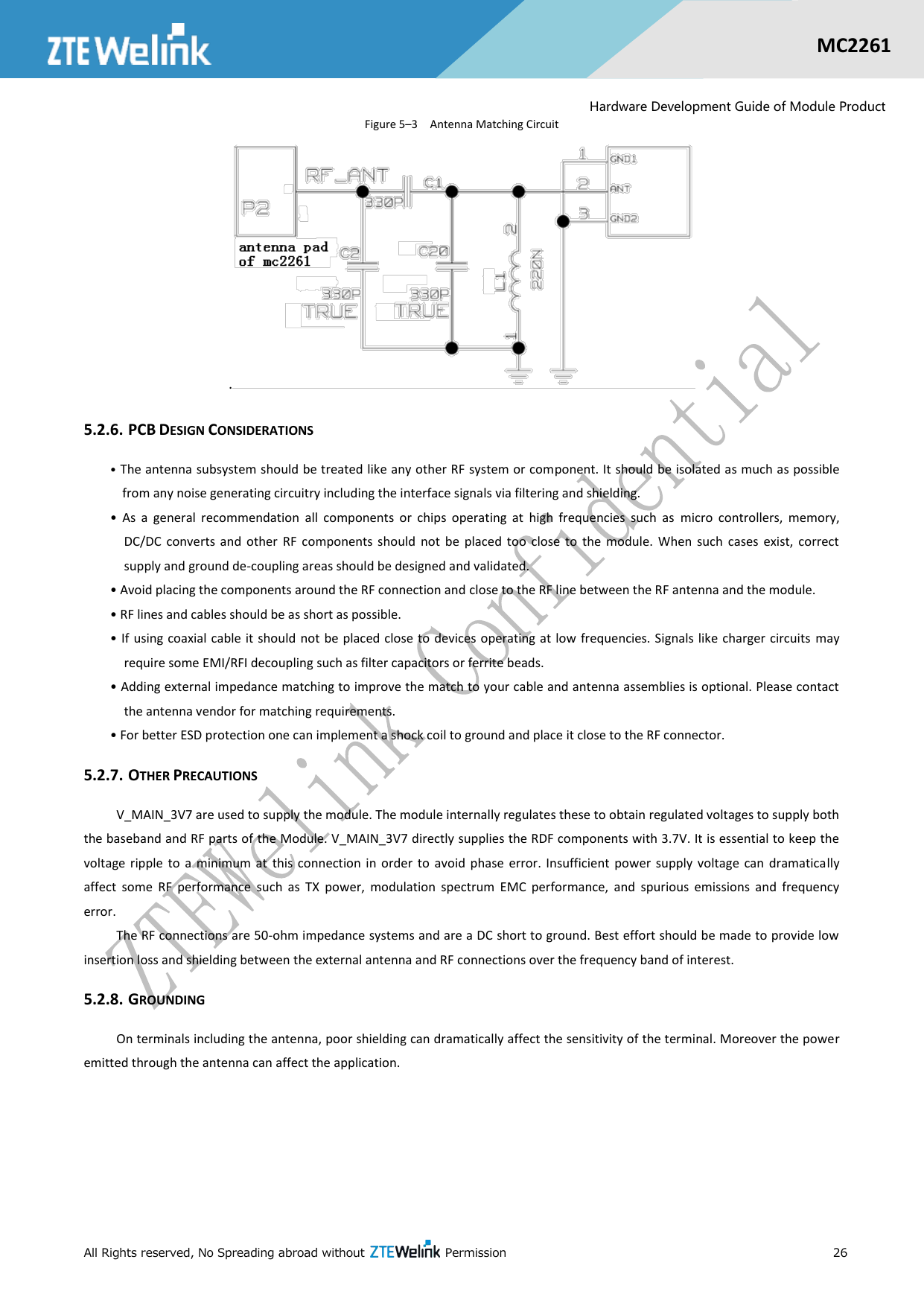
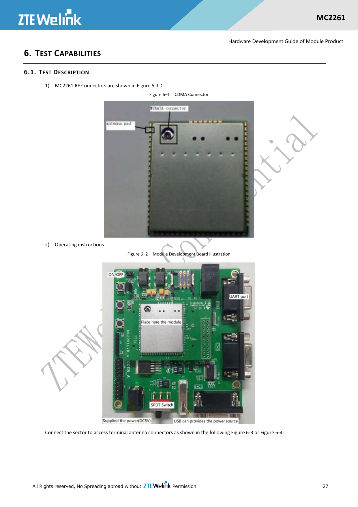
![All Rights reserved, No Spreading abroad without Permission 18 MC2261 Hardware Development Guide of Module Product Figure 3–2 USB Typical Circuit 3.4. UART Pins of MSM_CTS, MSM_RTS, MSM_RXD and MSM_TXD are 1.8V level respectively for the external interface, when connecting with level circuit which is not 1.8V will need the level switch connection. Pins of MO_RI, DCD, DTR and DSR are the level of 2.85V respectively for the external interface, when connecting with level circuit which is not 2.85V will need the level switch connection. Otherwise, UART will be unstable or module will be damaged because of the unmatched level. Figure 3-3, 3-4 and 3-5 are the references: NOTES: 1)UART must be led out[only requires the connection with RXD or TXD] for upgrading when use the module to do whole device design, USB for software upgrading is the first choice. 2)IO level is 1.8V or 2.85V. Level switch connection must be needed when 1.8V level is connected with the logic circuit which is not 1.8V[such as MCU, RS232 or driver IC MAX3238], or when 2.85V level is connected with the logic circuit which is not 2.85V[for example, RS232 or driver IC MAX3238]. Otherwise, level will be unstable or module will be damaged because of the unmatched level 3)Only RXD and TXD are needed to be connected under the condition of no flow control. RXD, TXD, /CTS and /RTS are needed to be used when selecting hardware flow control to connect other processors. All IO signal should be connected when the module is used as Modem to connect with PC. 4)Module won’t be hibernated if RxD is high level. Figure 3–3 Wire serial level conversion circuit Figure 3–4 wire serial level conversion circuit](https://usermanual.wiki/ZTE/ZTEMC2261/User-Guide-3058717-Page-19.png)