Users Manual

HARDWARE DEVELOPMENT GUIDE OF
MODULE PRODUCT
Version: V2.1
Date: 2016-04-18
CDMA Module Series
MC2261_V2
Website: www.ztewelink.com
E-mail: ztewelink@zte.com.cn
All Rights reserved, No Spreading abroad without Permission I
Hardware Development Guide of Module Product
MC2261
LEGAL INFORMATION
By receiving the document from Shenzhen ZTEWelink Technology Co., Ltd (shortly referred to as ZTEWelink), you are deemed
to have agreed to the following terms. If you don’t agree to the following terms, please stop using the document.
Copyright © 2015 Shenzhen ZTEWelink Technology Co., Ltd. All rights reserved. The document contains ZTEWelink’s
proprietary information. Without the prior written permission of ZTEWelink, no entity or individual is allowed to reproduce, transfer,
distribute, use and disclose this document or any image, table, data or other information contained in this document.
is the registered trademark of ZTEWelink. The name and logo of ZTEWelink are ZTEWelink’s trademark or
registered trademark. Meanwhile, ZTEWelink is granted to use ZTE Corporation’s registered trademark. The other products or
company names mentioned in this document are the trademark or registered trademark of their respective owner. Without the prior
written permission of ZTEWelink or the third-party oblige, no one is allowed to read this document.
The product meets the design requirements of environmental protection and personal security. The storage, use or disposal of
products should abide by the product manual, relevant contract or the laws and regulations of relevant country.
ZTEWelink reserves the right to make modifications on the product described in this document without prior notice, and keeps
the right to revise or retrieve the document any time.
If you have any question about the manual, please consult the company or its distributors promptly.
Copyright © ZTEWeLink Technology Co., LTD, All rights reserved.
All Rights reserved, No Spreading abroad without Permission II
Hardware Development Guide of Module Product
MC2261
REVISION HISTORY
Version
Date
Description
V1.0
2010-11-30
First published
V1.1
2010-12-20
Modify Table 2-1
V1.2
2011-02-22
Update image
V1.3
2011-02-25
Change Operational Temperature Range
V1.4
2011-03-07
Modify Table 2-1 and power management
V1.5
2011-03-29
Modify content of 3.1 power management and 5.2.5 antenna matching
V1.6
2011-04-25
Modify 2.1 (add note), 3.5(add new content)
V1.7
2011-06-15
Modify the email for supports.
V1.8
2011-11-25
Define pin 57 MO_RI
V1.9
2014-09-25
Update the format and template of module
Add the name of all the Figures and Tables
Update the picture of the module
Update the Figure 4-1 of NMM22-5017 connector
Update chapter 3.1 of power
Update the pins of 35&36
V2.0
2014-09-28
Update chapter 3.1 of power
Update the pins of 35
V2.1
2016-04-18
Add PID information in chapter 1.1
All Rights reserved, No Spreading abroad without Permission III
Hardware Development Guide of Module Product
MC2261
ABOUT THIS DOCUMENT
A. Application Range
R&D personnel using CDMA modules to make the second development
B. Reading Note
The symbols below are the reading notes you should pay attention on:
: Warning or Attention
: Note or Remark
CONTACT INFORMATION
Post
9/F, Tower A, Hans Innovation Mansion,
North Ring Rd., No.9018, Hi-Tech Industrial Park,
Nanshan District, Shenzhen.
Web
www.ztewelink.com
Phone
+86-755-26902600
E-Mail
ztewelink@zte.com.cn
Note: Consult our website for up-to-date product descriptions, documentation, application notes, firmware upgrades, troubleshooting tips,
and press releases
Besides, ZTEWelink provides various technical support ways to the customers, such as support by phone, website, instant
messaging, E-mail and on-site.
All Rights reserved, No Spreading abroad without Permission IV
Hardware Development Guide of Module Product
MC2261
SAFETY INFORMATION
The following safety precautions must be observed during all phases of the operation, such as usage, service or repair of any
cellular terminal or mobile incorporating ME3610 module. Manufacturers of the cellular terminal should send the following safety
information to users and operating personnel and to incorporate these guidelines into all manuals supplied with the product. If not
so, ZTEWelink does not take on any liability for customer failure to comply with these precautions.
Full attention must be given to driving at all times in order to reduce the risk of an accident. Using a
mobile while driving (even with a hands free kit) cause distraction and can lead to an accident. You must
comply with laws and regulations restricting the use of wireless devices while driving.
Switch off the cellular terminal or mobile before boarding an aircraft. Make sure it switched off. The
operation of wireless appliances in an aircraft is forbidden to prevent interference with communication
systems. Consult the airline staff about the use of wireless devices on boarding the aircraft, if your device
offers a Airplane Mode which must be enabled prior to boarding an aircraft.
Switch off your wireless device when in hospitals or clinics or other health care facilities. These
requests are designed to prevent possible interference with sensitive medical equipment.
GSM cellular terminals or mobiles operate over radio frequency signal and cellular network and
cannot be guaranteed to connect in all conditions, for example no mobile fee or an invalid SIM card. While
you are in this condition and need emergent help, please remember using emergency call. In order to make
or receive call, the cellular terminal or mobile must be switched on and in a service area with adequate
cellular signal strength.
Your cellular terminal or mobile contains a transmitter and receiver. When it is on, it receives and
transmits radio frequency energy. RF interference can occur if it is used close to TV set, radio, computer or
other electric equipment.
In locations with potentially explosive atmospheres, obey all posted signs to turn off wireless devices
such as your phone or other cellular terminals. Areas with potentially explosive atmospheres including
fuelling areas, below decks on boats, fuel or chemical transfer or storage facilities, areas where the air
contains chemicals or particles such as grain, dust or metal powders.

All Rights reserved, No Spreading abroad without Permission V
Hardware Development Guide of Module Product
MC2261
Federal Communication Commission Interference Statement
This device complies with Part 15 of the FCC Rules. Operation is subject to the following two conditions: (1) This device may not
cause harmful interference, and (2) this device must accept any interference received, including interference that may cause
undesired operation.
This equipment has been tested and found to comply with the limits for a Class B digital device, pursuant to Part 15 of the FCC Rules.
These limits are designed to provide reasonable protection against harmful interference in a residential installation. This equipment
generates, uses and can radiate radio frequency energy and, if not installed and used in accordance with the instructions, may cause
harmful interference to radio communications. However, there is no guarantee that interference will not occur in a particular
installation. If this equipment does cause harmful interference to radio or television reception, which can be determined by turning
the equipment off and on, the user is encouraged to try to correct the interference by one of the following measures:
Reorient or relocate the receiving antenna.
Increase the separation between the equipment and receiver.
Connect the equipment into an outlet on a circuit different from that
to which the receiver is connected.
Consult the dealer or an experienced radio/TV technician for help.
FCC Caution:
Any changes or modifications not expressly approved by the party responsible for compliance could void the user's authority to
operate this equipment.
This transmitter must not be co-located or operating in conjunction with any other antenna or transmitter.
Radiation Exposure Statement:
This equipment complies with FCC radiation exposure limits set forth for an uncontrolled environment. This equipment should be
installed and operated with minimum distance 20cm between the radiator & your body.
This device is intended only for OEM integrators under the following conditions:
1) The antenna must be installed such that 20 cm is maintained between the antenna and
users, and the maximum antenna gain allowed for use with this device is 4.8 dBi.
2) The transmitter module may not be co-located with any other transmitter or antenna.
As long as 2 conditions above are met, further transmitter test will not be required. However, the OEM integrator is still responsible
for testing their end-product for any additional compliance requirements required with this module installed
IMPORTANT NOTE: In the event that these conditions can not be met (for example certain laptop configurations or co-location with
another transmitter), then the FCC authorization is no longer considered valid and the FCC ID can not be used on the final product. In
these circumstances, the OEM integrator will be responsible for re-evaluating the end product (including the transmitter) and
obtaining a separate FCC authorization.
End Product Labeling
This transmitter module is authorized only for use in device where the antenna may be installed such that 20 cm may be maintained
between the antenna and users. The final end product must be labeled in a visible area with the following: “Contains FCC ID:
Q78-ZTEMC2261”. The grantee's FCC ID can be used only when all FCC compliance requirements are met.

All Rights reserved, No Spreading abroad without Permission VI
Hardware Development Guide of Module Product
MC2261
Manual Information To the End User
The OEM integrator has to be aware not to provide information to the end user regarding how to install or remove this RF module in
the user’s manual of the end product which integrates this module. The end user manual shall include all required regulatory
information/warning as show in this manual.

All Rights reserved, No Spreading abroad without Permission VII
Hardware Development Guide of Module Product
MC2261
CONTENTS
1. Mechanical Interface ............................................................................................................................................... 11
1.1. Physical Features ........................................................................................................................................................................ 11
1.2. Mechanical size .......................................................................................................................................................................... 11
2. Electrical Interface ................................................................................................................................................... 14
2.1. Pin Assignments ......................................................................................................................................................................... 14
2.2. Digital logic characteristics ......................................................................................................................................................... 16
3. Applications 17
3.1. Power Management ................................................................................................................................................................... 17
3.2. GPIO ................................................................................................................................................................................. 17
3.3. USB ................................................................................................................................................................................. 17
3.4. UART ................................................................................................................................................................................. 18
3.5. Powering the Module Using the MDB ........................................................................................................................................ 19
4. Antenna Interface .................................................................................................................................................... 21
4.1. Antenna Installation ................................................................................................................................................................... 21
4.2. Antenna Pad ............................................................................................................................................................................... 21
4.3. Antenna connector ..................................................................................................................................................................... 22
5. RF Interface ........................................................................................................................................................ 24
5.1. Overview ................................................................................................................................................................................. 24
5.2. Antenna Subsystem .................................................................................................................................................................... 25
5.2.1. Antenna Specifications .................................................................................................................................................... 25
5.2.2. Cable Loss ........................................................................................................................................................................ 25
5.2.3. Antenna Gain Minimum Requirements ........................................................................................................................... 25
5.2.4. Antenna Gain Maximum Requirements........................................................................................................................... 25
5.2.5. Antenna Matching ........................................................................................................................................................... 25
5.2.6. PCB Design Considerations .............................................................................................................................................. 26
5.2.7. Other Precautions ............................................................................................................................................................ 26
5.2.8. Grounding ........................................................................................................................................................................ 26
6. Test Capabilities ....................................................................................................................................................... 27
6.1. Test Description ......................................................................................................................................................................... 27
6.2. CDMA Test Equipment and Tools ............................................................................................................................................... 29
6.3. RF Performance Requirements .................................................................................................................................................. 30
6.3.1. CDMA2000 1X RF Rx Specification ................................................................................................................................... 30
6.3.2. CDMA2000 1X RF Tx Specification: .................................................................................................................................. 30
6.4. Environmental Reliability Requirement ..................................................................................................................................... 31
6.4.1. High Temperature Operation Test ................................................................................................................................... 31
6.4.2. Low Temperature Operation Test .................................................................................................................................... 31
6.4.3. High Temperature Storage Test ....................................................................................................................................... 32

All Rights reserved, No Spreading abroad without Permission VIII
Hardware Development Guide of Module Product
MC2261
6.4.4. Low Temperature Storage Test ........................................................................................................................................ 32
6.4.5. High Temperature High Humidity Operation Test ........................................................................................................... 32
6.4.6. Temperature Concussion Test ......................................................................................................................................... 32
6.5. Electro Magnetic Compatibility .................................................................................................................................................. 33
6.5.1. ESD Immunity Test ........................................................................................................................................................... 33
6.5.2. Radiated Emissions Test ................................................................................................................................................... 33

All Rights reserved, No Spreading abroad without Permission IX
Hardware Development Guide of Module Product
MC2261
TABLES
Table 1–1 Major Technical Parameters ................................................................................................................................................ 11
Table 2–1 MC2261 Module 68-pin Electrical Interface ........................................................................................................................ 14
Table 2–2 Baseband digital I/O characteristics for VDD_PX = 1.8 V nominal ....................................................................................... 16
Table 2–3 Baseband digital I/O characteristics for VDD_PX = 2.85 V nominal ..................................................................................... 16
Table 3–1 Input Power Characteristics ................................................................................................................................................. 17
Table 4–1 Return Loss in the Active Band ............................................................................................................................................. 21
Table 4–2 Product specifications of NMM22-5017 connector ............................................................................................................. 22
Table 4–3 Product specifications of SSMB-50TKE-10 connector .......................................................................................................... 23
Table 5–1 The requirement of dual band antenna ............................................................................................................................... 25
Table 6–1 CDMA2000 1X RF Rx Specification ....................................................................................................................................... 30
Table 6–2 CDMA2000 1X RF Tx Specification ....................................................................................................................................... 30
Table 6–3 High Temperature Operation Test ....................................................................................................................................... 31
Table 6–4 Low Temperature Operation Test ........................................................................................................................................ 31
Table 6–5 High Temperature Storage Test ........................................................................................................................................... 32
Table 6–6 Low Temperature Storage Test ............................................................................................................................................ 32
Table 6–7 High Temperature High Humidity Operation Test ............................................................................................................... 32
Table 6–8 Temperature Concussion Test ............................................................................................................................................. 32
Table 6–9 ESD Immunity Test ............................................................................................................................................................... 33
Table 6–10 Radiated Emissions Test ..................................................................................................................................................... 33

All Rights reserved, No Spreading abroad without Permission X
Hardware Development Guide of Module Product
MC2261
FIGURES
Figure 1–1 MC2261 TOP SIDE ............................................................................................................................................................... 12
Figure 1–2: MC2261 BOTTOM SIDE ......................................................................................................................................................... 12
Figure 1–3 MC2261 Module Illustration ............................................................................................................................................... 13
Figure 3–1 Powered by VBAT and VPH_PWR pin ................................................................................................................................. 17
Figure 3–2 USB Typical Circuit .............................................................................................................................................................. 18
Figure 3–3 Wire serial level conversion circuit ..................................................................................................................................... 18
Figure 3–4 wire serial level conversion circuit ...................................................................................................................................... 18
Figure 3–5 wire serial level conversion circuit .................................................................................................................................... 19
Figure 3–6 Module Development Board Illustration ............................................................................................................................ 19
Figure 3–7 First method to connect the module to RF test equipment ............................................................................................... 20
Figure 3–8 Second method to connect the module to RF test equipment ........................................................................................... 20
Figure 4–1 Specification of NMM22-5017 connector ........................................................................................................................... 22
Figure 4–2 Specification of SSMB-50TKE-10 ......................................................................................................................................... 23
Figure 5–1 CDMA Connector ................................................................................................................................................................ 24
Figure 5–2 CDMA Connector on daughter board ................................................................................................................................. 24
Figure 5–3 Antenna Matching Circuit ................................................................................................................................................... 26
Figure 6–1 CDMA Connector ................................................................................................................................................................ 27
Figure 6–2 Module Development Board Illustration ............................................................................................................................ 27
Figure 6–3 First method to connect the module to RF test equipment ............................................................................................... 28
Figure 6–4 Second method to connect the module to RF test equipment ........................................................................................... 28
Figure 6–5 First method to connect the module to RF antenna ........................................................................................................... 29
Figure 6–6 Second method to connect the module to RF antenna ...................................................................................................... 29
All Rights reserved, No Spreading abroad without Permission 11
MC2261
Hardware Development Guide of Module Product
1. MECHANICAL INTERFACE
1.1. PHYSICAL FEATURES
Table 1–1 Major Technical Parameters
Item
Specifications
Dimensions & Weight
Length: 34.4 mm
Width: 30 mm
Thickness: 3.3 mm
Weight: 8 g
Operational Temperature Range
-30℃ to +75℃
Storage Temperature Range
-40℃ to +80℃
ROHS
Yes
Antenna Connectors
50-Ohm ANT connectors for CDMA
Power Supply
Powered by the VPH_PWR pin (+3.3V~ +4.2V, typical value:3.8V)
Current
Idle current: 5mA @-75dBm, Powered by the VPH_PWR
call current: 156mA @-75dBm, Powered by the VPH_PWR
max current: 535mA @-104dBm, Powered by the VPH_PWR
CELL BAND
PID V1CP: 800M/1.9G
PID V2CP: 800M/1.9G
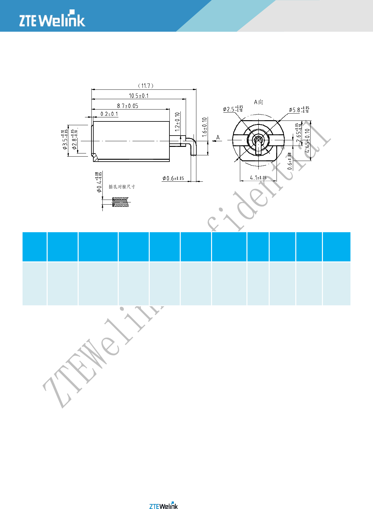
1.2. MECHANICAL SIZE
NOTE:
1. All dimensions shown in the drawing below are in the unit of mm.
2. Default dimension’s tolerance is +/-0.1mm.
All Rights reserved, No Spreading abroad without Permission 12
MC2261
Hardware Development Guide of Module Product
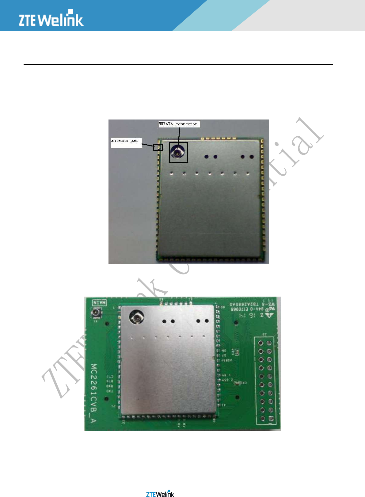
Figure 1–1 MC2261 TOP SIDE
Figure 1–2: MC2261 BOTTOM SIDE
All Rights reserved, No Spreading abroad without Permission 13
MC2261
Hardware Development Guide of Module Product
Figure 1–3 MC2261 Module Illustration
NOTE: The picture above is just for reference, please take the actual product as the referece.
All Rights reserved, No Spreading abroad without Permission 14
MC2261
Hardware Development Guide of Module Product
2. ELECTRICAL INTERFACE
2.1. PIN ASSIGNMENTS
Table 2–1 MC2261 Module 68-pin Electrical Interface
No.
Signal
Name
Signal Type
Input/output
Description
Typical
Value
Default (Internal
PU/PD)
Comments
1
GND_RF
Ground
2
RF_ANT
Analog
I/O
Connect 50ohm
antenna or feed
Connect 50ohm
antenna or feed
3
GND_RF
Ground
4
GPIO0
Digital
I/O
GPIO
1.8V
0(Output PD)
1.8V Level,
5
GPIO1
Digital
I/O
GPIO
1.8V
0(Output PD)
1.8V Level
6
GPIO2
Digital
I/O
GPIO
1.8V
0(Output PD)
1.8V Level
7
GPIO3
Digital
I/O
GPIO
1.8V
0(Output PD)
1.8V Level
8
GPIO4
Digital
I/O
GPIO
1.8V
0(Output PD)
1.8V Level
9
GPIO9
Digital
I/O
GPIO
1.8V
1.8V(Input PU)
1.8V Level
10
GPIO8
Digital
I/O
GPIO
1.8V
1.8V(Input PU)
1.8V Level
11
GPIO7
Digital
I/O
GPIO
1.8V
1.8V(Input PU)
1.8V Level
12
GPIO6
Digital
I/O
GPIO
1.8V
1.8V(Input PU)
1.8V Level
13
GPIO5
Digital
I/O
GPIO
1.8V
1.8V(Input PU)
1.8V Level
14
GND
Ground
15
MSM_CTS
I
Clear to send
UART Port
1.8V Level
16
MSM_RTS
O
Ready to send
UART Port
1.8V Level
17
MSM_RXD
I
Transmitting
data
UART Port
1.8V Level
18
MSM_TXD
O
Receiving data
UART Port
1.8V Level
19
GND
Ground
20
NA
Reserved
21
NA
Reserved
22
NA
Reserved
23
NA
Reserved
24
GND
Ground
25
NA
Reserved
26
NA
Reserved
27
GND
Ground
28
NA
Reserved
29
NA
Reserved
All Rights reserved, No Spreading abroad without Permission 15
MC2261
Hardware Development Guide of Module Product
30
NA
Reserved
31
NA
Reserved
32
GND
Ground
33
VPH_PWR
P (input)
Main power
3.8
Power range:
3.3V-4.2V
34
VPH_PWR
P (input)
Main power
3.8
Power range:
3.3V-4.2V
35
NC
Not connected
36
VBAT
P (input)
Used for
module’s power
supply
3.8
Power range:
3.3V-4.2V
37
NA
Reserved
38
GND
Ground
39
NA
Reserved
40
NA
Reserved
41
ON
Power button
Power button
42
NA
Reserved
43
NA
Reserved
44
NA
Reserved
45
NA
Reserved
46
VREG_MS
ME2
O
Digital power
2.85V
47
VREG_MS
ME1
O
Digital power
1.8V
48
NA
Reserved
49
GND
Ground
50
USB_VBUS
I
USB power
5V
51
USB_DP
Digital
B
Send D+ to USB
USB_D+ signal
52
USB_DM
Digital
B
Send D- to USB
USB_D- signal
53
GND
Ground
54
NA
Reserved
55
NA
Reserved
56
NA
Reserved
57
MO_RI
Digital
O
MSG arrival
indication
Output PU
2.85V,normal
300ms high-level
impulse when MSG
arrival
58
DCD
O
Carrier detect
2.85V
2.85V, low active
59
DTR
O
Data Terminal
2.85V
UART Port,
All Rights reserved, No Spreading abroad without Permission 16
MC2261
Hardware Development Guide of Module Product
Ready
Connect to DCD,
2.85V Level
60
DSR
I
Data Set Ready
2.85V
UART Port,
Connect to DTR, 2.85V
Level
61
NA
Reserved
62
GND
Ground
63
USE_LED
O
In-use LED
LED ON as the level is
high. 2.85V Level
64
NA
Reserved
65
NA
Reserved
66
GPIO42
Digital
I/O
GPIO
1.8V
0(Iutput PD)
1.8V Level
67
GPIO43
Digital
I/O
GPIO
1.8V
0(Iutput PD)
1.8V Level
68
GND
Ground
NOTE:
1 All the pin can be left open ,when they are not used.
2 I/O stands for Inupt/Output, P stands for Power, B stands for Bi-Directional.
3 PU/PD stands for Pull-up/Pull-down.
4 The unit of Min, Typ, Max is V.
2.2. DIGITAL LOGIC CHARACTERISTICS
Specifications for the digital I/Os of the baseband functions depend upon the pad voltage being used. The MC2261 I/O uses
two pad voltages: 1.8 and 2.85 V. Digital I/O specifications under both pad voltage conditions are presented in Table 2-2 and Table
2-3
Table 2–2 Baseband digital I/O characteristics for VDD_PX = 1.8 V nominal
Parameter
Min
Typ
Max
Unit
VIH
High-level input voltage
0.65·VDD_PX
-
VDD_PX+0.3
V
VIL
Low-level input voltage
-0.3
-
0.35·VDD_PX
V
VOH
High-level output voltage4
VDD_PX-0.45
-
VDD_PX
V
VOL
Low-level output voltage 4
0
-
0.45
V
Table 2–3 Baseband digital I/O characteristics for VDD_PX = 2.85 V nominal
Parameter
Min
Typ
Max
Unit
VIH
High-level input voltage
0.65·VDD_PX
-
VDD_PX+0.3
V
VIL
Low-level input voltage
-0.3
-
0.35·VDD_PX
V
VOH
High-level output voltage4
VDD_PX-0.45
-
VDD_PX
V
VOL
Low-level output voltage 4
0
-
0.45
V
All Rights reserved, No Spreading abroad without Permission 17
MC2261
Hardware Development Guide of Module Product
3. APPLICATIONS
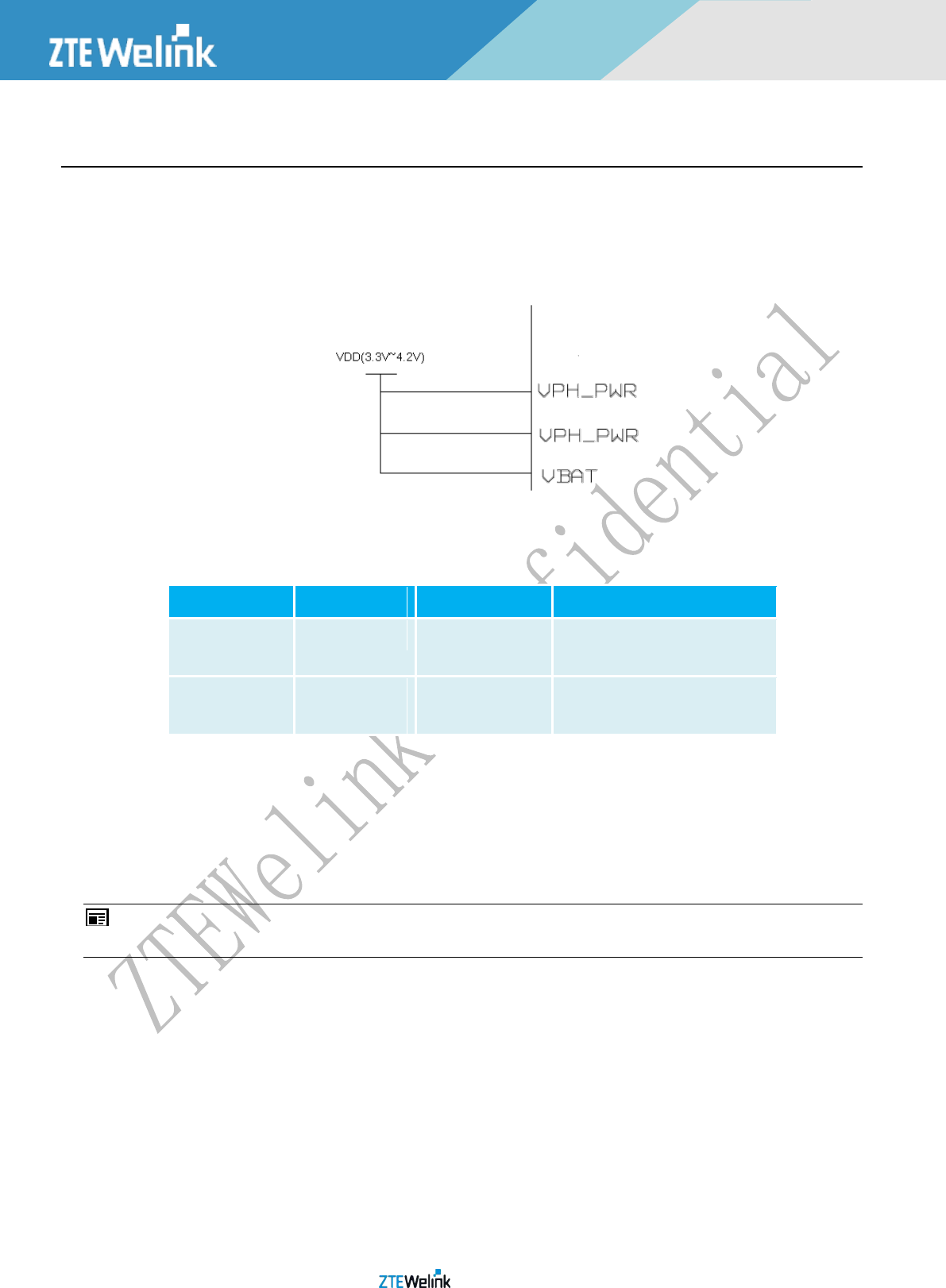
3.1. POWER MANAGEMENT
The module could work under the conditions as follows:
Connect VPH_PWR and VBAT pins together, and then connect to the power as shown in Figure 3-1.
Figure 3–1 Powered by VBAT and VPH_PWR pin
Refer to Table 3-1 for the module’s input power characteristics. If the input voltage is not in the range, it must be converted to
the voltage below:
Table 3–1 Input Power Characteristics
Status
Max. Value
Typical Volute
Min. Value
Power voltage
supply
+4.2V DC
+3.8V DC
+3.3V DC
Power current
supply
< 3mA (Average
value)
--
800mA (Depending on the network
signal condition)
When powered, the module will be automatically powered on.
3.2. GPIO
The Module have 12 GPIO,,The GPIO level is 1.8V, the logic-level voltage refer to the Table 2-2.
The GPIO input and output functions can be set by software. When the GPIO is set to output, the output drive current are
2~16mA. in the range of 2~16mA current value can be set by software. When the GPIO is set to input, it can be set to pull-up or
pull-down by software.
NOTE: The AT commands now do not support setting the GPIO functions. If you want AT commands to support the functions, the software
must be revised.
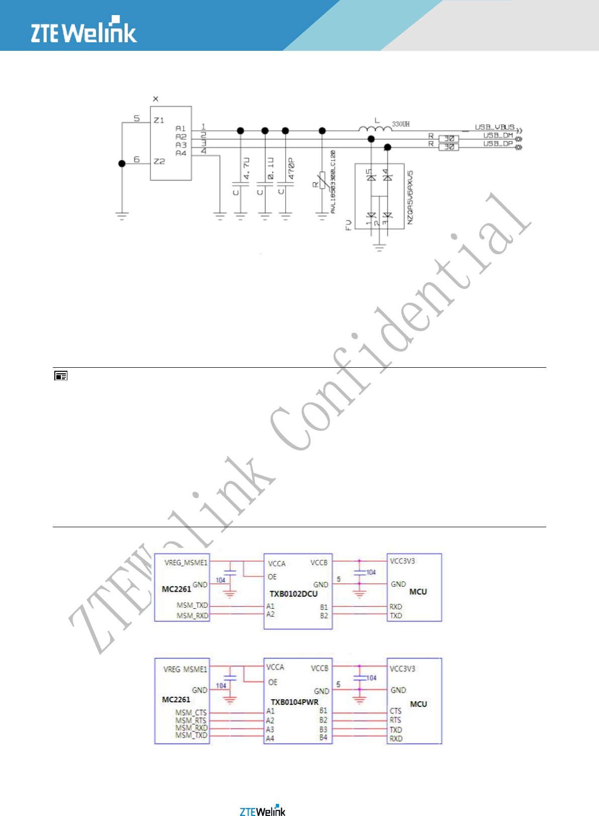
3.3. USB
The module provides a USB2.0 full-speed interface. The ESD protector and RC circuit are required to restrain EMI for USB port.
Please see Figure 3-2 for USB port.
The USB port could be used for AT command、software upgrade, RF calibration and mobile station test.
All Rights reserved, No Spreading abroad without Permission 18
MC2261
Hardware Development Guide of Module Product
Figure 3–2 USB Typical Circuit
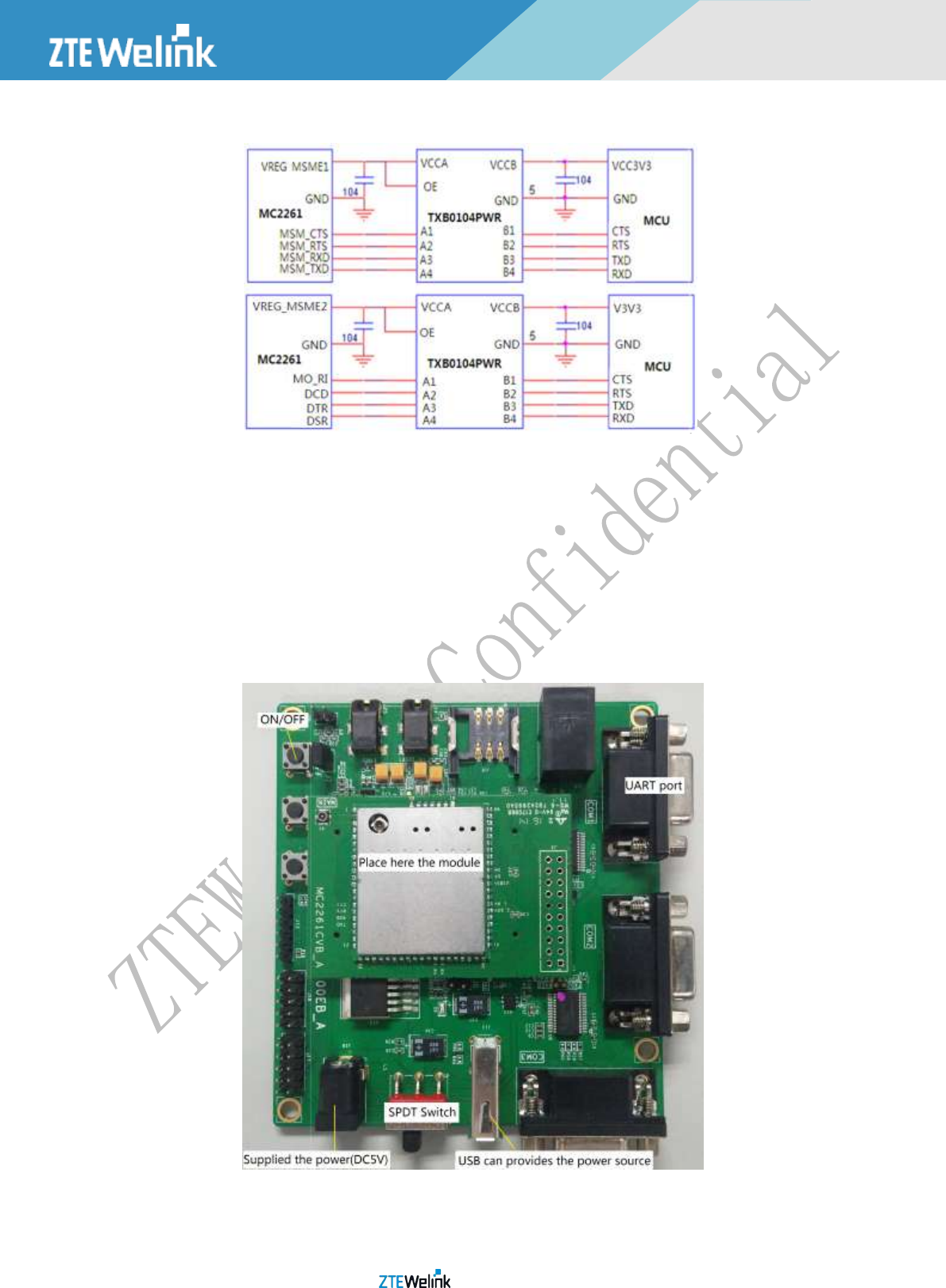
3.4. UART
Pins of MSM_CTS, MSM_RTS, MSM_RXD and MSM_TXD are 1.8V level respectively for the external interface, when connecting
with level circuit which is not 1.8V will need the level switch connection. Pins of MO_RI, DCD, DTR and DSR are the level of 2.85V
respectively for the external interface, when connecting with level circuit which is not 2.85V will need the level switch connection.
Otherwise, UART will be unstable or module will be damaged because of the unmatched level. Figure 3-3, 3-4 and 3-5 are the
references:
NOTES:
1)UART must be led out[only requires the connection with RXD or TXD] for upgrading when use the module to do whole device design, USB for
software upgrading is the first choice.
2)IO level is 1.8V or 2.85V. Level switch connection must be needed when 1.8V level is connected with the logic circuit which is not 1.8V[such as
MCU, RS232 or driver IC MAX3238], or when 2.85V level is connected with the logic circuit which is not 2.85V[for example, RS232 or driver IC
MAX3238]. Otherwise, level will be unstable or module will be damaged because of the unmatched level
3)Only RXD and TXD are needed to be connected under the condition of no flow control. RXD, TXD, /CTS and /RTS are needed to be used when
selecting hardware flow control to connect other processors. All IO signal should be connected when the module is used as Modem to connect
with PC.
4)Module won’t be hibernated if RxD is high level.
Figure 3–3 Wire serial level conversion circuit
Figure 3–4 wire serial level conversion circuit
All Rights reserved, No Spreading abroad without Permission 19
MC2261
Hardware Development Guide of Module Product
Figure 3–5 wire serial level conversion circuit
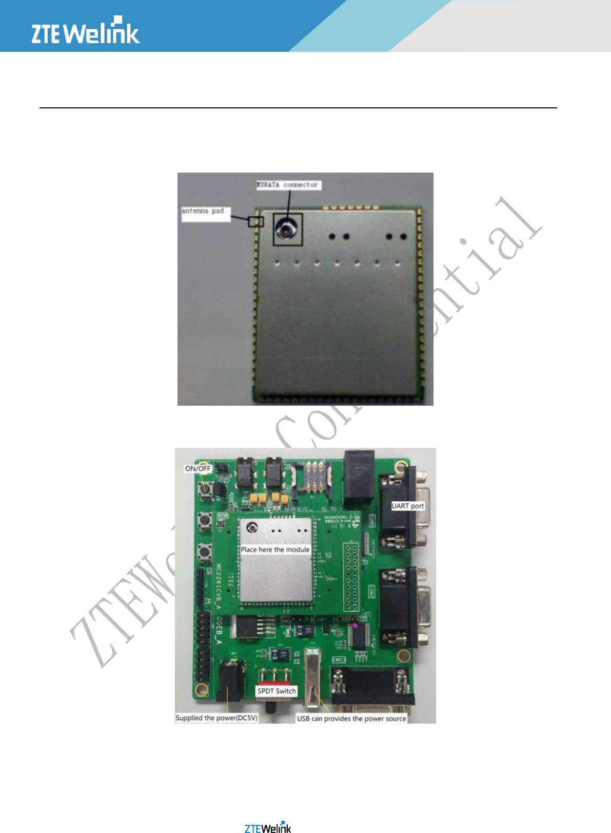
3.5. POWERING THE MODULE USING THE MDB
Place the module on the MDB (Module Development Board), then plugging one end of USB cable in PC and another in MDB, if
the power supplied by the USB port, the X3 doesn’t supplied the power. If not use the USB port, the X3 can supplied the power
(DC5V), when the users power the module’s development board, the module will be automatically powered on.
The users could power the module’s development board in the following two methods:
i. Supplied by USB_VBUS_5V.
ii. Supplied by X3 (DC5V).
Operating instructions
Figure 3–6 Module Development Board Illustration
All Rights reserved, No Spreading abroad without Permission 20
MC2261
Hardware Development Guide of Module Product
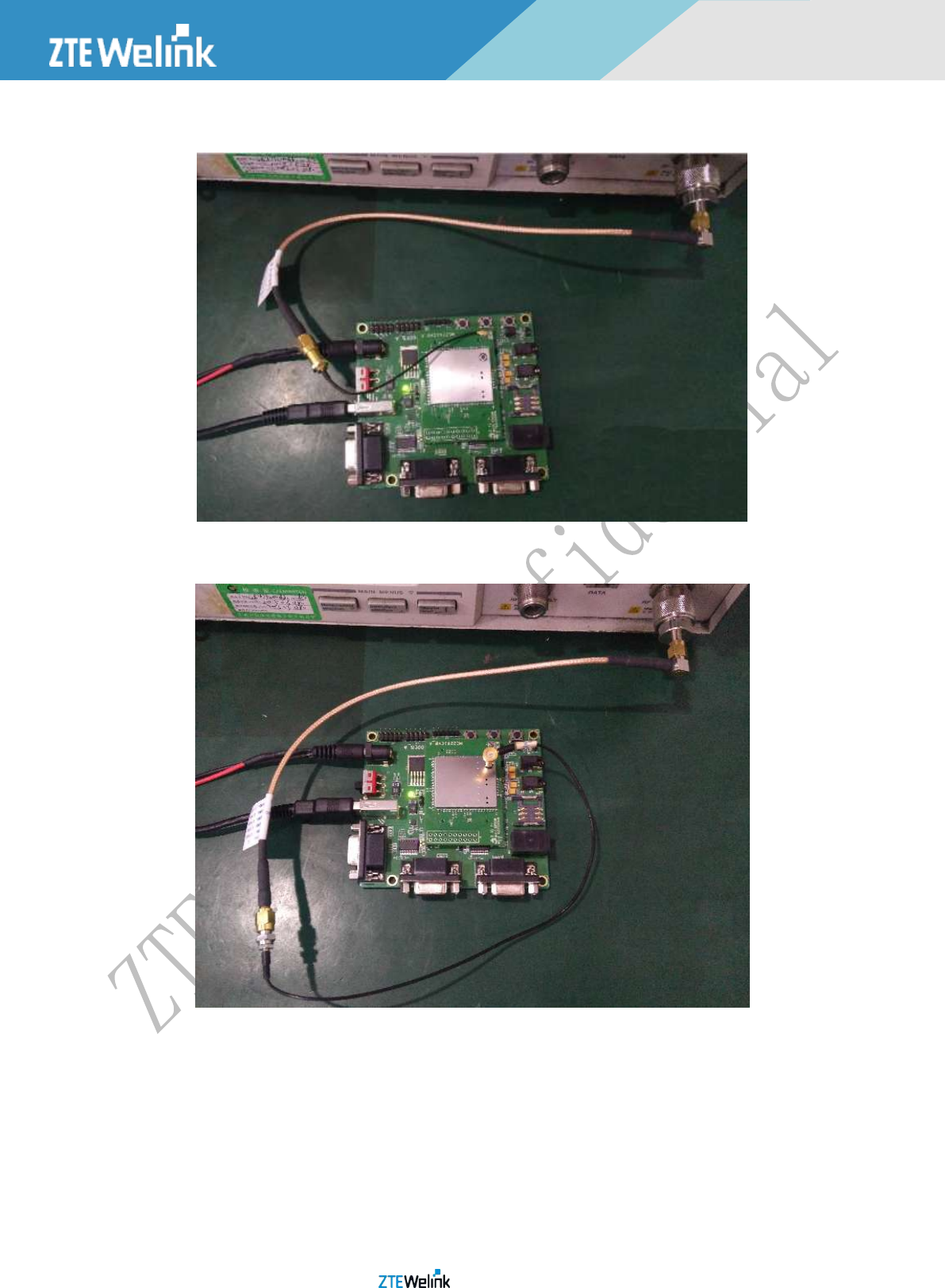
Connect the sector to access terminal antenna connectors as shown in the following Figure 3-8 or Figure 3-9.
Figure 3–7 First method to connect the module to RF test equipment
Figure 3–8 Second method to connect the module to RF test equipment
All Rights reserved, No Spreading abroad without Permission 21
MC2261
Hardware Development Guide of Module Product
4. ANTENNA INTERFACE
The RF interface of the MC2261 Module has an impedance of 50 ohm. The module is capable of sustaining a total mismatch at
the antenna connector or pad without any damage, even when transmitting at maximum RF power.
The external antenna must be matched properly to achieve best performance regarding radiated power, DC-power
consumption, modulation accuracy and harmonic suppression. Antenna matching networks are not included on the MC2261 Module
PCB and should be placed in the host application.
Regarding the return loss, the Module provides the following values in the active band:
Table 4–1 Return Loss in the Active Band
State of Module
Return Loss of Module
Recommended Return Loss of Application
Receive
≥ 8dB
≥ 12dB
Transmit
not applicable
≥ 12dB
The connection of the antenna or other equipment must be de coupled from DC voltage. This is necessary because the antenna
connector is DC coupled to ground via an inductor for ESD protection.
4.1. ANTENNA INSTALLATION
To suit the physical design of individual applications, the MC2261 offers two alternatives approached to connecting the
antenna:
■ Recommended approach: CS-G2-SS1S-1.6S antenna connector manufactured by Percsson assembled on the daughter board.
See Section 4.3 for details. CS-G2-SS1S-1.6D antenna connector manufactured by Percsson assembled on the component side
of the PCB (top view on Module). See Section 4.3 for details.
■ Antenna pad and grounding plane placed on the bottom side. See Section 4.2 for details.
The SSMB-50TKE-10 and NMM22-5017 connectors have been chosen as antenna reference point (ARP) for the ZTE reference
equipment submitted to type approve the MC2261 Module. All RF data specified throughout this manual are related to the ARP. For
compliance with the test results of the ZTE type approval you are advised to give priority to the connector, rather than using the
antenna pad.
NOTE: Both solutions can be applied alternatively. This means, if the antenna is connected to the pad, then the connector on the Module
must be left empty. If the antenna is connected to daughter board, the connector on the Module must be left empty too. And when the antenna is
connected to the Module connector, the pad is useless.
4.2. ANTENNA PAD
The antenna pad of the module is soldered to the board on the customer design to connect with RF line.
For proper grounding connect the RF line to the ground plane on the bottom of the MC2261 Module which must be connected
to the ground plane of the application.
Consider that according to CDMA recommendations as 50Ω connector is mandatory for type approval measurements. It must
be ensured that the RF line which is connected to antenna pad should be controlled on 50Ω.
Notes on soldering
■ To prevent damage to the Module and to obtain long-term solder joint properties, you are advised to maintain the standards
of good engineering practice for soldering.
All Rights reserved, No Spreading abroad without Permission 22
MC2261
Hardware Development Guide of Module Product
Material Properties
■ MC2261 Module PCB: FR4
■ Antenna pad: Gold plated pad
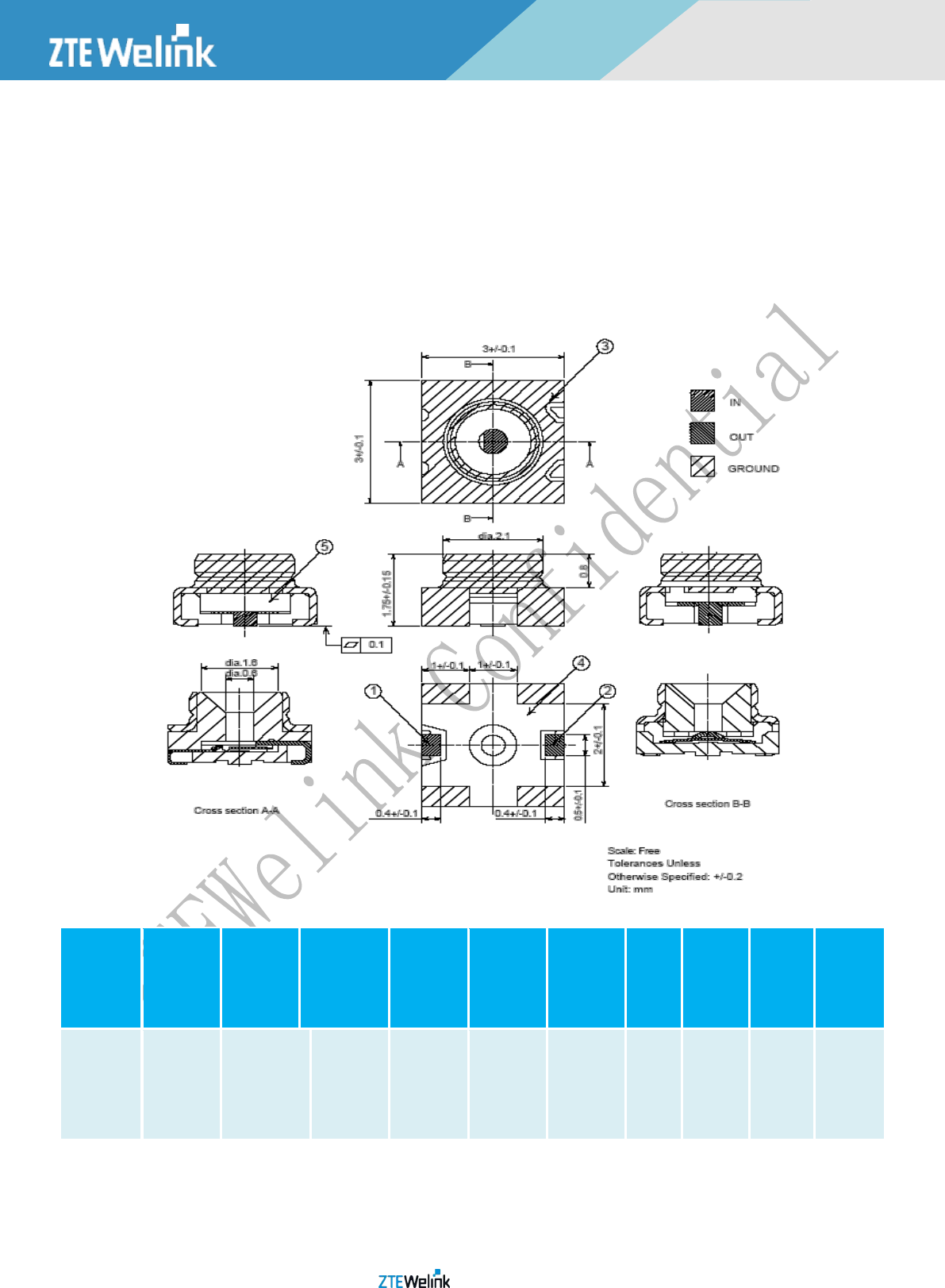
4.3. ANTENNA CONNECTOR
The MC2261 Module uses a microwave coaxial connector supplied by Murata Ltd. The product name is NMM22-5017. The
position of the antenna connector on the Module PCB can be seen in Figure 5-1.
Figure 4–1 Specification of NMM22-5017 connector
Table 4–2 Product specifications of NMM22-5017 connector
Rated
Voltage
(V)
Contact
Resistance
(ohm)
With
standing
Voltage
(rms)
Insulation
Resistance
(M ohm)
Durability
(cycles)
Frequency
Rating
(GHz)
TEMP
Range
(degree C)
VSWR
Center
Contact
Outer
Contact
Insulator
250
0.05
max.
300 (AC)
500 min.
500
DC - 6.0
-40~+90
1.2
max.
(DC~3
GHz)
Copper
Alloy
Gold
plated
Copper
Alloy
Silver
plated
Engineeri
ng plastic
Impedance: 50 ohm
All Rights reserved, No Spreading abroad without Permission 23
MC2261
Hardware Development Guide of Module Product
The daughter board of MC2261 Module uses a microwave coaxial connector supplied by CNT Ltd. The product name is
SSMB-50TKE-10. The position of the antenna connector on the daughter PCB can be seen in Figure 5-2.
Figure 4–2 Specification of SSMB-50TKE-10
Table 4–3 Product specifications of SSMB-50TKE-10 connector
Rated
Voltage
(V)
Contact
Resistance
(ohm)
Withstanding
Voltage
(rms)
Insulation
Resistance
(M ohm)
Durability
(cycles)
Frequency
Rating
(GHz)
Temperature
Range
(degree C)
VSWR
Center
Contact
Outer
Contact
Insulator
250
0.05 max.
300 (AC)
1000 min.
5000
DC - 3.0
-55~+155
1.35
max.
(DC~3
GHz)
Copper
Alloy
Gold
plated
Copper
Alloy
Silver
plated
Engineerin
g plastic
Impedance: 50 ohm
All Rights reserved, No Spreading abroad without Permission 24
MC2261
Hardware Development Guide of Module Product
5. RF INTERFACE
5.1. OVERVIEW
A 50 ohm coaxial RF connector is provided for Module testing. However, we advise customers lead from the antenna pad at
the RF line to the antenna.
Figure 5–1 CDMA Connector
Another 50 ohm coaxial RF connector on daughter board is provided for Module testing and customer showing.
Figure 5–2 CDMA Connector on daughter board
The integrator must provide a suitable antenna that works in the desired frequency band of operation. The Antenna connected
to the CDMA connector should be a dual band antenna supporting the US PCS and Cellular bands.
All Rights reserved, No Spreading abroad without Permission 25
MC2261
Hardware Development Guide of Module Product
Table 5–1 The requirement of dual band antenna
NOTE: TX refers to the transmit from the module into the antenna (Reverse Link of the CDMA system), and RX refers to the receive from the
antenna into the module (Forward Link of the CDMA system).
5.2. ANTENNA SUBSYSTEM
The antenna sub-system and its design is a major part of the final product integration. Special attention and care should be
taken in adhering to the following guidelines.
5.2.1. ANTENNA SPECIFICATIONS
Choice of the antenna cable (type, length, performance, RF loss, etc) and antenna connector (type + losses) can have a major
impact on the success of the design.
5.2.2. CABLE LOSS
All cables have RF losses. Minimizing the length of the cable between the antenna and the RF connectors on the module will
help obtain superior performance. High Quality/Low loss co-axial cables should be used to connect the antenna to the RF connectors.
Contact the antenna vendor for the specific type of cable that interfaces with their antenna and ask them to detail the RF losses of
the cables supplied along with the antenna. Typically, the cable length should be such that they have no more than 1-2dB of loss.
Though the system will work with longer (lossy) cables, this will degrade CDMA system performance. Care should also be taken to
ensure that the cable end connectors/terminations are well assembled to minimize losses and to offer a reliable, sturdy connection
to the Module sub-system. This is particularly important for applications where the module is mounted on a mobile or portable
environment where it is subject to shock and vibration.
5.2.3. ANTENNA GAIN MINIMUM REQUIREMENTS
It is recommended that the antenna chosen have at least 2 dBi gain in the cellular band and 4 dBi in the PCS band. The Antenna
subsystem shall also have at least 8 dB of return loss at the input with respect to a 50-ohm system.
5.2.4. ANTENNA GAIN MAXIMUM REQUIREMENTS
Our FCC Grant imposes a maximum gain for the antenna subsystem: 7 dBi for the Cellular band and 13dBi for the PCS band.
Warning: Excessive gain could damage sensitive RF circuits and void the warranty.
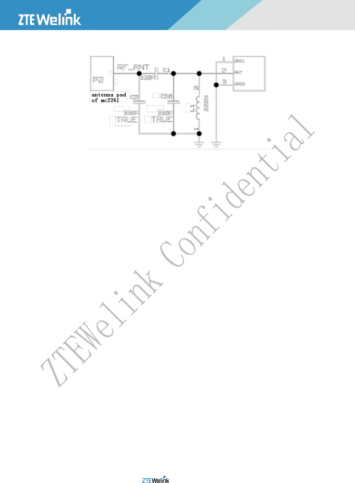
5.2.5. ANTENNA MATCHING
The module’s RF connectors are designed to work with a 50-ohm subsystem. It is assumed that the antenna chosen has
matching internal to it to match between the 50-ohm RF connectors and the antenna impedance.
Band
TX Frequency
RX Frequency
PCS
1850-1910 MHz
1930-1990 MHz
Cellular
824-849 MHz
869-894 MHz
All Rights reserved, No Spreading abroad without Permission 26
MC2261
Hardware Development Guide of Module Product
Figure 5–3 Antenna Matching Circuit
.
5.2.6. PCB DESIGN CONSIDERATIONS
• The antenna subsystem should be treated like any other RF system or component. It should be isolated as much as possible
from any noise generating circuitry including the interface signals via filtering and shielding.
• As a general recommendation all components or chips operating at high frequencies such as micro controllers, memory,
DC/DC converts and other RF components should not be placed too close to the module. When such cases exist, correct
supply and ground de-coupling areas should be designed and validated.
• Avoid placing the components around the RF connection and close to the RF line between the RF antenna and the module.
• RF lines and cables should be as short as possible.
• If using coaxial cable it should not be placed close to devices operating at low frequencies. Signals like charger circuits may
require some EMI/RFI decoupling such as filter capacitors or ferrite beads.
• Adding external impedance matching to improve the match to your cable and antenna assemblies is optional. Please contact
the antenna vendor for matching requirements.
• For better ESD protection one can implement a shock coil to ground and place it close to the RF connector.
5.2.7. OTHER PRECAUTIONS
V_MAIN_3V7 are used to supply the module. The module internally regulates these to obtain regulated voltages to supply both
the baseband and RF parts of the Module. V_MAIN_3V7 directly supplies the RDF components with 3.7V. It is essential to keep the
voltage ripple to a minimum at this connection in order to avoid phase error. Insufficient power supply voltage can dramatically
affect some RF performance such as TX power, modulation spectrum EMC performance, and spurious emissions and frequency
error.
The RF connections are 50-ohm impedance systems and are a DC short to ground. Best effort should be made to provide low
insertion loss and shielding between the external antenna and RF connections over the frequency band of interest.
5.2.8. GROUNDING
On terminals including the antenna, poor shielding can dramatically affect the sensitivity of the terminal. Moreover the power
emitted through the antenna can affect the application.
All Rights reserved, No Spreading abroad without Permission 27
MC2261
Hardware Development Guide of Module Product
6. TEST CAPABILITIES
6.1. TEST DESCRIPTION
1) MC2261 RF Connectors are shown in Figure 5-1:
Figure 6–1 CDMA Connector
2) Operating instructions
Figure 6–2 Module Development Board Illustration
Connect the sector to access terminal antenna connectors as shown in the following Figure 6-3 or Figure 6-4:
All Rights reserved, No Spreading abroad without Permission 28
MC2261
Hardware Development Guide of Module Product
Figure 6–3 First method to connect the module to RF test equipment
Figure 6–4 Second method to connect the module to RF test equipment
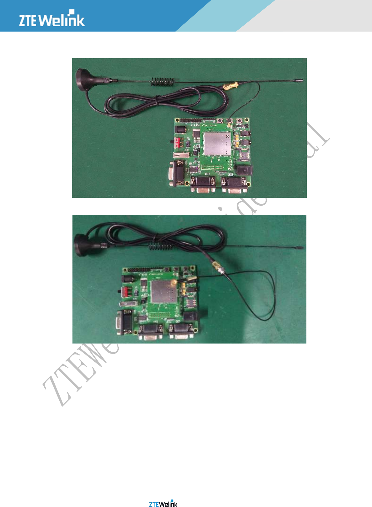
Connect the RF antenna to terminal antenna connectors as shown in the following Figure 6-5 or Figure 6-6:
All Rights reserved, No Spreading abroad without Permission 29
MC2261
Hardware Development Guide of Module Product
Figure 6–5 First method to connect the module to RF antenna
Figure 6–6 Second method to connect the module to RF antenna
6.2. CDMA TEST EQUIPMENT AND TOOLS
Lease or purchase of test equipment is available from vendors who provide this equipment for CDMA over the-air simulation.
Some suggested products include:
• Agilent 8960 Series 10 E5515C CDMA Mobile Station Tester
• Agilent E4440A Spectrum analyzer
• Agilent E4438C Signal Generator
• Agilent E4438C Signal Generator
• Programmable Temperature-Humidity Testor
• Programmable Temperature Concussion Testor
All Rights reserved, No Spreading abroad without Permission 30
MC2261
Hardware Development Guide of Module Product
6.3. RF PERFORMANCE REQUIREMENTS
6.3.1. CDMA2000 1X RF RX SPECIFICATION
Table 6–1 CDMA2000 1X RF Rx Specification
Frequency range
869~894MHz/1930~1990MHZ
Rx. Sensitivity
-104 dBm(FER≤0.5%)
Rx. Signal Range
-25 dBm~ -104dBm(FER≤0.5%)
Immunity
FER≤1.0%(-101dBm/BW , 30dBm@±900KHz) (800MHz)
FER≤1.0%(-101dBm/BW ,-40dBm@±1250KHz) (1900MHz)
Inter-modulation spurious
emissions
FER≤1.0%(Test1: -101dBm/BW ,+900/+1700KHz, -43dBm)
FER≤1.0%(Test1: -101dBm/BW ,+1250/+2050KHz, -43dBm)
FER≤1.0%(Test 2: -101dBm/BW ,-900/-1700KHz, -43dBm)
FER≤1.0%(Test 2: -101dBm/BW,-1250/-2050KHz, -43dBm)
Conductive spurious
emissions
<-76dBm/1MHz(1930~1990MHz ; 869~894MHz)
< - 61dBm/1MHz(1850~1910MHz ; 824~849MHz)
< - 47dBm/30KHz(other frequency)
Demodulation of forward
traffic channel in AWGN
FER≤3.0%(Test 1: Rate Group 1(9600bps)
FER≤1.0%(Test 2: Rate Group 1(9600bps)
FER≤0.5%(Test 3: Rate Group 1(9600bps)
FER≤1.0%(Test 4: Rate Group 1(4800bps)
FER≤1.0%(Test 5: Rate Group 1(2400bps)
FER≤1.0%(Test 6: Rate Group 1(1200bps)
FER≤3.0%(Test 7: Rate Group 2(14400bps)
FER≤1.0%(Test 8: Rate Group 2(14400bps)
FER≤0.5%(Test 9: Rate Group 2(14400bps)
FER≤1.0%(Test 10: Rate Group 2(7200bps)
FER≤1.0%(Test 11: Rate Group 2(3600bps)
FER≤1.0%(Test 12: Rate Group 2(1800bps)
6.3.2. CDMA2000 1X RF TX SPECIFICATION:
Table 6–2 CDMA2000 1X RF Tx Specification
Max. frequency tolerance
824~849MHz/1850~1910MHz
Max. Tx. Power
±300Hz/±150Hz
Min. output power
800MHz: 23dBm ~ 30dBm@-105.5 dBm
1900MHz: 18dBm ~ 27dBm@-105.5 dBm
Standby output power
< -50dBm@-25 dBm
All Rights reserved, No Spreading abroad without Permission 31
MC2261
Hardware Development Guide of Module Product
Code domain power
<-61dBm
Transmitter time error
±1.0μs
Waveform quality factor
>0.944
Open loop power control
(Test 1: -25dBm/1.23MHz)-48dBm/1.23MHz±9.5dBm
(Test 1: -25dBm/1.23MHz)-51dBm/1.23MHz±9.5dBm
(Test 2: -65dBm/1.23MHz)-8dBm/1.23MHz±9.5dBm
(Test 2: -65dBm/1.23MHz)-11dBm/1.23MHz±9.5dBm
(Test 3: -93.5dBm/1.23MHz)+20dBm/1.23MHz±9.5dBm
(Test 3: -91.3dBm/1.23MHz)+15dBm/1.23MHz±9.5dBm
Close loop power control
±24dB(9600bps data rate)
±24dB(4800bps data rate)
±24dB(2400bps data rate)
±24dB(1200bps data rate)
Conductive spurious emissions
-42dBc/30KHz or -54dBm/1.23MHz(|Δf|: 1.25MHz~1.98MHz)
-54dBc/30KHz or -54dBm/1.23MHz(|Δf|: 1.98MHz~4.00MHz)
< -13dBm/1KHz(f> 4MHz, 9KHz < f < 150KHz,)
< -13dBm/10KHz(f > 4MHz, 150KHz <f < 30MHz)
< -13dBm/100KHz(f > 4MHz, 30MHz < f < 1GHz)
< -13dBm/1MHz(f> 4MHz, 1GHz < f < 10GHz)
Remarks: RF technical specification conforms to the following standards:
3GPP2 C.S0011-C V2.0 Recommended Minimum Performance Standards for cdma2000 Spread Spectrum Mobile Stations
3GPP2 C.S0033-0 V2.0 Recommended Minimum Performance Standards for cmda2000 High Rate Packet Data Access Terminal
6.4. ENVIRONMENTAL RELIABILITY REQUIREMENT
6.4.1. HIGH TEMPERATURE OPERATION TEST
Table 6–3 High Temperature Operation Test
EUT Status
Power-on
Temperature
70℃
Duration
16h
6.4.2. LOW TEMPERATURE OPERATION TEST
Table 6–4 Low Temperature Operation Test
EUT Status
Power-on
Temperature
-25℃
Duration
16h
All Rights reserved, No Spreading abroad without Permission 32
MC2261
Hardware Development Guide of Module Product
6.4.3. HIGH TEMPERATURE STORAGE TEST
Table 6–5 High Temperature Storage Test
EUT Status
Power-off
Temperature
85℃
Duration
24h
6.4.4. LOW TEMPERATURE STORAGE TEST
Table 6–6 Low Temperature Storage Test
EUT Status
Power-off
Temperature
-45℃
Duration
24h
6.4.5. HIGH TEMPERATURE HIGH HUMIDITY OPERATION TEST
Table 6–7 High Temperature High Humidity Operation Test
EUT Status
Power-on
Temperature
55℃
Humidity
93%
Duration
48h
6.4.6. TEMPERATURE CONCUSSION TEST
Table 6–8 Temperature Concussion Test
EUT Status
Power-off
High Temperature
85℃
High Temperature Duration
1h
Low Temperature
-45℃
Low Temperature Duration
1h
Cycle Times
10
All Rights reserved, No Spreading abroad without Permission 33
MC2261
Hardware Development Guide of Module Product
6.5. ELECTRO MAGNETIC COMPATIBILITY
6.5.1. ESD IMMUNITY TEST
Table 6–9 ESD Immunity Test
EUT Status
Idle mode and traffic mode
Test Voltage
Air ±8KV; Contact ±6KV
Reference Standard
IEC 61000-4-2 : 2001
6.5.2. RADIATED EMISSIONS TEST
Table 6–10 Radiated Emissions Test
EUT Status
Idle mode and traffic mode
Limits for radiated disturbance
Class B ITE
Reference Standard
FCC Part15