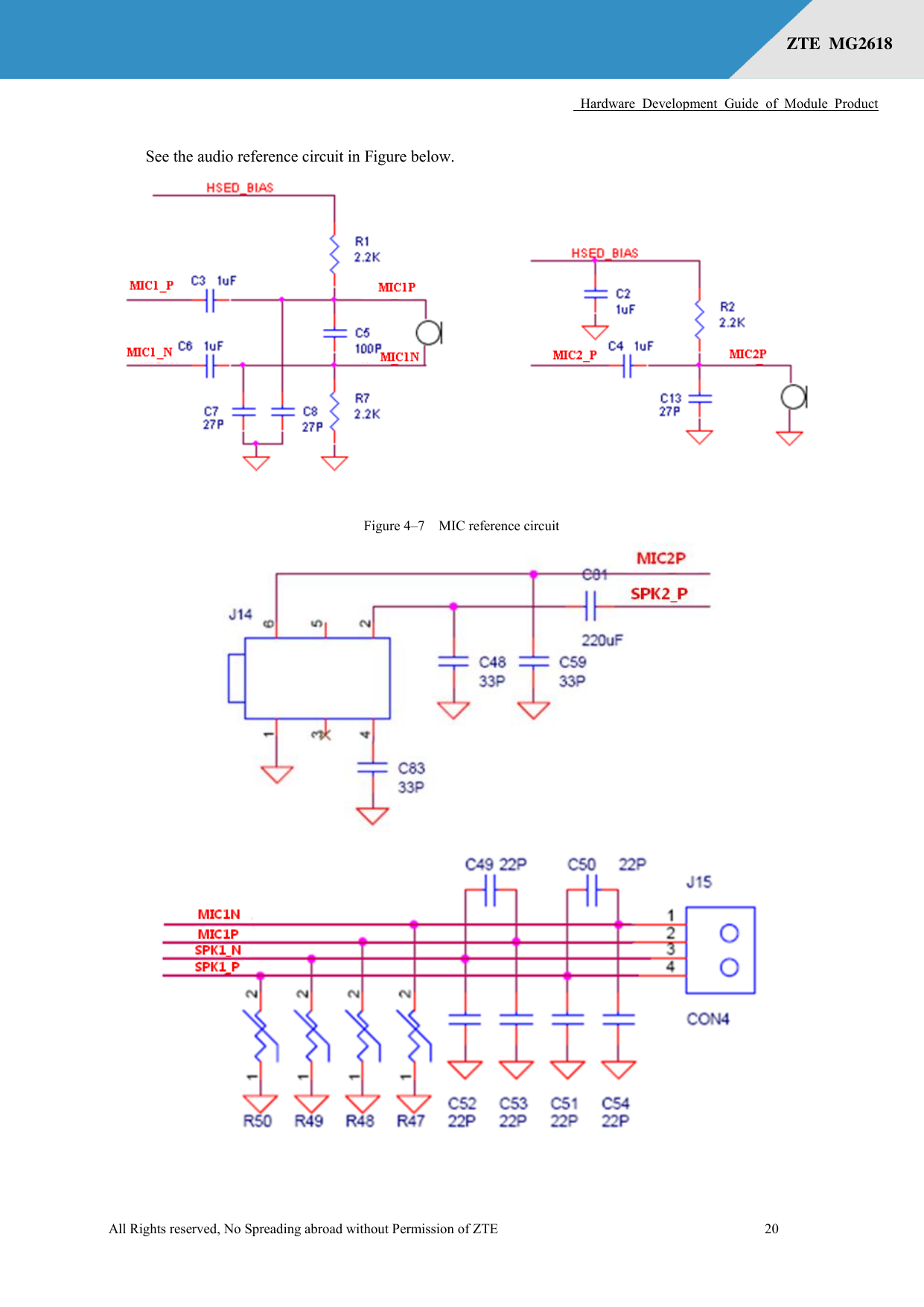
ZTE ZTEMG2618 GSM Wireless Data Terminal User Manual

ZTE Corporation GSM Wireless Data Terminal Users Manual

Users Manual

               Hardware Development Guide of Module Product  ZTE  MG2618 Version 1.0,2015-03-18 Welink Your Smart
     Hardware  Development  Guide  of  Module  Product  All Rights reserved, No Spreading abroad without Permission of ZTE              I ZTE  MG2618    Legal Information By accepting this certain document of ZTE CORPORATIN you agree to the following terms. If you do not agree to the following terms, please notice that you are not allowed to use this document.  Copyright © 2009 ZTE CORPORATION. Any rights not expressly granted herein are reserved. This document  contains  proprietary  information  of  ZTE  CORPORATION.  Any  reproduction,  transfer, distribution, use or disclosure of this document or any portion of this document, in any form by any means, without the prior written consent of ZTE CORPORATION is prohibited.   and   are registered trademarks of ZTE CORPORATION. ZTE’s company name, logo and  product  names  referenced  herein  are  either  trademarks  or  registered  trademarks  of  ZTE CORPORATION. Other product and company names mentioned herein may be  trademarks or trade names of their respective owners. Without the prior written consent of ZTE CORPORATION or the third party owner thereof, anyone’s  access  to  this  document  should  not  be  construed  as  granting,  by implication, estopped or otherwise, any license or right to use any marks appearing in the document.  The  design  of  this  product  complies  with  requirements  of  environmental  protection  and  personal security. This product shall be stored, used or discarded in accordance with product manual, relevant contract or laws and regulations in relevant country (countries).  This document is provided “as is” and “as available”. Information contained in this document is subject to continuous update without further notice due to improvement and update of ZTE CORPORATION’s products and technologies.
     Hardware  Development  Guide  of  Module  Product  All Rights reserved, No Spreading abroad without Permission of ZTE              II ZTE  MG2618   Revision History Version Date Description V1.0 2015-03-18 1st released
     Hardware  Development  Guide  of  Module  Product  All Rights reserved, No Spreading abroad without Permission of ZTE              III ZTE  MG2618   Contents  1 PRODUCT OVERVIEW ............................................................................................................. 1 1.1  TECHNICAL PARAMETERS ............................................................................................ 1 1.2  APPLICATION FRAME ..................................................................................................... 2 1.3  ABBREVIATIONS.............................................................................................................. 3 2 INTERFACES ............................................................................................................................... 6 2.1  PIN DESCRIPTION ............................................................................................................ 6 2.2  ANTENNA INTERFACE ................................................................................................... 8 2.3  RF PERFORMANCE OF ANTENNA INTERFACE ......................................................... 8 3 ELECTRIC FEATURES ........................................................................................................... 10 3.1  INTERFACE POWER LEVEL ......................................................................................... 10 3.2  POWER CONSUMPTION ................................................................................................ 10 3.3  POWER-ON/OFF TIMING SEQUENCE ......................................................................... 11 3.4  RELIABILITY TEST ........................................................................................................ 11 3.5  ESD CHARACTERISTIC ................................................................................................. 12 3.6  GPS PERFORMANCE ...................................................................................................... 12 4 REFERENCE CIRCUIT OF MODULE INTERFACES ....................................................... 13 4.1  RESET AND POWER DESIGNING ................................................................................ 13 4.2  UART INTERFACE .......................................................................................................... 15 4.2.1  DUPLEX UART INTERFACE .............................................................................. 17 4.3  SIM CARD INTERFACE .................................................................................................. 18 4.4  AUDIO INTERFACE ........................................................................................................ 19 4.5  LED INDICATOR INTERFACE ...................................................................................... 22 4.6  GPS INTERFACE ............................................................................................................. 22 4.7  CONNECTION METHOD OF GPS ACTIVE ANTENNA.............................................. 23 5 MECHANIC FEATURES.......................................................................................................... 24 5.1  APPEARANCE DIAGRAM ............................................................................................. 24 5.2  ASSEMBLY DIAGRAM .................................................................................................. 25 5.3  PCB PACKAGE DIMENSIONS ....................................................................................... 26
     Hardware  Development  Guide  of  Module  Product  All Rights reserved, No Spreading abroad without Permission of ZTE              IV ZTE  MG2618   6 SMT PROCESS AND BAKING GUIDE .................................................................................. 28 6.1  STORAGE REQUIREMENTS.......................................................................................... 28 6.2  RECOMMENDED PAD DESIGN .................................................................................... 28 6.3  REQUIREMENTS OF MODULE’S POSITION ON MAIN BOARD ............................. 30 6.4  MODULE PLANENESS STANDARD ............................................................................ 31 6.5  PROCESS ROUTING SELECTION ................................................................................. 31 6.5.1  SOLDER PASTE SELECTION.............................................................................. 31 6.5.2  DESIGN OF MODULE PAD’S STEEL MESH OPENING ON MAIN BOARD . 31 6.5.3  MODULE BOARD’S SMT PROCESS .................................................................. 32 6.5.4  MODULE SOLDERING REFLOW CURVE ........................................................ 33 6.5.5  REFLOW METHOD .............................................................................................. 34 6.5.6  MAINTENANCE OF DEFECTS ........................................................................... 34 6.6  MODULE’S BAKING REQUIREMENTS ....................................................................... 35 6.6.1  MODULE’S BAKING ENVIRONMENT .............................................................. 35 6.6.2  BAKING DEVICE AND OPERATION PROCEDURE ........................................ 35 6.6.3  MODULE BAKING CONDITIONS ...................................................................... 35 7 SAFETY INFORMATION ........................................................................................................ 36
     Hardware  Development  Guide  of  Module  Product  All Rights reserved, No Spreading abroad without Permission of ZTE              V ZTE  MG2618   Figures  Figure 1–1  Application Frame ...................................................................................................................... 3 Figure 3–1    Power-on/off timing sequence .................................................................................................. 11 Figure 4–1    Reference Circuit of Power Supply & Reset Interface ............................................................. 14 Figure 4–2    Reference Circuit of Power Supply Interface ........................................................................... 14 Figure 4–3    Reference Circuit 1 of UART Interface ................................................................................... 16 Figure 4–4    Reference Circuit 2 of UART Interface ................................................................................... 16 Figure 4–5    UART Connection between DCE-DTE ................................................................................. 17 Figure 4–6  Reference Circuit of SIM Card Interface ................................................................................. 19 Figure 4–7    MIC reference circuit ............................................................................................................... 20 Figure 4–8    SPK reference circuit ............................................................................................................... 21 Figure 4–9    Reference Circuit of Status Indicator ....................................................................................... 22 Figure 4–10    Reference Circuit of GPS Interface ........................................................................................ 23 Figure 4–11    Active GPS antenna circuit reference design principle diagram ............................................ 23 Figure 5–1    Top & bottom & side view of module ..................................................................................... 24 Figure 5–2    The assembly diagram of module ............................................................................................ 25 Figure 5–3    The PCB package dimensions of module (Top View) ............................................................. 26 Figure 5–4    Test point of module ................................................................................................................ 27 Figure 6–1    Module’s dimensions ............................................................................................................... 29 Figure 6–2    Recommended PAD dimensions on corresponding main board .............................................. 29 Figure 6–3    Module board’s PAD mounted on main board......................................................................... 30 Figure 6–4    Green oil and white oil at module’s position on main board .................................................... 30 Figure 6–5    Module Board’s Steel Mesh Diagram ...................................................................................... 32 Figure 6–6    Material Module Pallet ............................................................................................................. 33 Figure 6–7    Module Furnace Temperature Curve Diagram ......................................................................... 34
     Hardware  Development  Guide  of  Module  Product  All Rights reserved, No Spreading abroad without Permission of ZTE              VI ZTE  MG2618   Tables  Table 1–1    The function information of module ............................................................................................ 1 Table 1–2    Major Technical Parameters ........................................................................................................ 1 Table 1–3    Abbreviation List ......................................................................................................................... 3 Table 2–1    PIN Interface Definition .............................................................................................................. 6 Table 2–2    RF Performance of antenna interface .......................................................................................... 8 Table 3–1    Power Level Range of Digital Signal ........................................................................................ 10 Table 3–2    Power Consumption of Module (Typical) ................................................................................. 10 Table 3–3    Module testing environment of temperature .............................................................................. 11 Table 3–4    ESD Endurance.......................................................................................................................... 12 Table 3–5    GPS Performance ...................................................................................................................... 12 Table 4–1    Working Condition .................................................................................................................... 13 Table 4–2    UART Interface Definition ........................................................................................................ 17 Table 4–3    Definition of SIM Card Signal .................................................................................................. 18 Table 4–4    Audio interface definition .......................................................................................................... 19 Table 4–5    Definition of LED Indicator Status ............................................................................................ 22 Table 6–1    Baking parameters ..................................................................................................................... 28 Table 6–2    Recommended PAD dimensions of main board ........................................................................ 30 Table 6–3    LCC module PAD’s steel mesh opening ................................................................................... 31
     Hardware  Development  Guide  of  Module  Product  All Rights reserved, No Spreading abroad without Permission of ZTE              VII ZTE  MG2618   R&TTE Regulation: In all cases assessment of the final product must be mass against the Essential requirements of the R&TTE Directive Articles 3.1(a) and (b), safety and EMC respectively, as well as any relevant Article 3.3 requirements.     Hereby, ZTE CORPORATION declares that this product is in complies with the essential requirements of Article 3 of the R&TTE 1999/5/EC Directive.
     Hardware  Development  Guide  of  Module  Product  All Rights reserved, No Spreading abroad without Permission of ZTE              VIII ZTE  MG2618    Federal Communication Commission Interference Statement  This device complies with Part 15 of the FCC Rules. Operation is subject to the following two conditions:  (1)  This  device  may  not  cause  harmful  interference,  and  (2)  this  device  must accept any interference received, including interference that may cause undesired operation.  This equipment  has been  tested and found  to comply with  the  limits  for  a Class  B digital device,  pursuant  to  Part  15  of  the  FCC  Rules.    These  limits  are  designed  to  provide reasonable protection against harmful interference in a residential installation. This equipment generates,  uses  and  can  radiate  radio  frequency  energy  and,  if  not  installed  and  used  in accordance with  the  instructions, may  cause harmful interference to  radio communications.   However, there is no guarantee that interference will not occur in a particular installation.    If this equipment does cause harmful interference to radio or television reception, which can be determined by turning the equipment off and on, the user is encouraged to try to correct the interference by one of the following measures:   Reorient or relocate the receiving antenna.  Increase the separation between the equipment and receiver.  Connect the equipment into an outlet on a circuit different from that to which the receiver is connected.  Consult the dealer or an experienced radio/TV technician for help.  Radiation Exposure Statement: This  equipment  complies  with  FCC  radiation  exposure  limits  set  forth  for an  uncontrolled environment. This equipment should be installed and operated with minimum distance 20cm between the radiator & your body.  End Product Labeling The final end product must be labeled in a visible area with the following: “Contains FCC ID: SRQ-ZTEMG2618”. The grantee's FCC ID can be used only when all FCC compliance requirements are met.The FCC part15.19 staement below has also be available on the label:The device complies with part 15 of FCC rules,Operation is sugject to the following two conditions:(1)This device may not cause harmful interference,and(2)this device must accept any interference received,including interference that may cause undesired operation,to comply With FCC regulations limiting both maximum RF output power and human exposure to RF radiation. A user maual with the end product must clearly indicate the operating requirements and conditions that must be observed to ensure compliance with current FCC RF exposure Guidelines,The end product with an module may also need to pass the FCC part15 unintentional emission testing requirements and be properly authorized for FCC part15.Note:If thie module is intended for use in a portable device,you are responsinble For separate approval to satify the SAR requirements of FCC part2.1093 This device is intended only for OEM integrators under the following conditions:1)The antenna must be installed such that 20 cm is maintained between the antenna and  users, and the maximum antenna gain allowed for use with this device is 3 dBi. 2)The transmitter module may not be co-located with any other transmitter or antenna.
     Hardware  Development  Guide  of  Module  Product  All Rights reserved, No Spreading abroad without Permission of ZTE              1 ZTE  MG2618   1 Product Overview MG2618 is a GSM/GPRS wireless industrial module, and it contains three variants V2A, V2B and V2C. Customer can choose the dedicated type based on the wireless network configuration. The following table shows the entire configuration of MG2618 series. Table 1–1    The function information of module SN PID BAND GPS 1 V2A GSM 900/1800 Not support 2 V2B GSM 850/900/1800/1900 Not support 3 V2C GSM 850/900/1800/1900 Support  MG2618 is a  wireless Internet module with 49  pin  LCC interface. It is  widely applied to but  not limited to  the  various products and equipment such  as laptops, vehicle-mounted terminals, and electric devices, by providing data services, transceiver Email, web browsing, high speed download and so on. In places with GSM network coverage, you can send and receive SMS, use high-speed data access service, voice calls and other functions under the mobile environment. The module provides users with a high degree of freedom, convenient solution to realize mobile office dreams. This section describes the basic functions and logic diagram of the module. 1.1 Technical Parameters Table 1–2  Major Technical Parameters Items Parameters Basic Features Bands GSM850/EGSM900/DCS1800/PCS1900(Optional) Dimensions 22.00mm*20.00mm*2.0mm Weight About 1.9g Normal Working Temperature -35~75°C  Extreme Working Temperature -40~85°C  Storage Temperature -50~90°C Humidity 0% ~ 95% Performance Power Supply The range of voltage supply is 3.4V-4.2V, typical value: 3.8V Max. Transmitter Power 33±2dBm @ GSM850/GSM900
     Hardware  Development  Guide  of  Module  Product  All Rights reserved, No Spreading abroad without Permission of ZTE              2 ZTE  MG2618   Items Parameters 30±2dBm @ DCS1800/PCS1900 Receiving sensitivity -108dBm @ GSM850/GSM900 -106dBm @ DCS1800/PCS1900 Interface Encapsulation type 49 Pin LCC Antenna interface LCC pad UART Interface AT commands, data transmission SIM card Interface 1.8V/3V Data Service Service GPRS,    Class A or B, Class 10 or 12 GPRS Mobile station Class C GPRS class Class 12 Max. DL Data rate 85.6Kbps Max. UL Data rate 42.8Kbps Protocols Embedded TCP/IP and UDP/IP protocol stack TCP Server, UDP Server Embedded FTP SMS  Support TEXT/PDU mode Point-to-point MO/MT SMS Cell Broadcast AT Commands  Static AT commands set Extended AT commands set  1.2 Application Frame The application frame of module is as follows:
     Hardware  Development  Guide  of  Module  Product  All Rights reserved, No Spreading abroad without Permission of ZTE              3 ZTE  MG2618    Figure 1–1  Application Frame Note: Only the modules which support GPS function have the function of GPS as shown in Blue Block Diagram above. 1.3 Abbreviations Table 1–3  Abbreviation List A ADC Analog-Digital Converter 模数转换 AFC Automatic Frequency Control 自动频率控制 AGC Automatic Gain Control 自动增益控制 ARFCN Absolute Radio Frequency Channel Number 绝对射频信道号 ARP Antenna Reference Point 天线参考点 ASIC Application Specific Integrated Circuit 专用集成电路 B BER Bit Error Rate 比特误码率 BTS Base Transceiver Station 基站收发信台 C CDMA Code Division Multiple Access 码分多址 CDG CDMA Development Group CDMA 发展组织 Main Chip GPS Chip
     Hardware  Development  Guide  of  Module  Product  All Rights reserved, No Spreading abroad without Permission of ZTE              4 ZTE  MG2618   CNR Carrier Noise Ratio 载噪比 CSD Circuit Switched Data 电路交换数据 CPU Central Processing Unit 中央处理单元 D DAC Digital-to-Analog Converter 数模转换 DCE Data Communication Equipment 数据通讯设备 DSP Digital Signal Processor 数字信号处理 DTE Data Terminal Equipment 数据终端设备 DTMF Dual Tone Multi-Frequency 双音多频 DTR Data Terminal Ready 数据终端准备好 E EFR Enhanced Full Rate 增强型全速率 EGSM Enhanced GSM 增强型 GSM EMC Electromagnetic Compatibility 电磁兼容 EMI Electro Magnetic Interference 电磁干扰 ESD Electronic Static Discharge 静电放电 ETS European Telecommunication Standard 欧洲通信标准 F FDMA Frequency Division Multiple Access   频分多址 FR Full Rate 全速率 G GPRS General Packet Radio Service    通用分组无线业务 GSM Global Standard for Mobile Communications 全球移动通讯系统 H HR Half Rate   半速率 I IC Integrated Circuit 集成电路 IMEI International Mobile Equipment Identity   国际移动设备标识 ISO International Standards Organization   国际标准化组织 ITU International Telecommunications Union   国际电信联盟 L LCD Liquid Crystal Display 液晶显示器 LED Light Emitting Diode 发光二极管 M MCU Machine Control Unit 机器控制单元 MMI Man Machine Interface   人机交互接口/人机界面 MS Mobile Station 移动台 P PCB Printed Circuit Board 印刷电路板 PCL Power Control Level 功率控制等级 PCS Personal Communication System 个人通讯系统
     Hardware  Development  Guide  of  Module  Product  All Rights reserved, No Spreading abroad without Permission of ZTE              5 ZTE  MG2618   PDU Protocol Data Unit 协议数据单元 PPP Point-to-point protocol   点到点协议 R RAM Random Access Memory 随机访问存储器 RF Radio Frequency 无线频率 ROM Read-only Memory 只读存储器 RTC Real Time Clock 实时时钟 S SIM Subscriber Identification Module 用户识别卡 SMS Short Message Service 短消息服务 SRAM Static Random Access Memory 静态随机访问存储器 T TA Terminal adapter 终端适配器 TDMA Time Division Multiple Access 时分多址 TE Terminal Equipment also referred it as DTE 终端设备,也指 DTE TTFF Time To First Fix 首次定位时间 U UART Universal asynchronous receiver-transmitter   通用异步接收/发送器 UIM User Identifier Management 用户身份管理 USB Universal Serial Bus 通用串行总线
     Hardware  Development  Guide  of  Module  Product  All Rights reserved, No Spreading abroad without Permission of ZTE              6 ZTE  MG2618   2 Interfaces The MG2618 module connects externally through a 49 PIN stamp-hole interface. 2.1 PIN Description Table 2–1  PIN Interface Definition PIN Type Signal Definition I/O Description Remark 1 GND GND -- -- -- 2 POWER RSSI_LED O Working status indicator Active High   3 POWER ON/OFF I Module power-on/off control Valid at low level; pull-up internally, more information please refer to 4.1 4 GND GND -- -- -- 5 AUDIO HSED BIAS O MIC bias Default is 1.9V 6 AUDIO MIC1_P I Differential audio input channel 1, anode     -- 7 AUDIO MIC1_N I Differential audio input channel 1, cathode -- 8 AUDIO MIC2_P I Single-end audio input channel 2 -- 9 AUDIO SPK2_P O Single-end audio output channel 2 -- 10 AUDIO SPK1_P O Differential audio output channel 1, anode -- 11 AUDIO SPK1_N O Differential audio output channel 1, cathode -- 12 GND GND -- -- -- 13 POWER /RESET I Resetting signal Active low 14 POWER VREG_MSME1 O 2.8V output Recommend to use this pin for pull-up when level matching 15 GND GND -- -- -- 16 ANT RF_ANT I/O GSM antenna interface -- 17 GND GND -- -- --
     Hardware  Development  Guide  of  Module  Product  All Rights reserved, No Spreading abroad without Permission of ZTE              7 ZTE  MG2618   PIN Type Signal Definition I/O Description Remark 18 GND GND -- -- -- 19 POWER VBAT I GSM Power supply 3.4V~4.2V 20 GND GND -- -- -- 21 SIM VREG_SIM O Power supply for SIM card. 1.8/3V 22 SIM SIM_DATA I/O Data signal of SIM card -- 23 SIM SIM_CLK O Clock signal of SIM card. -- 24 SIM SIM_RST O Reset signal of SIM card. -- 25 UART /RTS O Request to send 2.8V,active low 26 UART /CTS I Clear to send 2.8V,active low 27 UART TXD O Transmitting data to serial port 2.8V,active low   28 UART RXD I Receiving data from serial port 2.8V,active low 29 NC NC -- -- -- 30 GND GND -- -- -- 31 UART DCD O Carrier detection 2.8V,active low 32 UART /DSR O Data is ready 2.8V,active low 33 UART RI O Ring tone 2.8V,active low 34 UART /DTR I Data terminal is ready 2.8V,active low 35 NC NC -- -- -- 36 GND GND -- -- -- 37 GND GND -- -- -- 38 ANT GPS_ANT I GPS antenna Module without GPS function, this pin should not be connected. 39 GND GND -- -- -- 40 POWER VGPS_MAIN I GPS power supply Voltage range: 2.8V~4.2V, recommended 3.3V   Module without GPS function, this pin should not be connected. 41 ADC ADCIN I ADC voltage detection  42 GND GND -- -- -- 43 USB USB_DP -- USB differential data (+) Using USB and RI to download firmware, calibration and measurement. Not support data transmitting yet. 44 USB USB_DM -- USB differential data (-)
     Hardware  Development  Guide  of  Module  Product  All Rights reserved, No Spreading abroad without Permission of ZTE              8 ZTE  MG2618   PIN Type Signal Definition I/O Description Remark 45 I2C I2C_SCL -- I2C serial clock 2.8V, Not supported currently 46 I2C I2C_SDA -- I2C serial data 2.8V, Not supported currently 47 GND GND -- -- -- 48 BT BT_ANT I/O Bluetooth antenna interface Not supported currently 49 GND GND -- -- --  2.2 Antenna Interface Regarding  the  antenna  of  module,  proper  measures  should  be  taken  to  reduce  the  access  loss  of effective bands,  and  good shielding should be established between external antenna and RF connector. Besides,  external RF  cables  should  be  kept  far  away  from  all  interference  sources  such  as  high-speed digital signal or switch power supply. According to mobile station standard, stationary wave ratio (SWR) of antenna should be between1.1 to 1.5, and input impedance is 50 ohm. Different environments may have different requirements on the antenna’s gain. Generally, the  larger in-band gain and smaller out-band gain, the better performance the antenna has. Isolation among ports must more than 30dB when multi-ports antenna is used. For example, between  two  different  polarized  ports  on  dual-polarized  antenna,  or  two  different  frequency  ports  on dual-frequency  antenna,  or  among  four  ports  on  dual-polarized  dual-frequency  antenna,  the  isolation should be more than 30dB. RF_ANT,  GPS_ANT  (PIN16,  PIN38)  are  respectively  used  as  the  input  pin  for  GSM  and  GPS antenna. when using these pin pads as the antenna feed pins, customers need pay attention to the following: (1)The feed connected to PIN38 or PIN 16 is 50ohm micro-strip or strip line. To approach the module, put π shape or Inverted-F shape matching network for later debugging.   (2)The RF wires must be kept away from the GND, and generally the distance should be 3 times of the width of RF wires. (3)It’s forbidden to put some interference sources such as DC to DC, WIFI module, SIM card around RF wires or RF port.  2.3 RF Performance of antenna interface The RF performance of antenna interface is shown in Table 2-2: Table 2–2  RF Performance of antenna interface
     Hardware  Development  Guide  of  Module  Product  All Rights reserved, No Spreading abroad without Permission of ZTE              9 ZTE  MG2618   Band Uplink Frequency Band (MS->BTS) Downlink Frequency Band (BTS->MS) Max. Transmitter Power(dBm) Receiving sensitivity(Typical) GSM850 824MHz-849MHz 869MHz-894MHz 33±2 dBm -108dBm EGSM900 880MHz-915MHz 925MHz-960MHz 33±2 dBm -108dBm DCS1800 1710MHz-1785MHz 1805MHz-1880MHz 30±2 dBm -106dBm PCS1900 1850MHz-1910MHz 1930MHz-1990MHz 30±2 dBm -106dBm
     Hardware  Development  Guide  of  Module  Product  All Rights reserved, No Spreading abroad without Permission of ZTE              10 ZTE  MG2618   3 Electric Features This  chapter  mainly  describes  the  module’s  electrical  characteristics,  including  the  level,  power consumption, reliability of module’s interfaces. 3.1 Interface Power Level Table 3–1  Power Level Range of Digital Signal Interface High/Low level Min. Typ. Max. Remark UART 0 0 0 0.3* UART1  2.8V 0.7* UART1 2.8V 1.1*UART1  SIM 0 0 0 0.3*VREG_SIM  1.8V/3.0V 0.7*VREG_SIM VREG_SIM 1.1*VREG_SIM  The high power level of UART1 is 2.8V, VREG_SIM is 1.8V/3V( automatic adaptation).  3.2 Power Consumption Table 3–2  Power Consumption of Module (Typical) Test Items Test condition(Test duration 1min) Test result Unit GSM GPS Max. Min. Average Standby/sleep current Standby The kernel is running, but not working properly 47.46 30.32 31.16 mA Standby ON 69.19 44.45 46.35 mA Standby OFF 39.45 21.96 22.87 mA Sleep   ON 75.2 23.68 27.2 mA Sleep   OFF 28.55 0.93 2.45 mA Working current Turn on the module, GSP kernel is running, not sleep or work 123.44 54.27 72.55 mA Network lock current PGSM,62,PCL5 239.4 174.68 242.68 mA
     Hardware  Development  Guide  of  Module  Product  All Rights reserved, No Spreading abroad without Permission of ZTE              11 ZTE  MG2618   (Instrument Network, GPS sleep) PGSM,62,PCL10 157.13 120.65 145.4 mA PGSM,62,PCL19 94.41 32.71 82.01 mA DCS,698,PCL0 195.42 147.47 180.7 mA DCS,698,PCL5 146.32 113.48 135.2 mA DCS,698,PCL15 87.68 70.53 79.08 mA  Note: As the GPS can’t work independently, when the module sleep in the condition of GPS working, in fact , the module is in the state of part dormant, and the part related to GPS is still working.  3.3 Power-on/off timing sequence The timing sequence of module shows entire process of power-on/off.    Figure 3–1  Power-on/off timing sequence  3.4 Reliability Test The reliability test of module includes the items as follows: High/low temperature operation, high/low temperature storage, thermal shock, alternating temperature humidity, etc. The test results must conform to the industrial requirements. Module testing environment of temperature is shown as the Table below. Table 3–3  Module testing environment of temperature
     Hardware  Development  Guide  of  Module  Product  All Rights reserved, No Spreading abroad without Permission of ZTE              12 ZTE  MG2618   Parameter Working Condition Min   Max   Remark To Operation temperature -35℃ +75℃  Ta Limited temperature   -40℃ +85℃  Ts Storage temperature -50℃ +90℃   3.5 ESD Characteristic The measured ESD values of module at the normal temperature are shown as the following table. Table 3–4  ESD Endurance Interface Test program Test requirements Antenna Interface Air discharge ±8 kV Contact discharge ±8 kV SIM Interface Air discharge ±8 kV Contact discharge ±6 kV 3.6 GPS Performance Table 3–5  GPS Performance Test Items Working mode Typical CNR @130dBm -- 40 Sensitivity(dBm) Tracking -162 Cold start -145.5 Warm start -159.5 TTFF @-130 dBm(Sec.) Cold start 34.1 Warm start 32.7 Hot start 0.8 Note: The test result belongs to the modules which support GPS function.
     Hardware  Development  Guide  of  Module  Product  All Rights reserved, No Spreading abroad without Permission of ZTE              13 ZTE  MG2618   4 Reference Circuit of Module Interfaces The chapter provides the precautions and reference design on the interface circuit according to the module’s functions. 4.1 Reset and Power Designing  Power Designing VBAT is the power supply pin of module. See the module’s required voltage characteristics in Table 4-1: Table 4–1  Working Condition Type Vmin Typical Vmax Input Voltage 3.4V 3.8 V 4.2 V Input Current < 3mA (average) -- 2A(Depending on the condition of the network signal)   Power-on The module is under power-off status after it’s normally connect to the power supply. To turn on the module, provide a    low level voltage more than 2.5s to the ON/OFF PIN. The power-on time of module is related to module status, it’s usually required low level for more than 2.5S.   Power-off To turn off the module, provide a 3s low level pulse to the ON/OFF PIN.   Reset If the external reset function has to be used, provide a low level pulse lasting 100ms to the /RESET PIN to reset the module. After resetting, the module will enter power-off state, and you need to provide a low level voltage lasting 2.5s to the ON/OFF pin to power-on the module. When resetting the module, if the power level of ON/OFF pin in the state of low level, the module will restart automatically.  Reference circuit of power supply and reset interface are shown as Figures below.   Select appropriate parameters according to the actual selected power supply since VD1 is TVS tube, and select CJ2305 from Changjiang Electronics or DMP2305U-7 from DIODES since VT1 is MOS tube. Refer to figure 4-2 for the design of power circuit. Select MIC29302 and adjust the output voltage through
     Hardware  Development  Guide  of  Module  Product  All Rights reserved, No Spreading abroad without Permission of ZTE              14 ZTE  MG2618   the  adjustment  of  R5  and  R6.  Please  refer  to  MIC29302’s  specification for detailed parameters design. Please  note  that  the  components  in  the  figure  are  just  for  your  reference.  For  details,  please  adjust according to the actual circuit. Power supplyVD1TVSC1 C222uf C3100ufVT1R115kPower supply for module VBATC40.1ufBuffer start circuitMCU_ON/OFFR24.7KMCU_RESET/RESETON/OFFR34.7K Figure 4–1  Reference Circuit of Power Supply & Reset Interface  R52.2K R61KC60.1uF C8100uFC70.1uFR410KC510uF D1MIC29302GNDTAB/SHUTIN OUTSENSEVoltage input Power supply for module VBAT Figure 4–2  Reference Circuit of Power Supply Interface   VREG_MSME1
     Hardware  Development  Guide  of  Module  Product  All Rights reserved, No Spreading abroad without Permission of ZTE              15 ZTE  MG2618   The voltage output is available only when the module is on. The normal output voltage is 2.8V, and users  should  absorb  the  current  from  this  pin  as  little  as  possible  (less  than  10mA).  Generally,  it  is recommended to use this pin to pull up the chipset PIN as the requirements of level matching. Therefore, it’s not recommended to use this pin for other control purposes.   Other Advice In order to make sure the data is saved safely, please do not cut off the power when the module is on. It’s strongly recommended to use ON/OFF pin or AT command to turn off the module.  4.2 UART Interface The module provides an integrated full duplex UART interface. The typical baud rate is 115.2Kbps and the max. rate is 921.6kbps.   Note: 1)The duplex UART interface could be used as serial interface for AT commands, data service, and the default baud rate is adaptive. 2)The module’s UART output I/O level is 2.8V, therefore it needs level conversion when connecting with 3.3V or 5V logic circuit. Otherwise, it would be damaged or unstable by the mismatch of power level For example, if MCU communication with module through UART interface, and the MCU UART level is 3.3V. the most common method is to use a dynatron to realize the level conversion. Figures below show the level conversion to 3.3V through the UART interface of module. The resistance and capacitance in figure 4-4 are just for reference, and they need to be recalculated during the design. The diode in this Figure is Schottky diode (forward voltage drop is 0.3V). If you select other diodes, please select one with lower forward voltage drop to make sure RXD_2V8 is below the threshold when inputting low level. Recommended level converter :NLSX5014MUTAG//TXB0304RUTR; Recommended Transistor: MMBT3904LT1G//LMBT3904LT1G//PMBT3904; Recommended Diode: LRB521S-30T1G//RB521SM-30T2R//RB521S-30//1PS79SB10//   RB521S-30U9JTE61
     Hardware  Development  Guide  of  Module  Product  All Rights reserved, No Spreading abroad without Permission of ZTE              16 ZTE  MG2618    Figure 4–3  Reference Circuit 1 of UART Interface VREG_MSME1(2.8V)TXD(2.8V)10K 1KVCC(3.3V)TX(3.3V)22pF10KRX(3.3V)100pFRXD(2.8V)VREG_MSME1(2.8V) Figure 4–4  Reference Circuit 2 of UART Interface 3)When the module need to enter sleep mode, pull up the pin /DTR to high level, and when you want to wake up the module, pull down the /DRT pin to low level. 4)When there is a call, a low level is output from PIN RI, and lasting until the end of conversation.
     Hardware  Development  Guide  of  Module  Product  All Rights reserved, No Spreading abroad without Permission of ZTE              17 ZTE  MG2618   4.2.1 Duplex UART Interface RXDTXD/CTS/RTS/DTR/DSRDCDRITXDRXDRTSCTSDTRDSRDCDRINGModule ApplicationDCE DTE Figure 4–5  UART Connection between DCE-DTE The UART interface definition is shown in Table below: Table 4–2  UART Interface Definition Function PIN Definition I/O Description Remark UART 25 /RTS O Ready to send DTE informs DCE to send   26 /CTS I Clear to send DCE has switched to Rx. mode 27 TXD O Transmitting data DTE receives serial data 28 RXD I Receiving data   DTE transmits serial data 31 DCD O Carrier detection Data link connected 32 /DSR O Data set ready DCE is ready 33 RI O Ringtone indication Inform DTE upon a remote call 34 /DTR I Data terminal ready DTE is ready
     Hardware  Development  Guide  of  Module  Product  All Rights reserved, No Spreading abroad without Permission of ZTE              18 ZTE  MG2618   4.3 SIM Card Interface Module supports two kinds of SIM card of 1.8V and 3V. The following Figure shows the reference design of the SIM card. On the line close to the SIM card console, be sure to add the ESD circuit protection during the design. Table 4–3    Definition of SIM Card Signal PIN Function Definition I/O Description Remark 21 SIM VREG_SIM O SIM card power, output from the module 1.8/3V 22 SIM SIM_DATA I/O SIM card DATA signal -- 23 SIM SIM_CLK O SIM card clock signal -- 24 SIM SIM_RST O SIM card reset signal --  The  typical  rate  of  SIM  card  interface  is  about  3.25MHz.  It  is  recommended  to  place  SIM  card console close to the SIM card interface to prevent the wiring from being too long(less than 100mm), which might seriously distort the waveform and thus affect the signal integrity The  distance  between  the  module  and  headset/handset  should  be  as  short  as  possible  and  it’s enveloped by the ground wires to avoid strong interference sources. It is recommended to make the grounding protection for SIM_CLK and SIM_DATA signal wiring. Cascade  one  1uF  capacitor  between  VREG_SIM  and  GND,  another  0.1uF  and  33pF  capacitor  can  be added between VREG_UIM and GND. In order to filter out the antenna’s interference signal, add three 33pF capacitors between SIM_CLK, SIM_DATA, SIM_RST and GND. It is recommended to take electrostatic discharge (ESD) protection measures near the SIM card socket. The TVS diode junction capacitance less than 10 pF must be placed as close as possible to the SIM socket, and the Ground pin of the ESD protection component is well connected to the Ground. The recommended model is:  CESDLC3V0L4//NZQA5V6AXV5T1G//PESD3V3V4UW.  The  reference circuit of  SIM card interface is as shown in Figure below.
     Hardware  Development  Guide  of  Module  Product  All Rights reserved, No Spreading abroad without Permission of ZTE              19 ZTE  MG2618    Figure 4–6  Reference Circuit of SIM Card Interface   Note:   The  distance  between  the  module  and  SIM  card  console  should  be  as  short  as  possible,  and  it  is recommended to place SIM card console and ESD circuit close to the SIM card interface.  4.4 Audio Interface The module provides 2 Speaker interfaces and 2 Microphone interfaces. Only one pair I/O works at the same time. Table 4–4  Audio interface definition Function PIN Definition I/O Description Remark AUDIO 7 MIC1_N I Differential audio input channel 1, cathode Differential input 6 MIC1_P I Differential audio input channel 1, anode 11 SPK1_N O Differential audio output channel 1, cathode Differential output 10 SPK1_P O Differential audio output channel 1, anode 8 MIC2_P I Single-end audio input channel 2 Single-end input 9 SPK2_P O Single-end audio output channel 2 Single-end output 5 HSED BIAS O MIC bias Default: 1.8V
     Hardware  Development  Guide  of  Module  Product  All Rights reserved, No Spreading abroad without Permission of ZTE              20 ZTE  MG2618   See the audio reference circuit in Figure below.  Figure 4–7  MIC reference circuit
     Hardware  Development  Guide  of  Module  Product  All Rights reserved, No Spreading abroad without Permission of ZTE              21 ZTE  MG2618   Figure 4–8  SPK reference circuit   Microphone The MIC1_N & MIC1_P are both differential interfaces, and they can also be used for single-ended input. It’s recommended to use differential method to reduce the noises. The MIC2_P interface is used for single-ended input. Directly connect to the microphone since these two inputs are internally provide 1.9V bias voltage.   Speaker The SPK1_P & SPK1_N are both differential interfaces with 32 ohm impedance, while the SPK2_P is single-ended interface with 32 ohm impedance. There is no coupling capacitor internally, you need to add it in the designing process.   Design of audio interface on the receiver The output power of SPK1 is 35mW. Select the microphone with the sensitivity lower than -51.5dB since and the max. gain inside MIC1 can reach 51.5dB. The voltage level of MIC1_P is about 1.9V.    NOTE:   If other kind of audio input method is adopted, the input signal should be within 0.5V. If the signal voltage is lower than this value, then the pre-amplifier should be added. If the signal voltage is higher than this value, then attenuation network should be added   Design of audio interface on the earpiece The output power of SPK2 is 10.8 mW.Select the microphone with the sensitivity lower than -51.5dB since and the max. gain inside MIC2 reaches 51.5dB. The voltage level of MIC2_P is about 1.9V.  Note: In order to achieve well audio effects, it’s recommended that: 1) During the process of using module, it’s advised to use 100pf & 33pf capacitance on its external audio path, and serially connect with the beads to improve the audio quality. 2) Connect  TVS  tube  or  pressure  sensitive  resistance  on  the  audio  path  (approaching the  module’s interface) to prevent the ESD from damaging the module. 3) Make sure the use environment and module are well grounded and there is no mutual influence. 4) The power ripple supplied to the module is less than 50mV.
     Hardware  Development  Guide  of  Module  Product  All Rights reserved, No Spreading abroad without Permission of ZTE              22 ZTE  MG2618   4.5 LED indicator interface RSSI_LED is pull-down internally, it need to add transistor to drive.   Table 4–5  Definition of LED Indicator Status Module status LED status Frequency Power on state the LED is off  Network searching state the LED blinks at 3Hz 3Hz Idle/sleep state the LED blinks at 1Hz 1Hz Traffic state (call, data): the LED blinks at 5Hz 5Hz  The output status of RSSI_LED pin is decided by the software of module, and it’s the GPIO pin, the driver ability is limit. It can’t drive the LED directly, and it need to work with transistor. The figure below is the reference of circuit.  Figure 4–9  Reference Circuit of Status Indicator  4.6 GPS Interface (This chapter can be only applied by the modules support GPS function)
     Hardware  Development  Guide  of  Module  Product  All Rights reserved, No Spreading abroad without Permission of ZTE              23 ZTE  MG2618    Figure 4–10  Reference Circuit of GPS Interface It’s  recommended  to  connect  with  GPS  RF  socket  through  a  50Ω  RF  cable.  The  good  matching between antenna and module enables GPS to obtain better receiving sensitivity. V_GPS works as the PIN to supply 2.8-4.3V power to GPS(recommended: 3.3V);   LDO  can  be  the  power  supply  of  GPS,  and  the  GPIO  of  MCU  can  be  used  as  the  external enable/disable control for the LDO. In the figure above, name the MCU control signal of LDO as GPS_EN, which connected with MCU to control the power supply for GPS. The GPS chip can’t work independently, and it need to work with the GSM module together to output the valid location information. The GPS data output from UART interface. 4.7 Connection Method of GPS Active Antenna (This chapter can be only applied by the modules support GPS function) In the figure below, V_G_ANT works as the power supply of GPS active antenna. Set V_G_ANT voltage according to the requirements of selected GPS active antenna, connect M_GPS_RF to GPS_ANT, and connect GPS_RFIN to GPS active antenna. The resistance of RF cable in the figure is 50Ω.  Figure 4–11  Active GPS antenna circuit reference design principle diagram
     Hardware  Development  Guide  of  Module  Product  All Rights reserved, No Spreading abroad without Permission of ZTE              24 ZTE  MG2618   5 Mechanic Features 5.1 Appearance diagram    Figure 5–1  Top & bottom & side view of module (Note: The figure above is just for reference, please take the actual products as the reference)
     Hardware  Development  Guide  of  Module  Product  All Rights reserved, No Spreading abroad without Permission of ZTE              25 ZTE  MG2618    5.2 Assembly Diagram See the assembly diagram of module in Figure below (Unit: mm):  Figure 5–2  The assembly diagram of module  Dimensions(Length×Width×Thickness): 22.00mm×20.00mm×2.0mm  Weight: About 1.9g
     Hardware  Development  Guide  of  Module  Product  All Rights reserved, No Spreading abroad without Permission of ZTE              26 ZTE  MG2618    5.3 PCB Package Dimensions The PCB package dimensions of module are shown in Figure below    (Unit: mm):  Figure 5–3  The PCB package dimensions of module (Top View) ←PIN1 ←PIN49 PIN18→ PIN19→ ←PIN36 ←PIN37
     Hardware  Development  Guide  of  Module  Product  All Rights reserved, No Spreading abroad without Permission of ZTE              27 ZTE  MG2618    Figure 5–4  Test point of module Precaution during PCB designing: 1) Copper-clad and wiring are forbidden in the nearby areas of the RF stamp-hole. 2) For the convenience of testing and maintenance, it is recommended to drill holes on the PCB to expose JTAG test points.
     Hardware  Development  Guide  of  Module  Product  All Rights reserved, No Spreading abroad without Permission of ZTE              28 ZTE  MG2618    6 SMT Process and Baking Guide  This chapter describes module’s storage, PAD design, SMT process parameters, baking requirements, etc., and it is applicable for the process guide to second-level assembly of LCC encapsulation module. 6.1 Storage Requirements Storage  conditions:  temperature<40℃,  relative  humidity<90%  (RH),  12  months  weldability guaranteed under this circumstances of excellent sealing package. The Moisture sensitivity level for  all modules is  level 3  (Conforming to IPC/JEDEC J-STD-020). After opening the package, mount within 168 hours under the environment conditions of temperature<30℃, relative humidity<60% (RH); if it doesn’t meet the above requirements, perform the baking process. See the baking parameters in Table below: Table 6–1  Baking parameters Temperature Baking conditions Baking time Remarks 125±5℃ Moisture≤60%RH 8 hours The accumulated baking time must be less than 96 hours   45±5℃ Moisture≤5%RH 192 hours  The product’s transportation, storage and processing must conform to IPC/JEDEC J-STD-033 When in the process of PAD designing of module, refer to IPC-SM-782A and the chapter 6.2 below.  6.2 Recommended PAD Design   When designing the pad of main board, the following dimensions marked in the Figure below should be taken into consideration.
     Hardware  Development  Guide  of  Module  Product  All Rights reserved, No Spreading abroad without Permission of ZTE              29 ZTE  MG2618    Figure 6–1  Module’s dimensions  Figure 6–2  Recommended PAD dimensions on corresponding main board  t2=Main board’s PAD extend inward   t1=Main board’s PAD extend outward   LCC module PAD
     Hardware  Development  Guide  of  Module  Product  All Rights reserved, No Spreading abroad without Permission of ZTE              30 ZTE  MG2618   Figure 6–3  Module board’s PAD mounted on main board  Refer to the recommended PAD dimensions of main board at client end in the table below: Table 6–2  Recommended PAD dimensions of main board Limited conditions of module board’s dimensions Main board’s recommended PAD dimensions Y1=T1+t1+t2 X Z G e / t1 t2 When H<1mm, P-W<0.5mm T1 H/2 0.05mm W L+2*t1 S-2*t2 P When H<1mm P-W≥0.5mm H/2 0.05mm W(min) (W+0.2mm)(max) L+2*t1 S-2*t2 P When H≥1mm,and   P-W<0.5mm 0.5mm 0.05mm(min) 0.1mm(max) W L+2*t1 S-2*t2 P When H≥1mm,and   P-W≥0.5mm 0.5mm 0.05mm(min) 0.1mm(max) W(min) (W+0.2mm)(max) L+2*t1 S-2*t2 P  6.3 Requirements of Module’s Position on Main board It is recommended that the thickness of green oil at the module’s position on main board should be less than 0.02mm. Do not cover with white oil or cover white oil on the green oil layer to avoid excessive thickness. As the excessive thickness may cause the module cannot be effective contact with the solder paste thus affecting the quality of welding.  Figure 6–4  Green oil and white oil at module’s position on main board    (The figure is just for reference; it doesn’t represent the actual module encapsulation) In addition, do not lay out other components within 2mm around the module’s position on main board to ensure the maintenance of the module. The white oil need be removed
     Hardware  Development  Guide  of  Module  Product  All Rights reserved, No Spreading abroad without Permission of ZTE              31 ZTE  MG2618    6.4 Module Planeness Standard The  module’s  planeness  is  required  to  be  0.15mm.  Measurement  method:  put  the  module  on  the marble plane, use the feeler gage to measure the gap width at the position of maximum warp, and do not exert force on the module during the measurement.  6.5 Process Routing Selection The modules are manufactured with the lead-free process and meet the ROHS requirements, therefore it’s recommended to follow the lead-free manufacturing process upon the selection of process routing for module board and main board.  6.5.1 Solder Paste Selection The solder pastes with metal particle TYPE3 and TYPE4 can fulfill the welding requirements. It is accordingly recommended to use the no-clean solder paste. If the solder paste which needs cleaning is used, we cannot guarantee the components on the module board could withstand the washing of the cleaning solvents. This might cause the functional problems of such components and affect the appearance of the module. During the printing process,  make  sure  the  solder  paste’s  thickness at  the  position of  module’s PAD is within 0.18mm -0.20mm.  6.5.2 Design of module PAD’s steel mesh opening on main board The thickness of  the  steel mesh on  main board  is  selected  according  to the  encapsulation type of components on the main board. Pay attention to the following requirements: 1) Make sure to design the module PAD on main board according to section 2.1. 2) The thickness of steel mesh is 0.15mm or 0.18mm, but the thickness at the position of module pad can be increased to 0.18~0.20mm or the thickness of steel mesh is directly 0.18mm~0.20mm on main board. 3) Requirements  on  the  thickness  of  solder  paste:  control  the  thickness  between  0.18mm  and 0.20mm. 4) See the LCC module PAD’s steel mesh opening in the following table: Table 6–3  LCC module PAD’s steel mesh opening
     Hardware  Development  Guide  of  Module  Product  All Rights reserved, No Spreading abroad without Permission of ZTE              32 ZTE  MG2618   Module PAD GAP (G)=Center Distance (e)-PAD width (X) Steel mesh opening  G≥0.5mm Drill holes at 100% scale in the direction of width;   extend 0.3mm outward in the direction of length  G<0.5mm Contract 0.05~0.1mm in the direction of width; Contract 0.05~0.1mm inward in the direction of length, extend 0.5mm outward in the direction of length.   Figure 6–5  Module Board’s Steel Mesh Diagram    6.5.3 Module Board’s SMT process 1) SMT Pallets: The pallets, which are suitable for SMT, have been made for most ZTE modules. If the module has provided the pallets itself and meets the SMT requirements, customers can directly use it for module SMT.  0.1mm 0.1mm 0.5mm 0.1mm Steel mesh opening Module PAD on PCB
     Hardware  Development  Guide  of  Module  Product  All Rights reserved, No Spreading abroad without Permission of ZTE              33 ZTE  MG2618    Figure 6–6  Material Module Pallet (The figure is just for reference; it doesn’t represent the actual Material Module Pallet) Otherwise, customers  need  make  a  loading  tool  similar  to  the  pallet.  Customers  can  take  out  the module from the packaging box, put them into the pallet according to the sequence and direction, and then start SMT. 2) Mounting Pressure: In order to ensure a good contact between the module and the solder paste on main board, the pressure of  placing  the  module  board  on  main  board  should  be  2-5N  according  to  our  experiences.  Different modules have different numbers of pads, therefore the pressure selected are different. Customers can select proper pressure based on their own situations to suppress the module paste as little as possible, in order to avoid the surface tension of the solder paste melts too much to drag the module during reflow.  6.5.4 Module Soldering Reflow Curve Module soldering furnace temperature curve is: Peak value: 245+0/-5℃ ≥217℃: 30~~60S 150~200℃: 60~~120S Temperature rise slope: <3℃/S Temperature drop rate:  -2~-4℃/S
     Hardware  Development  Guide  of  Module  Product  All Rights reserved, No Spreading abroad without Permission of ZTE              34 ZTE  MG2618    Figure 6–7  Module Furnace Temperature Curve Diagram Note: The test board of furnace temperature must be the main board with the module board mounted on, and there must be testing points at the position of module board.  6.5.5 Reflow method If the main board used by customers is a double-sided board, it is recommended to mount the module board at the second time. In addition, it is preferable for the main board to reflow on the mesh belt when mounting at the first time and the second time. If such failure is caused by any special reason, the fixture should be also used to make such main board reflow on the track so as to avoid the deformation of PCB during the reflow process.  6.5.6 Maintenance of defects If poor welding occurs to the module board and main board, e.g., pseudo soldering of the module board and main board, the welder can directly use the soldering iron to repair welding according to the factory’s normal welding parameters.
     Hardware  Development  Guide  of  Module  Product  All Rights reserved, No Spreading abroad without Permission of ZTE              35 ZTE  MG2618    6.6 Module’s Baking Requirements The module must be baked prior to the second reflow. 6.6.1 Module’s Baking Environment The operators must wear dust-free finger cots and anti-static wrist strap under the lead-free and good static-resistant environment. Refer to the following environment requirements:    The product’s transportation, storage and processing must conform to IPC/JEDEC J-STD-033. 6.6.2 Baking device and operation procedure Baking device: any oven where the temperature can rise up to 125°C or above. Precautions  regarding  baking:  during  the  baking  process,  the  modules  should  be  put  in  the high-temperature  resistant  pallet  flatly  and  slightly  to  avoid  the  collisions  and  frictions  between  the modules. During the baking process, do not overlay the modules directly because it might cause damage to the module’s chipset. 6.6.3 Module Baking Conditions See the baking parameters in Table 6-1.
     Hardware  Development  Guide  of  Module  Product  All Rights reserved, No Spreading abroad without Permission of ZTE              36 ZTE  MG2618    7 Safety Information The following safety precautions must be observed during all phases of the operation, such as usage, service or  repair of  any cellular  terminal incorporating ZM5330  module. Manufacturers of  the  cellular terminal  should send  the  following safety  information to  users,  operating  personnel  and  to  incorporate these guidelines into all manuals supplied with the product. The use of this product may be dangerous and has to be avoided in the following areas:    Where it can interfere with other electronic devices in environments such as hospitals, aircrafts, airports, etc, switch off before boarding an aircraft. Make sure the cellular terminal is switched off in these areas.  The operation of wireless appliances in the  hospitals, aircrafts and  airports are forbidden to prevent interference with communication systems.    Areas with potentially explosive atmospheres including fuelling areas, below decks on boats, fuel or chemical transfer or storage facilities, areas where the air contains chemicals or particles such as gasoline stations, oil refineries, etc make sure that wireless devices are turned off. It’s  the  responsibility  of  users  to  enforce  other  country  regulations  and  the  specific  environment regulations. And our company does not take on any liability for customer failure to comply with these precautions.

Navigation menu