u blox San Diego LISAC200A CDMA 1xRTT Cellular Module User Manual
u-blox San Diego, Inc. CDMA 1xRTT Cellular Module Users Manual
UserManual.wiki
>
u blox San Diego
>
LISAC200A User Manual
>
Users Manual
Contents
1.
Users Manual
2.
Host Unit Manual
Users Manual
Navigation menu
Upload a User Manual
Namespaces
Wiki Guide
HTML
PDF
Info
Views
User Manual
Discussion / Help
Navigation
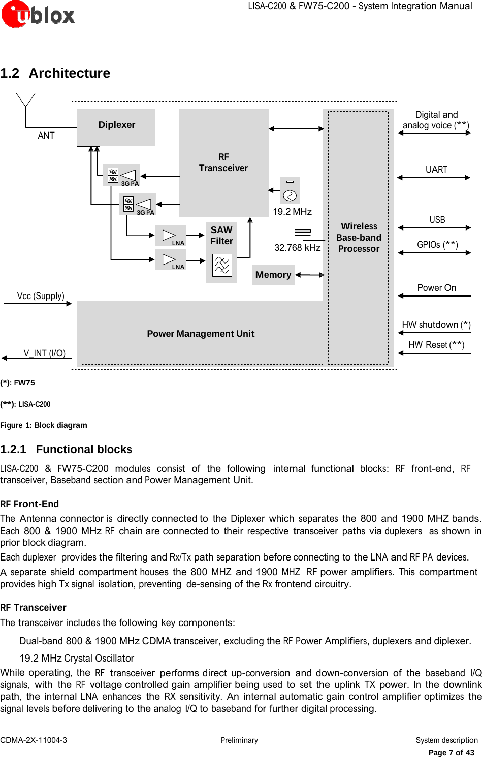
![LISA-C200&FW75-C200-System IntegrationManualCDMA-2X-11004-3 PreliminarySystem descriptionPage 8 of 43 In all the modes, Tx & Rx RF synthesizers are an on-chip voltage controlled oscillator are used to generate the local oscillator signal. The frequency reference to RF synthesizers are provided by a free running 19.2 MHz XO. The Rx path locks and tracks to the base station carrier. An learning algorithm is implemented to capture the temperature characteristic of the xtal, comparing the XO and carrier frequencies, while measuring the thermistor in close proximity to the crystal oscillator. A lookup table is saved over temperature and time. The known frequency difference of the free running crystal oscillator is corrected in the baseband processor enabling quick acquisition. Baseband section and power management unit Another shielding section includes all the digital circuitry and the power supplies, basically the following functional blocks: Wireless baseband processor, a mixed signal ASIC which integrates: Microprocessor for controller functions, CDMA upper layer software ARM9 coprocessor and HW accelerator for CDMA Layer 1 control software and routines Dedicated HW for peripherals control, as UART, USB, etc Memory system in a Multi-Chip Package (MCP) integrating two devices: NOR flash non-volatile memory DDR SRAM volatile memory Power Management Unit (PMU), used to derive all the system supply voltages from the module supply VCC 1.3 Pin description Table 2 provides a summary of the module pin names and descriptions. For the exact specification including pin numbering and additional information see the LISA-C200 Data Sheet [1] or the FW75-C200 Data Sheet [2]. Name Module Power domain I/O Description Remarks VCC All VCC - Module supply Module supply input V_INT FW75-C200 - O Digital I/O Interfaces supply V_INT = 2.85V (typical) generated by the module outputwhen it isswitched-on and the RESET_N(externalresetinput pin) is not forced to the low level.V_INT = 1.8V (typical) generated by the module LISA-C200 - O Digital I/O Interfaces supply output when it isswitched-on and the RESET_N(externalreset input pin) is not forced to the low level. PWR_ON All POS I Power-on input PWR_ON pin has Internal pull-up resistor. GPIO1..10 LISA-C200 GDI I/O GPIO GPIO6..10 Reserved. RESET_N LISA-C200 ERS I External reset input RESET_N pin has Internal pull-up resistor. HW_SHUTDOWN FW75-C200 ERS I External Shutdown input HW_SHUTDOWN pin has Internal pull-up resistor. ANT All ANT - I/O RF antenna STATUS FW75-C200 GDI O LED Indicator Indicated by buffered External LED : Off – Not Powered On – Powered, associated, and authenticated but not transmitting or receiving. Slow Blink but not associated or authenticated; searching. Intermittent Blink - activity proportional to transmitting/receiving speed. For voice applications, turning off and on the intermittent blink based on the ring pulse cycle can indicate a ring event.](https://usermanual.wiki/u-blox-San-Diego/LISAC200A.Users-Manual/User-Guide-1864736-Page-8.png)
![LISA-C200&FW75-C200-System IntegrationManualCDMA-2X-11004-3 PreliminarySystem descriptionPage 9 of 43 Name Module Power domain I/O Description Remarks RI CTS RTS LISA-C200 FW75-C200 LISA-C200 FW75-C200 LISA-C200 FW75-C200 GDI O UART ring indicator Circuit 125 (RI) in ITU-T V.24. Value at internal reset: T/PU. Use to wake up host processor. The output signal is active low. Internal active pull-up to 1.8 V. Internal active pull-up to 2.85 V GDI O UART clear to send Circuit 106 (CTS) in ITU-T V.24. Internal active pull-up to 1.8 V. Internal active pull-up to 2.85 V. GDI I UART ready to send Circuit 105 (RTS) in ITU-T V.24. Internal passive pull-up to 1.8 V. Internal passive pull-up to 2.85 V. GDI O UART received data Circuit 104 (RxD) in ITU-T V.24. RXD LISA-C200 FW75-C200 TXD LISA-C200 FW75-C200 Internal active pull-up to 1.8 V. Internal active pull-up to 2.85 V. GDI I UART transmitted data Circuit 103 (TxD) in ITU-T V.24. Internal passive pull-up to 1.8 V. Internal passive pull-up to 2.85 V. VUSB_DET All USB I USB detect input Input for VBUS (5 V typical) USB supply sense. USB_D- All USB I/O USB Data Line D- 90 nominal differential impedance. Pull-up or pull-down resistors and external series resistors as required by the USB 2.0 high-speed specification [9] are part of the USB pad driver and need not be provided externally. USB_D+ All USB I/O USB Data Line D+ 90 nominal differential impedance. Pull-up or pull-down resistors and external series resistors as required by the USB 2.0 high-speed specification [9] are part of the USB pad driver and need not be provided externally. MIC_N LISA-C200 AUDIO I Differential analog audio input (negative) MIC_P LISA-C200 AUDIO I Differential analog audio input (positive) SPK_P LISA-C200 AUDIO O Differential analog audio output (positive) SPK_N LISA-C200 AUDIO O Differential analog audio output (negative) Differential analog microphone input. Internal DC blocking 0.1 µF capacitor. Differential analog microphone input. Internal DC blocking 0.1 µF capacitor. Differential analog audio output shared for all path modes: earpiece, headset and loudspeaker mode. Differential analog audio output shared for all path modes: earpiece, headset and loudspeaker mode. PCM_SYNC LISA-C200 GDI O Digital Sync Digital Audio Sync pulse. PCM_DO LISA-C200 GDI O Data Output Digital Audio Output. PCM_CLK LISA-C200 GDI O Clock Output Digital Audio Clock Output. PCM_DI LISA-C200 GDI I Data Input Digital Audio Input. SCL LISA-C200 DDC O I2C bus clock line Fixed open drain. No internal pull-up. Value at internal reset: T. SDA LISA-C200 DDC I/O I2C bus data line Fixed open drain. No internal pull-up. Value at internal reset: T. SIM_CLK All SIM O SIM clock Value at internal reset: L. SIM_IO All SIM I/O SIM data Internal 4.7 k pull-up resistor to VSIM. Value at internal reset: L/PD. SIM_RST All SIM O SIM reset Value at internal reset: L. VSIM ALL - O SIM supply output 1.80 V typical or 2.90 V typical generated by the module according to the SIM card type. SIM_GND FW75-C200 SIM O SIM GROUND RSVD All RSVD - RESERVED pin Unless otherwise specified, leave unconnected. GND All GND - Ground All GND pads must be connected to ground. Table 2: Pin description summary](https://usermanual.wiki/u-blox-San-Diego/LISAC200A.Users-Manual/User-Guide-1864736-Page-9.png)
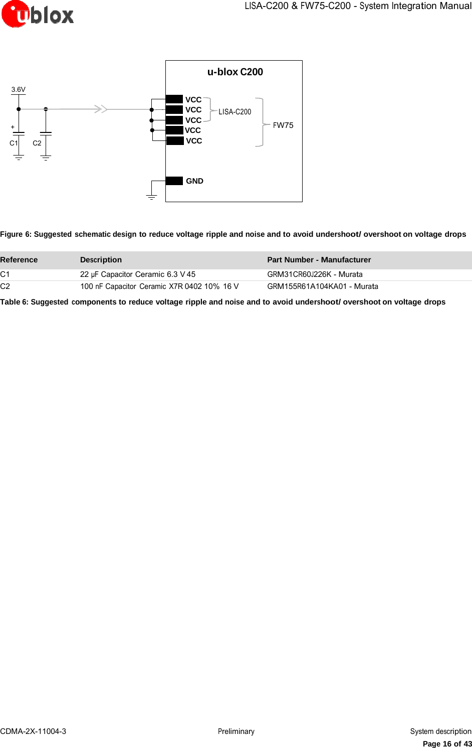
![LISA-C200&FW75-C200-System IntegrationManualCDMA-2X-11004-3 PreliminarySystem descriptionPage 11 of 43The VCC pins are directly connected to the RF power amplifiers and to the integrated Power Management Unit (PMU) within the module: all supply voltages needed by the module are generated from the VCC supply by integrated voltage regulators. When a 1.8 V or a 3 V SIM card type is connected, LISA-C200 & FW75-C200 modules automatically supply the SIM card via the VSIM pin. Activation and deactivation of the SIM interface with automatic voltage switch from 1.8 to 3 V is implemented, in accordance to the ISO-IEC 7816-3 specifications. The 2.8 voltage domain used internally also available on the V_INT pin, to allow more economical and efficient integration of the LISA-C200 & FW75-C200 modules in the final application. The integrated Power Management Unit also provides the control state machine for system start up and system shut down control. 1.4.2 Module supply (VCC) LISA-C200 & FW75-C200 modules must be supplied through the VCC pins by a DC power supply. Voltages must be stable: during operation, the current drawn from VCC can vary by some orders of magnitude. Name Description Remarks VCC Module power supply input VCC pins are internally connected, but all the available pads or pins must be connected to the external supply in order to minimize the power loss due to series resistance. Clean and stable supply is required: low ripple and low voltage drop must be guaranteed. Voltage provided must always be above the minimum limit of the operating range. GND Ground GND pins are internally connected but a good (low impedance) external ground can improve RF performance: all available pads or pins must be connected to ground. Table 3: Module supply pins Higher ESD protection level can be required if VCC is externally accessible on the application board. Higher protection level can be achieved by mounting an ESD protection (e.g. EPCOS CA05P4S14THSG varistor array) on the line connected to this pin. The voltage provided to the VCC pins must be within the normal operating range limits as specified in the LISA-C200 Data Sheet [1] or FW75-C200 Data Sheet [2]. Complete functionality of the module is only guaranteed within the specified minimum and maximum VCC voltage operating range. Ensure that the input voltage at the VCC pins never drops below the minimum limit of the operating range when the module is switched on. Operation above the operating range maximum limit is not recommended and extended exposure beyond it may affect device reliability. Stress beyond the VCC absolute maximum ratings can cause permanent damage to the module: if necessary, voltage spikes beyond VCC absolute maximum ratings must be restricted to values within the specified limits by using appropriate protection. When designing the power supply for the application, pay specific attention to power losses and transients. The DC power supply must be able to provide a voltage profile to the VCC pins with the following characteristics: Voltage drop during transmission must be lower than 250 mV 2 FW75-C200.](https://usermanual.wiki/u-blox-San-Diego/LISAC200A.Users-Manual/User-Guide-1864736-Page-11.png)
![CDMA-2X-11004-3 PreliminarySystem descriptionPage 17 of 43LISA-C200&FW75-C200-System IntegrationManual1.4.3 Current consumption profiles During operation, the current drawn by the LISA-C200 & FW75-C200 modules through the VCC pins can vary by several orders of magnitude. This ranges from continuous high current drawn in CDMA connected mode, to the low current consumption during in idle mode. 1.4.3.1 CDMA connected mode During a CDMA connection, the module can transmit and receive continuously due to the Frequency Division Duplex (FDD) mode of operation with the Code Division Multiple Access (CDMA). The current consumption depends again on output RF power, which is always regulated by network commands. These power control commands are logically divided into a slot of 1.25 ms, thus the rate of power change can reach a maximum rate of 800 Hz. Since transmission and reception are continuously enabled due to FDD CDMA implemented in the 3G that differs from the TDMA implemented in the 2G case. In the worst scenario, corresponding to a continuous transmission and reception at maximum output power (approximately 250 mW or 24 dBm), the current dra wn by the module at the VCC pins is in the order of continuous 600-700 mA. Even at lowest output RF power (approximately 0.01 µW or -50 dBm), the current is in the order of less than 100 mA due to module baseband processing and transceiver activity. An example of current consumption profile of the data module in CDMA continuous transmission mode is shown in Figure 7. Curre nt [mA] 700 610 mA 600 500 400 Depends on TX pow er 300 200 100 <100 mA Not actual data f or illustration 0 1 slot 3G frame Time [ms] Figure 7: VCC current consumption profile versus time during a CDMA connection, with VCC=3.8 V When a packet data connection is established, the actual current profile depends on the amount of transmitted packets; there might be some periods of inactivity between allocated slots where current consumption drops about 100 mA. Alternatively, at higher data rates the transmitted power is likely to increase due to the higher quality signal required by the network to cope with enhanced data speed.](https://usermanual.wiki/u-blox-San-Diego/LISAC200A.Users-Manual/User-Guide-1864736-Page-17.png)
![CDMA-2X-11004-3 PreliminarySystem descriptionPage 18 of 43LISA-C200&FW75-C200-System IntegrationManual1.5 System functions 1.5.1 Module power on The module power on sequence is initiated in one of these ways: Rising edge on the VCC pin to a valid voltage for module supply AND if the PWR_ON pin is permanently low when VCC is applied Falling edge on the PWR_ON pin (pin must be held low for >150 msec) Name Description Remarks PWR_ON Power on input PWR_ON pin has internal pull up resistor. Recommended to use open collector or drain configuration to pull down. Table 7: Power on pin The PWR_ON pin ESD sensitivity rating is 1 kV (Human Body Model according to JESD22-A114F). Higher protection level could be required if the line is externally accessible on the application board. Higher protection level can be achieved by mounting an ESD protection (e.g. EPCOS CA05P4S14THSG varistor array) on the line connected to this pin. 1.5.1.1 Rising edge on VCC \When a supply is connected to VCC pins, the module supply supervision circuit controls the subsequent activation of the power up state machines: the module is switched on when the voltage rises up to the VCC operating range minimum limit (3.4 V) starting from a voltage value lower than 2.25 V (See LISA-C200 Data Sheet [1] or the FW75-C200 Data Sheet [2]), provided that the PWR_ON pin is permanently low when VCC is applied. 1.5.1.2 Falling edge on PWR_ON The module power on sequence starts when a falling edge is forced on the PWR_ON input pin. After applying a falling edge, it is suggested to hold a low level on the PWR_ON signal for at least 300 ms to properly switch on the module. The electrical characteristics of the PWR_ON input pin are different from the other digital I/O interfaces: the high and the low logic levels have different operating ranges and the pin is not-tolerant to voltages up to the battery voltage. The detailed electrical characteristics are described in the LISA-C200 Data Sheet [1] or the FW75-C200 Data Sheet [2]. Once the module has been turned on, PWR_ON pin has no effect. On the other hand it makes no sense to keep this pin low once the module has been turned on: if the pin is kept low it will draw unnecessary current. Following are some typical examples of application circuits to turn the module on using the PWR_ON input pin. The simplest way to turn on the module is to use a push button that shorts the PWR_ON pin to ground. If the PWR_ON input is connected to an external device (e.g. application processor), it is suggested to use an open drain output on the external device.](https://usermanual.wiki/u-blox-San-Diego/LISAC200A.Users-Manual/User-Guide-1864736-Page-18.png)
![CDMA-2X-11004-3 PreliminarySystem descriptionPage 19 of 43LISA-C200&FW75-C200-System IntegrationManualu-blox C200 Power-on push button ESD PWR_ON Application Processor u-blox C200 Open Drain Output PWR_ON Figure 8: PWR_ON application circuits using a push button and an open drain output of an application processor Reference Description Remarks ESD CT0402S14AHSG - EPCOS Varistor array for ESD protection Table 8: Example of pull-up resistor and ESD protection for the PWR_ON application circuits 1.5.1.3 Additional considerations The module is switched on when the voltage rises up to the VCC operating range: the first time that the module is used, it is switched on in this way. Then, the proper way to switch off the module is by means of the AT+CPWROFF command. When the module is in power-off mode, i.e. the AT+CPWROFF command has been sent and a voltage value within the operating range limits is still provided to the VCC pin, the digital input- output pads of the baseband chipset (i.e. all the digital pins of the module) are locked in tri-state (i.e. floating). The power down tri-state function isolates the module pins from its environment, when no proper operation of the outputs can be guaranteed. The module can be switched on from power-off mode by forcing a proper start-up event (i.e. a falling edge on the PWR_ON pin). After the detection of a start-up event, all the digital pins of the module are held in tri-state until all the internal LDO voltage regulators are turned on in a defined power-on sequence. Then, as described in Datasheet the baseband core is still held in reset state for a time interval: the internal reset signal (which is not available on a module pin) is still low and any signal from the module digital interfaces is held in reset state. The reset state of all the digital pins is reported in the pin description table of the LISA-C200 Data Sheet [1] or the FW75-C200 Data Sheet [2]. When the internal signal is released, the configuration of the module interfaces starts: during this phase any digital pin is set in a proper sequence from the reset state to the default operational configuration. Finally, the module is fully ready to operate when all interfaces are configured. The Internal Reset signal is not available on a module pin.](https://usermanual.wiki/u-blox-San-Diego/LISAC200A.Users-Manual/User-Guide-1864736-Page-19.png)
![CDMA-2X-11004-3 PreliminarySystem descriptionPage 20 of 43LISA-C200&FW75-C200-System IntegrationManual1.5.2 Module power off The correct way to switch off LISA-C200 & FW75-C200 modules is by means of +CPWROFF AT command (more details in u-blox C200 AT Commands Manual [3]): in this way the current parameter settings are saved in the module’s non-volatile memory and a proper network detach is performed. An under-voltage shutdown will be done if the VCC supply is removed, but in this case the current parameter settings are not saved in the module’s non-volatile memory and a proper network detach cannot be performed. 1.5.3 Module reset The module reset can be performed: Forcing a low level on the RESET_N input pin, causing an “external” or “hardware” reset (LISA-C200 only) AT+CFUN command (more details in u-blox C200 AT Commands Manual [3]): in this case an “internal” or “software” reset is performed, causing an asynchronous reset of the baseband processor 1.6 RF connection The ANT connector has 50 nominal characteristic impedance and must be connected to the antenna through a 50 transmission line to allow transmission and reception of radio frequency (RF) signals in the Cell and PCS operating bands. Name Description Remarks ANT FW75 LISA-C200 RF connector Zo = 50 nominal characteristic impedance. U.FL connector Surface Mount pad Table 9: Antenna connector The ANT port ESD immunity rating is 500 V (according to IEC 61000-4-2). Higher protection level could be required if the line is externally accessible on the application board. Choose an antenna with optimal radiating characteristics for the best electrical performance and overall module functionality. Focus on minimizing the insertion loss between radiating antenna and the module RF connector. Overall system performance depends on antenna reception and transmission. See section 2.4 for further details regarding antenna guidelines.](https://usermanual.wiki/u-blox-San-Diego/LISAC200A.Users-Manual/User-Guide-1864736-Page-20.png)
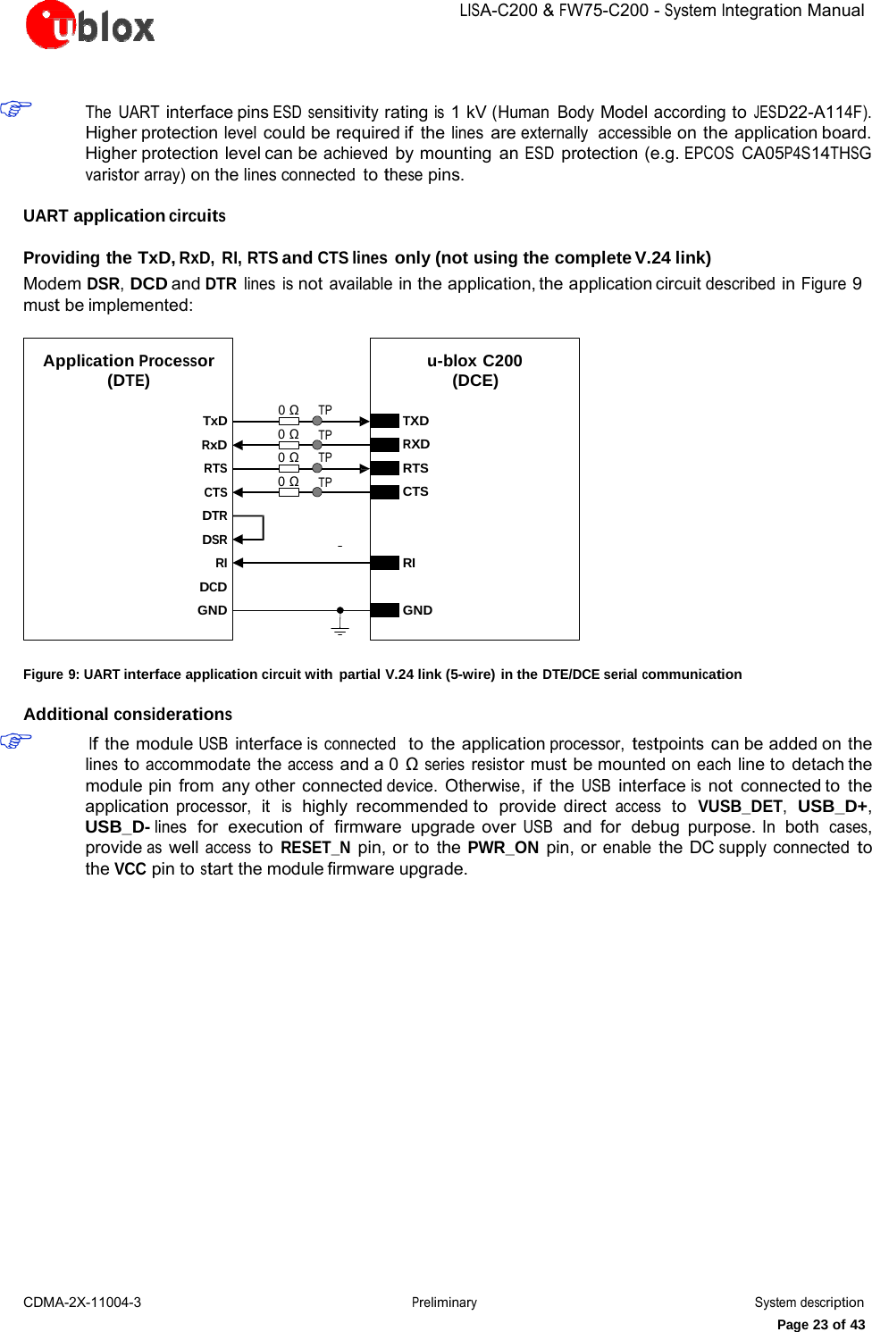
![CDMA-2X-11004-3 PreliminarySystem descriptionPage 21 of 43LISA-C200&FW75-C200-System IntegrationManual1.7 Serial communication LISA-C200 & FW75-C200 modules provide the following serial communication interfaces where AT command interface and Packet-Switched Data communication are concurrently available: One asynchronous serial interface (UART) that provides RS-232 functionality conforming to ITU-T V.24 Recommendation [4], with limited data rate. One full-speed USB 2.0 compliant interface, with maximum data rate of 12 Mb/s. Only one interface is active. Default is USB, if no USB is detected then it is assumed that the UART interface is desired. LISA-C200 & FW75-C200 modules are designed to operate as a CDMA wireless modem, which represents the data circuit-terminating equipment (DCE) as described by the ITU-T V.24 Recommendation [4]. A customer application processor connected to the module through one of the interfaces represents the data terminal equipment (DTE). All the interfaces listed above are controlled and operated with: Sprint required AT Commands Verizon required AT Commands AT commands according to 3GPP TS 27.010 [7] AT commands according to 3GPP TS 27.005 [6] AT commands according to 3GPP TS 27.010 u-blox AT commands For the complete list of supported AT commands and their syntax refer to the u-blox C200 AT Commands Manual [3]. The USB interface, using all the lines provided (VUSB_DET, USB_D+ and USB_D-), can be used for firmware upgrade: To directly enable PC (or similar) connection to the module for firmware upgrade, provide direct access on the application board to the VUSB_DET, USB_D+ and USB_D- lines of the module . Also provide access to the PWR_ON & HW_SHUTDOWN pins, or enable the DC supply connected to the VCC pin to start the module firmware upgrade The following sub-chapters describe serial interface configuration and provide a detailed description of each interface for the application circuits. 1.7.1 Serial interfaces configuration UART and USB serial interfaces are available as AT command interface and for Packet-Switched Data communication. The serial interfaces are configured as described in Table 10 (for information about further settings, please refer to the u-blox C200 AT Commands Manual [3]). Note : The UART is 5 wire implementation therefore DTR, DSR and DCD functions are not available.](https://usermanual.wiki/u-blox-San-Diego/LISAC200A.Users-Manual/User-Guide-1864736-Page-21.png)
![CDMA-2X-11004-3 PreliminarySystem descriptionPage 22 of 43LISA-C200&FW75-C200-System IntegrationManualInterface AT Settings Comments UART interface Enabled Multiplexing mode can be enabled by AT+CMUX command providing following channels: Channel 0: control channel Channel 1: AT commands Channel 2: data connection AT+IPR=115200 Baud rate: 115200 b/s AT+ICF=0,0 Frame format: 8 bits, no parity, 1 stop bit USB interface Enabled Table 10: Default serial interfaces configuration 1.7.2 Asynchronous serial interface (UART) The UART interface is a 5-wire unbalanced asynchronous serial interface that provides AT commands interface and PSD data communication. UART interface provides RS-232 functionality conforming to the ITU-T V.24 Recommendation (more details available in ITU Recommendation [4]), with CMOS compatible signal levels: 0 V for low data bit or ON state, and 2.8 V for high data bit or OFF state. One external voltage translators (e.g. Maxim MAX13234E) could be used to provide RS-232 (5 lines) compatible signal levels. This chip translates the voltage levels from 1.8 V (module side) to the RS-232 standard. For detailed electrical characteristics refer to LISA-C200 Data Sheet [1] or the FW75- C200 Data Sheet [2]. FW75-C200 logic levels are 2.8 V interface. LISA-C200 logic levels are 1.8 V interface. The LISA-C200 & FW75-C200 modules are designed to operate as a CDMA wireless modem, which represents the data circuit-terminating equipment (DCE) as described by the ITU-T V.24 Recommendation [4]. A customer application processor connected to the module through the UART interface represents the data terminal equipment (DTE). The signal names of the LISA-C200 & FW75-C200 modules UART interface conform to the ITU-T V.24 Recommendation [4]. UART interfaces include the following lines: Name Description Remarks RI Ring Indicator Module output RTS Ready to send Module hardware flow control input Circuit 105 (Request to send) in ITU-T V.24 FW75 - Internal active pull-up to V_INT (2.8 V) interface. LISA-C200- Internal active pull-up to V_INT (1.8 V) interface. CTS Clear to send Module hardware flow control output Circuit 106 (Ready for sending) in ITU-T V.24 FW75-C200 - Internal active pull-up to V_INT (2.8 V) interface. LISA-C200- Internal active pull-up to V_INT (1.8 V) interface. TxD Transmitted data Module data input Circuit 103 (Transmitted data) in ITU-T V.24 Internal active pull-up to V_INT (2.8 V) enabled. FW75-C200- Internal active pull-up to V_INT (2.8 V) interface. LISA-C200- Internal active pull-up to V_INT (1.8 V) interface. RxD Received data Module data output Circuit 104 (Received data) in ITU-T V.24 FW75-C200- Internal active pull-up to V_INT (2.8 V) interface. LISA-C200- Internal active pull-up to V_INT (1.8 V) interface. GND Ground Table 11: UART interface signals](https://usermanual.wiki/u-blox-San-Diego/LISAC200A.Users-Manual/User-Guide-1864736-Page-22.png)
![CDMA-2X-11004-3 PreliminarySystem descriptionPage 24 of 43LISA-C200&FW75-C200-System IntegrationManual1.7.3 USB interface LISA-C200 & FW75-C200 modules provide a full-speed USB interface at 12 Mb/s compliant with the Universal Serial Bus Revision 2.0 specification [9]. It acts as a USB device and can be connected to any USB host such as a PC or other Application Processor. The USB-device shall look for all upper-SW-layers like any other serial device. This means that LISA-C200 & FW75-C200 modules emulate all serial control logical lines. If the logical DTR line isn't enabled by the USB host, the module doesn’t answer to AT commands by the USB interface. Name Description Remarks VUSB_DET USB detect input Apply 5 V typical to enable USB USB_D+ USB Data Line D+ 90 nominal differential impedance. Pull-up or pull-down resistors and external series resistors as required by the USB 2.0 high-speed specification [9] are part of the USB pad driver and need not be provided externally. USB_D- USB Data Line D- 90 nominal differential impedance. Pull-up or pull-down resistors and external series resistors as required by the USB 2.0 high-speed specification [9] are part of the USB pad driver and need not be provided externally. Table 12: USB pins The USB interface pins ESD sensitivity rating is 1 kV (Human Body Model according to JESD22-A114F). Higher protection level could be required if the lines are externally accessible on the application board. Higher protection level can be achieved by mounting a very low capacitance (i.e. less or equal to 1 pF) ESD protection (e.g. Tyco Electronics PESD0402-140 ESD protection device) on the lines connected to these pins. LISA-C200 & FW75-C200 module identifies itself by its VID (Vendor ID) and PID (Product ID) combination, included in the USB device descriptor. VID and PID of LISA-C200 & FW75-C200 modules are the following: VID = 0x1546 PID = 0x1121 1.7.3.1 USB application circuit Since the module acts as a USB device, the USB supply (5.0 V typ.) must be provided to VUSB_DET by the connected USB host. The USB interface is enabled only when a valid voltage as USB supply is detected by the VUSB_DET input. Neither the USB interface, nor the whole module is supplied by the VUSB_DET input: the VUSB_DET senses the USB supply voltage and absorbs few microamperes. The USB_D+ and USB_D- lines carry the USB serial data and signaling. The lines are used in single ended mode for relatively low speed signaling handshake, as well as in differential mode for fast signaling and data transfer. USB pull-up or pull-down resistors on pins USB_D+ and USB_D- as required by the Universal Serial Bus Revision 2.0 specification [9] are part of the USB pad driver and do not need to be externally provided. External series resistors on pins USB_D+ and USB_D- as required by the Universal Serial Bus Revision 2.0 specification [9] are also integrated: characteristic impedance of USB_D+ and USB_D- lines is specified by the USB standard. The most important parameter is the differential characteristic impedance applicable for odd-mode electromagnetic field, which should be as close as possible to 90 differential: signal integrity may be degraded if the PCB layout is not optimal, especially when the USB signaling lines are very long.](https://usermanual.wiki/u-blox-San-Diego/LISAC200A.Users-Manual/User-Guide-1864736-Page-24.png)
![CDMA-2X-11004-3 PreliminarySystem descriptionPage 25 of 43LISA-C200&FW75-C200-System IntegrationManualUSB DEVICE CONNECTOR u‐bloxC200VBUS VUSB_DET D+ USB_D+ D- USB_D- GND D1 D2 D3 C1 GND Figure 10: USB Interface application circuit Reference Description Part Number - Manufacturer D1, D2, D3 Very Low Capacitance ESD Protection PESD0402-140 - Tyco Electronics C2 100 nF Capacitor Ceramic X7R 0402 10% 16 V GRM155R61A104KA01 - Murata Table 13: Component for USB application circuit If the USB interface is not connected to the application processor, it is highly recommended to provide direct access to the VUSB_DET, USB_D+, USB_D- lines for execution of firmware upgrade over USB and for debug purpose: testpoints can be added on the lines to accommodate the access. Provide access to RESET_N pin, or to the PWR_ON pin, or enable the DC supply connected to the VCC pin to start the module firmware upgrade If the USB interface is not used, the USB_D+, USB_D- and VUSB_DET pins can be left unconnected, but it is highly recommended to provide direct access to the lines for execution of firmware upgrade and for debug purpose. 1.7.4 MUX Protocol (3GPP 27.010) LISA-C200 & FW75-C200 modules have a software layer with MUX functionality, 3GPP TS 27.010 Multiplexer Protocol [7], available on the UART physical link. The USB interface doesn’t support the multiplexer protocol. This is a data link protocol (layer 2 of OSI model) which uses HDLC-like framing and operates between the module (DCE) and the application processor (DTE) and allows a number of simultaneous sessions over the UART: the user can concurrently use AT command interface on one MUX channel and Packet-Switched Data communication on another MUX channel.. Each session consists of a stream of bytes transferring various kinds of data such as SMS, PSD, AT commands in general. This permits, for example, SMS to be transferred to the DTE when a data connection is in progress. The following virtual channels are defined: Channel 0: control channel Channel 1: AT commands Channel 2: data connection 1.8 Reserved pins (RSVD) LISA-C200 & FW75-C200 modules have pins reserved for future use. All the RSVD pins/pads must be left unconnected on the application board.](https://usermanual.wiki/u-blox-San-Diego/LISAC200A.Users-Manual/User-Guide-1864736-Page-25.png)
![LISA-C200&FW75-C200-System IntegrationManualCDMA-2X-11004-3 PreliminaryDesign-InPage 28 of 432 Design-In 2.1 Design-in checklist 2.1.1 Schematic checklist The following are the most important points for a simple schematic check: DC supply must provide a nominal voltage at VCC pin above the minimum operating range limit. DC supply must be capable of supporting 1.2 A, providing a voltage at VCC pin above the minimum operating range limit and with a maximum 250 mV voltage drop from the nominal value. VCC supply should be clean, with very low ripple/noise: suggested passive filtering parts can be inserted. Connect only one DC supply to VCC: different DC supply systems are mutually exclusive. Don’t apply loads which might exceed the limit for maximum available current from V_INT supply. Check that voltage level of any connected pin does not exceed the relative operating range. Capacitance and series resistance must be limited on each SIM signal to match the SIM specifications. Insert the suggested low capacitance ESD protection and passive filtering parts on each SIM signal. Check UART signals direction, since the signal names follow the ITU-T V.24 Recommendation [4]. Provide appropriate access to USB interface and/or to UART RxD, TxD lines and access to PWR_ON and/or HW_SHUTDOWN lines on the application board in order to flash/upgrade the module firmware. Provide appropriate access to USB interface and/or to UART RxD, TxD, CTS, RTS lines for debugging. Add a proper pull-up resistor to a proper supply on each DDC (I2C) interface line, if the interface is used. Capacitance and series resistance must be limited on each line of the DDC interface. Use transistors with at least an integrated resistor in the base pin or otherwise put a 10 k resistor on the board in series to the GPIO when those are used to drive LEDs. Insert the suggested passive filtering parts on each used analog audio line. Provide proper precautions for ESD immunity as required on the application board. All unused pins can be left floating on the application board Layout checklist The following are the most important points for a simple layout check: Check 50 nominal characteristic impedance of the RF transmission line connected to ANT coax connector or Printed Circuit Board 50 transmission line impedance for LISA-C200 Follow the recommendations of the antenna producer for correct antenna installation and deployment. Ensure no coupling occurs with other noisy or sensitive signals (primarily SIM signals). VCC line should be wide and short. Ensure proper grounding. Consider “No-routing” areas for the Data Module footprint. Optimize placement for minimum length of RF line and closer path from DC source for VCC. Design USB_D+ / USB_D- connection as 90 differential pair. 2.1.2 Antenna checklist Antenna should have 50 impedance, V.S.W.R less then 3:1, recommended 2:1 on operating bands in deployment geographical area. Follow the recommendations of the antenna producer for correct antenna installation and deployment (PCB layout and matching circuitry).](https://usermanual.wiki/u-blox-San-Diego/LISAC200A.Users-Manual/User-Guide-1864736-Page-28.png)
![LISA-C200&FW75-C200-System IntegrationManualCDMA-2X-11004-3 PreliminaryDesign-InPage 31 of 432.3 Design Guidelines The following design guidelines must be met for optimal integration of LISA-C200 module on the final application board. 2.3.1 Layout guidelines per pin function This section groups the u-blox C200 module pins by signal function and provides a ranking of importance in layout design. See 1: FW75-C200 2: LISA-C200 Table 17 for a list of pins ranked by their importance in layout design. See the LISA-C200 Data Sheet [1] or the FW75 Data Sheet [2] for the complete pin lists. Rank Function Pin(s) Layout Remarks 1st RF Connector 2nd Main DC Supply 3rd USB Signals ANT VCC USB_D+ USB_D- Very Important Design for 50 characteristic impedance. Very Important VCC line should be wide and short. Route away from sensitive analog signals. Very Important Route USB_D+ and USB_D- as differential lines: design for 90 differential impedance. 4th Ground GND Careful Layout Provide proper grounding. 5th Sensitive Pin : Careful Layout Avoid coupling with noisy signals. Power On HW_SHUTDOWN 6th Digital pins and supplies: PWR_ON HW_SHUTDOWN Common Practice Follow common practice rules for digital pin routing. SIM Card Interface VSIM, SIM_CLK, SIM_IO, SIM_RST UART TXD, RXD, CTS, RTS, RI External Reset HW_SHUTDOWN1 RESET_N2 General Purpose I/O2 GPIO1, GPIO2, GPIO3, GPIO4, GPIO5 USB detection VUSB_DET Supply for Interfaces V_INT 1: FW75-C200 2: LISA-C200 Table 17: Pin list in order of decreasing importance for layout design](https://usermanual.wiki/u-blox-San-Diego/LISAC200A.Users-Manual/User-Guide-1864736-Page-31.png)
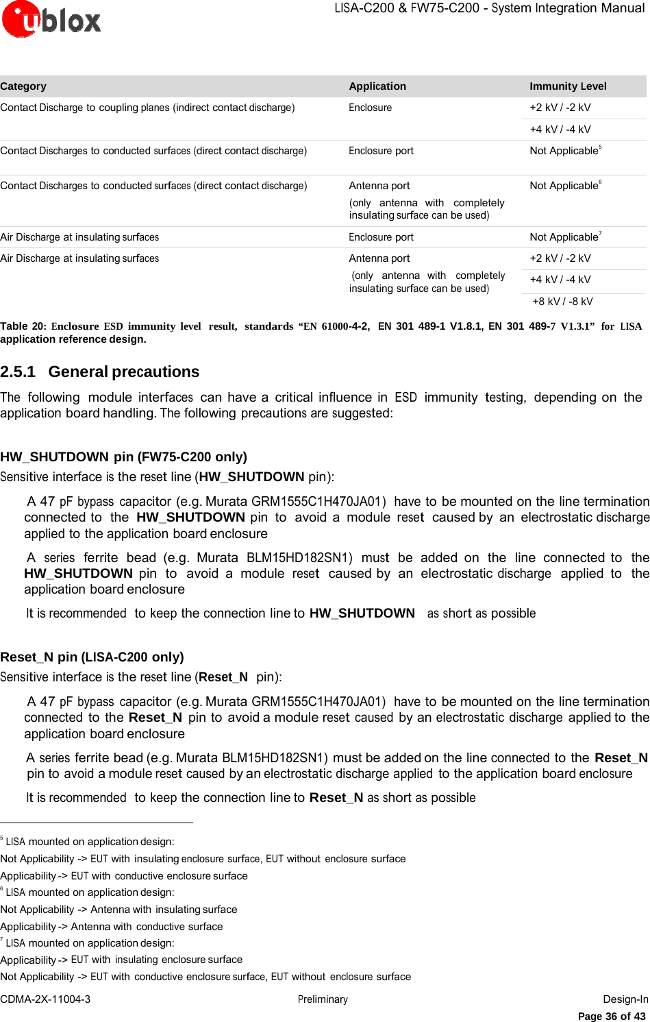
![LISA-C200&FW75-C200-System IntegrationManualCDMA-2X-11004-3 PreliminaryDesign-InPage 35 of 43For good antenna radiation performance, antenna dimensions should be comparable to a quarter of the wavelength. Different antenna types can be used for the module, many of them (e.g. patch antennas, monopole) are based on a resonating element that works in combination with a ground plane. The ground plane, ideally infinite, can be reduced down to a minimum size that must be similar to one quarter of the wavelength of the minimum frequency that has to be radiated (transmitted/received). Numerical sample: frequency = 1 GHz wavelength = 30 cm minimum ground plane (or antenna size) = 7.5 cm. Below this size, the antenna efficiency is reduced. 2.5 ESD immunity test precautions The immunity of the device (i.e. the application board where LISA-C200 & FW75-C200 module is mounted) Electrostatic Discharge must be certified in compliance to the testing requirements standard [12], and the requirements for radio and digital cellular radio telecommunications system equipment standards [12] and [14]. The ESD test is performed at the enclosure port referred to as the physical boundary through which the EM field radiates. If the device implements an integral antenna, the enclosure port is seen as all insulating and conductive surfaces housing the device. If the device implements a removable antenna, the antenna port can be separated from the enclosure port. The antenna port comprises the antenna element and its interconnecting cable surfaces. The applicability of the ESD test depends on the device classification, as well the test on other ports or on interconnecting cables to auxiliary equipments depends to the device accessible interfaces and manufacturer requirements. Contact discharges are performed at conductive surfaces whereas air discharges are performed on insulating surfaces. Indirect contact discharges are performed on the measurement setup horizontal and vertical coupling planes. Implement the following precautions to satisfy ESD immunity test requirements performed at the device enclosure in compliance to the category level and shown in the following table. Application Category Immunity Level All exposed surfaces of the radio equipment and ancillary equipment in a representative configuration Contact Discharge 4 kV Air Discharge 8 kV Table 19: Electromagnetic Compatibility (EMC) ESD immunity requirement, standards “EN 61000-4-2, EN 301 489-1 V1.8.1, EN 301 489-7 V1.3.1” Although EMC certification (including ESD immunity testing) must be performed in the final application of the radio equipment EUT, results are provided for LISA modules performing the test with a representative configuration to show that requirements can be met. Since an external antenna is used, the antenna port can be separated from the enclosure port. The reference application is not enclosed in a box so the enclosure port is not indentified with physical surfaces. Therefore, some test cases cannot be applied. Only the antenna port is identified as accessible for direct ESD exposure. The reference application implements all precautions described in the sections below. ESD immunity test results and applicability are reported in Table 20 according to test requirements [12], [12] and [14].](https://usermanual.wiki/u-blox-San-Diego/LISAC200A.Users-Manual/User-Guide-1864736-Page-35.png)
![LISA-C200&FW75-C200-System IntegrationManualCDMA-2X-11004-3 PreliminaryDesign-InPage 38 of 43 If the device implements an external antenna and the antenna or its connecting cable are not provided with completely insulating enclosure to avoid air discharge up to +8 kV / -8 kV to the whole antenna and cable surfaces, the following precautions to ESD immunity test should be implemented on the application board A higher protection level is required at the ANT port if the line is externally accessible on the application board. ESD immunity test requires protection up to +4 kV / -4 kV for direct Contact Discharge and up to +8 kV / -8 kV for Air Discharge applied to the antenna port. 2.5.3 Module interfaces precautions All the module pins that are externally accessible should be included in the ESD immunity test since they are considered to be a port as defined in [12]. Depending on applicability, and in order to satisfy ESD immunity test requirements and ESD category level, pins connected to the port should be protected up to +4 kV / -4 kV for direct Contact Discharge, and up to +8 kV / -8 kV for Air Discharge applied to the enclosure surface. The maximum ESD sensitivity rating of all the pins of the module, except the ANT pin, is 1 kV (Human Body Model according to JESD22-A114F). A higher protection level can be achieved by mounting an ESD protection (e.g. EPCOS CA05P4S14THSG varistor array or CT0402S14AHSG). For the USB interface a very low capacitance (i.e. less or equal to 1 pF) ESD protection (e.g. Tyco Electronics PESD0402-140 ESD protection device) can be mounted on the lines connected to USB_D+ and USB_D- pins. For the SIM interface a low capacitance (i.e. less than 10 pF) ESD protection (e.g. Infineon ESD8V0L2B-03L or AVX USB0002) must be placed near the SIM card holder on each line (VSIM, SIM_IO, SIM_CLK, SIM_RST).](https://usermanual.wiki/u-blox-San-Diego/LISAC200A.Users-Manual/User-Guide-1864736-Page-38.png)
![LISA-C200&FW75-C200-System IntegrationManualCDMA-2X-11004-3 PreliminaryRelated documentsPage 42 of 43Related documents [1] LISA-C200 Data Sheet, Docu No CDMA-2X-11001 [2] FW75 Data Sheet, Docu No CDMA-1X-11006 [3] u-blox C200 AT Commands Manual, Docu No CDMA-2X-11002 [4] ITU-T Recommendation V.24, 02-2000. List of definitions for interchange circuits between data terminal equipment (DTE) and data circuit-terminating equipment (DCE). http://www.itu.int/rec/T-REC-V.24-200002-I/en [5] 3GPP TS 27.007 - AT command set for User Equipment (UE) (Release 1999) [6] 3GPP TS 27.005 - Use of Data Terminal Equipment - Data Circuit terminating; Equipment (DTE - DCE) interface for Short Message Service (SMS) and Cell Broadcast Service (CBS) (Release 1999) [7] 3GPP TS 27.010 - Terminal Equipment to User Equipment (TE-UE) multiplexer protocol (Release 1999) [8] 3GPP TS 23.060 - General Packet Radio Service (GPRS); Service description; Stage 2 (Release 1999) [9] Universal Serial Bus Revision 2.0 specification, http://www.usb.org/developers/docs/ [10] I2C-Bus Specification Version 2.1 Philips Semiconductors (January 2000), http://www.nxp.com/acrobat_download/literature/9398/39340011_21.pdf [11] GPS Implementation Application Note, Docu No GSM.G1-CS-09007 [12] CENELEC EN 61000-4-2 (2001): “Electromagnetic compatibility (EMC) - Part 4-2: Testing and measurement techniques - Electrostatic discharge immunity test”. [13] ETSI EN 301 489-1 V1.8.1: “Electromagnetic compatibility and Radio spectrum Matters (ERM); ElectroMagnetic Compatibility (EMC) standard for radio equipment and services; Part 1: Common technical requirements” [14] ETSI EN 301 489-7 V1.3.1 “Electromagnetic compatibility and Radio spectrum Matters (ERM); ElectroMagnetic Compatibility (EMC) standard for radio equipment and services; Part 7: Specific conditions for mobile and portable radio and ancillary equipment of digital cellular radio telecommunications systems (GSM and DCS)“ Some of the above documents can be downloaded from u-blox web-site (http://www.u-blox.com). Revision history Revision Date Name Status / Comments - 11/24/11 rcam Initial Release 1 5/23/2012 smoi Updated product names 2 7/9/2012 smoi Unification of SIM nomenclature 3 8/20/2012 smoi Document status change](https://usermanual.wiki/u-blox-San-Diego/LISAC200A.Users-Manual/User-Guide-1864736-Page-42.png)