u blox San Diego LISAC200A CDMA 1xRTT Cellular Module User Manual
u-blox San Diego, Inc. CDMA 1xRTT Cellular Module Users Manual
Contents
- 1. Users Manual
- 2. Host Unit Manual
Users Manual
locate, communicate,
ac
c
ele
r
a
te
LISA-C200
& FW75-C200
CDMA 1xRTT
Wireless
Modules
System
Integration
Man
ual
Abs
tra
c
t
This
document
describes
the
f
ea
t
ure
s
and the integration
of
u-blox
LISA-C200
and
F
W75-
C
200
CDMA2000
1xRTT
w
ir
e
l
e
ss
modul
e
s
.
These
modul
e
s
are complete and cost efficient CDMA
s
ol
uti
on
s
offering 153 kb/s data
speed
dual-band 800/1900 MHz data
t
r
ans
mi
ss
ion
technology
in
compact
form factors.
www
.u-blox.
c
om

LIS
A
-C200
&
F
W75-
C
200
-
S
yste
m
I
nte
gra
t
ion
Manual
CDMA-2X-11004-3
Page
2of43
Document
Info
rma
t
ion
Title
LISA-C200
&
F
W75-
C
200
Subtitle CDMA
1x
RT
T
Wireless
Mo
dul
e
s
Document type
S
yste
m
I
nte
gra
t
ion
Manual
Document number CDMA-2X-11004-3
Document
st
at
u
s
P
re
limin
a
r
y
Document
st
at
u
s
in
f
orma
t
ion
Objective
S
pe
ci
f
i
ca
t
ion
Advance
I
nfor
ma
t
ion
This
document
c
on
t
a
in
s
target
values. Revised
and
s
uppl
e
me
ntar
y
data will be
publi
s
he
d
later.
This
document
c
on
t
a
in
s
data
based
on
early
t
e
s
t
ing.
Revised
and
s
uppl
e
me
ntar
y
data
w
ill
be
publi
s
he
d
later.
P
r
e
limi
na
r
y
This
document
c
on
t
a
in
s
data from product
verification.
Revised
and
s
uppl
e
me
ntar
y
data
may
be
publi
s
he
d
later.
Released
This
document
c
on
t
a
in
s
the final product
s
pe
ci
f
i
ca
t
ion.
This
document
applie
s
to the following products:
Name Type number
F
ir
mw
are
version
PCN
/
IN
LISA-C200
LI
S
A-
C
200-0
1S
E
0.S
.03.00.10
R
UBX-TN-12041
LISA-C200
LI
S
A-
C
200-2
1S
E
0.V.03
.00.0
2R
UBX-TN-12041
FW75-C200 FW-C200-01S
E
0.S
.03.00.10
R
UBX-TN-12041
FW75-C200 FW-C200-21S
E
0.V.03
.00.0
2R
UBX-TN-12041
This
document and the
use
of
any
information
contained
therein,
is
su
b
je
c
t
to the
a
cc
e
p
t
a
n
c
e
of the u-blox
t
e
r
ms
and
conditions.
T
h
e
y
can be downloaded from
www
.u-b
lox.
c
om.
u-blox
makes
no
w
a
rr
a
n
t
i
e
s
based
on the
accuracy
or
c
ompl
e
t
e
n
e
ss
of the
c
on
t
e
n
t
s
of this document and
reserves
the right to m
a
k e
changes
to
sp
e
c
ific
a
t
ion
s
and product d
e
s
c
r
ipt
ion
s
at any time without notice.
u-blox
reserves
all righ
t
s
to this document and the information contained herein.
R
e
produ
c
t
ion,
use
or
disclosure
to third p
a
r
t
ie
s
wit
hou
t
express permission is
st
r
ic
t
ly
prohibited. Copyright © 2012, u-blox AG.
u-blox® is a
registered
trademark of u-blox Holding AG in the
EU
and other countries.
LIS
A
-C200
&
F
W75-
C
200
-
S
yste
m
I
nte
gra
t
ion
Manual
CDMA-2X-11004-3
P
r
e
limin
a
r
y
P
r
e
f
a
c
e
Page
3 of 43
Prefa
c
e
u-blox
Technical
Documentation
As
part of our commitment to customer
s
upp
ort
,
u-blox maintains an extensive volume of technical
documentation for our
product
s
.
In
addition to our
product-
s
pe
ci
f
i
c
t
e
chn
i
ca
l
data
s
h
ee
t
s
,
the following
ma
nu
a
l
s
are available
to
a
ss
i
s
t
u-blox
cus
t
om
e
r
s
in product
de
s
ign
and development.
AT
Commands
Manual:
This
document
provid
e
s
the
de
s
cr
i
pti
on
of the
s
uppor
t
e
d
AT
co
mm
a
nd
s
by the
LISA-C200
&
F
W75-
C
200
module to
ve
ri
f
y
all
implemented
funct
io
na
li
t
i
e
s
.
System Integration Manual:
This
Manual
prov
i
de
s
hardware
de
s
ign
instructions and information on how
t
o
s
e
t
up production and final product
t
e
s
t
s
.
Application
Note:
document
provi
de
s
general
de
s
ign
in
s
t
ructio
ns
and information that
applies
to all u-blox
Wireless
modul
e
s
.
See
S
e
ction
Re
l
a
t
e
d
d
ocum
e
nt
s
for a
li
s
t
of Application
Notes
related to your
Wir
e
l
e
ss
Module.
How to
use this
M
anual
The
LISA-C200
&
F
W75-
C
200
S
yste
m
I
nte
gra
t
ion
Manual
prov
i
de
s
the
necessary
information to
s
ucce
ss
f
ull
y
de
s
ign
in and configure
t
he
s
e
u-blox
wireless
modul
e
s
.
This manual has
a modular
s
t
ruct
ure
.
I
t
is
not
necessary
to
read
it from the beginning to the end.
The
following
symbols are used
to highlight important information within the manual:
An
index
finger points out
key
information pertaining to module integration and performance.
A warning
s
ymbol
indicates actions
that
could
negatively impact or damage the module.
Qu
est
ion
s
.
I
f
you
have any
qu
e
s
t
ion
s
about u-blox
Wireless
I
nte
gra
t
ion,
pl
ea
s
e
:
Read
thi
s
manual
carefully.
Contact our information
service
on the
homepage
h
tt
p://
ww
w.
u-b
lox
.
c
om
Read
the
qu
e
s
t
io
ns
and
answers
on our
F
A
Q
da
t
a
ba
s
e
on the
homepage
h
tt
p://
ww
w.
u-b
lox.
c
om
Technical
Support
Worldwide
Web
Our website
(www.u-blox.com)
is
a rich pool of information.
P
roduct
information, technical documents and
helpful
FAQ can
be
accessed
24h a day.
By
E
-mail
Contact the
ne
a
r
e
s
t
Technical
S
uppor
t
office by email.
Use
our
service
pool email
addresses
rather than any
pe
r
s
on
a
l
email
address
of our
s
t
a
ff
.
This makes sure
that your
r
e
qu
e
s
t
is processed as
s
oon
as possible.
You
w
ill
find the contact
de
t
a
il
s
at the end of the document.
Helpful Information when
Contacting Technical
Support
When contacting
Technical
S
uppor
t
please have
the following information ready:
Module type
(e.g.
LISA-C200
)
and firmware
ve
r
s
ion
Module configuration
Clear
de
s
cr
i
pt
ion
of your
qu
e
s
t
ion
or the problem
A
s
hor
t
de
s
cr
i
ptio
n
of the application
Your
complete
contact
de
t
a
il
s

LIS
A
-C200
&
F
W75-
C
200
-
S
yste
m
I
nte
gra
t
ion
Manual
CDMA-2X-11004-3
P
r
e
limin
a
r
y
C
on
t
e
n
t
s
Page
4 of 43
Contents
P
re
fa
c
e ................................................................................................................................3
Contents
..............................................................................................................................4
1
S
y
s
te
m
desc
ripti
on .......................................................................................................6
1.1
Overview
.............................................................................................................................................. 6
1.2
Architecture..........................................................................................................................................
7
1.2.1
Functional
bl
ock
s
...........................................................................................................................
7
1.3
Pin
d
e
s
cr
i
ptio
n
...................................................................................................................................... 8
1.4
P
ow
e
r
management
........................................................................................................................... 10
1.4.1
P
ow
e
r
s
uppl
y
circuit
ove
r
vi
e
w
......................................................................................................
10
1.4.2 Module
s
uppl
y
(VCC)
..................................................................................................................
11
1.4.3 Current
c
on
s
um
ptio
n
prof
il
e
s
......................................................................................................
17
1.5
S
yste
m
funct
ion
s
................................................................................................................................ 18
1.5.1 Module power on
.......................................................................................................................
18
1.5.2 Module power off
.......................................................................................................................
20
1.5.3 Module
r
e
s
e
t
...............................................................................................................................
20
1.6
RF
con
ne
ction
..................................................................................................................................... 20
1.7
Serial
communication
......................................................................................................................... 21
1.7.1
Serial
inter
f
ace
s
configuration
.....................................................................................................
21
1.7.2
A
s
ync
hrono
us
serial
interface
(U
A
RT
)
...........................................................................................
22
1.7.3
USB
interface...............................................................................................................................
24
1.7.4 MUX
P
rotocol
(3GPP
27.010) ......................................................................................................
25
1.8
Reserved
pin
s
(RSVD)
.......................................................................................................................... 25
1.9
S
che
ma
t
i
c
for
LISA-C200
and
FW75-C200
modul
e
s
integration
......................................................... 26
1.10
Appr
ova
l
s
........................................................................................................................................
27
1.10.1
D
e
cl
a
r
a
t
ion
of Conformity for
product
s
marked
with the
FCC
logo - United
S
t
a
t
e
s
onl
y
.............. 27
1.10.2
Modi
f
i
ca
t
ion
s
..............................................................................................................................
27
2
Design
-In .....................................................................................................................28
2.1
D
e
s
ign-in
che
ck
li
s
t
.............................................................................................................................. 28
2.1.1
S
che
ma
t
i
c
che
ck
li
s
t
.....................................................................................................................
28
2.1.2 Antenna
che
ck
li
s
t
........................................................................................................................
28
2.2
Connectors
(F
W75
)
............................................................................................................................. 29
2.2.1
FW75-C200
modem
connector
...................................................................................................
29
2.2.2
FW75-C200 Board
to
Board
ho
s
t
connector
................................................................................
29
2.2.3
FW75-C200
RF
antenna connector..............................................................................................
30
2.3
Design G
ui
de
li
ne
s
............................................................................................................................... 31
2.3.1
Layout
gui
de
li
ne
s
per pin
fu
nction
...............................................................................................
31
2.4 Antenna
gui
de
li
ne
s
............................................................................................................................. 32
2.4.1 Antenna
t
e
rmi
na
t
ion
...................................................................................................................
33

LIS
A
-C200
&
F
W75-
C
200
-
S
yste
m
I
nte
gra
t
ion
Manual
CDMA-2X-11004-3
P
r
e
limin
a
r
y
C
on
t
e
n
t
s
Page
5 of 43
2.4.2 Antenna
radiation .......................................................................................................................
34
2.5
ESD
immunity
t
e
s
t
precautions
........................................................................................................... 35
2.5.1
General precautions
....................................................................................................................
36
2.5.2 Antenna
interface precautions.....................................................................................................
37
2.5.3 Module
inter
f
ace
s
precautions.....................................................................................................
38
3
Fe
a
ture
s
de
sc
ripti
on...................................................................................................39
3.1
Firmware (upgrade) Over The
Air
(FOTA..............................................................................................
39
3.2
UDP/IP
................................................................................................................................................ 39
3.3
H
TT
P
...................................................................................................................................................
39
Appendix ..........................................................................................................................40
A
Glossary
......................................................................................................................40
Related
doc
ume
nts
...........................................................................................................42
Revision
history
................................................................................................................42
Contact
.............................................................................................................................. 43

LIS
A
-C200
&
F
W75-
C
200
-
S
yste
m
I
nte
gra
t
ion
Manual
CDMA-2X-11004-3
P
r
e
limin
a
r
y
System de
s
c
r
ipt
ion
Page
6 of 43
1
System
description
1.1 Overvi
ew
u-blox C200
wireless
modul
e
s
integrate a complete CDMA
1xRTT
153 kb/s packet data modem into a
s
ingl
e
module
s
ol
ut
ion.
These modems
are certified to operate on
US
CDMA
carriers. In
addition they can operate on
carriers
requiring a
S
I
M
data
card
interface.
3G CDMA 2000
1xRTT
Chara
c
te
ri
s
ti
cs
CDMA
Terrestrial Radio Access
F
r
e
qu
e
n
cy
Division Duplex
(
F
DD
)
operating mode
Dual-band
support:
Band Class
0 –
US
Cellular
Band Class
1 –
US
P
C
S
CDMA
P
a
c
k
e
t
S
wit
c
h
e
d data up to 153
kb/s D
L
/
U
L
Table
1:
3G CDMA 2000
1xRTT
c
hara
c
te
ri
s
ti
cs
These
mo
de
m
s
are US
CDMA certified to
s
uppor
t
1xRTT
data
speeds
on
US
CDMA
carriers
S
prin
t
and Verizon.
FW75-C200 is
s
t
rictl
y
a data modem for
embedded
s
olu
t
ion
s
while
LISA-C200
also
s
uppor
t
s
audio
(analog
and
digital)
functionality. Data communication
is
through 2 data
inter
f
ace
s
;
5
w
ir
e
s
UART
and
F
ull
S
pe
e
d
USB.
T
he
inter
f
ace
s
are intended to
s
uppor
t
a
va
s
t
quantity of
AT commands
that will enable
easy
adoption to
ex
i
s
t
ing
ho
s
t
application
pr
oce
ss
or
s
.
P
ow
e
r
on
is
initiated by HW logic and
P
ow
e
r
down by HW logic and
SW
control.
LISA-C200
antenna interface
is
provided through a 50 ohm pad while
F
W75-
C
200
uses the
popu
l
a
r
“U
.FL
”
RF
connector.
Other
key components are
the
extensive SW AT c
om
ma
nd
s
meeting the
needs
of :
Carrier AT
commands
I
nd
us
t
r
y
standard AT command
both
3GPP
and
3GP
P
2
u-blox
AT
C
om
ma
nd
s
LIS
A
-C200
&
F
W75-
C
200
-
S
yste
m
I
nte
gra
t
ion
Manual
CDMA-2X-11004-3
P
r
e
limin
a
r
y
System de
s
c
r
ipt
ion
Page
7 of 43
1.2 Architecture
ANT
Diplexer
Digital
and
analog voice
(
**
)
3G
P
A
R
F
Transceiver
U
A
R
T
3G
P
A
L
NA
SAW
Filter
19.2 MHz
32.768
kHz
Wi
rele
ss
B
a
s
e-band
P
ro
c
e
ss
or
USB
GPIOs
(
**
)
Vcc
(
Su
ppl
y
)
L
NA
M
emory
Power
On
V_INT
(
I
/
O
)
Power
Management
Uni
t
HW
s
hu
td
o
w
n
(
*
)
HW Reset
(
**
)
(
*
)
:
F
W7
5
(
**
)
:
LISA-C200
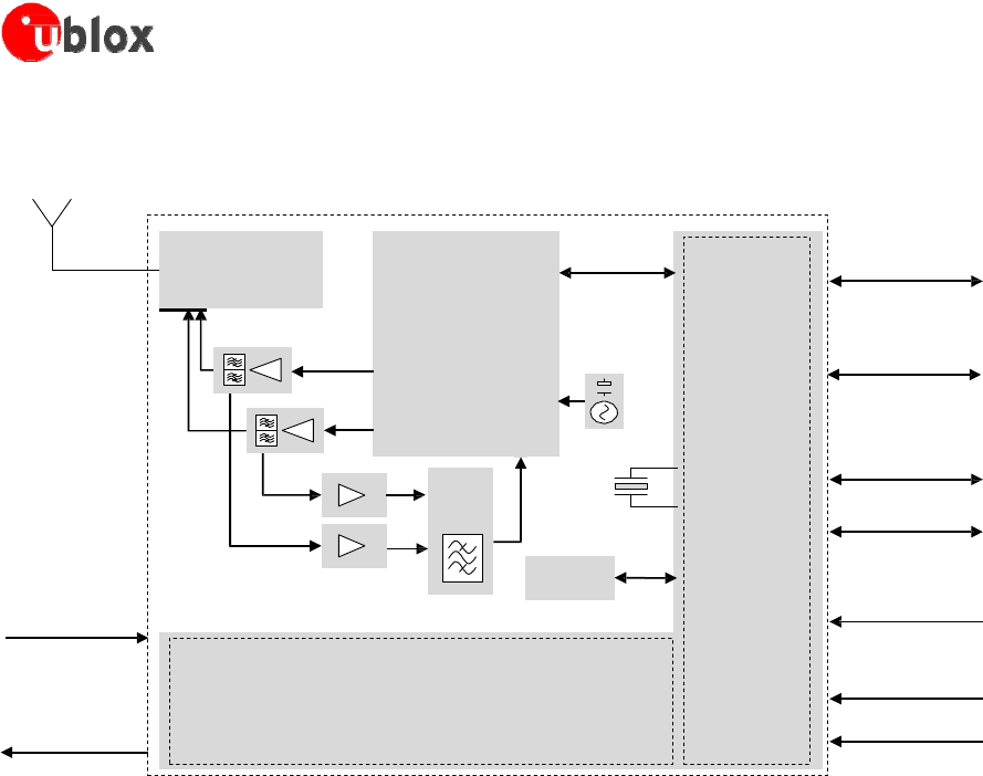
Figure 1: Block
diagram
1.2.1
Functional
bloc
k
s
LISA-C200
&
F
W75-
C
200
modul
e
s
c
on
s
i
s
t
of the following internal functional
bl
ock
s
:
RF
front-end,
RF
t
r
ansce
i
ve
r,
Baseband
s
e
ction
and
P
ow
e
r
Management
Unit.
RF
F
ron
t
-
End
The
Antenna connector
is
directly connected to the
Diplexer
which
s
e
pa
r
a
t
e
s
the 800 and 1900 MHZ bands.
Each
800 & 1900 MHz
RF
chain are connected to their
respective
t
r
ansce
i
ve
r
pa
t
h
s
via
duplexers as
s
ho
w
n
in
prior block diagram.
Each duplexer
prov
i
de
s
the filtering and
Rx/Tx
path
s
e
pa
r
a
t
ion
before
connecting
to the
LNA
and
RF PA
de
vi
ce
s
.
A
s
e
pa
r
a
t
e
shield
compartment
houses
the 800
MHZ
and 1900
MHZ RF
power
a
mpli
f
i
e
r
s
.
This
compartment
provid
e
s
high
Tx signal
i
s
ol
a
t
ion,
preventing de-sensing
of the
Rx
frontend circuitry.
RF
Tr
ans
cei
ver
The
t
r
ansce
i
ve
r
i
ncl
u
de
s
the following
key
components:
Dual-band
800 & 1900 MHz CDMA
t
r
ansce
i
ve
r,
excluding
the
RF P
ow
e
r
Ampli
f
i
e
r
s
,
duplexers
and diplexer.
19.2 MHz
Crystal O
s
ci
ll
a
t
or
While operating, the
RF
t
r
ansce
i
ve
r
performs direct
up-
conve
r
s
ion
and
d
ow
n-
conv
e
r
s
ion
of the
baseband
I
/Q
signals,
with the
RF
voltage controlled gain amplifier being
used
to
s
e
t
the uplink
TX
power.
In
the
do
w
nlink
path, the internal
LNA enhances
the
RX
s
e
n
s
i
t
i
v
i
t
y.
An internal automatic gain control amplifier
op
t
imi
ze
s
the
signal levels
before
delivering
to the
analog I/Q
to
baseband
for further digital
proce
ss
ing.

LIS
A
-C200
&
F
W75-
C
200
-
S
yste
m
I
nte
gra
t
ion
Manual
CDMA-2X-11004-3
P
r
e
limin
a
r
y
System de
s
c
r
ipt
ion
Page
8 of 43
In
all the
mo
de
s
,
Tx
&
Rx RF synthesizers
are an on-chip voltage controlled
o
s
ci
ll
a
t
or
are used to generate the
local
os
ci
ll
a
t
or
s
ig
na
l.
The
f
r
e
qu
e
ncy
r
e
f
e
r
e
nce
to
RF synthesizers
are provided by a free running 19.2 MHz XO.
The Rx
path
locks
and
t
r
a
ck
s
to the
base
s
t
a
t
ion
carrier.
An
learning
algorithm
is implemented
to
capture
the
temperature
cha
r
a
ct
e
ri
s
t
i
c
of the xtal, comparing the XO and
carrier
f
r
e
qu
e
nci
e
s
,
while
me
a
s
uring
the
t
he
rmi
s
t
or
in
close
proximity to the
crystal
oscillator. A lookup table
is saved
over temperature and time.
The
known frequency difference of the
free running
crystal
osc
ill
a
t
or
is corrected
in the
baseband processor enabling
quick
ac
qui
s
i
t
ion.
Baseband section
and power management
unit
Another
s
hi
e
lding
s
e
ction
i
ncl
u
de
s
all the digital circuitry and the power
supplies, basically
the
f
oll
ow
ing
functional
bl
ock
s
:
Wireless baseband processor,
a
mixed signal ASIC
which
i
nt
e
gra
t
e
s
:
Micropr
oce
ss
or
for controller
f
unction
s
,
CDMA upper
layer
s
oft
w
a
r
e
ARM9 coprocessor
and HW
acce
l
e
r
a
t
or
for CDMA
Layer
1 control
s
oft
w
a
r
e
and
rou
t
i
ne
s
D
e
di
ca
t
e
d
HW for
pe
riph
e
r
a
l
s
control,
as UART, USB,
etc
Memory
sys
t
e
m
in a Multi-Chip
P
a
ck
a
ge
(MC
P
)
integrating two
d
e
vi
ce
s
:
N
OR
f
l
a
s
h
non-volatile
memory
DDR
S
RA
M
vol
a
t
il
e
memory
P
ow
e
r
Management
Unit
(PMU), used
to
derive
all the
system
s
uppl
y
vol
t
a
ge
s
from the module
s
uppl
y
VCC
1.3
Pin
description
Table
2
pr
ovi
de
s
a
s
um
ma
r
y
of the module pin
names
and
d
e
s
cr
i
ptio
n
s
.
For
the
exact
s
pe
ci
f
i
ca
t
ion
including pin numbering and additional information
see
the
LISA-C200
Data
S
he
e
t
[1] or the
FW75-C200
D
a
t
a
S
he
e
t
[2].
Name
M
odule
P
ow
er
domain
I
/O
De
sc
ri
pt
ion
Rem
ark
s
VCC All VCC -
Module supply Module
supply inpu
t
V_
I
N
T
F
W75-
C
200 -
O
Digital
I/O Inte
r
f
a
c
e
s
supply
V_INT
= 2.85V
(
t
y
p
ic
al)
generated
by the module
output
when it is
s
wit
c
h
e
d-on and the
RESET_N
(
e
x
t
e
rn
a
l
r
e
se
t
input pin) is not forced to the low le
v
el.
V_INT
= 1.8V
(
t
y
p
ic
a
l
)
generated by the module
LISA-C200
-
O
Digital
I/O Inte
r
f
a
c
e
s
supply
output
when it is
s
wit
c
h
e
d-on and the
RESET_N
(
e
x
t
e
rn
a
l
r
e
se
t
input pin) is not forced to the low level.
P
W
R
_
ON
All
P
O
S
I
P
ower-on inpu
t
PWR_ON
pin
has
Internal pull-up resistor.
G
P
IO
1..10
LISA-C200
GD
I
I/O
G
P
IO
G
P
IO
6..10
Reserved.
R
ESE
T
_
N
LISA-C200
E
R
S
I
E
x
t
e
rn
a
l r
e
s
e
t
inpu
t
RESET_N
pin
has
Internal pull-up resistor.
H
W
_
S
HU
T
DO
W
N
F
W75-
C
200
E
R
S
I
E
x
t
e
rn
a
l
S
hu
t
do
wn
inpu
t
H
W
_
S
HU
T
DO
W
N
pin
has
Internal pull-up resistor.
A
N
T
All A
N
T
- I/O
RF
antenna
S
T
A
T
U
S
F
W75-
C
200
GD
I
O
LED
Indicator
Ind
ic
a
t
e
d by buffered
E
x
t
e
rn
a
l
LED
:
Off – Not
P
ower
e
d
On –
P
o
w
e
r
e
d,
a
sso
c
ia
t
e
d, and authenticated bu
t
not transmitting or receiving.
S
low
Blink
but not
a
sso
c
ia
t
e
d or authenticated;
se
a
r
c
hing.
Intermittent
Blink
- activity proportional
t
o
transmitting/receiving speed.
F
or voice
applications, turning off and on the
intermittent blink
based
on the ring pulse
cycle
can indicate a ring event.

LIS
A
-C200
&
F
W75-
C
200
-
S
yste
m
I
nte
gra
t
ion
Manual
CDMA-2X-11004-3
P
r
e
limin
a
r
y
System de
s
c
r
ipt
ion
Page
9 of 43
Name Module
P
ow
er
domain
I/O
Description
Rem
ark
s
RI
C
T
S
R
T
S
LISA-C200
F
W75-
C
200
LISA-C200
F
W75-
C
200
LISA-C200
F
W75-
C
200
GDI
O
UART
ring indicator Circuit 125
(RI)
in
ITU-T
V.24.
Value
at internal r
e
se
t
:
T
/
P
U
.
Use
to wake up host
processor. The
output signal
is
a
c
t
iv
e
low
.
Internal
a
c
t
iv
e
pull-up to 1.8 V.
Internal
a
c
t
iv
e
pull-up to 2.85 V
GDI
O
UART clear
to send Circuit 106
(CTS)
in
ITU-T
V.24.
Internal
a
c
t
iv
e
pull-up to 1.8 V.
Internal
a
c
t
iv
e
pull-up to 2.85 V.
GDI
I
UART ready
to
send
Circuit 105
(RTS)
in
ITU-T
V.24.
Internal
passive
pull-up to 1.8 V.
Internal passive
pull-up to 2.85 V.
GDI
O
UART received
data Circuit 104
(RxD)
in
ITU-T
V.24.
RXD
LISA-C200
F
W75-
C
200
TXD
LISA-C200
F
W75-
C
200
Internal
a
c
t
iv
e
pull-up to 1.8 V.
Internal
a
c
t
iv
e
pull-up to 2.85 V.
GDI
I
UART
t
r
a
n
s
mi
tt
e
d data Circuit 103
(TxD)
in
ITU-T
V.24.
Internal
passive
pull-up to 1.8 V.
Internal passive
pull-up to 2.85 V.
VUSB_DET
All
USB
I
USB
detect input Input for
VBUS (5
V
t
y
p
ic
a
l
)
USB supply
s
e
n
se
.
USB_D-
All
USB
I/O
USB
D
a
t
a
Line
D- 90 nominal differential impedance.
P
ull-up or pull-down
resistors
and external
se
ri
e
s
resistors as
required by the
USB
2.0 high-speed
specification [9] are part of the
USB
pad driver
and
need
not be
provided
externally.
USB_D+
All
USB
I/O
USB
D
a
t
a
Line
D+ 90 nominal differential impedance.
P
ull-up or pull-down
resistors
and external
se
ri
e
s
resistors as
required by the
USB
2.0 high-speed
specification [9] are part of the
USB
pad driver
and
need
not be
provided
externally.
MIC_N
LISA-C200
AUDIO
I
Differential
analog
audio
input
(
n
e
g
a
t
iv
e
)
M
IC
_
P
LISA-C200
AUDIO
I
Differential
analog
audio
input
(
po
sit
iv
e
)
SPK_P
LISA-C200
AUDIO O Differential
analog
audio
output
(
po
sit
iv
e
)
SPK_N
LISA-C200
AUDIO O Differential
analog
audio
output
(
n
e
g
a
t
i
v
e
)
Differential
analog
microphone inpu
t
.
Internal
DC blocking 0.1
µF
capacitor.
Differential
analog
microphone inpu
t
.
Internal
DC blocking 0.1
µF
capacitor.
Differential analog audio output shared for all
path mod
e
s
: earpiece, headset and loud
sp
ea
k
e
r
mode.
Differential analog audio output shared for all
path mod
e
s
: earpiece, headset and loud
sp
ea
k
e
r
mode.
PCM_SYNC
LISA-C200 GDI
O Digital
Sync
Digital Audio
Sync
pulse.
P
C
M
_
DO
LISA-C200 GDI
O Data Output Digital Audio
O
u
t
pu
t
.
PCM_CLK
LISA-C200 GDI
O Clock Output Digital Audio Clock
O
u
t
pu
t
.
P
C
M
_
D
I
LISA-C200 GDI
I
Data Input Digital Audio Input.
SCL
LISA-C200
DDC O
I
2
C bus
clock line
F
ix
e
d open drain. No internal pull-up.
Value
at internal r
e
s
e
t
:
T
.
SDA LISA-C200
DDC I/O I2C
bus
data line
F
ix
e
d open drain. No internal pull-up.
Va
lu
e
a
t
int
e
rn
a
l r
e
s
e
t
:
T
.
S
I
M
_
C
L
K
All
S
I
M
O
S
I
M
c
loc
k
Va
lu
e
a
t
int
e
rn
a
l r
e
s
e
t
:
L
.
SIM_IO
All
SIM
I/O
SIM
data
Internal
4.7 k pull-up
resistor
to
V
S
I
M
.
Value
at internal r
e
s
e
t
:
L
/
P
D
.
S
I
M
_
R
S
T
All
SIM
O
SIM
reset
Value
at internal r
e
s
e
t
:
L
.
VSIM
ALL - O
SIM supply
output 1.80 V typical or 2.90 V typical generated by the
module
according
to the
SIM card
type.
S
I
M
_
GND
F
W75-
C
200
SIM
O
SIM
G
R
OUND
RSVD
All
RSVD
-
RESERVED
pin
Unless
otherwise specified,
leave
unconnected.
GND All GND - Ground All
GND pads
must be
connected
to ground.
Table
2: Pin description
s
ummary
LIS
A
-C200
&
F
W75-
C
200
-
S
yste
m
I
nte
gra
t
ion
Manual
CDMA-2X-11004-3
P
r
e
limin
a
r
y
System de
s
c
r
ipt
ion
Page
10 of 43
1.4 Power managemen
t
1.4.1
Power supply circuit overvie
w
LISA-C200
&
F
W75-
C
200
modul
e
s
feature a power
management concept
optimized for the
mo
s
t
efficient
use
of
s
uppli
e
d
power.
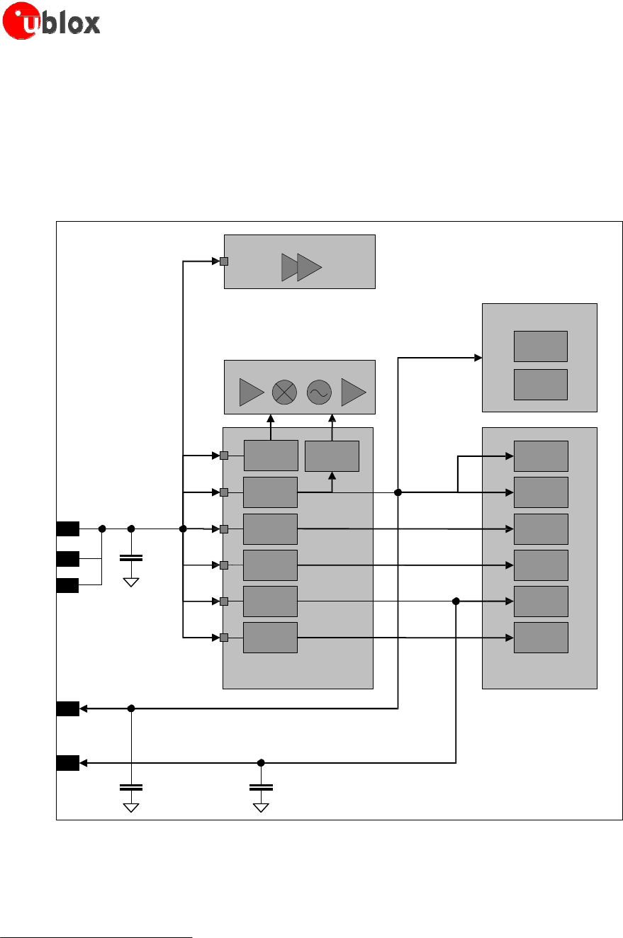
This is achieved
by
hardware
de
s
ign
utilizing a power efficient circuit topology
(Figure 2),
and by
power
management
software controlling the
mo
du
l
e
’s
power
saving
mode.
2 x 3G Power Amplifier(s)
u-blox C200
Mem
ory
NOR
F
l
a
s
h
RF
Tr
an
sc
eiver
DDR
SR
AM
L
in
ear
L
DO
L
in
ea
r
L
DO
EB
U
V
CC
V
CC
VCC
42
µ
F
Sw
itching
Step
-
Do
w
n
S
w
itching
Step
-
Do
w
n
L
in
ear
L
DO
L
in
ear
L
DO
I
/
O
CO
R
E
An
al
og
SI
M
L
in
ear
L
DO
R
TC
Power Management
Uni
t
Baseband
Processor
V_INT
V
S
I
M
4.7
µF
2.2
µ
F
Figure 2: Power
management
s
impli
fi
ed
block
diagram
Pins
with
s
uppl
y
function
are
reported in
Table
3.
LISA-C200
&
FW75-C200
modul
e
s
must be
s
uppli
e
d
via the VCC
pin
s
.
There is
only one main power
s
uppl
y
input,
available
on the three1 or five2
VCC
pin
s
that
mu
s
t
be all
connected
to the
external
power
s
uppl
y
1
LISA-C200
.

LIS
A
-C200
&
F
W75-
C
200
-
S
yste
m
I
nte
gra
t
ion
Manual
CDMA-2X-11004-3
P
r
e
limin
a
r
y
System de
s
c
r
ipt
ion
Page
11 of 43
The
VCC
pins are directly
connected
to the
RF
power
a
mpli
f
i
e
r
s
and to the integrated
P
ow
e
r
Management Unit
(PMU)
within the module: all
s
uppl
y
vo
l
t
a
ge
s
needed by the module are generated from the VCC
s
uppl
y
by
integrated
vol
t
a
ge
regulators.
When a 1.8 V or a 3 V
S
I
M
card type
is connected,
LISA-C200
&
FW75-C200
modul
e
s
automatically
s
uppl
y
the
S
I
M
card via the VSIM pin. Activation and
deactivation
of the
S
I
M
interface with automatic voltage
s
w
i
t
ch
f
rom
1.8 to 3 V
is implemented,
in
accordance
to the
ISO-IEC
7816-3
s
pe
c
i
f
i
ca
t
ion
s
.
The
2.8 voltage domain
used
internally
also available
on the V_INT pin, to allow more
economical
and efficient
integration of the
LISA-C200
&
F
W75-
C
200
modul
e
s
in the final application.
The
integrated
P
ow
e
r
Management Unit
also
provi
de
s
the control
s
t
a
t
e
machine
for
system
s
t
a
r
t
up and
s
yste
m
s
hu
t
down control.
1.4.2 Module
supply (VCC)
LISA-C200
&
F
W75-
C
200
modul
e
s
must be
s
uppli
e
d
through the
VCC
pin
s
by a DC power
s
uppl
y.
Vol
t
a
ge
s
mu
s
t
be
s
t
a
bl
e
:
during operation, the current drawn from
VCC
can vary
by
some
orde
r
s
of magnitude.
Name De
sc
ri
pt
ion
Rem
ark
s
VCC Module power
supply inpu
t
VCC
pins
are
internally connected,
but all the
available p
a
d
s
or
pins
must be
connected
to the
e
x
t
e
rn
a
l
supply
in order
t
o
minimize the power
loss
due to
series
resistance.
Clean
and
stable supply is
required: low ripple and
low
voltage drop must be guaranteed.
Voltage
provided
must
always
be
above
the minimum limit o
f
the operating range.
GND Ground GND
pins
are
internally connected
but a good
(
low
impedance)
e
x
t
e
rn
a
l ground
can
improve
RF
performance:
all
available pads
or
pins
must be
connected
to ground.
Table
3:
Module
supply
pins
Higher ESD
protection
level can
be
required
if
VCC
is externally accessible
on the
application
board.
Higher
protection
level can
be
achieved
by mounting an
ESD
protection
(e.g. EPCOS
C
A05
P
4S
14
T
H
S
G
va
ri
s
t
or
array)
on the line
connected
to
t
hi
s
pin.
The
vol
t
a
ge
provided
to the
VCC
pins
mu
s
t
be within the normal operating
range
limi
t
s
as
s
pe
c
i
f
i
e
d
in
the
LISA-C200
D
a
t
a
S
he
e
t
[1] or
FW75-C200
D
a
t
a
S
he
e
t
[2].
Complete
functionality of the module
is
only
guaranteed
within the
s
pe
ci
f
i
e
d
minimum and
maximum
VCC
vo
l
t
a
ge
operating range.
Ensure
that the input voltage at the
VCC
pins never drops below the minimum limit of the operating
r
a
ng
e
when the module
is
s
w
i
t
che
d
on.
Operation above the operating range maximum limit is not recommended and
ex
t
ended
expo
su
re
beyond it may affect
device
reliab
ilit
y.
Stress
beyond the
VCC
absolute maximum
ra
t
ing
s
can cause
permanent damage to the
module:
if
necessary,
voltage
spikes
beyond
VCC
absolute maximum
ra
t
ing
s
mu
s
t
be
restricted
to values
within the
specified
limits by
using
appropriate protection.
When
de
s
igning
the power
s
uppl
y
for the application, pay
s
pe
ci
f
i
c
attention to power
losses
and
t
r
ans
i
e
nts.
The
DC power
s
uppl
y
must be able to provide a voltage profile to the VCC
pin
s
with the
following
cha
r
a
ct
e
ri
s
t
i
cs:
V
ol
t
a
ge
drop during
t
r
ans
mi
ss
ion
mu
s
t
be lower than 250 mV
2
F
W75-
C
200.
LIS
A
-C200
&
F
W75-
C
200
-
S
yste
m
I
nte
gra
t
ion
Manual
CDMA-2X-11004-3
P
r
e
limin
a
r
y
System de
s
c
r
ipt
ion
Page
12 of 43
Any degradation in power
s
uppl
y
performance
(due to
losses, noise
or
t
r
ans
i
e
nts)
will directly affect the
RF
performance of the module
since
the
single
external DC power
source
indirectly
supplies
all the
digital and
analog
inter
f
ace
s
,
and
also directly supplies
the
RF
power amplifier
(P
A
).
1.4.2.1
VCC
application
ci
r
cu
it
s
LISA-C200
&
FW75-C200
modul
e
s
must be
s
uppli
e
d
through the
VCC
pins by one (and only
one)
proper DC
power
s
uppl
y
that must be one of the
f
oll
ow
ing:
S
w
i
t
chi
ng
regulator
Low Drop-Out
(LDO) linear
regulator
Rechargeable Li-Ion
battery
P
ri
ma
r
y
(disposable)
b
a
tt
e
r
y
Main
S
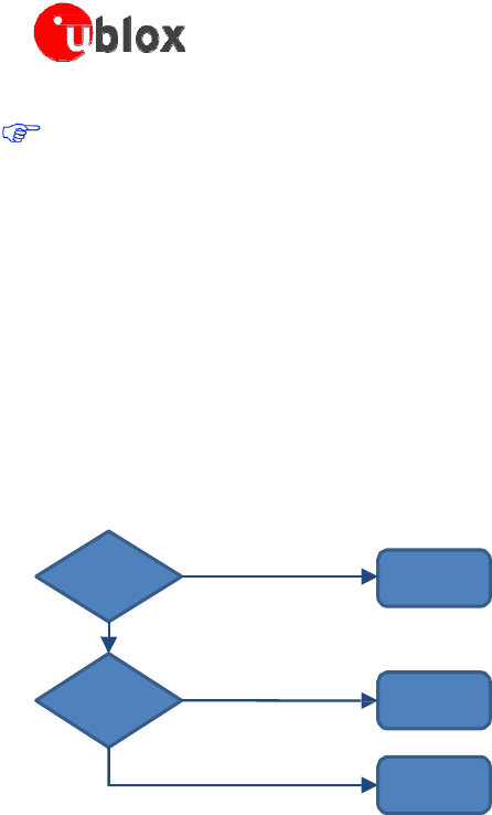
upply
Available?
No,
portable
device
B
a
tt
e
ry
Li-Ion
3.7
V
Yes, always
available
Main
S
upply
V
olta
ge
>5
V
?
No,
less
than 5 V
Yes, greater
than 5 V
Linear LDO
Re
gula
tor
S
witching
S
tep-Down
Re
gula
tor
Figure 3: VCC supply concept
s
ele
c
ti
on
The
s
w
i
t
chi
ng
s
t
e
p-do
w
n
regulator
is
the typical
choice
when the
available
primary
s
uppl
y
source has
a nominal
voltage much higher (e.g. greater than 5
V)
than the
LISA-C200
& FW75-C200
modul
e
s
operating
s
uppl
y
voltage.
The
use of
s
w
i
t
ch
ing
s
t
e
p-do
w
n
provi
de
s
the
be
s
t
power efficiency for the overall application and
minimi
ze
s
current drawn from the main
s
uppl
y
source.
The
use of an
LDO
linear regulator
becomes convenient
for a primary
s
uppl
y
with a
r
e
l
a
t
i
ve
l
y
low voltage (e.g.
less
than 5
V). In
t
hi
s
case
the typical 90% efficiency of the
s
w
i
t
chi
ng
regulator will
dimini
s
h
the benefit
of
voltage
s
t
e
p-do
w
n
and no true
advantage
will be gained in input current
savings.
On the opposite
side,
linear
regulators are not
recommended
for high voltage
s
t
e
p-do
w
n
as
they will
di
ss
i
pa
t
e
a
considerable
amount
o
f
energy
in thermal power.
I
f
LISA-C200
&
FW75-C200
modul
e
s
are
deployed
in a mobile unit where no
permanent primary
s
uppl
y
source
i
s
available,
then a battery will be required to provide VCC. A
s
t
a
nd
a
rd
3-cell
Li
t
hium-
I
on
battery pack directly
connected to VCC
is
the usual choice for battery-powered
devices.
During charging,
ba
tt
e
ri
e
s
with Ni-MH
che
mi
s
t
r
y
t
yp
i
ca
ll
y
reach
a
maximum
vol
t
a
ge
that
is above
the
maximum
rating for
VCC
,
and
s
hould
therefore be
avoided.
The use
of
primary
(not
rechargeable)
battery
is
uncommon,
since
the most
cells available
are
s
e
ldom
capable
of
delivering
the
peak
current due to high internal
r
e
s
i
s
t
a
nce
.
Keep
in mind that the
use
of
ba
tt
e
ri
e
s
requires
the implementation of a
s
ui
t
a
bl
e
charger
circuit (not included in
LISA-C200
&
F
W75-
C
200
modul
e
s
).
The charger
circuit
s
hould
be
de
s
ign
e
d
in order to prevent
ove
r-
vol
t
a
ge
on
VCC
beyond
the upper limit of the
absolute maximum
rating.
The
following
sections
highlight
some
de
s
ign
aspects
for
each
of the
supplies
li
s
t
e
d
above.
LIS
A
-C200
&
F
W75-
C
200
-
S
yste
m
I
nte
gra
t
ion
Manual
CDMA-2X-11004-3
P
r
e
limin
a
r
y
System de
s
c
r
ipt
ion
Page
13 of 43
Switching
regula
t
or
The
cha
r
a
ct
e
ri
s
t
i
cs
of the
s
w
i
t
chi
ng
regulator
connected
to
VCC
pin
s
s
hould
meet the following requirements:
Power
c
apabili
t
y
:
the
s
w
i
t
chi
ng
regulator with
i
t
s
output circuit
mu
s
t
be
capable
of providing a voltage
value
to the
VCC
pins within the
s
pe
c
i
f
i
e
d
operating range and
mu
s
t
be
capable
of delivering greater than
1.2
Amp
s
for
sa
f
e
de
s
ign
margin
L
o
w
output ripple: the
s
w
i
t
chi
ng
regulator together with
i
t
s
output circuit
mu
s
t
be
capable
of providing a
clean (low noise)
VCC
v
ol
t
a
g
e
profile
High switching
frequency:
for
be
s
t
performance
and for
smaller
a
ppli
ca
t
io
ns
select
a
s
w
i
t
chi
ng
frequency
600 kHz
(since L-C
output filter
is
typically
smaller
for high
s
w
i
t
ch
ing
f
r
e
qu
e
ncy).
The
use of a
s
w
i
t
ch
ing
regulator with a
variable
s
w
i
t
chi
ng
frequency or with a
s
w
i
t
ch
ing
frequency lower than 600 kHz
mu
s
t
be
ca
r
e
f
ull
y
eva
l
ua
t
e
d
since
t
hi
s
can produce
noise
in the
VCC
voltage profile. An additional
L-C
l
ow
-
pa
ss
f
il
t
e
r
between the
s
w
i
t
chi
ng
regulator output to
VCC
s
uppl
y
pin
s
can mitigate the ripple on
VCC
,
but
adds
extra
vol
t
a
ge
drop due to
re
s
i
s
t
i
ve
losses
on
series
inductors
PWM mode operation:
select
pre
f
e
r
a
bl
y
r
e
gul
a
t
ors
with
Pulse
Width Modulation
(PWM)
mode. While in
active
mode
Pulse Frequency
Modulation
(PFM)
mode and
P
FM
/P
W
M
mode
t
r
ans
i
t
ion
s
mu
s
t
be
avoided
t
o
reduce
the
noise
on the
VCC
voltage profile.
S
w
i
t
ch
ing
r
e
gul
a
t
ors
able to
s
w
i
t
ch
between low ripple
P
W
M
mode and high efficiency burst or
PFM
mode can be
used,
provided the mode transition from idle mode
(current
consumption
a
ppro
xi
ma
t
e
l
y
2
mA)
to
active
mode (current
consumption
a
p
proxim
a
t
e
l
y
100 mA):
i
t
is permissible
to use a regulator that
s
w
i
t
che
s
from the
P
W
M
mode to the
bur
s
t
or
PFM
mode at an
appropriate
current
t
hre
s
hold
(e.g.
60
mA
)
Output voltage
slope
:
( not
necessary
for CDMA
s
o
lution
,
ok to
del
et
e-
R
J
C
)
the
use
of the
s
oft
s
t
a
r
t
function provided by
some
voltage regulator
mu
s
t
be
ca
r
e
f
ull
y
eva
l
ua
t
e
d,
since
the voltage at the
VCC
pins
mu
s
t
ramp from 2.5 V to 3.2 V within 1
ms
to allow a proper
s
w
i
t
ch
-on
of the module
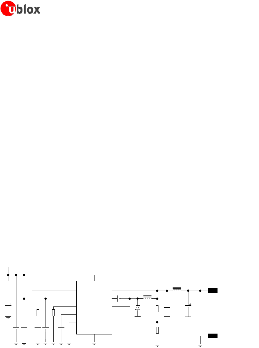
Figure
4 and the
com
po
ne
n
t
s
li
s
t
e
d
in
Table
4
s
h
ow
an
example
of a high reliability power
s
uppl
y
circuit, where
the module
VCC
is
s
uppli
e
d
by a
s
t
e
p-do
w
n
s
w
i
t
ch
ing
regulator
capable
of
delivering
2.5 A current
pulses
w
i
t
h
low output ripple and with fixed
s
w
i
t
ch
ing
f
r
e
qu
e
ncy
in
P
W
M
mode operation
gre
a
t
e
r
than 1 MHz.
The use
of a
s
w
i
t
chi
ng
regulator
is
s
ugg
e
s
t
e
d
when the difference from the
available
s
uppl
y
rail to the VCC value
is
high:
s
w
i
t
chi
ng
r
e
gul
a
t
ors
provide good
e
ff
i
ci
e
ncy
transforming a 12 V
s
uppl
y
to the typical 3.8 V value of the VCC
s
uppl
y.
12V
u-blox C200
R1
5
9
10
C1
R
UN
VC
RT
4
V
I
N
BD
1
BOOST
2
SW
3
C7
L1
L2
C8 C9
VCC
C2 C3
R2 R3
C4 C5 C6
7 PG
6 SYNC
U1
GND
11
FB
8
D1
R4
R5
GND
Figure 4: Suggested schematic design
for the
VCC
voltage
supply appli
c
a
t
ion
circuit
using a
s
te
p-
dow
n regula
tor
LIS
A
-C200
&
F
W75-
C
200
-
S
yste
m
I
nte
gra
t
ion
Manual
CDMA-2X-11004-3
P
r
e
limin
a
r
y
System de
s
c
r
ipt
ion
Page
14 of 43
Reference De
sc
ri
pt
ion
Part
Number –
M
an
ufa
c
ture
r
C1 47
µF
Capacitor
Aluminum 0810 50 V
M
A
L
215371479
E
3 – Vishay
C2 10
µF
Capacitor Ceramic X7R
5750 15% 50 V
C5750X7R1H106MB
–
T
DK
C3 10
nF
Capacitor Ceramic X7R
0402 10% 16 V
G
R
M
155
R
71
C
103
KA
01 –
M
ur
a
t
a
C4 680
pF
Capacitor Ceramic X7R
0402 10% 16 V
G
R
M
155
R
71
H
681
KA
01 –
M
ur
a
t
a
C5 22
pF
Capacitor Ceramic COG
0402 5% 25 V
G
R
M
1555
C
1
H
220
J
Z
01 –
M
ur
a
t
a
C6 10
nF
Capacitor Ceramic X7R
0402 10% 16 V
G
R
M
155
R
71
C
103
KA
01 –
M
ur
a
t
a
C7 470
nF
Capacitor Ceramic X7R
0603 10% 25 V
G
R
M
188
R
71
E
474
KA
12 –
M
ur
a
t
a
C8 22
µF
Capacitor Ceramic X5R
1210 10% 25 V
G
R
M
32
E
R
61
E
226
KE
15 –
M
ur
a
t
a
C37 330
µF
Capacitor Tantalum
D_SIZE
6.3 V 45 m
T
520
D
337
M
006A
T
E
045 -
K
E
M
E
T
D1
S
c
ho
tt
k
y
Diode
40 V 3 A
M
B
R
A340
T
3
G
-
ON
S
e
mi
c
ondu
c
t
or
L1 10 µH Inductor 744066100 30% 3.6 A 744066100 - Wurth
E
l
e
c
t
ron
ic
s
L2 1 µH Inductor 7445601 20% 8.6 A 7445601 - Wurth
E
l
e
c
t
ron
ic
s
R1 470 k
Resistor
0402 5% 0.1 W 2322-705-87474-
L
- Yageo
R2 15 k
Resistor
0402 5% 0.1 W 2322-705-87153-
L
- Yageo
R3 22 k
Resistor
0402 5% 0.1 W 2322-705-87223-
L
- Yageo
R4 390 k
Resistor
0402 1% 0.063 W
R
C
0402
F
R
-07390
KL
- Yageo
R5 100 k
Resistor
0402 5% 0.1 W 2322-705-70104-
L
- Yageo
U1
S
t
e
p Down
R
e
gul
a
t
or
M
S
O
P
10 3.5 A 2.4 MHz
LT3972IMSE#PBF
-
Linear
T
e
c
hnolog
y
Table
4: Suggested
c
omp
onents
for the
VCC
voltage
supply appli
c
a
ti
on
circuit using
a
s
te
p-do
w
n regula
tor
L
o
w
Drop-Out
(LDO)
linear
regul
at
or
The
cha
r
a
ct
e
ri
s
t
i
cs
of the LDO linear regulator connected to the VCC
pin
s
s
hould
meet the
f
oll
ow
ing
requirements:
Power
c
apabili
t
ies
:
the
LDO
linear regulator with
i
t
s
output circuit
mu
s
t
be
capable
of providing a proper
vol
t
a
ge
value
to the
VCC
pin
s
and of
delivering
1.2 A
Power
dissipation
:
the power handling
ca
pa
bili
t
y
of the
LDO
linear regulator must be
checked
to limit
i
t
s
junction
temperature
to the
maximum
rated operating
range (i.e. check
the
vol
t
a
ge
drop from the
max
inp
ut
vol
t
a
ge
to the min output
vo
l
t
a
ge
to
eva
l
ua
t
e
the power
di
ss
i
pa
t
ion
of the regulator)
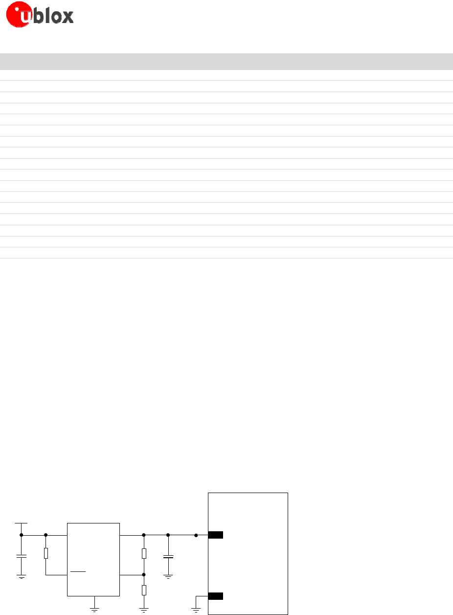
Figure
5 and the components
li
s
t
e
d
in
Table
5
s
ho
w
an example of a power
s
uppl
y
circuit, where the VCC
module
s
uppl
y
is
provided by an
LDO
linear regulator capable of delivering 1.2
Amp
s
,
with proper power
handling
ca
pa
bili
t
y.
The use
of a linear regulator
is
s
ugg
e
s
t
e
d
when the
difference
from the
available
s
uppl
y
rail
and the
VCC value is
low: linear
r
e
gul
a
t
ors
provide high
e
ff
i
ci
e
ncy
when transforming a 5 V
s
uppl
y
to the 3.6 V
t
ypi
ca
l
value
of the
VCC
s
uppl
y.
u-blox
C
200
5V
2 IN
OUT
4
VCC
C1 R1
1
S
HDN
U1
GND
3
ADJ
5
R2 C2
R3
GND
Figure 5: Suggested schematic design
for the
VCC
voltage
supply appli
c
a
t
ion
circuit
using an
LDO
linear regula
to
r

CDMA-2X-11004-3
P
r
e
limin
a
r
y
System de
s
c
r
ipt
ion
Page
15 of 43
LI
S
A-
C
200
&
F
W75-
C
200
-
S
yste
m
I
nte
gra
t
ion
Manual
Reference De
sc
ri
pt
ion
Part
Number -
M
anufacturer
C1 10
µF
Capacitor Ceramic X5R
0603 20% 6.3 V
G
R
M
188
R
60
J
106
M
E
47 -
M
ur
a
t
a
C2 10
µF
Capacitor Ceramic X5R
0603 20% 6.3 V
G
R
M
188
R
60
J
106
M
E
47 -
M
ur
a
t
a
R1 47 k
Resistor
0402 5% 0.1 W
R
C
0402
J
R
-0747
KL
-
Yageo
P
h
yc
omp
R2 4.7 k
Resistor
0402 5% 0.1 W
R
C
0402
J
R
-074
K7L
-
Yageo
P
h
yc
omp
R3 2.2 k
Resistor
0402 5% 0.1 W
R
C
0402
J
R
-072
K2L
-
Yageo
P
h
yc
omp
U1
LDO Linear
R
e
gul
a
t
or A
D
J
3.0 A
L
T
1764A
E
Q
#
P
B
F
-
Linear
T
e
c
hnolog
y
Table
5: Suggested
c
omp
onents
for
VCC
voltage
supply appli
c
a
ti
on
circuit using
an
LDO
linear regula
tor
Rechargeable Li-Ion
ba
tt
ery
Rechargeable Li-Ion
b
a
tt
e
ri
e
s
connected
to the
VCC
pins
s
hould
meet the following requirements:
Maximum pulse and DC
discharge
current: the
rechargeable Li-Ion
battery with
i
t
s
output circuit must be
capable
of
delivering
1.2 A to the
VCC
pins
and must be
capable
of
delivering
a DC current
gre
a
t
e
r
than the
module
maximum average
current
consumption
to
VCC
pin
s
.
The maximum pulse discharge
current and the
maximum DC
discharge
current are not
always
reported in battery data
s
he
e
t
s
,
but the maximum DC
discharge
current
is
t
yp
i
ca
ll
y
a
lmo
s
t
equal
to the battery
ca
pa
ci
t
y
in
Amp-hours divided
by 1 hour
DC
series resistance
:
the
rechargeable Li-Ion
battery with
i
t
s
output circuit
mu
s
t
be
capable
of avoiding a
VCC
v
ol
t
a
ge
drop
gre
a
t
e
r
than 250 mV during
peak currents (Max Tx
P
ow
e
r
).
Primary (disposable)
b
at
t
ery
The
cha
r
a
ct
e
ri
s
t
i
cs
of a primary
(non-rechargeable)
battery connected to VCC
pin
s
s
hould
meet the
f
oll
ow
ing
requirements:
Maximum pulse and DC
discharge
current: the
non-rechargeable
battery with
i
t
s
output circuit
mu
s
t
be
capable
of
delivering
1.2 A to the
VCC
pins
and must be
capable
of
delivering
a DC current
gre
a
t
e
r
than the
module
maximum average
current
consumption
at the
VCC
pin
s
.
The maximum pulse
and the
maximum
DC
discharge
current
is
not
always
reported in battery data
s
he
e
t
s
,
but the maximum DC
discharge
current
i
s
t
ypi
ca
ll
y
a
lmo
s
t
equal
to the battery
ca
pa
ci
t
y
in
Amp-hour
s
divided
by 1 hour
DC series
resistance
:
the
non-rechargeable
battery with
i
t
s
output circuit must be
capable
of avoiding a
VCC
v
ol
t
a
ge
drop
gre
a
t
e
r
than 250 mV during
peak currents (Max Tx
P
ow
e
r
).
Additional
r
eco
mmend
at
ion
s
for the
VCC supply
application
ci
r
cu
it
s
To
reduce voltage drops, use a low impedance power
source. The
r
e
s
i
s
t
a
nce
of the power
s
uppl
y
li
ne
s
(connected
to the
VCC
and GND pins of the
module)
on the application board and battery pack
s
hould
also
be
considered
and
minimized: cabling
and routing must be
as
s
hor
t
as possible
in order to
minimize
power
l
os
s
e
s
.
Three
3
or five4
pin
s
are
a
ll
oca
t
e
d
for
VCC
s
uppl
y
.
Another
seven
pins are
de
s
ig
na
t
e
d
for GND
connection.
Even
i
f
all the
VCC
pins
and all the GND
pins
are
internally connected
within the module, it
is recommended
to properly
connect
all of them to
s
uppl
y
the module in order to
minimize series
r
e
s
i
s
t
a
nce
l
os
s
e
s
.
The
placement ceramic capacitors on the VCC line on the main board close to the connector will benefit
operation.
To reduce
vol
t
a
ge
ripple and
noise, place
the following
near
the
VCC
pins:
100
nF
ca
pa
ci
t
or
(e.g
Murata
GRM155R61A104K)
to filter digital logic
noise
from
clocks
and data
s
o
urc
e
s
22
µF
ca
pa
c
i
t
or
(e.g.
Murata
GRM31
C
R
60
J
22
6K)
to
s
uppl
y
local
DC energy.
Figure
6
s
ho
w
s
the
complete
configuration but the mounting of
each single
component
depe
nd
s
on the
a
ppli
ca
t
ion
de
s
ign.
3
LISA-C200
.
4
F
W75.
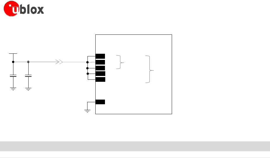
CDMA-2X-11004-3
P
r
e
limin
a
r
y
System de
s
c
r
ipt
ion
Page
16 of 43
LI
S
A-
C
200
&
F
W75-
C
200
-
S
yste
m
I
nte
gra
t
ion
Manual
u-blox
C2
00
3.6V
VCC
VCC
VCC
LISA-C200
+ VCC
F
W75
C1 C2 VCC
GND
Figure 6: Suggested schematic design
to
reduce
voltage ripple and
noise
and to avoid under
s
ho
ot/
overshoot on voltage drops
Reference De
sc
ri
pt
ion
Part
Number -
M
anufacturer
C1 22
µF
Capacitor
Ceramic 6.3 V 45
G
R
M
31
C
R
60
J
226
K
-
M
ur
a
t
a
C2 100
nF
Capacitor Ceramic X7R
0402 10% 16 V
G
R
M
155
R
61A104
KA
01 -
M
ur
a
t
a
Table
6: Suggested
c
omp
onents
to
reduce
voltage ripple and
noise
and to avoid under
s
h
oot/
overshoot on voltage drops
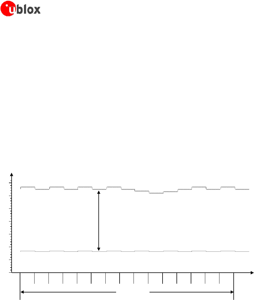
CDMA-2X-11004-3
P
r
e
limin
a
r
y
System de
s
c
r
ipt
ion
Page
17 of 43
LI
S
A-
C
200
&
F
W75-
C
200
-
S
yste
m
I
nte
gra
t
ion
Manual
1.4.3 Current
consumption
profi
le
s
During operation, the current drawn by the
LISA-C200
&
FW75-C200
modul
e
s
through the
VCC
pin
s
can vary
by
several
orde
r
s
of magnitude.
This ranges
from
c
on
t
inuou
s
high current drawn in CDMA
connected
mode, to the
low current
c
on
s
um
ptio
n
during in idle mode.
1.4.3.1 CDMA
connected
mode
During a CDMA connection, the module can transmit and
receive
continuou
s
l
y
due to the
Frequency
D
i
vi
s
ion
Duplex
(FDD)
mode of operation with the Code
Division
Multiple
Access (CDMA). The
current consumption
depe
nd
s
again on output
RF
power, which
is always
regulated by network
com
m
a
nd
s
.
These
power control
commands
are
logically divided
into a
s
l
ot
of 1.25
ms,
thus the rate of power
change can reach
a
maximum
rate
of 800
Hz. Since
t
r
ans
mi
ss
ion
and
reception are
continuou
s
l
y
enabled
due to
FDD
CDMA
implemented
in the 3G
that
di
ff
e
r
s
from the
TDMA
implemented in the 2G
case. In
the worst
scenario,
c
orr
e
s
ponding
to a
co
ntin
uou
s
t
r
ans
mi
ss
ion
and reception at maximum output power
(a
ppr
oxima
t
e
l
y
250 mW or 24
dBm),
the current
dra
w
n
by the module at the VCC pins
is
in the order of continuous 600-700 mA.
Even
at
l
ow
e
s
t
output
RF
power
(a
ppr
oxima
t
e
l
y
0.01 µW or -50
dBm),
the current
is
in the order of
less
than 100 mA due to module
ba
s
e
ba
nd
processing
and
transceiver
activity.
An example of current
con
s
um
ptio
n
profile of the data module in CDMA continuous
t
r
ans
mi
ss
ion
mode
i
s
s
ho
w
n
in
F
igur
e
7.
Curre nt
[mA]
700
610
mA
600
500
400
Depends on TX pow
er
300
200
100
<100
mA
Not actual data
f
or
illustration
0
1
slot
3G
frame
Time
[ms]
Figure 7: VCC
c
urren
t
c
ons
um
pti
on profile
versus
time during a CDMA
connection,
with
VCC=3.8
V
When a packet data connection
is
e
s
t
a
bli
s
he
d,
the actual current profile
depe
nd
s
on the amount of transmitted
pack
e
t
s
;
there might be
some
periods of inactivity between allocated
slots
where current
con
s
ump
t
ion
drop
s
about 100 mA.
Alternatively,
at higher data
r
a
t
e
s
the transmitted power
is
likely to
increase
due to the higher
quality
signal required
by the network to
cope
with
enhanced
data
s
pe
e
d.

CDMA-2X-11004-3
P
r
e
limin
a
r
y
System de
s
c
r
ipt
ion
Page
18 of 43
LI
S
A-
C
200
&
F
W75-
C
200
-
S
yste
m
I
nte
gra
t
ion
Manual
1.5
System
f
un
ct
ion
s
1.5.1 Module power on
The
module power on
sequence is
initiated in one of
t
he
s
e
ways:
Rising
edge on the
VCC
pin to a valid voltage for module
s
uppl
y
AND if the
PWR_ON
pin
is
permanently
l
ow
when
VCC is
applied
Falling edge
on the
PWR_ON
pin (pin
mu
s
t
be held low for >150
ms
ec
)
Name De
sc
ri
pt
ion
Rem
ark
s
P
WR_
ON
P
ower on inpu
t
PWR_ON
pin
has
internal pull up
resistor.
R
e
c
om
me
nd
e
d
t
o
use
open collector or drain configuration to pull do
wn
.
Table
7: Power
on pin
The
PWR_ON
pin
ESD
s
ens
i
t
i
vi
t
y
rating
is
1 kV
(Human Body
Model
according
to
J
ES
D
22-A11
4F).
Higher
prot
e
ction
level could be required if the line
is externally accessible
on the application board. Higher
protection
level
can be
achieved
by mounting an
ESD
protection (e.g.
EPCOS
C
A05
P
4S
14
T
H
S
G
va
ri
s
t
or
array)
on the line
connected
to
thi
s
pin.
1.5.1.1
Rising
edge on
V
CC
\When a
s
uppl
y
is
connected to VCC pins, the module
s
uppl
y
supervision
circuit
c
on
t
rol
s
the
s
ub
s
e
qu
e
nt
activation
of the power up
s
t
a
t
e
machi
ne
s
:
the module
is
s
w
i
t
che
d
on when the
vol
t
a
ge
rises
up to the VCC
operating
range
minimum limit (3.4
V)
s
t
a
r
t
ing
from a
v
ol
t
a
ge
value
lower than 2.25 V
(See
LISA-C200
Data
S
he
e
t
[1] or the
F
W75-
C
200
Data
S
he
e
t
[2]), provided
that the
PWR_ON
pin
is permanently
low when VCC
is
applied.
1.5.1.2
Falling
edge on
PWR
_ON
The
module power on
sequence
s
t
a
r
t
s
when a falling
edge is
forced on the
PWR_ON
input pin. After
applying
a
falling edge, it
is
s
ug
ge
s
t
e
d
to hold a low
level
on the
PWR_ON
signal
for at
l
ea
s
t
300 ms to properly
s
w
i
t
ch
on
the module.
The electrical
cha
r
a
ct
e
ri
s
t
i
cs
of the
PWR_ON
input pin
are
different from the other digital
I/O
inter
f
ace
s
:
the high
and the low logic
levels have
different operating
ranges
and the pin
is
not-tolerant to
vol
t
a
ge
s
up to the battery
voltage.
The
detailed
electrical cha
r
a
ct
e
ri
s
t
i
cs
are
described
in the
LISA-C200
Data
S
he
e
t
[1] or the FW75-C200
D
a
t
a
S
he
e
t
[2].
Once
the module
has been
turned on,
PWR_ON
pin
has
no effect. On the other hand it
makes
no
sense
to keep
t
hi
s
pin low
once
the module
has been
turned on: if the pin
is
kept low it will draw
unnecessary
current.
Following are some
t
yp
i
ca
l
examples
of
application
ci
r
cu
i
t
s
to turn the module on
using
the
PWR_ON
input pin.
The
s
impl
e
s
t
way to turn on the module
is
to
use
a
pu
s
h
button that
s
h
ort
s
the
PWR_ON
pin to ground.
I
f
the
PWR_ON
input
is connected
to an
external device
(e.g. application
processor),
it
is
s
ug
ge
s
t
e
d
to
use
an
open drain output on the
external
device.
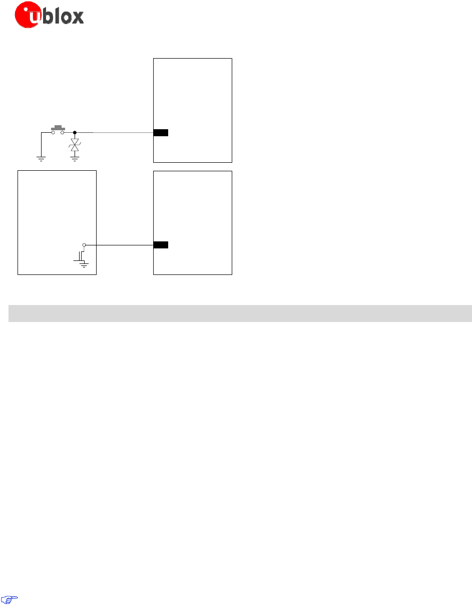
CDMA-2X-11004-3
P
r
e
limin
a
r
y
System de
s
c
r
ipt
ion
Page
19 of 43
LI
S
A-
C
200
&
F
W75-
C
200
-
S
yste
m
I
nte
gra
t
ion
Manual
u-blox
C
200
P
o
w
e
r-on
push
bu
tt
on
ESD
PWR_ON
Appli
c
a
t
ion
P
ro
c
e
ss
or
u-blox C200
O
p
e
n
D
r
a
in
O
u
t
pu
t
P
W
R_
ON
Figure 8: PWR_ON appli
c
a
t
ion
c
i
rcu
i
t
s
using
a
push
button and an open drain output of an appli
c
a
ti
on
proc
e
ss
or
Reference De
sc
ri
pt
ion
Rem
ark
s
ES
D
C
T
0402
S
14A
H
S
G
-
EP
CO
S
Varistor array
for
ESD pro
t
e
c
t
ion
Table
8: Example
of pull-up
resistor
and
ESD pr
ote
c
t
ion for the
PWR_ON appli
c
a
ti
on
c
i
rc
ui
ts
1.5.1.3 Additional
co
n
sid
era
t
ion
s
The
module
is
s
w
i
t
che
d
on when the
vo
l
t
a
ge
rises
up to the
VCC
operating
range:
the
f
ir
s
t
time that the module
is used,
it
is
s
w
i
t
che
d
on in
t
hi
s
way.
Then,
the proper way to
s
w
i
t
ch
off the module
is
by means of the
AT+CPWROFF
command. When the module
is
in power-off mode, i.e. the
AT+CPWROFF
command
has
been
s
e
nt
and a voltage value within the operating range
limi
t
s
is
s
t
ill
provided to the VCC pin, the digital
inpu
t
-
output
pads
of the
baseband
chi
p
s
e
t
(i.e. all the digital
pin
s
of the
module)
are locked in
t
ri-
s
t
a
t
e
(i.e.
f
l
oa
t
ing
)
.
The
power down
t
ri-
s
t
a
t
e
function
i
s
ol
a
t
e
s
the module pins from
i
t
s
environment,
when no proper operation
of
the
ou
t
pu
t
s
can
be guaranteed.
The
module can be
s
w
i
t
che
d
on from power-off mode by forcing a proper
s
t
a
r
t
-up
event (i.e. a falling edge on
the
PWR_ON
pin).
After the detection of a
s
t
a
r
t
-up
event, all the digital pins of the module are held in
t
ri-
s
t
a
t
e
until all the internal
LDO v
ol
t
a
ge
r
e
gul
a
t
ors
are turned on in a defined power-on
sequence. Then, as described
in
Datasheet the
baseband
core
is
s
t
ill
held in
r
e
s
e
t
s
t
a
t
e
for a time interval: the internal
r
e
s
e
t
signal
(which
is
n
ot
available
on a module
pin) is
s
t
ill
low and any
signal
from the module digital
inter
f
ace
s
is
held in
r
e
s
e
t
s
t
a
t
e
.
T
he
r
e
s
e
t
s
t
a
t
e
of all the digital
pin
s
is
reported in the pin
d
e
s
cr
i
ptio
n
table of the
LISA-C200
Data
S
he
e
t
[1] or the
FW75-C200 Data
S
he
e
t
[2]. When the internal
signal is released,
the configuration of the module
inter
f
ace
s
s
t
a
r
t
s
:
during
t
hi
s
phase
any digital pin
is
s
e
t
in a proper
sequence
from the
r
e
s
e
t
s
t
a
t
e
to the default operational
configuration.
F
i
na
ll
y,
the module
is
fully
ready
to
o
pe
r
a
t
e
when all
inter
f
ace
s
are
configured.
The
I
nter
na
l
Re
s
e
t
signal is
not
available
on a module pin.

CDMA-2X-11004-3
P
r
e
limin
a
r
y
System de
s
c
r
ipt
ion
Page
20 of 43
LI
S
A-
C
200
&
F
W75-
C
200
-
S
yste
m
I
nte
gra
t
ion
Manual
1.5.2 Module power
off
The correct
way to
s
w
i
t
ch
off
LISA-C200
&
F
W75-
C
200
modul
e
s
is
by
means
of
+CPWROFF AT
command
(more
de
t
a
il
s
in u-blox C200
AT Commands
Manual [3]): in
t
hi
s
way the current
pa
r
a
me
t
e
r
s
e
tt
ing
s
are
saved
in the
mo
du
l
e
’s
non-volatile
memory
and a proper network
de
t
a
ch
is
performed.
An
under-voltage
s
hu
t
do
w
n
will be done if the
VCC
s
uppl
y
is removed,
but in
t
hi
s
case
the current parameter
s
e
tt
i
ng
s
are not saved
i
n
the
mo
du
l
e
’s
non-volatile
memory
and a proper network
de
t
a
ch
cannot be performed.
1.5.3 Module re
s
e
t
The
module
r
e
s
e
t
can
be performed:
Forcing
a low
level
on the RESET_N input
p
i
n,
ca
u
s
i
ng
an
“
e
xt
e
r
na
l
”
or
“hardware”
reset
(LISA-C200
only)
AT+CFUN
command
(more de
t
a
il
s
in u-blox C200
AT
C
om
ma
nd
s
Manual [3]): in
t
hi
s
case
an
“
i
nte
r
na
l
”
o
r
“software”
reset
is
performed,
caus
i
ng
an asynchronous reset of the
baseband
proce
ss
or
1.6
RF
c
onn
ect
ion
The
ANT
connector has
50 nominal
c
ha
r
a
ct
e
ri
s
t
i
c
impedance
and
mu
s
t
be
connected
to the
antenna
t
hrough
a 50
t
r
ans
mi
ss
ion
line to allow
t
r
ans
mi
ss
ion
and reception of radio
f
r
e
qu
e
ncy
(RF) signals
in the Cell and
P
C
S
operating bands.
Name
Description
Rem
ark
s
A
N
T
F
W75
LISA-C200
RF
connector
Zo
= 50 nominal
c
h
a
r
a
c
t
e
r
ist
i
c
impedance.
U.FL
c
onn
e
c
t
or
S
ur
f
a
c
e
Mount p
a
d
Table
9:
Antenna
c
onnect
or
The
ANT port
ESD
immunity rating
is
500 V
(according
to
IEC
61000-4-2). Higher protection
level
could
be
required
if the line
is externally accessible
on the
application
board.
Choose
an antenna with optimal radiating
c
ha
r
a
ct
e
ri
s
t
i
cs
for the
be
s
t
electrical performance
and
overall
module
functionality.
Focus
on minimizing the
in
s
e
r
t
ion
loss
between radiating antenna and the module
RF
connector.
Overall system
performance
depe
nd
s
on antenna reception and
t
r
ans
mi
ss
ion.
See
s
e
ction
2.4 for further
de
t
a
il
s
regarding antenna
gui
de
li
ne
s
.

CDMA-2X-11004-3
P
r
e
limin
a
r
y
System de
s
c
r
ipt
ion
Page
21 of 43
LI
S
A-
C
200
&
F
W75-
C
200
-
S
yste
m
I
nte
gra
t
ion
Manual
1.7
Serial
communication
LISA-C200
&
F
W75-
C
200
modul
e
s
provide the following
serial
communication
inter
f
ace
s
where
AT
command
interface
and
P
a
ck
e
t
-
S
w
i
t
che
d
D
a
t
a
communication are concurrently
available:
One
a
s
ynchr
ono
us
serial
interface
(UART)
that
prov
id
e
s
RS-232
functionality conforming to
ITU-T
V.24
Re
comm
e
n
da
t
ion
[4], with limited data rate.
One
f
ull-
s
pe
e
d
USB
2.0 compliant
interface,
with
maximum
data rate of 12
Mb/
s
.
Only one interface
is active.
Default
is USB,
if no
USB is
detected
then it
is assumed
that the
UART
interface
i
s
de
s
ir
e
d.
LISA-C200
&
FW75-C200
modul
e
s
are
de
s
ign
e
d
to operate
as
a CDMA
wireless
modem, which
represents
the
data circuit-terminating equipment
(DCE) as described
by the
ITU-T
V.24
Re
co
mm
e
nd
a
t
ion
[4]. A customer
application
processor
connected to the module through one of the
inter
f
ace
s
represents
the data terminal
equipment
(D
T
E
).
All the
inter
f
ace
s
li
s
t
e
d
above are
controlled and
operated
with:
S
prin
t
required AT
Commands
Verizon required AT C
om
ma
nd
s
AT
com
ma
nd
s
according
to
3GPP TS
27.010
[7]
A
T
com
ma
nd
s
according
to 3GPP TS 27.005 [6]
AT
com
ma
nd
s
according
to 3GPP TS 27.010
u-blox
AT
co
mm
a
nd
s
For the complete
li
s
t
of
s
uppor
t
e
d
AT
co
mm
a
nd
s
and their
syntax
refer to the u-blox C200
A
T
C
om
ma
nd
s
Manual [3].
The USB
interface, using all the
lines
provided
(
VUSB_DET
,
USB_D+
and
USB_D-
),
can be used for firmware
upgrade:
To
directly
enable PC (or similar)
connection to the module for firmware upgrade, provide direct
access
on
t
he
application board to the
VUSB_DET
,
USB_D+
and
USB_D-
lines
of the module .
Al
s
o
provide
access
to the
PWR_ON
&
HW_SHUTDOWN
pin
s
,
or
enable
the DC
s
uppl
y
connected
to the
VCC
pin
t
o
s
t
a
r
t
the module firmware upgrade
The
following
s
ub-
cha
pter
s
describe serial
interface configuration
and
provide
a
de
t
a
il
e
d
d
e
s
cr
i
ptio
n
of
each interface
for the
application
c
ir
cui
t
s
.
1.7.1
Serial
inte
rf
a
ce
s
c
onfi
gura
tion
UART
and
USB serial
inter
f
ace
s
are available
as AT
command interface and for
P
a
ck
et-
S
w
i
t
che
d
Data
communication.
The serial
inter
f
ace
s
are configured
as described
in
Table
10
(for
information about
f
urt
he
r
s
e
tt
ing
s
,
please
refer to the u-blox C200
AT Commands
Manual
[3]
)
.
Note :
The UART is
5 wire
implementation
therefore
DTR, DSR
and
DCD
functions
are
not available.

CDMA-2X-11004-3
P
r
e
limin
a
r
y
System de
s
c
r
ipt
ion
Page
22 of 43
LI
S
A-
C
200
&
F
W75-
C
200
-
S
yste
m
I
nte
gra
t
ion
Manual
I
nterfa
c
e AT
S
e
tti
ng
s
Com
me
nt
s
UART
interface
E
n
a
bl
e
d Multiplexing mode can be
enabled
by
AT+CMUX command
providing following channels:
Channel
0: control
c
h
a
nn
e
l
Channel
1:
AT
c
omm
a
nd
s
Channel
2: data
c
onn
e
c
t
ion
A
T
+I
P
R
=1
15200
Baud
rate: 115200 b/
s
A
T
+I
C
F
=0
,0
F
r
a
m
e
format: 8 bits, no parity, 1 stop b
it
USB
interface
E
n
a
bl
e
d
Table
10:
Default
serial i
nterfa
c
e
s
c
onfigurat
ion
1.7.2
As
y
nc
hronou
s
serial i
nte
rfa
c
e (UART)
The UART
interface
is
a 5-wire
unbalanced asynchronous serial
interface that
pro
vi
de
s
AT commands
interface
and
PSD
data communication.
UART
interface
provid
e
s
RS-232
functionality conforming to the
ITU-T
V.24
Re
co
mm
e
nd
a
t
ion
(more
de
t
a
il
s
available
in
ITU
Re
comm
e
nd
a
t
ion
[4]), with
C
MO
S
compatible
signal levels:
0 V for low data bit or ON
s
t
a
t
e
,
and
2.8 V for high data bit or
OFF
s
t
a
t
e
.
One
external
vol
t
a
ge
t
r
ans
l
a
t
ors
(e.g.
Maxim
M
A
X
13234
E
)
could be
used
t
o
provide
RS-232
(5
lines)
compatible
signal levels. This
chip
t
r
ans
l
a
t
e
s
the voltage
levels
from 1.8 V
(module
s
id
e
)
to the
RS-232
s
t
a
nd
a
rd.
For detailed
electrical cha
r
a
ct
e
ri
s
t
i
cs
refer to
LISA-C200
Data
S
he
e
t
[1] or the FW75-
C200
D
a
t
a
S
he
e
t
[2].
FW75-C200 logic levels
are 2.8 V interface.
LISA-C200 logic levels
are 1.8 V interface.
The
LISA-C200
&
FW75-C200
modul
e
s
are
de
s
ig
ne
d
to operate
as
a CDMA
wireless
modem, which
represents
the data circuit-terminating equipment
(DCE) as described
by the
ITU-T
V.24
Re
co
mm
e
nd
a
t
ion
[4]. A
cu
s
t
om
e
r
application
processor
connected to the module through the
UART
interface
represents
the data terminal
equipment
(D
T
E
).
The signal names
of the
LISA-C200
&
F
W75-
C
200
modul
e
s
UART
interface conform to the
ITU-T
V.24
Re
comm
e
n
da
t
ion
[4].
UART
inter
f
ace
s
include
the following
li
ne
s
:
Name De
sc
ri
pt
ion
Rem
ark
s
RI
Ring
Indicator Module ou
t
pu
t
RTS
Ready
to
s
e
nd Module hardware flow control inpu
t
Circuit 105
(Request
to
send)
in
ITU-T
V.24
F
W75 -
Internal
a
c
t
iv
e
pull-up to V_INT
(2.8 V)
interface.
LISA-C200
-
Internal
a
c
t
iv
e
pull-up to
V_INT
(1.8
V) interface.
CTS
Clear
to send Module hardware flow control ou
t
pu
t
Circuit 106
(Ready
for
s
e
nding
)
in
ITU-T
V.24
F
W75-
C
200 -
Internal
a
c
t
iv
e
pull-up to
V_INT
(2.8 V)
interface.
LISA-C200
-
Internal
a
c
t
iv
e
pull-up to
V_INT
(1.8
V) interface.
TxD
T
r
a
n
s
mi
tt
e
d data Module data inpu
t
Circuit 103
(T
r
a
n
s
mi
tt
e
d d
a
t
a
)
in
ITU-T
V.24
Internal
a
c
t
iv
e
pull-up to
V_INT
(2.8
V) enabled.
F
W75-
C
200-
Internal
a
c
t
i
v
e
pull-up to
V_INT
(2.8
V) interface.
LISA-C200
-
Internal
a
c
t
iv
e
pull-up to
V_INT
(1.8
V) interface.
RxD
Received
data Module data
output
Circuit 104
(Received d
a
t
a
)
in
ITU-T
V.24
F
W75-
C
200-
Internal
a
c
t
i
v
e
pull-up to
V_INT
(2.8
V) interface.
LISA-C200
-
Internal
a
c
t
iv
e
pull-up to
V_INT
(1.8
V) interface.
GND Ground
Table
11: UART i
nterfa
c
e
s
ignal
s
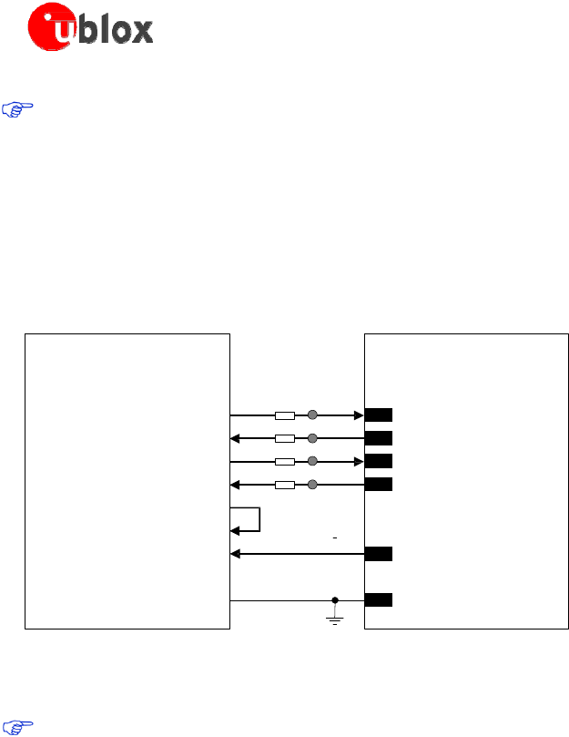
CDMA-2X-11004-3
P
r
e
limin
a
r
y
System de
s
c
r
ipt
ion
Page
23 of 43
LI
S
A-
C
200
&
F
W75-
C
200
-
S
yste
m
I
nte
gra
t
ion
Manual
The UART
interface pins
ESD
s
e
n
s
i
t
i
v
i
t
y
rating
is
1 kV
(Human Body
Model
according
to
J
ES
D
22-A11
4F).
Higher protection
level
could be required if the
lines
are
externally accessible
on the application board.
Higher protection level can be
achieved
by mounting an
ESD
protection (e.g.
EPCOS
C
A05
P
4S
14
T
H
S
G
va
ri
s
t
or
array)
on the
lines connected
to
t
he
s
e
pins.
UART
application
ci
r
cu
it
s
Providing
the TxD,
RxD, RI, RTS
and
CTS lines
only (not
using
the complete V.24 link)
Modem
DSR
,
DCD and
DTR
lines is
not
available
in the application, the application circuit
described
in
Figure
9
mu
s
t
be implemented:
Appli
c
a
ti
on
P
roc
e
ss
or
(D
T
E
)
u-blox C200
(DCE)
TxD
R
xD
R
T
S
C
T
S
D
T
R
D
S
R
RI
D
C
D
GND
0
TP
0
TP
0
TP
0
TP
T
XD
R
XD
RTS
CTS
RI
GND
Figure 9: UART i
nterfa
c
e appli
c
a
ti
on
circuit
with partial V.24 link (5-wire) in the
DTE/DCE serial
c
ommuni
c
a
t
ion
Additional
co
n
sid
era
t
ion
s
I
f
the module
USB
interface
is connected
to the application
processor,
t
e
s
t
poi
nts
can be added on the
li
ne
s
t
o
acc
ommo
da
t
e
the
access
and a 0
series
r
e
s
i
s
t
or
mu
s
t
be mounted on
each
line to detach the
module pin from any other connected
device.
Ot
he
r
w
i
s
e
,
if the
USB
interface
is
not connected to the
application
processor,
it
is
highly recommended to provide direct
access
to
VUSB_DET
,
USB_D+,
USB_D-
lines
for execution of firmware upgrade over
USB
and for debug purpose.
In
both
ca
s
e
s
,
provide
as
well
access
to
RESET_N
pin, or to the
PWR_ON
pin, or
enable
the DC
s
uppl
y
connected
t
o
the
VCC
pin to
s
t
a
r
t
the module firmware upgrade.

CDMA-2X-11004-3
P
r
e
limin
a
r
y
System de
s
c
r
ipt
ion
Page
24 of 43
LI
S
A-
C
200
&
F
W75-
C
200
-
S
yste
m
I
nte
gra
t
ion
Manual
1.7.3
USB
inte
rfa
c
e
LISA-C200
&
FW75-C200
modul
e
s
provide a
f
ull-
s
pe
e
d
USB
interface at 12 Mb/s compliant with the
U
ni
ve
r
s
a
l
Serial Bus Revision
2.0
s
pe
ci
f
i
ca
t
ion
[9].
I
t
acts as
a
USB device
and can be
connected
to any
USB
ho
s
t
such as
a
PC
or other Application
P
r
oce
ss
or.
The USB-device shall
look for all
upper-SW-layers
like any other
serial
device.
This
means that
LISA-C200
&
FW75-C200
modul
e
s
e
mul
a
t
e
all
serial
control
logical
li
ne
s
.
I
f
the
logical DTR
line
i
s
n't
enabled by the
USB
host, the
mo
du
l
e
doesn’t answer to
AT
commands by
t
he
USB
interface.
Name
Description
Rem
ark
s
VUSB_DET
USB
detect input Apply 5 V
typical
to
enable
U
S
B
USB_D+
USB
D
a
t
a
Line
D+ 90 nominal differential impedance.
P
ull-up or pull-down
resistors
and
e
x
t
e
rn
a
l
series resistors
a
s
required by the
USB
2.0
high-speed
sp
e
c
ific
a
t
ion [9] are part
of the
USB
pad
driver
and
need
not be
provided
externally.
USB_D-
USB
D
a
t
a
Line
D- 90 nominal differential impedance.
P
ull-up or pull-down
resistors
and
e
x
t
e
rn
a
l
series resistors
a
s
required by the
USB
2.0
high-speed
sp
e
c
ific
a
t
ion [9] are part
of the
USB
pad
driver
and
need
not be
provided
externally.
Table
12: USB pin
s
The USB
interface pins
ESD
s
ens
i
t
i
vi
t
y
rating
is
1 kV
(Human
Body Model
according
to
J
ES
D
22-A11
4F
).
Higher protection
level
could be required if the
lines
are
externally accessible
on the application board.
Higher protection
level
can be
achieved
by mounting a very low
ca
pa
ci
t
a
nce
(i.e.
less
or equal to 1 pF)
ESD
protection (e.g.
Tyco
E
l
ec
t
roni
cs
PES
D
0402-140
ESD
protection
device)
on the
lines
connected
t
o
t
he
s
e
pin
s
.
LISA-C200
& FW75-C200 module
i
de
ntifi
e
s
i
t
s
e
l
f
by
i
t
s
VID
(Vendor
ID)
and
PID
(P
roduct
ID)
combination,
included
in the
USB device
d
e
s
cr
i
ptor
.
VID
and
PID
of
LISA-C200
&
F
W75-
C
200
modul
e
s
are
the
f
oll
ow
ing:
VID
= 0x1546
PID
= 0x1121
1.7.3.1
USB
application circuit
Since
the module
acts as
a
USB
device, the
USB
s
uppl
y
(5.0 V typ.)
mu
s
t
be provided to
VUSB_DET
by the
connected
USB
ho
s
t
.
The USB
interface
is
enabled only when a valid voltage
as USB
s
uppl
y
is
detected by the
VUSB_DET
input. Neither the
USB
interface, nor the whole module
is
s
uppli
e
d
by the
VUSB_DET
input: the
VUSB_DET
senses
the
USB
s
uppl
y
vo
l
t
a
ge
and
absorbs
few
mi
cr
oa
mp
e
r
e
s
.
The
USB_D+
and
USB_D-
lines carry
the
USB serial
data and
s
ign
a
ling.
The lines
are
used
in
single
ended mode
for
r
e
l
a
t
i
ve
l
y
low
speed
s
ign
a
ling
ha
nd
s
ha
k
e
,
as
well
as
in differential mode for
f
a
s
t
s
ign
a
ling
and data transfer.
USB
pull-up or pull-down
r
e
s
i
s
t
or
s
on pins
USB_D+
and
USB_D-
as required
by the
Universal Serial Bus Revision
2.0
s
pe
ci
f
i
ca
t
ion
[9]
are
part of the
USB
pad
driver
and do not
need
to be
externally
provided.
E
xt
e
r
na
l
series
r
e
s
i
s
t
ors
on pins USB_D+ and USB_D-
as
required by the
Universal Serial Bus Revision
2.0
s
pe
ci
f
i
ca
t
ion
[9] are
also
integrated:
cha
r
a
ct
e
ri
s
t
i
c
impedance
of
USB_D+
and
USB_D-
lines is
s
pe
ci
f
i
e
d
by the
USB
s
t
a
nd
a
rd.
The
mo
s
t
important parameter
is
the differential
cha
r
a
ct
e
ri
s
t
i
c
impedance applicable
f
or
odd-mode
e
l
e
ctrom
a
gn
e
t
i
c
field, which
s
hould
be
as close as possible
to 90 differential:
signal
integrity may
be
degraded
if the
PCB
layout
is
not optimal,
especially
when the
USB
s
ig
na
ling
lines are very
long.
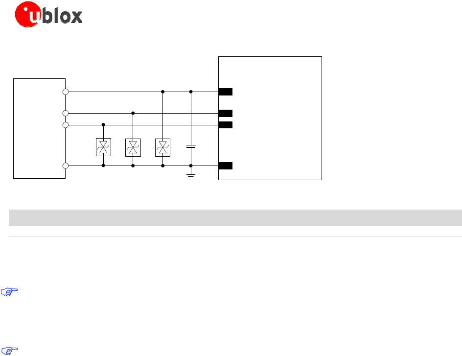
CDMA-2X-11004-3
P
r
e
limin
a
r
y
System de
s
c
r
ipt
ion
Page
25 of 43
LI
S
A-
C
200
&
F
W75-
C
200
-
S
yste
m
I
nte
gra
t
ion
Manual
USB
D
E
VI
C
E
CONN
E
C
T
O
R
u‐blox
C200
V
BU
S
VU
S
B_
D
E
T
D+
U
S
B_
D
+
D- USB_D-
GND
D1 D2 D3 C1
GND
Figure 10: USB I
nterfa
c
e appli
c
a
t
ion
c
ir
c
ui
t
Reference De
sc
ri
pt
ion
Part
Number -
M
anufacturer
D1, D2, D3
Very
L
o
w
Capacitance
ESD
P
ro
t
e
c
t
ion
PES
D
0402-140 -
Tyco
E
l
e
c
t
ron
ic
s
C2 100
nF
Capacitor Ceramic X7R
0402 10% 16 V
G
R
M
155
R
61A104
KA
01 -
M
ur
a
t
a
Table
13:
Component for
USB appli
c
a
ti
on
c
i
rc
ui
t
I
f
the
USB
interface
is
not
connected
to the application
processor,
it
is
highly
recommended
to provide
direct
access
to the
VUSB_DET
,
USB_D+
,
USB_D-
lines
for execution of firmware upgrade over
U
S
B
and for debug
purpo
s
e
:
te
s
t
poi
nts
can
be
added
on the
lines
to
acc
ommo
da
t
e
the
access.
P
r
ov
i
de
acce
ss
to
RESET_N
pin, or to the
PWR_ON
pin, or
enable
the DC
s
uppl
y
connected
to the
VCC
pin to
s
t
a
r
t
the
module firmware upgrade
I
f
the
USB
interface
is
not
used,
the
USB_D+
,
USB_D-
and
VUSB_DET
pin
s
can be left
unconnected,
bu
t
i
t
is
highly
recommended
to
provide
direct
access
to the
lines
for
execution
of firmware
upgrade
and
f
or
debug
purpo
s
e
.
1.7.4 MUX
Protocol (3GPP
27.010)
LISA-C200
&
FW75-C200
modul
e
s
have a
s
oft
w
a
r
e
layer with MUX functionality,
3GPP TS
27.010 Multiplexer
P
rotocol
[7],
a
va
il
a
b
l
e
on the
UART
ph
y
s
i
ca
l
li
nk
.
T
he
USB
i
nte
rf
a
ce
doesn’t support the
mu
l
t
i
pl
e
xer
prot
oco
l
.
This is
a data link protocol (layer 2 of
OSI model)
which
uses HDLC-like
framing and
op
e
r
a
t
e
s
between the
module
(DCE)
and the
application
processor (DTE)
and
a
ll
ow
s
a number of
s
imul
t
a
ne
ou
s
sessions
over the
U
A
RT
:
the user can concurrently use
AT
command interface on one MUX channel and
P
a
ck
e
t
-
S
w
i
t
che
d
Data
communication on another MUX
channel.. Each session
cons
i
s
t
s
of a
s
t
r
ea
m
of
bytes
transferring
various
kind
s
of data
such as SMS, PSD, AT
comm
a
nd
s
in
general. This
pe
rmi
t
s
,
for
example, SMS
to be
t
r
ans
f
e
rr
e
d
to the
D
T
E
when a data
connection is
in
progre
ss
.
The
following virtual
channels are
defined:
Channel
0: control channel
Channel
1:
AT
com
ma
nd
s
Channel
2: data connection
1.8
Reserved pins
(R
S
VD)
LISA-C200
&
F
W75-
C
200
modul
e
s
have
pin
s
reserved
for future use. All the RSVD pins/pads must be
l
e
ft
unconnected
on the
application
board.
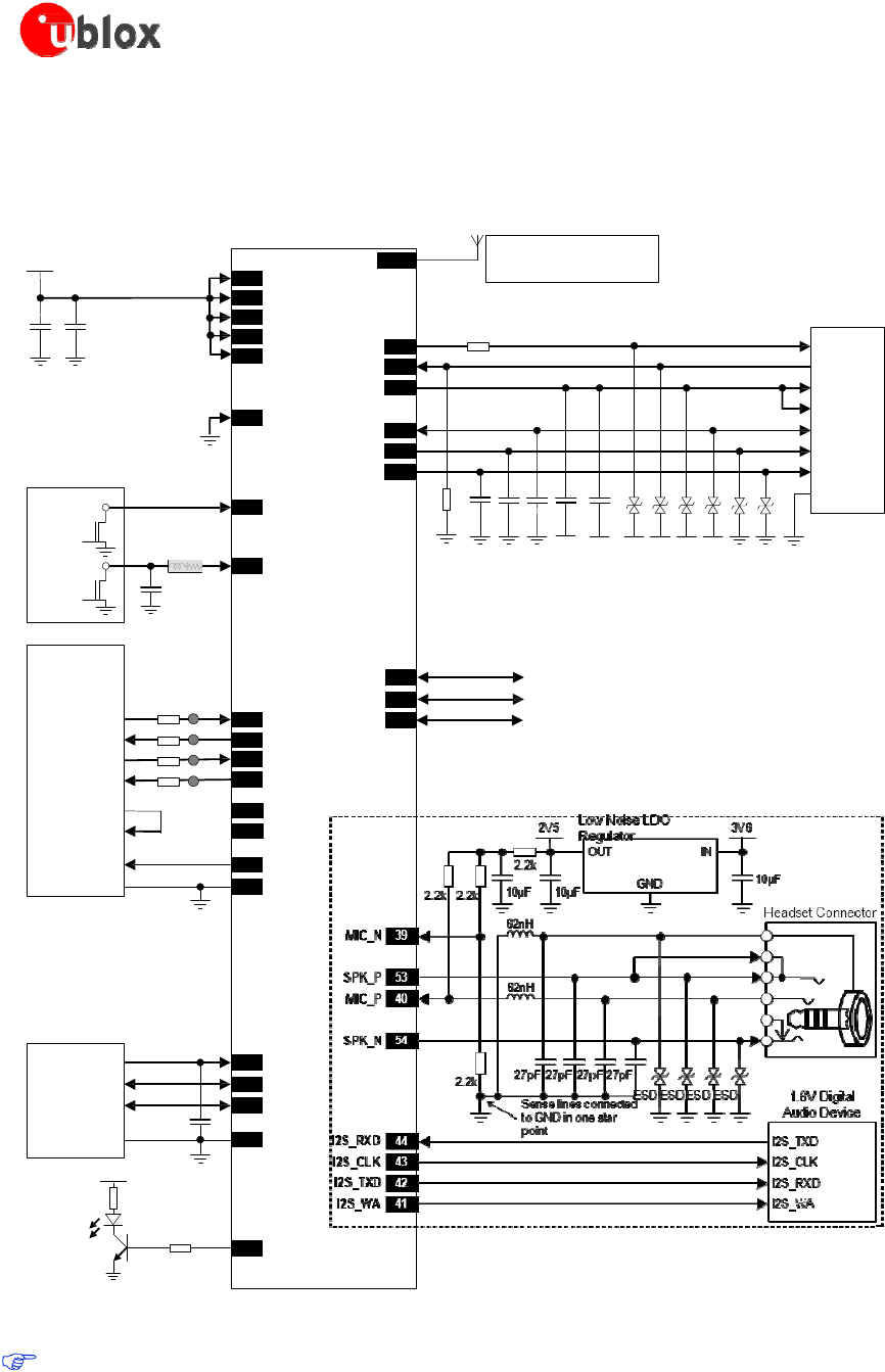
CDMA-2X-11004-3
P
r
e
limin
a
r
y
System de
s
c
r
ipt
ion
Page
26 of 43
LI
S
A-
C
200
&
F
W75-
C
200
-
S
yste
m
I
nte
gra
t
ion
Manual
1.9
Schematic
for
LISA-C200
and
FW75-C200 module
s
in
t
egr
at
ion
Figure
11
s
ho
w
s
the integration of a
LISA-C200
/
FW75-C200
modul
e
s
into an application board, using all the
module
inter
f
ace
s
.
3
V
6
+
22µF
100nF
F
W7
5-
C
200
ANT
VCC
VCC
VCC
VCC V_INT
Antenna
Co
nne
c
ti
on
F
W75
–
U.FL
C
onn
ec
t
or
LISA-C200
SMT
P
A
D
1k
S
I
M
Card
H
old
e
r
SW1
Appli
ca
t
ion
P
ro
ce
ss
or
O
p
en
D
r
ai
n
O
u
t
pu
t
F
er
ri
t
e
Bead
VCC
G
ND
PWR_ON
GPIO5
V
S
I
M
S
I
M
_I
O
SIM_CLK
SIM_RST
470k
47pF 47pF 47pF 47pF 100nF
ESD ESD ESD ESD ESD ESD
SW2
CCVCC
(C1)
CCVPP
(C6)
CCIO
(C7)
CCCLK
(C3)
CCRST
(C2)
GND
(C5)
O
p
en
D
r
ai
n
O
u
t
pu
t
47pF
HW_SHUTDOWN
(
FW7
5-
C
200)
RESET_N
(LISA-C200)
DTE
F
W75
-
2.8V
LISA
–
1.8
V
T
XD
R
XD
R
T
S
C
T
S
D
T
R
DSR
0
TP
0
TP
0
TP
0
TP
T
XD
RXD
RTS
CTS
DTR
DSR
GPIO2
GPIO3
GPIO4
LISA‐C200
only
RI
GND
RI
G
ND
USB
2.0 Host
V
B
U
S
D+
D
-
GND
100nF
VU
SB
_D
E
T
USB_D+
USB_D-
G
ND
3
V
8
N
e
t
w
ork
I
ndi
ca
t
or
GPIO1
Figure 11: Example schematic
integrating
FW75-C200/LISA-C200
module in an appli
c
a
ti
on board, using all the i
nterfa
c
e
s
UART FW75-C200
and
LISA-C200
pins use
different
v
ol
t
a
ge
levels (1.8V LISA-C200,
2.8V
F
W75-
C
20
0)

CDMA-2X-11004-3
P
r
e
limin
a
r
y
System de
s
c
r
ipt
ion
Page
27 of 43
LI
S
A-
C
200
&
F
W75-
C
200
-
S
yste
m
I
nte
gra
t
ion
Manual
1.10 Approval
s
LISA-C200
&
F
W75-
C
200
modul
e
s
have been
or will be
approved
under the following
s
che
me
s
:
CDG1 CDMA
Development
Group 1
Radio
Conformance
T
e
s
t
ing
CDG2 CDMA
Development
Group 2
I
nter-op
e
r
a
bili
t
y
S
prin
t
Carrier
Certification
Verizon Carrier
Certification
FCC
(Federal
C
ommuni
ca
t
ion
s
C
ommi
ss
io
n)
IC
(I
nd
us
t
r
y
C
a
nada
)
1.10.1 Declaration of Conformity for produ
c
ts
marked with the
FCC
logo - U
nit
ed
S
tate
s
only
Radiofrequency radiation exposure
Info
rma
t
ion
:
this equipment
complies
with
FCC
r
adiat
ion
expo
su
re
limits
prescribed
for an uncontrolled environment.
This
equipment
should
be installed
and operated with a minimum
distance
of 20
cm
between the radiator and your body.
1.10.2
M
odifi
c
a
tions
The FCC requires
the
user
to be notified that any
changes
or
modi
f
i
ca
t
ion
s
made to
t
hi
s
device
that are
no
t
expressly approved
by u-blox could void the
user's
authority to
o
pe
r
a
t
e
the equipment.
M
anu
f
act
urer
s
of mobile or fixed devices incorporating the
LISA-C200
&
FW75-C200 modules
are authorized to use the
FCC
Gra
n
t
s
and Industry
Canada Certificates
of the
LISA-C200
&
F
W75
-
C200 modules for their own final
produ
c
t
s
according to the
co
ndi
t
ion
s
referenced in
t
he
certificates.
The
FCC Label shall
in the above
case
be
visible
from the outside, or the
ho
s
t
device shall
bear a
seco
nd
label
s
t
a
t
ing
:
for FW75: “Contains FCC ID: XU9-FW75”
And for LISA C200 “Contains FCC ID: R5Q-LISAC200A”
The IC
Label
shall in the above
case
be visible from the outside, or the host device shall bear a
seco
nd
label
s
t
a
t
ing
for FW75: “Contains IC: 8694A-FW75”
And for LISA C200 “Contains IC: 8595B-LISAC200A”
Canada,
Industry
Canada
(IC) Notices
Changes
or
modi
f
ica
t
ion
s
not
expressly
approved by the party
responsible
for
compliance
could
void the
user's
authority to operate the
equipmen
t
.
Canada, avis
d'I
ndu
s
t
rie
Canada
(IC)
Les
changements ou
mod
if
icat
ion
s
n'ont pas était expressément
approuvé
s
par la
par
t
ie
responsable de la conformité, ils pourraient annulée l'autorité de l'utilisateur pour
explo
it
er
l'é
quipemen
t
.

LI
S
A-
C
200
&
F
W75-
C
200
-
S
yste
m
I
nte
gra
t
ion
Manual
CDMA-2X-11004-3
P
r
e
limin
a
r
y
Design-I
n
Page
28 of 43
2 Design-In
2.1 Design-in checklist
2.1.1
Schematic
c
heck
li
s
t
The
following
are
the
mo
s
t
important points for a
s
impl
e
s
che
ma
t
i
c
check:
DC
s
uppl
y
mu
s
t
provide
a nominal
vo
l
t
a
ge
at
VCC
pin
above
the minimum operating
range
limi
t
.
DC
s
uppl
y
mu
s
t
be
capable
of
s
uppor
t
ing
1.2 A, providing a voltage at
VCC
pin above the minimum
operating
range
limit and with a
maximum
250 mV
vo
l
t
a
ge
drop from the nominal value.
VCC
s
uppl
y
should
be
clean,
with
very
low
rippl
e
/noi
s
e
:
s
ug
ge
s
t
e
d
passive
filtering
pa
r
t
s
can
be
in
s
e
r
t
e
d.
Connect
only one DC
s
uppl
y
to
VCC
:
different
DC
s
uppl
y
systems are
mutually exclusive.
Don’t apply
l
oa
d
s
which
m
i
g
ht
exceed the
li
m
i
t
for maximum
a
va
il
a
bl
e
current from
V_INT
s
uppl
y.
Check
that
vol
t
a
ge
level
of
any connected
pin
does
not
exceed
the
r
e
l
a
t
i
ve
operating range.
C
a
pa
ci
t
a
nce
and
series
r
e
s
i
s
t
a
nce
mu
s
t
be limited on
each
S
I
M
signal
to match the
S
I
M
spe
ci
f
i
ca
t
ion
s
.
I
nse
r
t
the
s
ugg
e
s
t
e
d
low
ca
p
a
ci
t
a
nce
ESD
protection and
passive
filtering
pa
r
t
s
on
each
S
I
M
s
ig
na
l.
Check UART signals
direction,
since
the
signal names
follow the
ITU-T
V.24
Re
com
me
nd
a
t
ion
[4].
P
r
ovi
de
appropriate
access
to
USB
interface and/or to
UART
RxD, TxD
lines
and
access
to PWR_ON
and/or
HW_SHUTDOWN
lines
on the
application
board in order to
fl
a
s
h/up
gra
de
the module firmware.
P
r
ovi
de
appropriate
access
to
USB
interface
and/or to
UART
RxD
,
TxD,
CTS
,
RTS
lines
for debugging.
Add a proper pull-up
re
s
i
s
t
or
to a proper
s
uppl
y
on
each DDC (I
2
C)
interface
line, if the
interface
is
used.
C
a
pa
ci
t
a
nce
and
series
r
e
s
i
s
t
a
nce
mu
s
t
be limited on
each
line of the
DDC
interface.
Use
t
r
ans
i
s
t
ors
with at
l
ea
s
t
an integrated
r
e
s
i
s
t
or
in the
base
pin or
other
w
i
s
e
put a 10 k
r
e
s
i
s
t
or
on
the board in
series
to the
GPIO
when
those are used
to
drive
LE
D
s
.
I
nse
r
t
the
s
ugg
e
s
t
e
d
passive
filtering
pa
r
t
s
on
each used analog
audio line.
P
r
ovi
de
proper
pre
ca
utio
n
s
for
ESD
immunity
as required
on the
application
board.
All
unused pins can
be left floating on the
application
board
Layout
c
heck
li
s
t
The
following
are
the
mo
s
t
important points for a
s
impl
e
layout check:
Check 50 nominal
c
ha
r
a
ct
e
ri
s
t
i
c
impedance of the
RF
t
r
ans
mi
ss
ion
line connected to ANT coax
connector
or
P
rinted
Circuit
Board
50
tr
ans
mi
ss
ion
line
impedance
for
LISA-C200
Follow
the
r
e
comm
e
n
da
t
ion
s
of the
antenna producer
for
correct antenna installation
and deployment.
Ensure
no coupling
occurs
with other
noisy
or
se
n
s
i
t
i
ve
signals (primarily
S
I
M
s
ign
a
l
s
)
.
VCC
line
s
hould
be wide and
s
h
ort
.
Ensure
proper grounding.
C
on
s
i
de
r
“No
-
routing”
areas for the
D
a
t
a
Module
f
oo
t
pri
nt.
Optimize placement
for minimum length of
RF
line and
closer
path from DC
source
for VCC.
Design
USB_D+
/
USB_D-
connection as
90 differential pair.
2.1.2 Antenna
chec
kli
s
t
Antenna
s
hould
have
50
impedance, V.S.W.R less
then 3:1,
recommended
2:1 on operating
bands
in
deployment geographical
area.
Follow the
r
e
co
mm
e
nd
a
t
ion
s
of the antenna producer for correct antenna installation and deployment
(PCB
layout and matching circuitry).
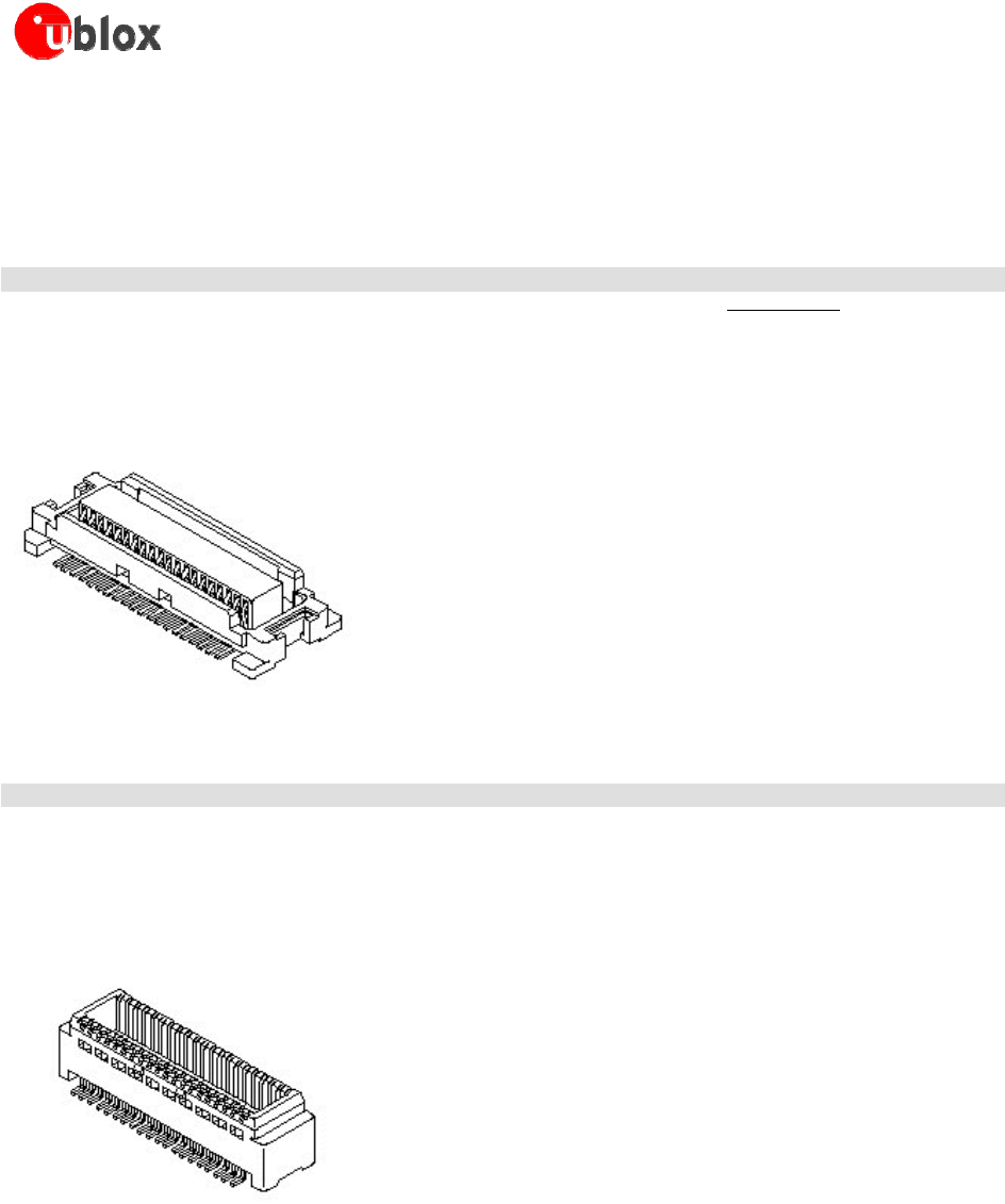
LI
S
A-
C
200
&
F
W75-
C
200
-
S
yste
m
I
nte
gra
t
ion
Manual
CDMA-2X-11004-3
P
r
e
limin
a
r
y
Design-I
n
Page
29 of 43
2.2
Connectors (
F
W75
)
The
following
de
s
ign
information
is
to aid the
de
s
ign
for proper
s
e
l
e
ction
of mating
connectors
and
a
ntenn
a
s
.
2.2.1
FW75-C200
modem
c
onnector
Manufacturer
Series
Name
Part
No.
Specification Description
Rem
ark
s
Molex
S
li
mS
t
a
c
k 52991-0808
PS
-54-167-002
R
e
c
e
p
t
a
c
le
80 pins,
0.50mm pitch, 4mm
stacking
height
Website
: www.mol
e
x
.
c
om
Drawing:
529910708_sd.pdf
(
me
c
h
a
n
ic
a
l,
la
nd pattern and reel
sp
e
c
ifi
c
a
t
ion
s
)
Data
sh
ee
t
:
05339160208_
P
C
B
_
RE
C
EP
T
A
B
L
ES
.
pdf
Table
14: FW75-C200
modem
c
o
nnector
Figure 12: FW75-C200
modem
c
o
nnector
2.2.2
FW75-C200 Board
to Board host connector
Manufacturer
Series
Name
Part
No.
Specification Description
Rem
ark
s
Molex
S
li
mS
t
a
c
k 53916-0808
PS
-54-167-002
Header
80 pins,
0.50mm pitch, 4mm
stacking
height
Website
:
www
.mol
e
x
.
c
om
Drawing:
539160208_sd.pdf
(
me
c
h
a
n
ic
a
l,
la
nd pattern and reel
sp
e
c
ifi
c
a
t
ion
s
)
Data
sh
ee
t
:
05339160208_
P
C
B
_
H
E
A
D
ERS
.
pdf
Table
15: FW75-C200 ho
s
t
mate
c
onne
c
tor
Figure 13: FW75-C200
host mate
c
on
nector

LI
S
A-
C
200
&
F
W75-
C
200
-
S
yste
m
I
nte
gra
t
ion
Manual
CDMA-2X-11004-3
P
r
e
limin
a
r
y
Design-I
n
Page
30 of 43
2.2.3
FW75-C200 RF
antenna
c
onnector
Manufacturer
Series
Name
Part
No.
Specification Description
Rem
ark
s
Molex 73412 73412-0110
PS
-73598-02
Microcoaxial
R
F
,
50 ,
PCB
Vertical
J
a
c
k
R
e
c
e
p
t
a
c
le
,
SMT,
1.25 mm
(
0.049
”
)
M
oun
t
e
d
Height
Website
:
www
.mol
e
x
.
c
om
Drawing:
734120110_sd.pdf
(
me
c
h
a
n
ic
a
l,
la
nd pattern and reel
sp
e
c
ifi
c
a
t
ion
s
)
Data sheet:
0734120110_
RF
_
CO
A
X
_
CONN
E
C
TORS
.
pdf
Table
16: FW75-C200
antenna
c
o
nnector
Figure 14: FW75-C200
antenna
c
onnecto
r
LI
S
A-
C
200
&
F
W75-
C
200
-
S
yste
m
I
nte
gra
t
ion
Manual
CDMA-2X-11004-3
P
r
e
limin
a
r
y
Design-I
n
Page
31 of 43
2.3 Design Guidelines
The
following
de
s
ign
guid
e
li
ne
s
mu
s
t
be met for optimal integration of
LISA-C200
module on the final
application
board.
2.3.1 Layout guideline
s
per pin function
This
s
e
ction
group
s
the u-blox C200 module pins by
signal
function and
provi
de
s
a ranking of importance in
layout
de
s
ign.
See
1:
F
W75-
C
200
2:
LISA-C200
Table
17 for a
li
s
t
of pins
ranked
by their
importance
in layout
de
s
ign.
See
the
LISA-C200
Data
S
he
e
t
[1] or the
FW75 D
a
t
a
S
he
e
t
[2] for the
complete
pin
li
s
t
s
.
Rank
Function Pin(s) Layout
Rem
ark
s
1st
RF
Conn
e
c
tor
2nd Main
DC
S
upply
3rd
USB
S
ignal
s
ANT
V
CC
U
S
B_
D
+
U
S
B_
D-
Very Important
Design
for 50
c
h
a
r
a
c
t
e
r
ist
ic
impedance.
Very Important
VCC
line should be wide and short.
R
ou
t
e
away
from
sensitive analog
signals.
Very Important
R
ou
t
e
USB_D+
and
USB_D- as
differential lines:
design
for 90 differential impedance.
4th Ground GND Careful
Layout
P
ro
v
id
e
proper grounding.
5th
Sensitive Pin :
Careful
Layout
Avoid coupling with
noisy
signals.
P
ower
O
n
H
W
_
S
HU
T
DO
W
N
6th Digital
pins
and
s
upplie
s
:
P
WR_
ON
HW_
S
HU
T
D
OWN
Common
P
r
a
c
t
ic
e
F
ollo
w
common pr
a
c
t
ic
e
rules
for digital pin
rou
t
ing.
SIM Card
Interface
VSIM,
S
IM
_
C
L
K
,
SIM_IO,
S
I
M
_
R
S
T
UART
TXD, RXD, CTS, RTS,
R
I
E
x
t
e
rn
a
l
R
e
s
e
t
H
W
_
S
HU
T
DO
W
N
1
R
ESE
T
_
N
2
General Purpose
I/O2
GPIO1, GPIO2,
G
P
IO
3,
GPIO4,
G
P
IO
5
USB
detection
VU
S
B
_
D
E
T
S
upp
ly
for Int
e
r
f
a
c
e
s
V_
I
N
T
1:
F
W75-
C
200
2:
LISA-C200
Table
17: Pin list
in order of
decreasing
importance for layout de
s
ign

LI
S
A-
C
200
&
F
W75-
C
200
-
S
yste
m
I
nte
gra
t
ion
Manual
CDMA-2X-11004-3
P
r
e
limin
a
r
y
Design-I
n
Page
32 of 43
2.4 Antenna guideline
s
Antenna
cha
r
a
ct
e
ri
s
t
i
cs
are
essential
for good functionality of the module. Antenna radiating
performance
ha
s
direct impact on the
reliability
of
connections over
the Air
I
nter
f
ace
.
A bad termination of ANT
can
r
e
s
ul
t
in poor
performance
of the module.
The
following
pa
r
a
me
t
e
r
s
s
hould
be
che
ck
e
d:
Item Recommendations
Impedance 50 nominal
c
h
a
r
a
c
t
e
r
ist
ic
impedance
Frequency
Range
Depends
on the Mobile Network u
s
e
d.
LISA-C200
:
- Cell
Band B0:
824..894 MHz
-
PCS Band B1 B2:
1850..1990 MHz
Input
Power
>2 W peak
V.S.W.R
<2:1
recommended,
<3:1 acceptable
Return
Loss
S
11
<
-10
dB recommended,
S
11
<
-6
dB
acceptable
Gain <3 d
B
i
Table
18:
General re
c
omme
ndat
ion for CDMA a
nte
nna
To
preserve
the original u-blox
FCC
ID, antenna gain
shall
remain below 3 dBi.
CDMA
a
ntenn
a
s
are
t
ypi
ca
ll
y
available
a
s
:
Linear monopole: typical for fixed
a
ppli
ca
t
ion
s
.
The
antenna
extends
mo
s
t
l
y
as
a linear element with a
di
me
n
s
ion
comparable
to lambda/4 of the
l
ow
e
s
t
f
r
e
qu
e
ncy
of the operating band. Magnetic
base
may be
available. Cable or direct
RF
connectors are common
op
t
ion
s
.
The
integration normally
requires
the
fulfillment of
some
minimum
gui
de
li
ne
s
s
ug
ge
s
t
e
d
by
antenna
manufacturer
P
a
t
ch
-lik
e
antenna: better
s
ui
t
e
d
for integration in compact
designs
(e.g. mobile phone).
These
are
mo
s
t
l
y
custom
designs
where the exact definition of the
PCB
and product
mechanical
de
s
ign
is
fundamental
f
or
tuning of
antenna
cha
r
a
ct
e
ri
s
t
i
cs
For
integration
observe
t
he
s
e
r
e
comm
e
nd
a
t
ion
s
:
Ensure
50 antenna termination by minimizing the
V.S.W.R.
or return
loss, as
t
hi
s
will optimize the
electrical performance
of the module.
See
s
e
ction
2.4.1
S
e
l
e
ct
antenna
with
b
e
s
t
radiating
performance.
See
s
e
ction
2.4.2
I
f
a cable
is
used to connect the antenna radiating element to application board,
select
a
s
hor
t
cable
w
i
t
h
minimum
in
s
e
r
t
ion
loss. The
higher the additional insertion
loss
due to low quality or long
cable,
the lower
the connectivity
Follow
the
r
e
comm
e
n
da
t
ion
s
of the
antenna manufacturer
for correct
installation
and deployment
Do not
include antenna
within
closed
metal
ca
s
e
Do not place antenna in
close
vicinity to end
user since
the emitted radiation in human
t
i
ss
ue
is
limited by
S.A.R.
regulatory
requirements
Do not
use directivity antenna
since
the
e
l
e
ctrom
a
gn
e
t
i
c
field radiation
intensity
is
limited in
some
co
un
t
ri
e
s
Take
care of interaction between co-located
RF systems since
the
RF
transmitted power may interact or
di
s
t
urb
the
performance
of
companion
s
yste
m
s
Place
antenna far from
s
ens
i
t
i
ve
analog
s
y
s
t
e
ms
or employ
cou
nter
me
a
s
ure
s
to reduce electromagnetic
compatibility
issues
that
may
a
ri
s
e
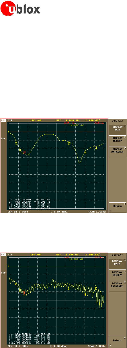
LI
S
A-
C
200
&
F
W75-
C
200
-
S
yste
m
I
nte
gra
t
ion
Manual
CDMA-2X-11004-3
P
r
e
limin
a
r
y
Design-I
n
Page
33 of 43
2.4.1 Antenna
te
rmina
tion
The
LISA-C200
&
F
W75-
C
200
modul
e
s
are
de
s
ign
e
d
to work on a 50 load.
However,
real
a
ntenn
a
s
have no
perfect 50 load on all the
s
upp
ort
e
d
f
r
e
qu
e
ncy
ba
nd
s
.
T
he
r
e
f
ore
,
to
reduce as
much
as possible
performance
degradation
due to
antenna
mi
s
ma
t
ch,
the following
r
e
quir
e
me
n
t
s
s
hould
be met:
Me
a
s
ure
the antenna termination with a network
analyzer:
connect the antenna through a
coaxial cable
to the
me
a
s
ureme
nt
device,
the
|S
11
|
indi
ca
t
e
s
which portion of the power
is delivered
to antenna and which portion
i
s
reflected
by the
antenna back
to the module
ou
t
pu
t
.
A good antenna
s
hould
have an
|S
11
|
below -10
dB
over the entire frequency band. Due to miniaturization,
mechanical
con
s
t
r
a
i
nts
and other
de
s
ign
issues,
t
hi
s
value
will not be
achieved.
An
|S
11
| value
of about -6 dB –
(
in
the worst
case)
-
is
acceptable.
Figure
15
s
h
ow
s
an
example
of
t
hi
s
me
a
s
ureme
nt:
Figure 15: |S
11
| sample mea
s
ureme
nt
of a penta-band antenna that
covers
in a
small
form
fa
c
tor
the 4 bands (850 MHz, 900
M
Hz,
1800 MHz and 1900
M
Hz)
Figure
16
s
h
ow
s
comparable
me
a
s
urements
performed on a wideband antenna.
The
termination
is
better,
bu
t
the
size
of the
antenna is considerably
larger.
Figure 16: |S
11
| sample mea
s
ureme
nt
of a wideband a
nte
nna
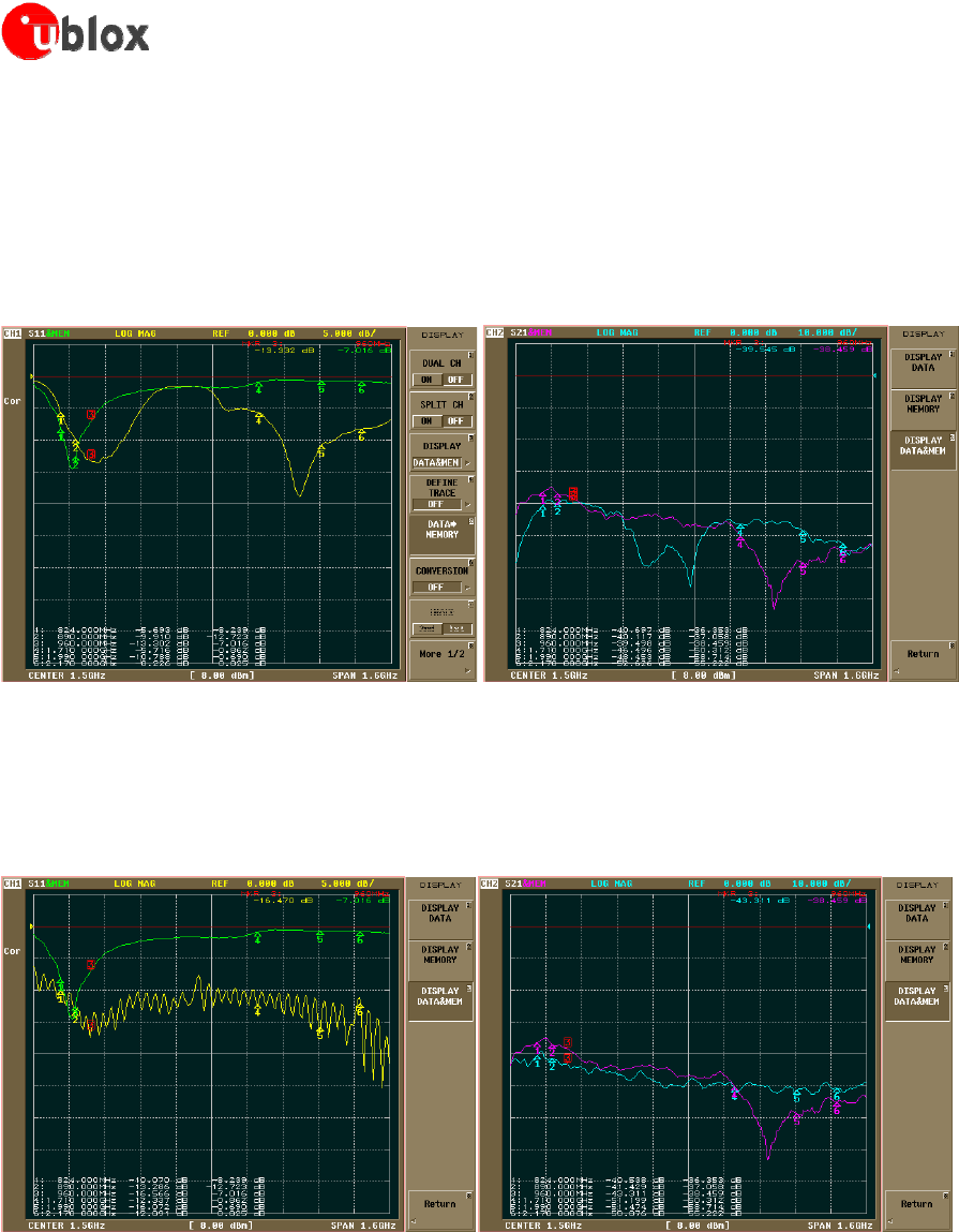
LI
S
A-
C
200
&
F
W75-
C
200
-
S
yste
m
I
nte
gra
t
ion
Manual
CDMA-2X-11004-3
P
r
e
limin
a
r
y
Design-I
n
Page
34 of 43
2.4.2 Antenna radia
tion
An
i
nd
i
ca
t
i
on
of the
antenna’s
radiated power can be
approximated
by measuring the |S21| from a target antenna
to the
me
a
s
ureme
nt
antenna, using a network
analyzer
with a wideband antenna.
Me
a
s
urements
s
hould
be
done at a fixed
di
s
t
a
nce
and orientation, and
r
e
s
ul
t
s
compared
to
me
a
s
urements
performed on a known good
antenna.
Figure
17 through
Figure
18
s
ho
w
me
a
s
ure
m
e
nt
r
e
s
ul
t
s
.
A wideband log periodic-like antenna
w
a
s
used,
and the
com
pa
ri
s
on
w
a
s
done with a half
lambda
dipole tuned at 900 MHz
f
r
e
qu
e
ncy.
The
me
a
s
urements
s
ho
w
both the
|S
11
|
and
|S
21
|
for the
penta-band
internal
antenna
and for the wideband antenna.
Figure 17: |S
11
|
and
|S
21
| comparison
between a 900 MHz tuned half wavelength dipole (green/purple) and a penta-band i
nte
rnal
antenna (yello
w
/cyan)
The
half lambda dipole tuned at 900 MHz
is
known and
has
good radiation performance (both for gain and
dir
e
cti
vi
t
y).
Then,
by
comparing
the
|S
21
|
me
a
s
ureme
nt
with
antenna
under
i
nve
s
t
i
ga
t
ion
for the
f
r
e
qu
e
ncy
where
the half dipole
is
tuned (e.g.
marker
3 in
Figure 17)
it
is possible
to make a judgment on the
antenna
under
t
e
s
t
:
if the
performance
is
s
imil
a
r
then the target
antenna is
good.
Figure 18: |S
11
|
and
|S
21
| comparison
between a 900 MHz tuned half wavelength dipole (green/purple) and a
w
ideband
commercial
antenna (yello
w
/cyan)
I
ns
t
ea
d
if
|S
21
| values
for the tuned dipole are much better than the
antenna
under
eva
l
ua
t
ion
(like
for
marker
1/2
area of
Figure
18, where dipole
is
5 dB better), then it can be argued that the radiation of the target antenna
(the wideband dipole in
th
i
s
case) is
c
on
s
i
de
r
a
bl
y
l
e
ss
.
The same procedure
s
hould
be
r
e
pe
a
t
e
d
on other
bands
with half
wavelength
dipole re-tuned to the band under
i
nve
s
t
i
ga
t
ion.

LI
S
A-
C
200
&
F
W75-
C
200
-
S
yste
m
I
nte
gra
t
ion
Manual
CDMA-2X-11004-3
P
r
e
limin
a
r
y
Design-I
n
Page
35 of 43
For
good
antenna
radiation
performance, antenna
di
me
ns
ion
s
s
hould
be
comparable
to a quarter of the
wavelength. Different antenna
t
ype
s
can be used for the module, many of them (e.g. patch
a
ntenn
a
s
,
monopole)
are
based
on a
r
e
s
on
a
t
ing
element that
w
ork
s
in combination with a ground plane.
T
he
ground plane, ideally infinite, can be reduced down to a minimum
size
that
mu
s
t
be
s
imil
a
r
to one
quarter of the wavelength of the minimum frequency that
has
to be radiated
(tr
ans
mi
tt
e
d/re
ce
i
ve
d).
Numerical sample:
f
r
e
qu
e
nc
y
= 1 GHz wavelength = 30 cm minimum ground plane (or antenna
size)
= 7.5 cm.
Below
t
hi
s
size,
the
antenna
e
ff
i
ci
e
ncy
is
reduced.
2.5
ESD
immunity test pr
ecau
t
ion
s
The
immunity of the device (i.e. the application board where
LISA-C200
&
F
W75-
C
200
module
is
mounted)
E
l
e
ctr
os
t
a
t
i
c
Discharge
mu
s
t
be certified in compliance to the
t
e
s
t
ing
requirements
s
t
a
nd
a
rd
[12], and the
requirements
for radio and digital
cellular
radio
telecommunications
system
equipment
s
t
a
nd
a
r
ds
[12] and [14].
The ESD
t
e
s
t
is
performed at the
enclosure
port referred to
as
the
physical boundary
through which the
E
M
field
r
a
di
a
t
e
s
.
I
f
the
device implements
an integral antenna, the
enclosure
port
is seen as
all
in
s
ul
a
t
ing
and conductive
surfaces
housing the
device.
I
f
the
device implements
a
removable
antenna, the antenna port can be
s
e
pa
r
a
t
e
d
from the enclosure port.
The
antenna port
comprises
the antenna element and
i
t
s
interconnecting cable
s
urf
ace
s
.
The
applicability of the
ESD
t
e
s
t
depe
nd
s
on the device
cl
a
ss
i
f
i
ca
t
ion,
as
well the
t
e
s
t
on other
por
t
s
or on
interconnecting
cables
to auxiliary equipments
depe
nd
s
to the device
accessible
inter
f
ace
s
and manufacturer
requirements.
Contact
discharges
are performed at conductive
surfaces
w
he
r
ea
s
air
discharges
are performed on
in
s
ul
a
t
ing
surfaces.
I
ndir
e
ct
contact
discharges
are performed on the
me
a
s
ureme
nt
s
e
t
up
horizontal and
ve
r
t
i
ca
l
coupling
pl
a
ne
s
.
I
mpl
e
me
nt
the following
pr
eca
u
t
ion
s
to
s
a
t
i
s
f
y
ESD
immunity
t
e
s
t
requirements performed at the device
enclosure
in
compliance
to the
ca
t
e
gor
y
level
and
s
ho
w
n
in the following table.
Appli
c
a
ti
on Category Immunity
L
evel
All
exposed
su
r
f
a
c
e
s
of the radio equipment and ancillary equipment
in a r
e
pr
e
se
n
t
a
t
iv
e
c
on
f
igur
a
t
ion
Contact Discharge 4 kV
Air Discharge 8 kV
Table
19
:
E
l
e
c
tro
m
a
g
net
ic
Compatibility
(EMC) ESD
immunity
r
e
qui
rem
e
nt,
standards
“EN
61000-4-2,
EN
301 489-1 V1.8.1,
E
N
301 489-7
V
1.3.1
”
Although
E
MC
certification (including
ESD
immunity
t
e
s
t
ing
)
must be performed in the final application of the
radio equipment
EUT,
r
e
s
ul
t
s
are provided for
LISA
modul
e
s
performing the
t
e
s
t
with a
r
e
pre
s
e
nta
t
i
ve
configuration to
s
ho
w
that
requirements can
be met.
Since
an external antenna
is used,
the antenna port can be
s
e
pa
r
a
t
e
d
from the
enclosure
port.
The
reference
application
is
not
enclosed
in a box
so
the
enclosure
port
is
not indentified with
physical surfaces.
T
he
r
e
f
ore
,
some
t
e
s
t
cases
cannot be
applied. Only
the
antenna
port
is
identified
as accessible
for direct
ESD
exposure.
The
r
e
f
e
r
e
nce
application
impl
e
me
nt
s
all
precautions described
in the
sections
below.
ESD
immunity
t
e
s
t
r
e
s
ul
t
s
and
a
ppli
ca
bili
t
y
are
reported in
Table
20
according
to
t
e
s
t
requirements
[12], [12] and [14].

LI
S
A-
C
200
&
F
W75-
C
200
-
S
yste
m
I
nte
gra
t
ion
Manual
CDMA-2X-11004-3
P
r
e
limin
a
r
y
Design-I
n
Page
36 of 43
Category Appli
c
a
ti
on Immunity
L
evel
Contact
Discharge
to coupling
planes
(indirect
contact
discharge)
E
n
c
losu
r
e
+2 kV / -2 kV
+4 kV / -4 kV
Contact
Discharges
to
conducted
s
ur
f
a
c
e
s
(
dir
e
c
t
contact
discharge)
E
n
c
losu
r
e
port Not Applicable5
Contact
Discharges
to conducted
s
ur
f
a
c
e
s
(
dir
e
c
t
contact
discharge)
Antenna por
t
(only
antenna with completely
insulating
su
r
f
a
c
e
can
be u
se
d
)
Not Applicable6
Air
Discharge
at insulating
su
r
f
a
c
e
s
E
n
c
losu
r
e
port Not Applicable7
Air
Discharge
at insulating
su
r
f
a
c
e
s
Antenna por
t
(only
antenna with
c
ompl
e
t
e
l
y
+2 kV / -2 kV
+4 kV / -4 kV
insu
la
t
ing
su
r
f
a
c
e
c
a
n b
e
u
se
d
)
+8 kV / -8 k
V
Table
20
:
E
n
cl
o
s
ure
ESD
immunity
level result,
standards
“EN
61000-4-2,
EN
301 489-1 V1.8.1,
EN
301 489-7 V1.3.1” for
L
I
SA
appli
c
a
ti
on reference design.
2.5.1 General pre
c
a
utions
The
following module
inter
f
ace
s
can have a critical influence in
ESD
immunity
t
e
s
t
ing,
depending on the
application
board handling.
The
following
pre
ca
utio
n
s
are
s
ug
ge
s
t
e
d:
HW_SHUTDOWN pin
(FW75-C200
only)
S
ens
i
t
i
ve
interface
is
the
r
e
s
e
t
line
(
HW_SHUTDOWN
pin):
A 47
pF bypass
ca
pa
ci
t
or
(e.g. Murata
GRM1555C1H470JA01) have
to be mounted on the line termination
connected to the HW_SHUTDOWN pin to avoid a module
r
e
s
e
t
caused by an electrostatic
di
s
c
ha
r
ge
applied
to the
application
board enclosure
A
series
ferrite bead (e.g. Murata
BLM15HD182SN1)
mu
s
t
be added on the line connected to the
HW_SHUTDOWN pin to avoid a module
r
e
s
e
t
caused by an electrostatic
discharge
applied to the
application
board enclosure
I
t
is recommended
to
keep
the
connection
line to
HW_SHUTDOWN
as
s
hor
t
as
po
ss
ibl
e
Reset_N pin
(LISA-C200
only)
S
ens
i
t
i
ve
interface
is
the
r
e
s
e
t
line
(
Reset_N
pin):
A 47
pF bypass
ca
pa
ci
t
or
(e.g. Murata
GRM1555C1H470JA01) have
to be mounted on the line termination
connected
to the Reset_N pin to avoid a module
r
e
s
e
t
caused
by an
e
l
e
ctr
os
t
a
t
i
c
discharge
applied to the
application
board enclosure
A
series
ferrite bead (e.g. Murata
BLM15HD182SN1)
must be added on the line
connected
to the Reset_N
pin to
avoid
a module
r
e
s
e
t
caused
by an
e
l
e
ctr
os
t
a
t
i
c
discharge applied
to the
application
board
e
nc
lo
s
ure
I
t
is recommended
to
keep
the
connection
line to Reset_N
as
s
h
ort
as
po
ss
ibl
e
5
LISA
mounted on application design:
Not
Applicability
->
EUT
with insulating
enclosure
su
r
f
a
c
e
,
EUT
without
enclosure
surface
Applicability ->
EUT
with
conductive enclosure
surface
6
LISA
mounted on application design:
Not
Applicability
-> Antenna with insulating surface
Applicability -> Antenna with
conductive
surface
7
LISA
mounted on application design:
Applicability ->
EUT
with
insulating enclosure
surface
Not
Applicability
->
EUT
with
conductive enclosure
su
r
f
a
c
e
,
EUT
without
enclosure
surface
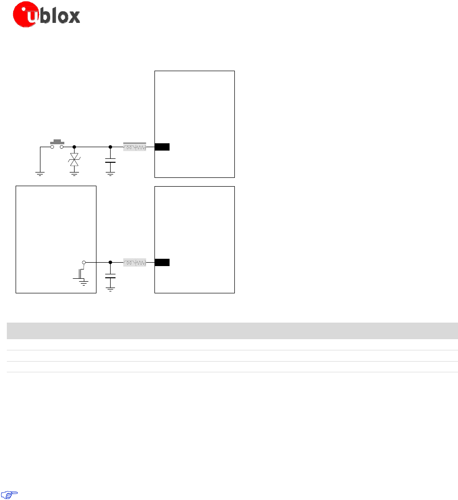
LI
S
A-
C
200
&
F
W75-
C
200
-
S
yste
m
I
nte
gra
t
ion
Manual
CDMA-2X-11004-3
P
r
e
limin
a
r
y
Design-I
n
Page
37 of 43
u-blox
C
200
R
es
et
push
bu
tt
on
ESD
F
B
1
C1
H
W
_S
HU
T
DO
W
N
Appli
c
a
t
ion
P
ro
c
e
ss
or
u-blox C200
Open
Drain
O
u
t
pu
t
F
B
2
H
W
_S
HU
T
DO
W
N
C2
Figure 19: HW_SHUTDOWN appli
c
a
ti
on
c
ir
c
ui
t
s
for
ESD
immunity
te
s
t
Reference De
sc
ri
pt
ion
Rem
ark
s
ES
D
Varistor
for
ESD pro
t
e
c
t
ion.
C
T
0402
S
14A
H
S
G
-
EP
CO
S
C1, C2 47
pF
Capacitor Ceramic
C0G 0402 5% 50 V
G
R
M
1555
C
1
H
470
J
A01 -
M
ur
a
t
a
FB1,
F
B
2 Chip
F
e
rrite
Bead
for
N
o
is
e
/
E
M
I
S
uppr
e
ssio
n
B
L
M
15
HD
182
S
N
1 -
M
ur
a
t
a
R
int
10 k
Resistor
0402 5% 0.1 W
Internal
pull-up resistor
Table
21: Example
of
c
omponen
ts
as ESD
immunity
te
s
t
pre
c
a
ut
i
ons
for the
HW_SHUTDOWN
line
SIM interface
S
ens
i
t
i
ve
interface
is
the
S
I
M
interface (
VSIM
pin,
SIM_RST
pin, SIM_IO pin,
SIM_CLK
pin):
A 47 pF
bypass ca
pa
ci
t
or
(e.g. Murata
GRM15
55
C
1
H
470
J
)
have to be mounted on the
lines connected
t
o
VSIM,
SIM_RST
,
SIM_IO and
SIM_CLK
to
assure
S
I
M
interface
functionality when an
e
l
e
ctr
os
t
a
t
i
c
di
s
c
ha
r
ge
is applied
to the
application
board
e
ncl
o
s
ure
I
t
is
s
ugg
e
s
t
e
d
to
use as
s
hor
t
as possible connection lines
at
S
I
M
pins
S
I
M
card interface
is hardware ready
but not
s
uppor
t
e
d
by the current
s
oft
w
a
r
e
2.5.2 Antenna i
nte
rf
a
c
e pre
c
a
utions
The
antenna interface ANT can
have
a critical influence on the
ESD
immunity
t
e
s
t
depending
on the application
board handling. Antenna
precaution
s
ug
ge
s
t
ion
s
are
provided:
I
f
the
device
impl
e
me
nt
s
an
embedded
antenna and the
device
insulating
enclosure avoids
air
discharge
up
t
o
+8 kV / -8 kV to the
antenna interface,
no further
precautions
to
ESD
immunity
t
e
s
t
s
hould
be needed
I
f
the
device implements
an
external
antenna and the antenna and
i
t
s
connecting
cable
are provided with a
comp
l
e
t
e
l
y
insulating
enclosure
to avoid air
discharge
up to +8 kV / -8 kV to the whole antenna and cable
surfaces,
no further
pre
ca
uti
on
s
to
ESD
immunity
t
e
s
t
s
hould
be needed

LI
S
A-
C
200
&
F
W75-
C
200
-
S
yste
m
I
nte
gra
t
ion
Manual
CDMA-2X-11004-3
P
r
e
limin
a
r
y
Design-I
n
Page
38 of 43
I
f
the
device implements
an
external antenna
and the
a
n
t
e
nn
a
or
i
t
s
connecting cable
are not
provided
w
i
t
h
comp
l
e
t
e
l
y
insulating
enclosure
to avoid air
discharge
up to +8 kV / -8 kV to the whole antenna and cable
surfaces,
the following
pr
eca
utio
n
s
to
ESD
immunity
t
e
s
t
s
hould
be
implemented
on the
application
board
A higher protection
level is
required at the ANT port if the line
is externally accessible
on the application board.
ESD
immunity
t
e
s
t
requires
protection up to +4 kV / -4 kV for direct Contact
Discharge
and up to +8 kV / -8 kV
for Air
Discharge applied
to the
antenna
por
t
.
2.5.3 Module i
nte
rfa
c
e
s
pre
c
a
utions
All the module pins that are
externally accessible
s
hould
be included in the
ESD
immunity
t
e
s
t
since
they are
considered
to be a port
as
defined in [12].
Depending
on
applicability,
and in order to
s
a
t
i
s
f
y
ESD
immunity
t
e
s
t
requirements
and
ESD
category level,
pin
s
connected
to the port
s
hould
be protected up to +4 kV / -4 kV
f
or
direct Contact
Discharge,
and up to +8 kV / -8 kV for Air
Discharge applied
to the
enclosure
s
urf
ace
.
The
maximum
ESD
s
ens
i
t
i
vi
t
y
rating of all the pins of the module, except the ANT pin,
is
1 kV (Human
B
od
y
Model
according
to
J
ES
D
22-A11
4F
).
A higher protection level can be
achieved
by mounting an
ESD
protection
(e.g. EPCOS
C
A05
P
4S
1
4T
H
S
G
va
ri
s
t
or
array
or
C
T
040
2S
14A
H
S
G
).
For the
USB
interface a very low
ca
pa
ci
t
a
nce
(i.e.
less
or equal to 1 pF)
ESD
protection (e.g.
Tyco
E
l
e
ctroni
c
s
PES
D
0402-140
ESD
protection
device) can
be mounted on the
lines connected
to
USB_D+
and
USB_D-
pin
s
.
For the
S
I
M
interface a low
ca
pa
ci
t
a
nce
(i.e.
less
than 10
pF) ESD
protection (e.g.
I
nfin
e
on
ESD8V0L2B-03L
or
AVX U
S
B
000
2)
must be
placed near
the
S
I
M
card
holder on
each
line
(
VSIM
,
SIM_IO
,
SIM_CLK
,
SI
M
_
R
ST
).

LI
S
A-
C
200
&
F
W75-
C
200
-
S
yste
m
I
nte
gra
t
ion
Manual
CDMA-2X-11004-3
P
r
e
limin
a
r
y
F
ea
t
ur
e
s
d
e
s
c
r
ipt
ion
Page
39 of 43
3
Features
description
3.1
F
ir
mw
are (upgrade) Over The Air (FOTA
LISA-C200
&
F
W75-
C
200
modul
e
s
will
s
uppor
t
t
hi
s
feature.
S
prin
t
Carrier
r
e
quir
e
m
e
nt.
N
ot
s
upp
ort
e
d
nor
required
for
Verizon
Carrier.
3.2 UDP/I
P
LISA-C200
&
F
W75-
C
200
modul
e
s
will
s
uppor
t
t
hi
s
feature in the upcoming
FW ve
r
s
ion.
3.3 HTTP
LISA-C200
&
F
W75-
C
200
modul
e
s
will
s
uppor
t
t
hi
s
feature in the upcoming
FW ve
r
s
ion.

LI
S
A-
C
200
&
F
W75-
C
200
-
S
yste
m
I
nte
gra
t
ion
Manual
CDMA-2X-11004-3
P
r
e
limin
a
r
y
Appendix
Page
40 of 43
Appendix
A Glossary
ADC Analog to Digital Converter
AP Application
P
r
oc
e
ss
or
AT AT Command
Interpreter
S
o
ftw
a
r
e
S
u
bs
y
s
t
e
m, or
a
tt
e
nti
on
CBCH Cell
Br
oadc
a
s
t
Channel
CS Coding
S
ch
e
m
e
CSD Circuit
S
wit
ch
e
d Data
CTS
Clear To
S
e
nd
DC
Direct
Current
DCD Data
Carrier
Detect
DCE Data Communication
E
quipm
e
nt
DCS Digital
Cellular
S
ys
tem
DDC
Display
Data Channel
DSP
Digital
S
ign
a
l
P
r
oc
e
ss
ing
DSR
Data
S
e
t
R
ea
dy
DTE
Data
Terminal
E
quipm
e
nt
DTM
Dual
T
r
a
n
s
f
e
r
Mod
e
DTR
Data
Terminal
R
ea
dy
EBU
E
xt
e
rn
a
l
Bus Interface
Uni
t
CDMA
CODE Division
Multiple
Acc
e
ss
FDD
Frequency Division
Duplex
FEM
Front End
Module
FOAT
Firmware Over AT
com
m
a
nd
s
FTP
File Transfer
P
rotocol
FTPS
FTP S
e
cu
re
GND Ground
GPIO
General
P
urpo
s
e
Input
Output
GPS
Global
P
o
s
itio
ning
S
y
s
tem
HF Hands-free
HTTP
Hyp
e
rT
e
x
t
T
r
a
n
s
f
e
r
P
roto
col
HTTPS
Hypertext Transfer
P
rot
ocol
over Secure
S
o
ck
e
t
L
a
y
e
r
HW Hardware
I/Q In
phase
and Quadrature
I
2
C
Inter-Integrated
Circuit
I
2
S
Inter
IC
S
ound
IP
Internet
P
rotocol
IPC
Inter
Processor
Communication
LNA Low
Noise Am
plifi
e
r
MCS Modulation Coding
S
ch
e
m
e
NOM Network
Operating
Mode

LI
S
A-
C
200
&
F
W75-
C
200
-
S
yste
m
I
nte
gra
t
ion
Manual
CDMA-2X-11004-3
P
r
e
limin
a
r
y
Appendix
Page
41 of 43
PA
P
ow
e
r Amp
lifi
e
r
PBCCH
P
a
ck
e
t
Br
oadc
a
s
t
Control Channel
P
CM
Pulse
Code
Mod
ula
tion
PCS
Personal
Com
muni
ca
tion
s
S
e
rv
ic
e
PFM
Pulse
F
re
qu
e
ncy
M
odul
a
ti
on
P
MU
P
ow
e
r
Management
Un
it
RF
Radio
F
re
qu
e
ncy
RI
Ring
Indicator
RTC
Real Time
Clock
RTS
Re
qu
e
s
t
To
S
e
nd
RXD
RX
Data
S
AW
S
urf
a
c
e
Acoustic
Wave
SIM
S
ub
s
cribe
r
I
de
ntifi
ca
t
ion Module
SMS
S
hor
t
Message
S
e
rvic
e
SMTP
S
impl
e
Mail
T
ra
ns
f
e
r
P
rot
ocol
SRAM
S
t
a
tic RAM
TCP Transmission
Control
P
rotocol
TDMA Time Division
Multiple
Ac
ce
ss
TXD TX
Data
UART
Universal A
s
y
nchro
nou
s
R
e
c
e
iv
e
r-
T
r
a
n
s
m
itt
e
r
UDP
User
Datagram
P
rotocol
USB
Universal Serial
Bu
s

LI
S
A-
C
200
&
F
W75-
C
200
-
S
yste
m
I
nte
gra
t
ion
Manual
CDMA-2X-11004-3
P
r
e
limin
a
r
y
R
e
la
t
e
d documents
Page
42 of 43
Related documents
[1]
LISA-C200
D
a
t
a
S
he
e
t
,
Docu
No CDMA-2X-11001
[2]
FW75 D
a
t
a
S
he
e
t
,
Docu
No CDMA-1X-11006
[3] u-blox C200
AT Commands
Manual,
Docu
No CDMA-2X-11002
[4]
ITU-T
Re
com
me
nd
a
t
ion
V.24, 02-2000.
L
i
s
t
of definitions for
interchange
ci
r
cu
i
t
s
between data
terminal equipment
(DTE)
and data
circuit-terminating
equipment
(D
C
E
).
htt
p:/
/w
ww
.i
t
u.i
nt/r
e
c/T
-
RE
C
-
V
.24-200002-
I
/e
n
[5]
3GPP TS
27.007 -
AT command
s
e
t
for
User
E
quip
me
nt
(UE) (Release
1999)
[6]
3GPP TS
27.005 -
Use
of Data
Terminal
E
quip
me
nt
- Data Circuit terminating;
E
quip
me
nt
(DTE
-
DC
E
)
interface
for
S
hor
t
Message Service (SMS)
and
Cell
Broa
d
ca
s
t
Service (CBS) (Release
1999)
[7]
3GPP TS
27.010 -
Terminal
E
quipm
e
nt
to
User
E
quipm
e
n
t
(TE-UE)
multiplexer
protocol
(Release
1999)
[8]
3GPP TS
23.060 -
General
P
a
ck
e
t
Radio Service (GPRS); Service
de
s
cr
i
ptio
n;
S
t
a
ge
2
(Release
1999
)
[9]
Universal Serial Bus Revision
2.0
s
pe
ci
f
i
ca
t
ion,
htt
p:
//w
ww
.us
b.
org/de
ve
lo
pe
r
s
/do
c
s
/
[10]
I2C-Bus
S
pe
c
i
f
i
ca
t
ion
Version
2.1
P
hilip
s
S
e
mi
c
onduct
ors
(January
2000),
htt
p:/
/w
ww
.nxp.
c
om
/acr
ob
a
t
_
do
w
nl
oa
d/li
t
e
r
a
t
ure
/9398/3934001
1_
21.pd
f
[11]
GPS
I
mpl
e
me
nta
t
ion
Application Note,
Docu
No
GS
M.
G1
-
CS
-09007
[12]
CENELEC EN
61000-4-2
(2001):
“
El
e
ctrom
a
gn
e
t
i
c
compatibility
(EMC)
-
P
a
r
t
4-2:
T
e
s
t
ing
and
me
a
s
ureme
nt
t
e
chni
q
ue
s
-
E
l
e
ctr
os
t
a
t
i
c
discharge
immunity
t
e
s
t
”
.
[13]
ETSI EN
301 489-1 V1.8.1:
“E
l
e
ct
r
om
a
gn
e
t
i
c
c
om
p
a
t
i
bi
li
t
y
and
Ra
d
i
o
spectrum Matters
(E
RM);
E
l
e
ctroMagn
e
t
i
c
Compatibility
(EMC)
s
t
a
nd
a
rd
for radio equipment and
services;
P
a
r
t
1: Common
t
e
chni
ca
l
r
e
qu
i
r
e
me
nts”
[14]
ETSI EN
301 489-7 V1.3.1
“E
l
e
ct
r
om
a
gn
e
t
i
c
com
pa
t
i
bi
li
t
y
and
Ra
d
i
o
spectrum Matters
(E
RM);
E
l
e
ctroMagn
e
t
i
c
Compatibility
(EMC)
s
t
a
nd
a
rd
for radio equipment and
services;
P
a
r
t
7:
S
pe
ci
f
i
c
cond
i
t
ion
s
for mobile and portable radio and ancillary equipment of digital cellular radio
t
e
l
e
comm
un
i
ca
t
i
o
ns
systems
(GSM
and DCS)“
S
om
e
of the
above documents can
be
downloaded
from u-blox
w
e
b-
s
i
t
e
(
h
tt
p://
www
.u-b
lox.
c
om
).
Revision
history
Rev
i
s
ion Da
te
Name
Status
/
Comments
- 11/24/11 rcam Initial
R
e
l
ea
s
e
1 5/23/2012 smoi
Updated
product n
a
m
e
s
2 7/9/2012 smoi Unification of
SIM
nomenclature
3 8/20/2012 smoi
Document
st
a
t
u
s
change

LI
S
A-
C
200
&
F
W75-
C
200
-
S
yste
m
I
nte
gra
t
ion
Manual
CDMA-2X-11004-3
P
r
e
limin
a
r
y
Contact
Page
43 of 43
Contact
For
complete
contact information
vi
s
i
t
us
at www.u-blox.com
u-blox
Off
i
c
e
s
North, Central and
South Ameri
c
a
u-blox
America,
In
c
.
Phone: +1
(703)
483 3180
E
-m
ail
:
inf
o
_
u
s@
u-b
lox.c
om
Regional
Office
We
s
t
C
oa
s
t
:
Phone: +1
(703)
483 3184
E
-m
ail
:
inf
o
_
u
s@
u-b
lox.c
om
Technical
S
uppor
t
:
Phone: +1
(703)
483 3185
E
-m
ail
:
s
uppor
t
_
u
s@
u-b
lox.c
om
Headquarters
Europe,
Middle
East, A
fri
c
a
u-blox AG
Phone: +41 44 722 74 44
E
-m
ail
:
inf
o
@
u-blo
x
.co
m
Support:
s
uppor
t
@
u-blo
x
.co
m
Asia,
Australia,
P
a
c
i
fi
c
u-blox
Singapore Pte.
Ltd.
Phone: +65 6734 3811
E
-m
ail
:
inf
o
_
ap
@
u-b
lox.c
om
Support:
s
uppor
t
_
ap
@
u-b
lox.com
Regional
Office
C
hina
:
Phone: +86 10 68 133 545
E
-m
ail
:
inf
o
_c
n
@
u-b
lox.c
om
Support:
s
uppor
t
_c
n
@
u-b
lox.c
om
Regional
Office
J
apan
:
Phone: +81 3 5775 3850
E
-m
ail
:
inf
o
_j
p
@
u-b
lox.c
om
Support:
s
uppor
t
_j
p
@
u-b
lox.c
om
Regional
Office Korea:
Phone: +82 2 542 0861
E
-m
ail
:
inf
o
_
kr
@
u-b
lox.c
om
Support:
s
uppor
t
_
kr
@
u-b
lox.com
Regional
Office
T
a
iw
an
:
Phone: +886 2 2657 1090
E
-m
ail
:
inf
o
_
t
w
@
u-blo
x
.co
m
Support:
s
uppor
t
_
t
w
@
u-blo
x
.co
m