u blox 06 BMD-SRA-1 User Manual BMD SRA 1 Datasheet
Rigado LLC BMD-SRA-1 BMD SRA 1 Datasheet
UserManual.wiki
>
u blox
>
06 User Manual
Users manual
Navigation menu
Upload a User Manual
Namespaces
Wiki Guide
HTML
PDF
Info
Views
User Manual
Discussion / Help
Navigation
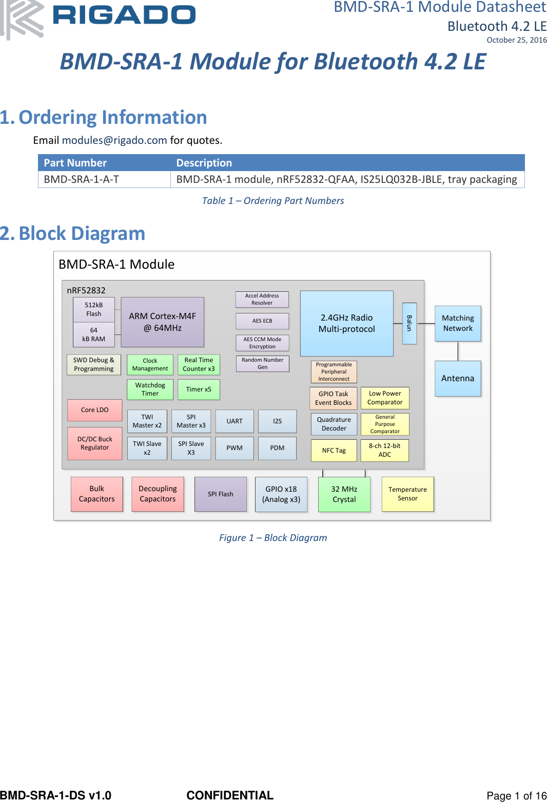
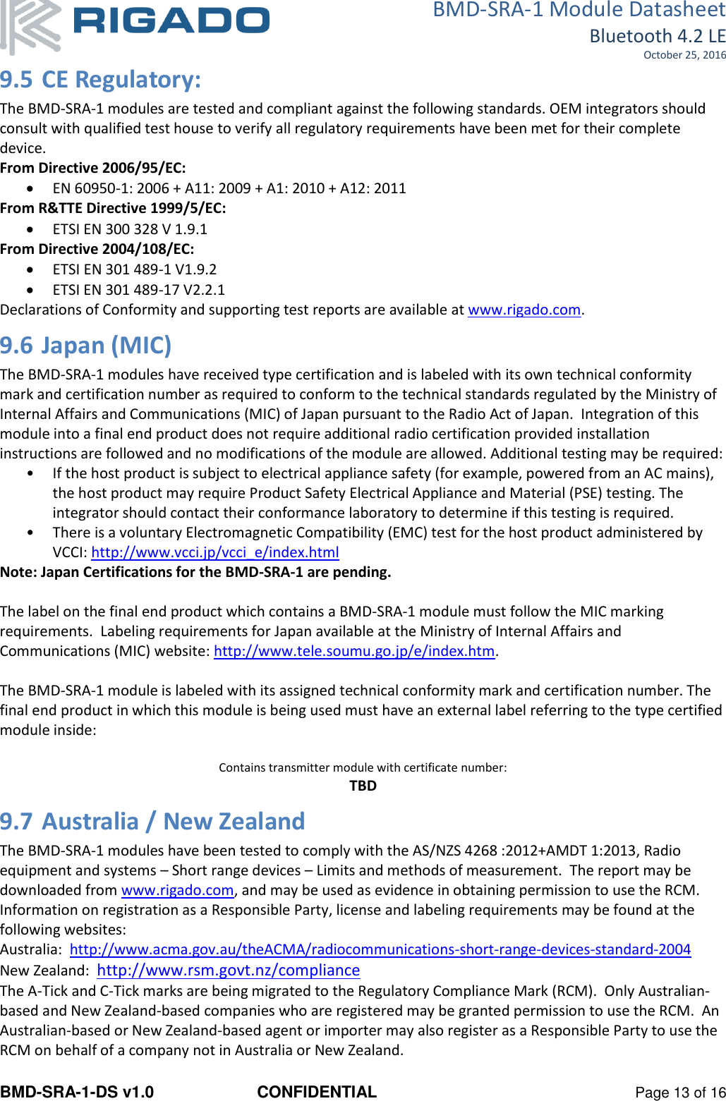
![BMD-SRA-1 Module Datasheet Bluetooth 4.2 LE October 25, 2016 BMD-SRA-1-DS v1.0 CONFIDENTIAL Page 4 of 16 4. Pin Descriptions 4.1 BMD-SRA-1 Figure 2 – BMD-SRA-1 Pin out Pin description Pin Name Direction Description A-1 P0.28 In/Out GPIO/AIN4 A-2 P0.31 In/Out GPIO/AIN7 A-3 P0.00 In/Out GPIO/XTAL1 (32.768kHz) A-8 P0.01 In/Out GPIO/XTAL2 (32.768kHz) A-9 P0.02 In/Out GPIO/AIN0 A-10 P0.03 In/Out GPIO/AIN1 A-12 P0.21 In/Out GPIO/RESET̅̅̅̅̅̅̅̅ A-18 P0.30 In/Out GPIO/AIN6 A-19 P0.29 In/Out GPIO/AIN5 A-20 P0.27 In/Out GPIO B-2 P0.12 In/Out GPIO B-4 P0.18 In/Out GPIO/TRACEDATA[0]/SWO B-5 P0.20 In/Out GPIO/TRACECLK B-8 P0.19 In/Out GPIO B-9 P0.17 In/Out GPIO/TRACEDATA[3] B-10 P0.16 In/Out GPIO/TRACEDATA[1] B-11 P0.11 In/Out GPIO B-12 P0.05 In/Out GPIO/AIN3 A-13 SWCLK In SWD Clock](https://usermanual.wiki/u-blox/06/User-Guide-3192404-Page-4.png)
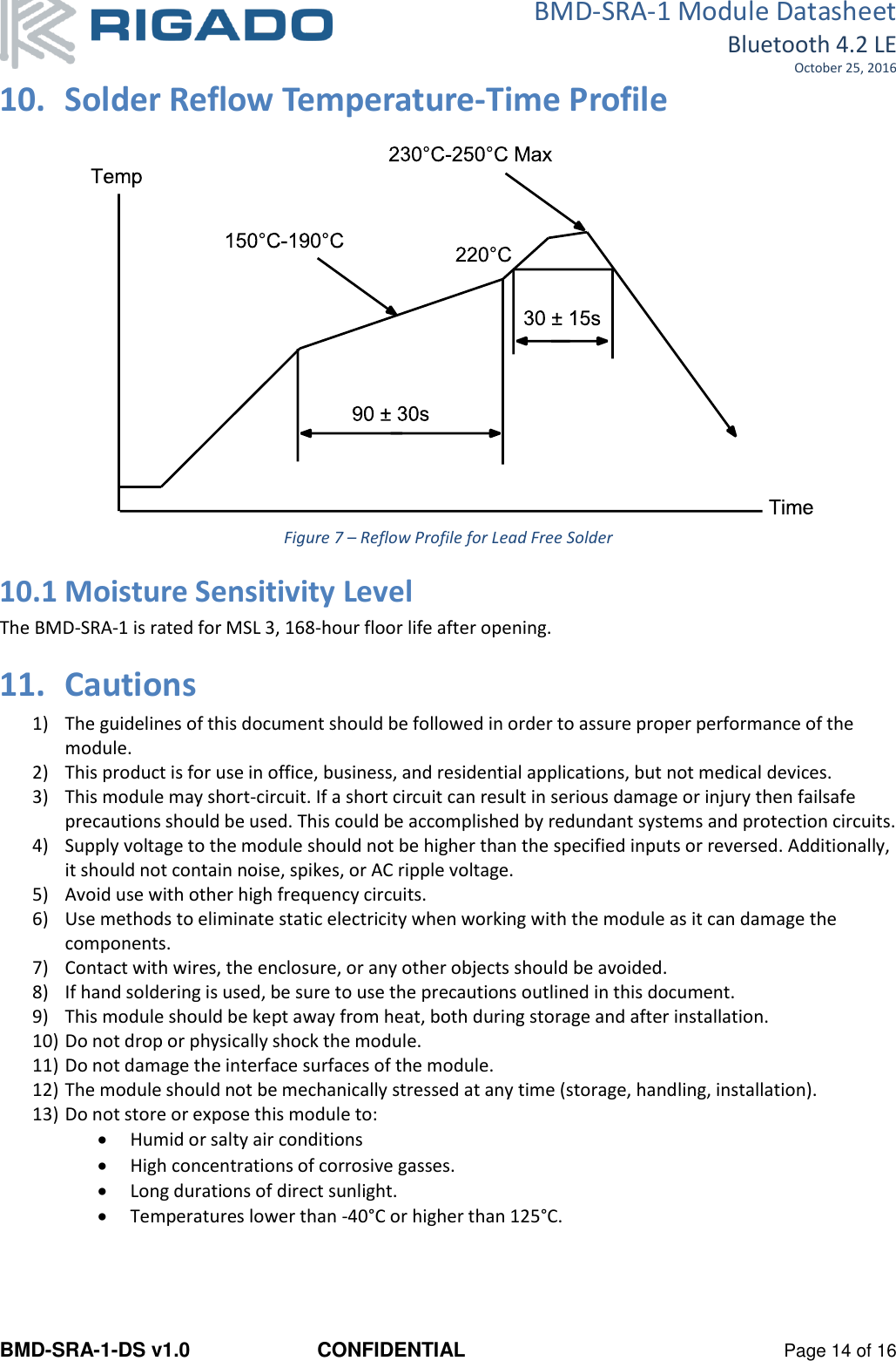
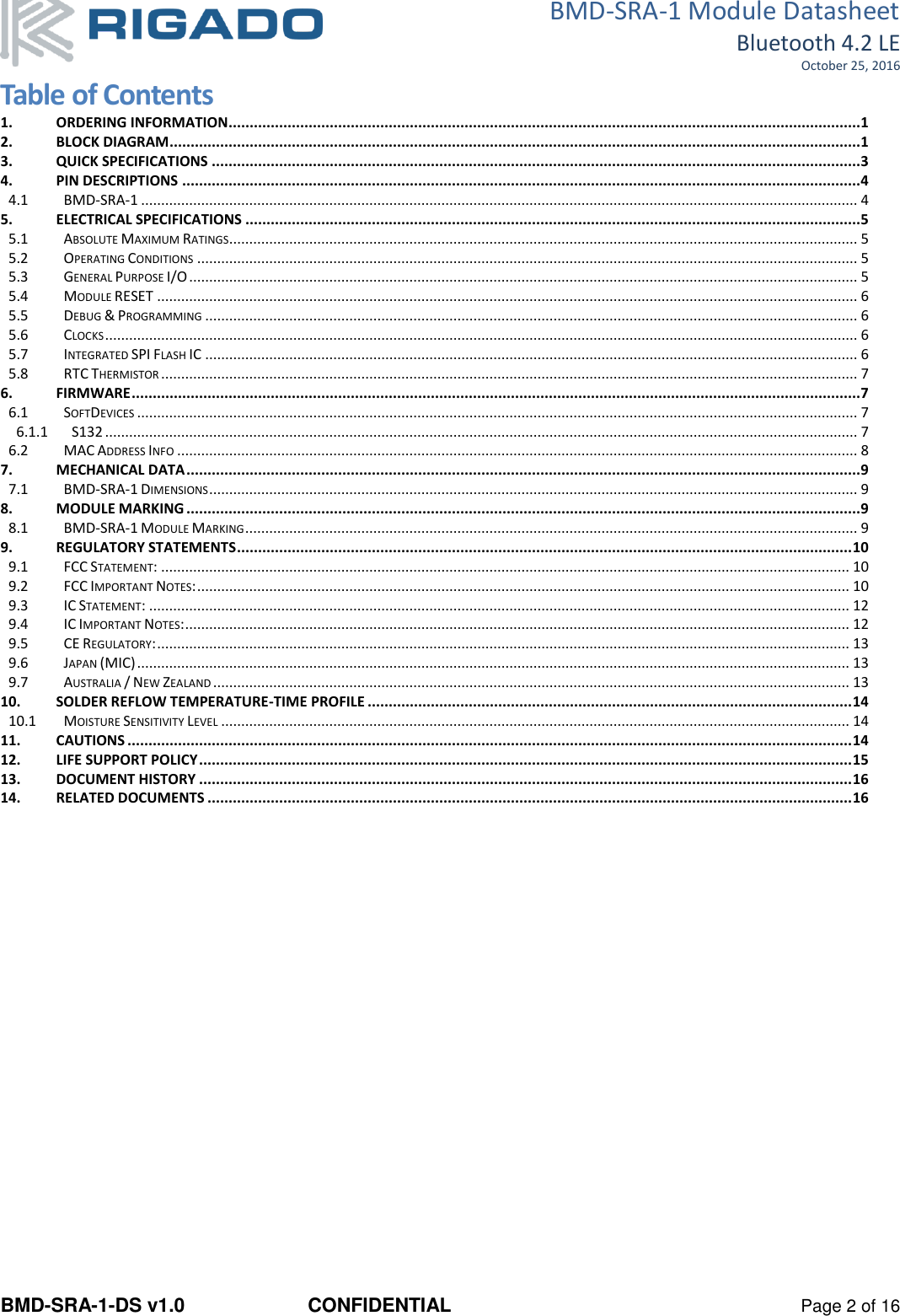
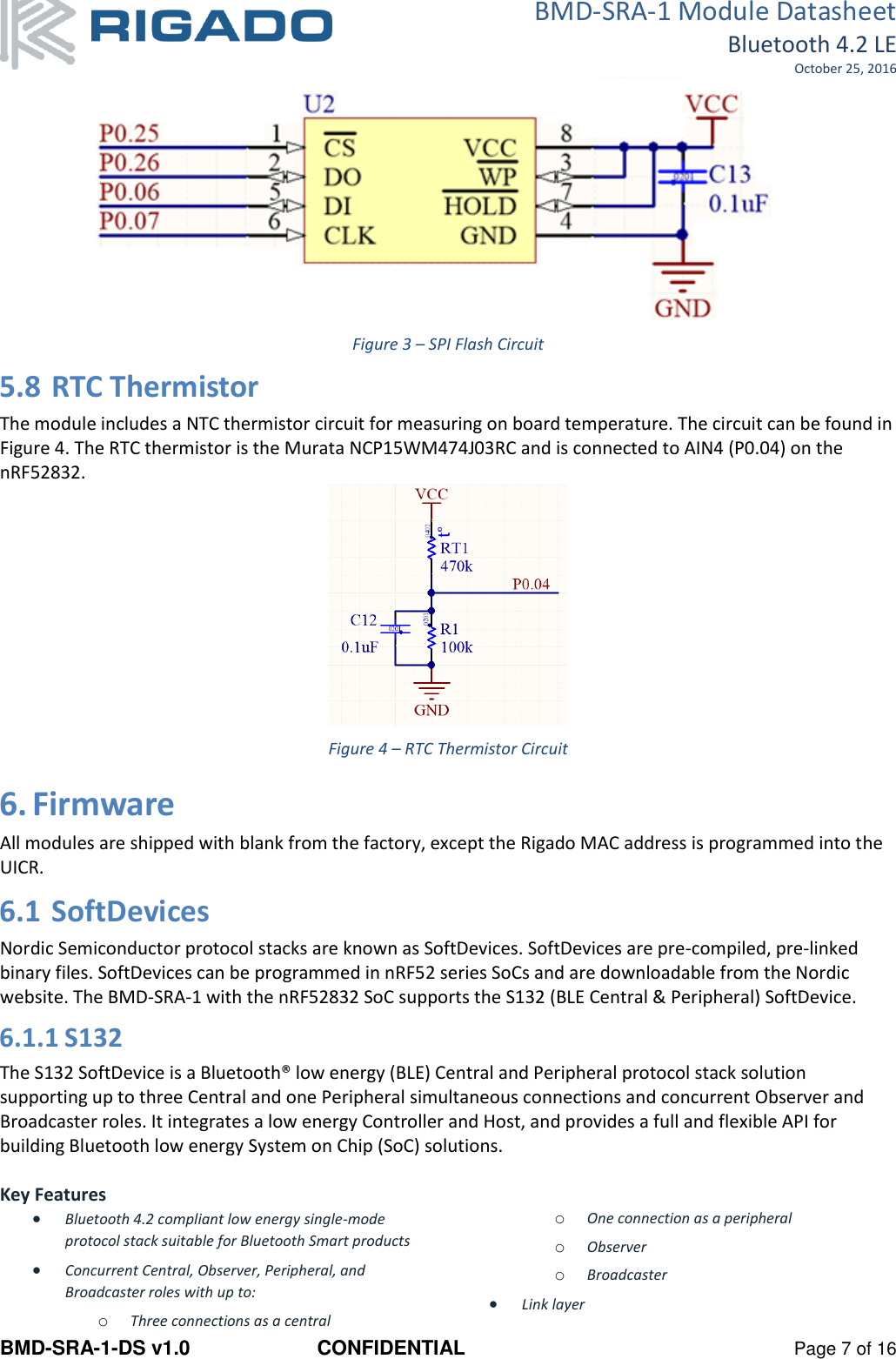
![BMD-SRA-1 Module Datasheet Bluetooth 4.2 LE October 25, 2016 BMD-SRA-1-DS v1.0 CONFIDENTIAL Page 6 of 16 RPU Pull-up Resistance 11 13 16 kΩ RPD Pull-down Resistance 11 13 16 kΩ Table 6 – GPIO 5.4 Module RESET GPIO pin P0.21 may be used for a hardware reset. In order to utilize P0.21 as a hardware reset, the UICR registers PSELRESET[0] and PSELRESET[1] must be set alike, to the value of 0x7FFFFF15. When P0.21 is programmed as RESET̅̅̅̅̅̅̅̅, the internal pull-up is automatically enabled. Rigado and Nordic example applications and development kits program P0.21 as RESET̅̅̅̅̅̅̅̅. 5.5 Debug & Programming The BMD-SRA-1 supports the two pin Serial Wire Debug (SWD) interface and offers flexible and powerful mechanism for non-intrusive debugging of program code. Breakpoints, single stepping, and instruction trace capture of code execution flow are part of this support. The BMD-SRA-1 also supports ETM and ITM trace. Trace data from the ETM and the ITM is sent to an external debugger via a 4-bit wide parallel trace port. In addition to parallel trace, the TPIU supports serial trace via the Serial Wire Output (SWO) trace protocol. 5.6 Clocks The BMD-SRA-1 utilizes two internal clock sources that are required for BLE operation. The high frequency clock is provided on-module by a high-accuracy 32-MHz crystal as required by the nRF52832 for radio operation. The low frequency clock is be provided internally by an RC oscillator or synthesized from the fast clock. Using the internal RC oscillator with calibration provides acceptable performance for BLE. Note: the ANT protocol requires the use of an external crystal. 32.768 kHz Oscillator Comparison Symbol Parameter Min. Typ. Max. Unit ILFXO Current for 32.768kHz Crystal Oscillator - 0.25 - µA ILFRC Current for 32.768kHz RC Oscillator - 0.6 1 µA ILFSYNT Current for 32.768kHz Synthesized Oscillator - 100 - µA fTOL_LFXO_BLE Frequency Tolerance, 32.768kHz Crystal Oscillator (BLE Stack)1 - - ±250 ppm fTOL_LFXO_ANT Frequency Tolerance, 32.768kHz Crystal Oscillator (ANT Stack)1 - - ±50 ppm f TOL_LFRC Frequency Tolerance, 32.768kHz RC Oscillator - - ±2 % fTOL_CAL_LFRC Frequency tolerance, 32.768kHz RC after calibration - - ±250 ppm fTOL_LFSYNT Frequency Tolerance, 32.768kHz Synthesized Oscillator - - ±48 ppm Note 1: fTOL_LFXO_BLE and fTOL_LFXO_ANT are the max allowed for BLE and ANT applications. Actual tolerance depends on the crystal used. Table 7 – 32.768 kHz Oscillator 5.7 Integrated SPI Flash IC All modules are shipped with blank from the factory, except the Rigado MAC address is programmed into the UICR.](https://usermanual.wiki/u-blox/06/User-Guide-3192404-Page-6.png)
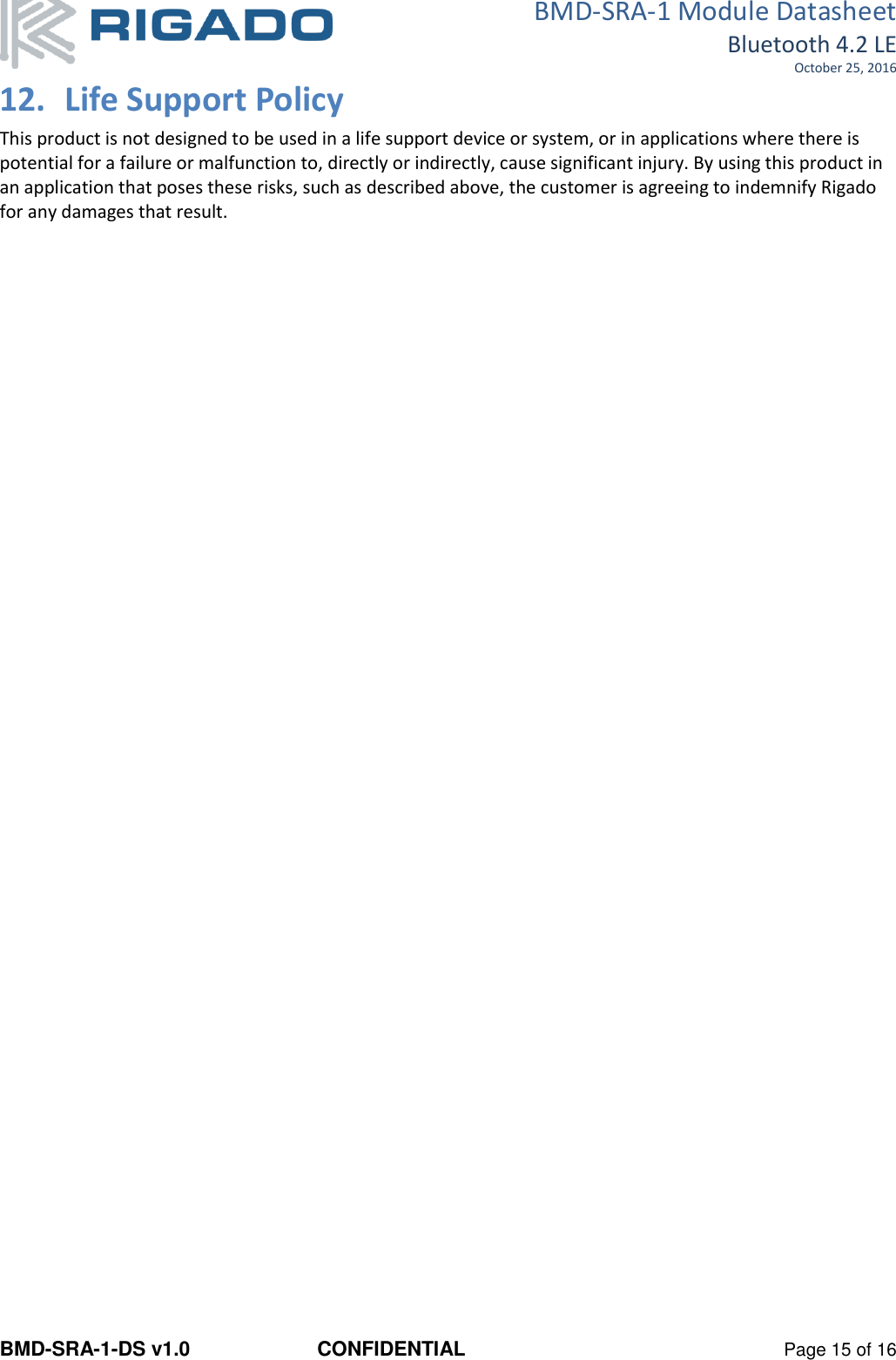
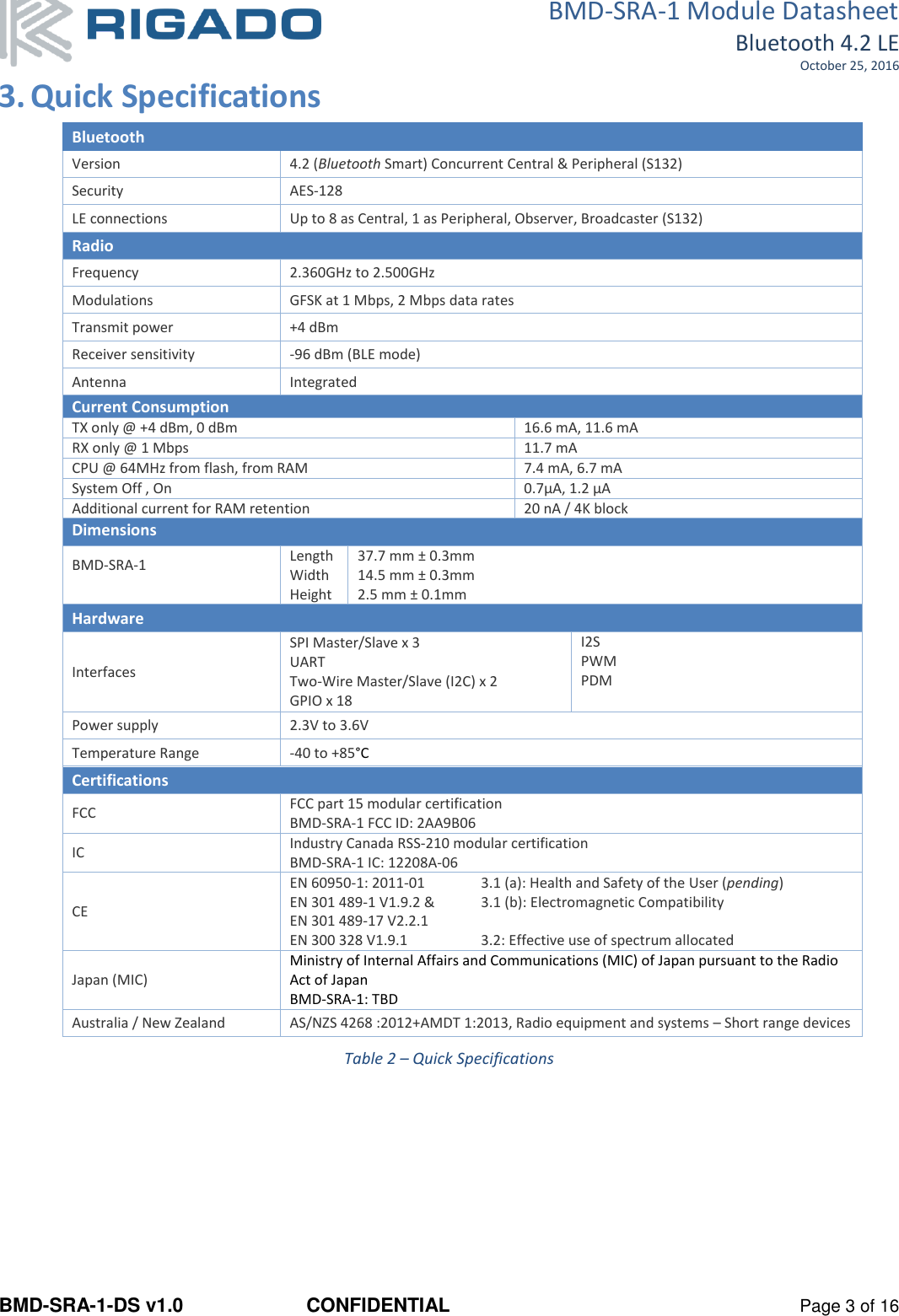
![BMD-SRA-1 Module Datasheet Bluetooth 4.2 LE October 25, 2016 BMD-SRA-1-DS v1.0 CONFIDENTIAL Page 8 of 16 L2CAP, ATT, and SM protocols GATT and GAP APIs GATT Client and Server Complementary nRF52 SDK including Bluetooth profiles and example applications Master Boot Record for over-the-air device firmware update Memory isolation between application and protocol stack for robustness and security Thread-safe supervisor-call based API Asynchronous, event-driven behavior No RTOS dependency o Any RTOS can be used No link-time dependencies o Standard ARM® CortexTMM4F project configuration for application development Support for concurrent and non-concurrent multiprotocol operation o Concurrent with the Bluetooth stack using concurrent multiprotocol timeslot API Alternate protocol stack in application space 6.2 MAC Address Info The BMD-SRA-1 modules comes preprogrammed with a unique MAC address from the factory. The MAC address is also printed on a 2D barcode on the top of the module. The 6-byte BLE Radio MAC address is stored in the nRF52832 UICR at NRF_UICR_BASE+0x80 LSB first. Please read the MAC Address Provisioning application note to avoid erasing/overwriting the MAC address during programming. UICR Register: NRF_UICR + 0x80 (0x10001080): MAC_Addr [0] (0xZZ) NRF_UICR + 0x81 (0x10001081): MAC_Addr [1] (0xYY) NRF_UICR + 0x82 (0x10001082): MAC_Addr [2] (0xXX) NRF_UICR + 0x83 (0x10001083): MAC_Addr [3] (0x93) NRF_UICR + 0x84 (0x10001084): MAC_Addr [4] (0x54) NRF_UICR + 0x85 (0x10001085): MAC_Addr [5] (0x94)](https://usermanual.wiki/u-blox/06/User-Guide-3192404-Page-8.png)