u blox 06 BMD-SRA-1 User Manual BMD SRA 1 Datasheet
Rigado LLC BMD-SRA-1 BMD SRA 1 Datasheet
u blox >
Users manual
BMD-SRA-1 Module Datasheet
Bluetooth 4.2 LE
October 25, 2016
BMD-SRA-1-DS v1.0 CONFIDENTIAL Page 1 of 16
BMD-SRA-1 Module for Bluetooth 4.2 LE
1. Ordering Information
Email modules@rigado.com for quotes.
Part Number
Description
BMD-SRA-1-A-T
BMD-SRA-1 module, nRF52832-QFAA, IS25LQ032B-JBLE, tray packaging
Table 1 – Ordering Part Numbers
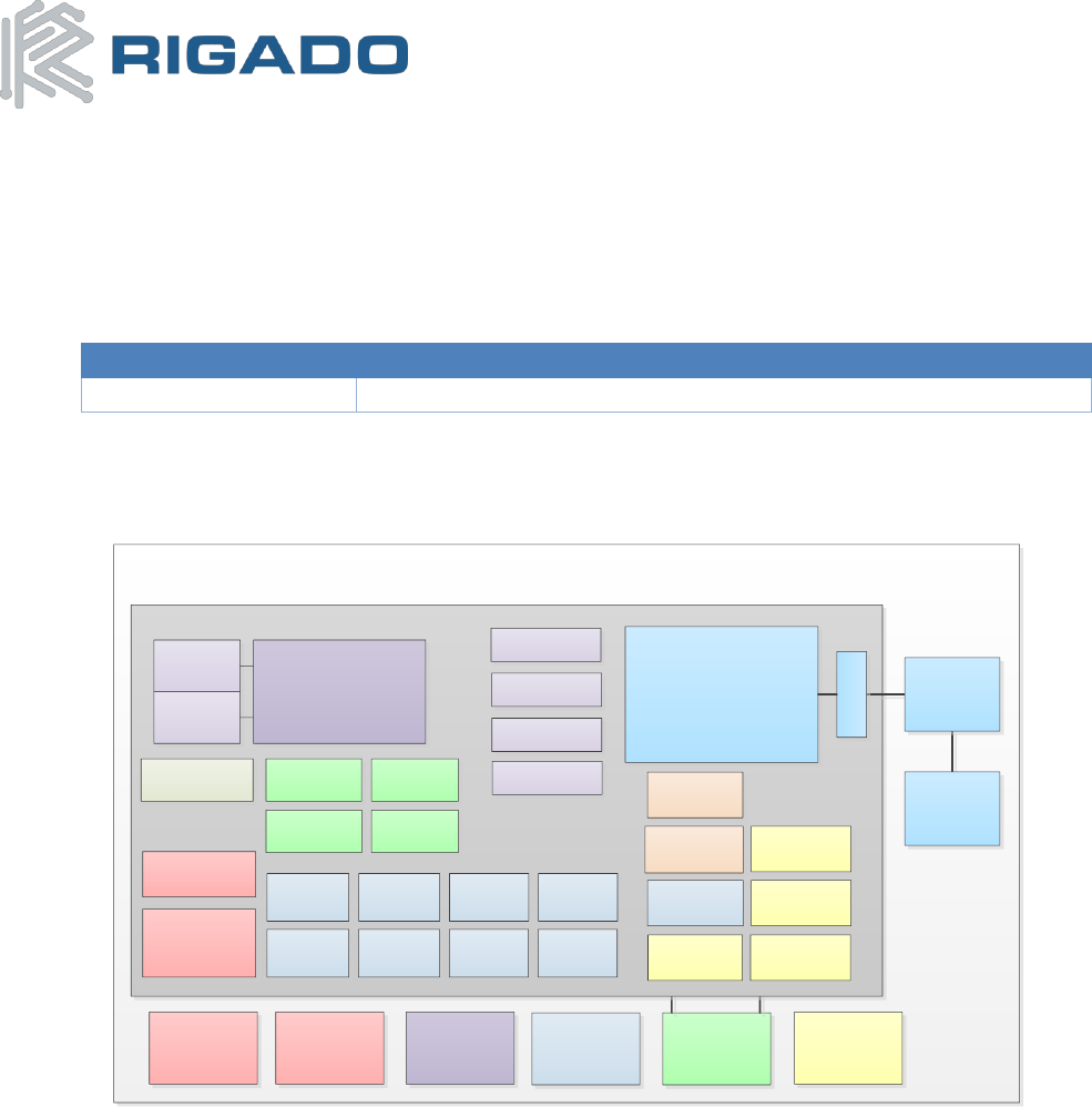
2. Block Diagram
BMD-SRA-1 Module
32 MHz
Crystal
nRF52832
512kB
Flash
Decoupling
Capacitors
Bulk
Capacitors
2.4GHz Radio
Multi-protocol
TWI
Master x2
SPI
Master x3
SPI Slave
X3
DC/DC Buck
Regulator
Core LDO
64
kB RAM
Low Power
Comparator
8-ch 12-bit
ADC
UART Quadrature
Decoder
SWD Debug &
Programming
Clock
Management
Watchdog
Timer
Random Number
Gen
Timer x5
Accel Address
Resolver
AES CCM Mode
Encryption
AES ECB
Real Time
Counter x3
GPIO Task
Event Blocks
Programmable
Peripheral
Interconnect
ARM Cortex-M4F
@ 64MHz Matching
Network
Antenna
GPIO x18
(Analog x3)
I2S
TWI Slave
x2 PWM PDM
General
Purpose
Comparator
NFC Tag
Balun
Temperature
Sensor
SPI Flash
Figure 1 – Block Diagram

BMD-SRA-1 Module Datasheet
Bluetooth 4.2 LE
October 25, 2016
BMD-SRA-1-DS v1.0 CONFIDENTIAL Page 2 of 16
Table of Contents
1. ORDERING INFORMATION...................................................................................................................................................... 1
2. BLOCK DIAGRAM .................................................................................................................................................................... 1
3. QUICK SPECIFICATIONS .......................................................................................................................................................... 3
4. PIN DESCRIPTIONS ................................................................................................................................................................. 4
4.1 BMD-SRA-1 ................................................................................................................................................................................... 4
5. ELECTRICAL SPECIFICATIONS .................................................................................................................................................. 5
5.1 ABSOLUTE MAXIMUM RATINGS............................................................................................................................................................. 5
5.2 OPERATING CONDITIONS ..................................................................................................................................................................... 5
5.3 GENERAL PURPOSE I/O ....................................................................................................................................................................... 5
5.4 MODULE RESET ............................................................................................................................................................................... 6
5.5 DEBUG & PROGRAMMING ................................................................................................................................................................... 6
5.6 CLOCKS ............................................................................................................................................................................................ 6
5.7 INTEGRATED SPI FLASH IC ................................................................................................................................................................... 6
5.8 RTC THERMISTOR .............................................................................................................................................................................. 7
6. FIRMWARE ............................................................................................................................................................................. 7
6.1 SOFTDEVICES .................................................................................................................................................................................... 7
6.1.1 S132 ............................................................................................................................................................................................ 7
6.2 MAC ADDRESS INFO .......................................................................................................................................................................... 8
7. MECHANICAL DATA ................................................................................................................................................................ 9
7.1 BMD-SRA-1 DIMENSIONS .................................................................................................................................................................. 9
8. MODULE MARKING ................................................................................................................................................................ 9
8.1 BMD-SRA-1 MODULE MARKING ......................................................................................................................................................... 9
9. REGULATORY STATEMENTS .................................................................................................................................................. 10
9.1 FCC STATEMENT: ............................................................................................................................................................................ 10
9.2 FCC IMPORTANT NOTES: ................................................................................................................................................................... 10
9.3 IC STATEMENT: ............................................................................................................................................................................... 12
9.4 IC IMPORTANT NOTES: ...................................................................................................................................................................... 12
9.5 CE REGULATORY: ............................................................................................................................................................................. 13
9.6 JAPAN (MIC) .................................................................................................................................................................................. 13
9.7 AUSTRALIA / NEW ZEALAND ............................................................................................................................................................... 13
10. SOLDER REFLOW TEMPERATURE-TIME PROFILE ................................................................................................................... 14
10.1 MOISTURE SENSITIVITY LEVEL ............................................................................................................................................................. 14
11. CAUTIONS ............................................................................................................................................................................ 14
12. LIFE SUPPORT POLICY ........................................................................................................................................................... 15
13. DOCUMENT HISTORY ........................................................................................................................................................... 16
14. RELATED DOCUMENTS ......................................................................................................................................................... 16

BMD-SRA-1 Module Datasheet
Bluetooth 4.2 LE
October 25, 2016
BMD-SRA-1-DS v1.0 CONFIDENTIAL Page 3 of 16
3. Quick Specifications
Bluetooth
Version
4.2 (Bluetooth Smart) Concurrent Central & Peripheral (S132)
Security
AES-128
LE connections
Up to 8 as Central, 1 as Peripheral, Observer, Broadcaster (S132)
Radio
Frequency
2.360GHz to 2.500GHz
Modulations
GFSK at 1 Mbps, 2 Mbps data rates
Transmit power
+4 dBm
Receiver sensitivity
-96 dBm (BLE mode)
Antenna
Integrated
Current Consumption
TX only @ +4 dBm, 0 dBm
16.6 mA, 11.6 mA
RX only @ 1 Mbps
11.7 mA
CPU @ 64MHz from flash, from RAM
7.4 mA, 6.7 mA
System Off , On
0.7µA, 1.2 µA
Additional current for RAM retention
20 nA / 4K block
Dimensions
BMD-SRA-1
Length
Width
Height
37.7 mm ± 0.3mm
14.5 mm ± 0.3mm
2.5 mm ± 0.1mm
Hardware
Interfaces
SPI Master/Slave x 3
UART
Two-Wire Master/Slave (I2C) x 2
GPIO x 18
I2S
PWM
PDM
Power supply
2.3V to 3.6V
Temperature Range
-40 to +85°C
Certifications
FCC
FCC part 15 modular certification
BMD-SRA-1 FCC ID: 2AA9B06
IC
Industry Canada RSS-210 modular certification
BMD-SRA-1 IC: 12208A-06
CE
EN 60950-1: 2011-01 3.1 (a): Health and Safety of the User (pending)
EN 301 489-1 V1.9.2 & 3.1 (b): Electromagnetic Compatibility
EN 301 489-17 V2.2.1
EN 300 328 V1.9.1 3.2: Effective use of spectrum allocated
Japan (MIC)
Ministry of Internal Affairs and Communications (MIC) of Japan pursuant to the Radio
Act of Japan
BMD-SRA-1: TBD
Australia / New Zealand
AS/NZS 4268 :2012+AMDT 1:2013, Radio equipment and systems – Short range devices
Table 2 – Quick Specifications
BMD-SRA-1 Module Datasheet
Bluetooth 4.2 LE
October 25, 2016
BMD-SRA-1-DS v1.0 CONFIDENTIAL Page 4 of 16
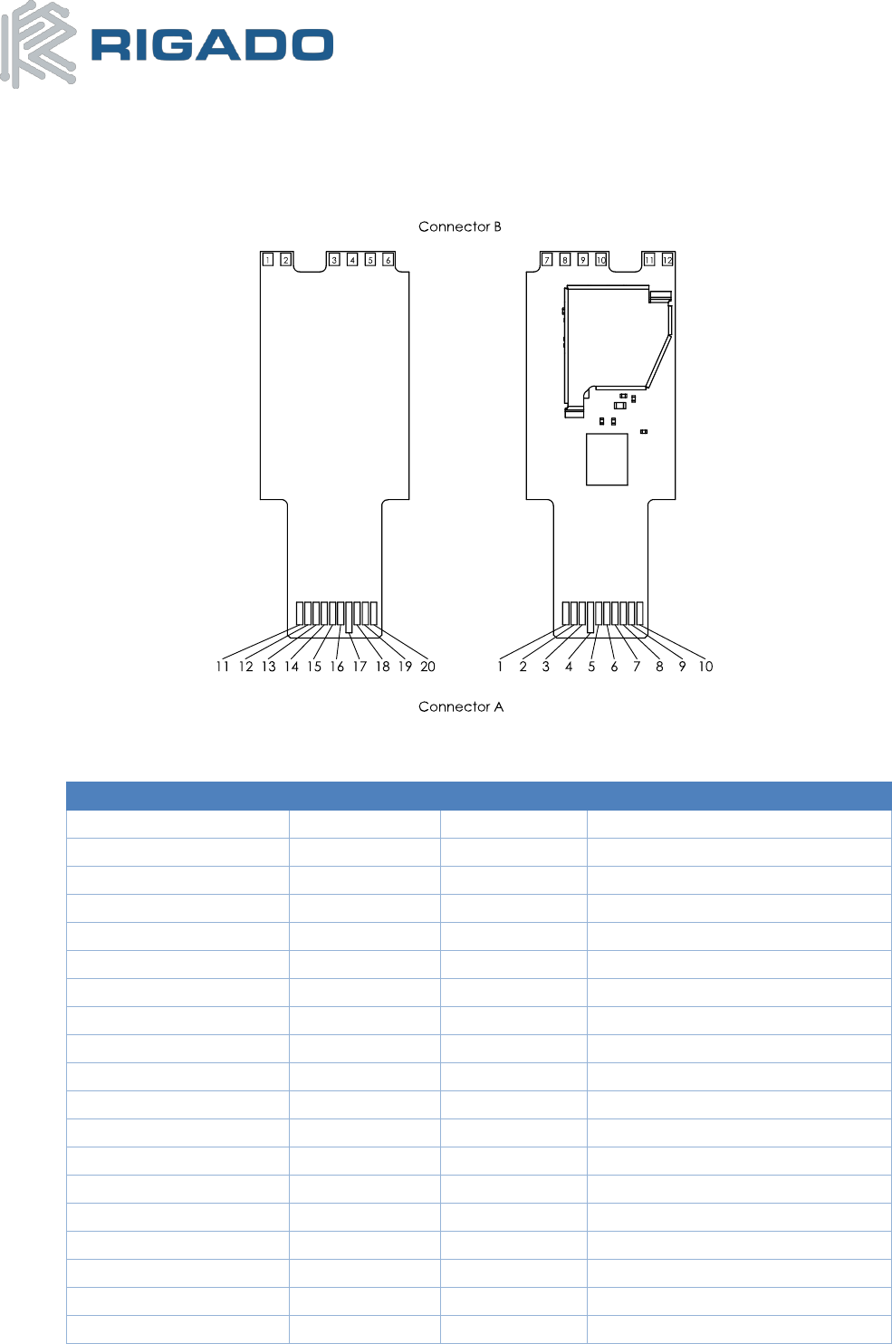
4. Pin Descriptions
4.1 BMD-SRA-1
Figure 2 – BMD-SRA-1 Pin out
Pin description
Pin
Name
Direction
Description
A-1
P0.28
In/Out
GPIO/AIN4
A-2
P0.31
In/Out
GPIO/AIN7
A-3
P0.00
In/Out
GPIO/XTAL1 (32.768kHz)
A-8
P0.01
In/Out
GPIO/XTAL2 (32.768kHz)
A-9
P0.02
In/Out
GPIO/AIN0
A-10
P0.03
In/Out
GPIO/AIN1
A-12
P0.21
In/Out
GPIO/RESET
̅
̅
̅
̅
̅
̅
̅
̅
A-18
P0.30
In/Out
GPIO/AIN6
A-19
P0.29
In/Out
GPIO/AIN5
A-20
P0.27
In/Out
GPIO
B-2
P0.12
In/Out
GPIO
B-4
P0.18
In/Out
GPIO/TRACEDATA[0]/SWO
B-5
P0.20
In/Out
GPIO/TRACECLK
B-8
P0.19
In/Out
GPIO
B-9
P0.17
In/Out
GPIO/TRACEDATA[3]
B-10
P0.16
In/Out
GPIO/TRACEDATA[1]
B-11
P0.11
In/Out
GPIO
B-12
P0.05
In/Out
GPIO/AIN3
A-13
SWCLK
In
SWD Clock

BMD-SRA-1 Module Datasheet
Bluetooth 4.2 LE
October 25, 2016
BMD-SRA-1-DS v1.0 CONFIDENTIAL Page 5 of 16
Pin
Name
Direction
Description
A-11
SWDIO
In/Out
SWD IO
A-17, B-6
VCC
Power
+2.3V to +3.6V
A-4, B-1, B-3, B-7
GND
Power
Electrical Ground
A-5, A-6, A-7, A-14, A-15,
A-16
NC
N/A
No Connect
Table 3 – BMD-SRA-1/301 Pin Descriptions
5. Electrical Specifications
5.1 Absolute Maximum Ratings
Symbol
Parameter
Min.
Max.
Unit
VCC_MAX
Voltage on supply pin
-0.3
3.9
V
VIO_MAX
Voltage on GPIO pins (VCC > 3.6V)
-0.3
3.9
V
VIO_MAX
Voltage on GPIO pins (VCC ≤ 3.6V)
-0.3
VCC + 0.3V
V
TS
Storage Temperature Range
-40
125
°C
Table 4 – Absolute Maximum Ratings
5.2 Operating Conditions
Symbol
Parameter
Min.
Typ.
Max.
Unit
VCC
Operating supply voltage
2.3
3.0
3.6
V
TR_VCC
Supply rise time (0V to 2.3V)
-
-
60
ms
TA
Operating Ambient Temperature Range
-40
25
85
°C
Table 5 – Operating Conditions
5.3 General Purpose I/O
The general purpose I/O is organized as one port enabling access and control of the 18 available GPIO pins through
one port. Each GPIO can be accessed individually with the following user configurable features:
Input/output direction
Output drive strength
Internal pull-up and pull-down resistors
Wake-up from high or low level triggers on all pins
Trigger interrupt on all pins
All pins can be used by the PPI task/event system; the maximum number of pins that can be interfaced
through the PPI at the same time is limited by the number of GPIOTE channels
All pins can be individually configured to carry serial interface or quadrature demodulator signals
Symbol
Parameter
Min.
Typ.
Max.
Unit
VIH
Input High Voltage
0.7 x VCC
-
VCC
V
VIL
Input Low Voltage
VSS
-
0.3 x VCC
V
VOH
Output High Voltage
VCC − 0.4
-
VCC
V
VOL
Output Low Voltage
VSS
-
VSS + 0.4
V

BMD-SRA-1 Module Datasheet
Bluetooth 4.2 LE
October 25, 2016
BMD-SRA-1-DS v1.0 CONFIDENTIAL Page 6 of 16
RPU
Pull-up Resistance
11
13
16
kΩ
RPD
Pull-down Resistance
11
13
16
kΩ
Table 6 – GPIO
5.4 Module RESET
GPIO pin P0.21 may be used for a hardware reset. In order to utilize P0.21 as a hardware reset, the UICR registers PSELRESET[0] and
PSELRESET[1] must be set alike, to the value of 0x7FFFFF15. When P0.21 is programmed as RESET
̅
̅
̅
̅
̅
̅
̅
̅
, the internal pull-up is automatically
enabled. Rigado and Nordic example applications and development kits program P0.21 as RESET
̅
̅
̅
̅
̅
̅
̅
̅
.
5.5 Debug & Programming
The BMD-SRA-1 supports the two pin Serial Wire Debug (SWD) interface and offers flexible and powerful
mechanism for non-intrusive debugging of program code. Breakpoints, single stepping, and instruction trace
capture of code execution flow are part of this support.
The BMD-SRA-1 also supports ETM and ITM trace. Trace data from the ETM and the ITM is sent to an external
debugger via a 4-bit wide parallel trace port. In addition to parallel trace, the TPIU supports serial trace via the
Serial Wire Output (SWO) trace protocol.
5.6 Clocks
The BMD-SRA-1 utilizes two internal clock sources that are required for BLE operation.
The high frequency clock is provided on-module by a high-accuracy 32-MHz crystal as required by the
nRF52832 for radio operation.
The low frequency clock is be provided internally by an RC oscillator or synthesized from the fast clock. Using
the internal RC oscillator with calibration provides acceptable performance for BLE. Note: the ANT protocol
requires the use of an external crystal.
32.768 kHz Oscillator Comparison
Symbol
Parameter
Min.
Typ.
Max.
Unit
ILFXO
Current for 32.768kHz Crystal Oscillator
-
0.25
-
µA
ILFRC
Current for 32.768kHz RC Oscillator
-
0.6
1
µA
ILFSYNT
Current for 32.768kHz Synthesized Oscillator
-
100
-
µA
fTOL_LFXO_BLE
Frequency Tolerance, 32.768kHz Crystal Oscillator
(BLE Stack)1
-
-
±250
ppm
fTOL_LFXO_ANT
Frequency Tolerance, 32.768kHz Crystal Oscillator
(ANT Stack)1
-
-
±50
ppm
f TOL_LFRC
Frequency Tolerance, 32.768kHz RC Oscillator
-
-
±2
%
fTOL_CAL_LFRC
Frequency tolerance, 32.768kHz RC after calibration
-
-
±250
ppm
fTOL_LFSYNT
Frequency Tolerance, 32.768kHz Synthesized
Oscillator
-
-
±48
ppm
Note 1: fTOL_LFXO_BLE and fTOL_LFXO_ANT are the max allowed for BLE and ANT applications. Actual tolerance depends
on the crystal used.
Table 7 – 32.768 kHz Oscillator
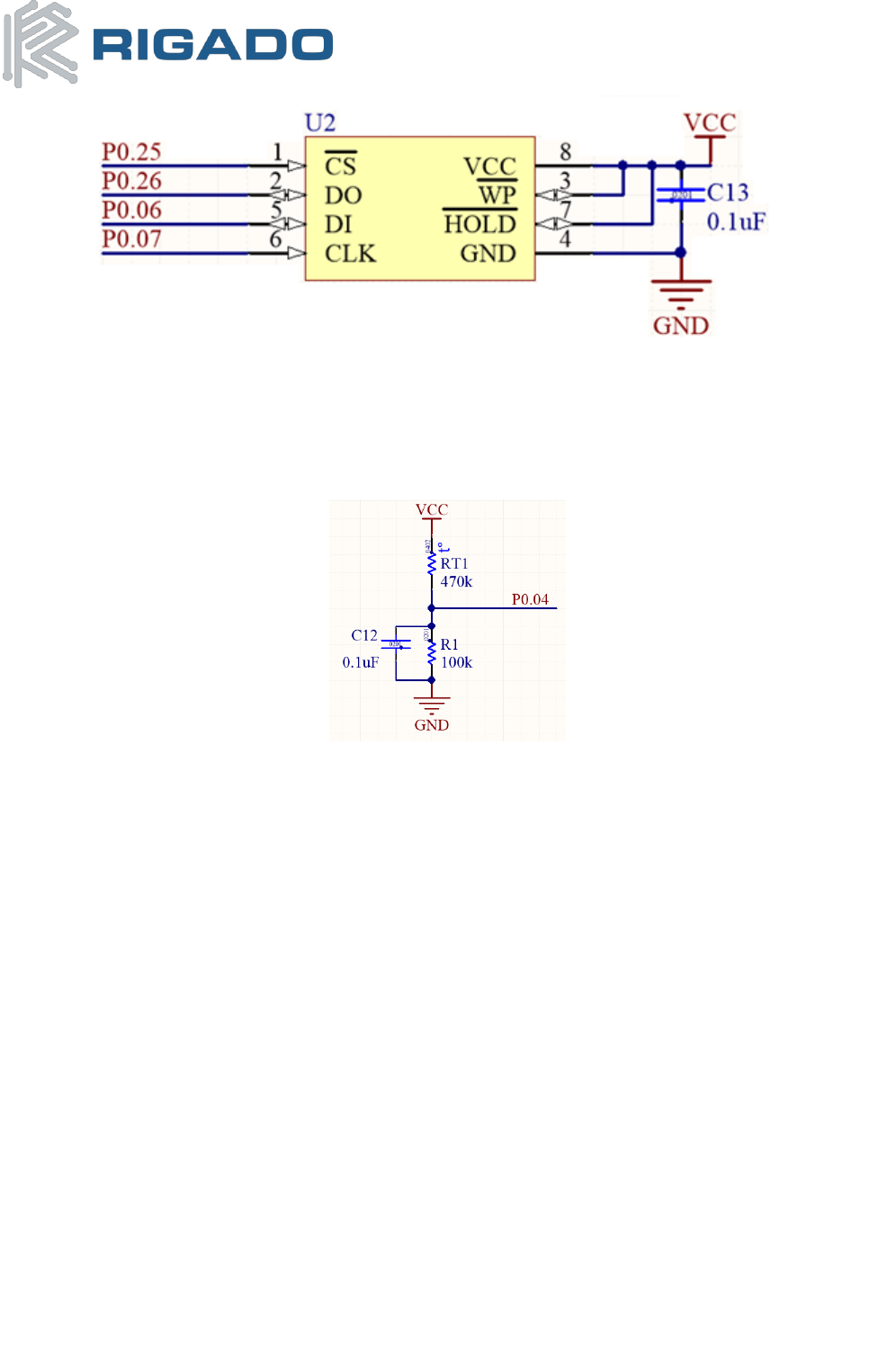
5.7 Integrated SPI Flash IC
All modules are shipped with blank from the factory, except the Rigado MAC address is programmed into the
UICR.
BMD-SRA-1 Module Datasheet
Bluetooth 4.2 LE
October 25, 2016
BMD-SRA-1-DS v1.0 CONFIDENTIAL Page 7 of 16
Figure 3 – SPI Flash Circuit
5.8 RTC Thermistor
The module includes a NTC thermistor circuit for measuring on board temperature. The circuit can be found in
Figure 4. The RTC thermistor is the Murata NCP15WM474J03RC and is connected to AIN4 (P0.04) on the
nRF52832.
Figure 4 – RTC Thermistor Circuit
6. Firmware
All modules are shipped with blank from the factory, except the Rigado MAC address is programmed into the
UICR.
6.1 SoftDevices
Nordic Semiconductor protocol stacks are known as SoftDevices. SoftDevices are pre-compiled, pre-linked
binary files. SoftDevices can be programmed in nRF52 series SoCs and are downloadable from the Nordic
website. The BMD-SRA-1 with the nRF52832 SoC supports the S132 (BLE Central & Peripheral) SoftDevice.
6.1.1 S132
The S132 SoftDevice is a Bluetooth® low energy (BLE) Central and Peripheral protocol stack solution
supporting up to three Central and one Peripheral simultaneous connections and concurrent Observer and
Broadcaster roles. It integrates a low energy Controller and Host, and provides a full and flexible API for
building Bluetooth low energy System on Chip (SoC) solutions.
Key Features
Bluetooth 4.2 compliant low energy single-mode
protocol stack suitable for Bluetooth Smart products
Concurrent Central, Observer, Peripheral, and
Broadcaster roles with up to:
o Three connections as a central
o One connection as a peripheral
o Observer
o Broadcaster
Link layer

BMD-SRA-1 Module Datasheet
Bluetooth 4.2 LE
October 25, 2016
BMD-SRA-1-DS v1.0 CONFIDENTIAL Page 8 of 16
L2CAP, ATT, and SM protocols
GATT and GAP APIs
GATT Client and Server
Complementary nRF52 SDK including Bluetooth profiles
and example applications
Master Boot Record for over-the-air device firmware
update
Memory isolation between application and protocol
stack for robustness and security
Thread-safe supervisor-call based API
Asynchronous, event-driven behavior
No RTOS dependency
o Any RTOS can be used
No link-time dependencies
o Standard ARM® CortexTMM4F project
configuration for application development
Support for concurrent and non-concurrent
multiprotocol operation
o Concurrent with the Bluetooth stack using
concurrent multiprotocol timeslot API
Alternate protocol stack in application space
6.2 MAC Address Info
The BMD-SRA-1 modules comes preprogrammed with a unique MAC address from the factory. The MAC
address is also printed on a 2D barcode on the top of the module.
The 6-byte BLE Radio MAC address is stored in the nRF52832 UICR at NRF_UICR_BASE+0x80 LSB first. Please
read the MAC Address Provisioning application note to avoid erasing/overwriting the MAC address during
programming.
UICR Register:
NRF_UICR + 0x80 (0x10001080): MAC_Addr [0] (0xZZ)
NRF_UICR + 0x81 (0x10001081): MAC_Addr [1] (0xYY)
NRF_UICR + 0x82 (0x10001082): MAC_Addr [2] (0xXX)
NRF_UICR + 0x83 (0x10001083): MAC_Addr [3] (0x93)
NRF_UICR + 0x84 (0x10001084): MAC_Addr [4] (0x54)
NRF_UICR + 0x85 (0x10001085): MAC_Addr [5] (0x94)
BMD-SRA-1 Module Datasheet
Bluetooth 4.2 LE
October 25, 2016
BMD-SRA-1-DS v1.0 CONFIDENTIAL Page 9 of 16
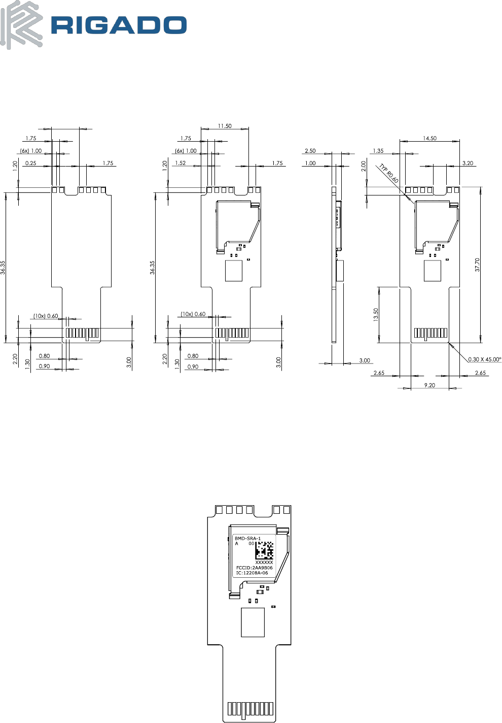
7. Mechanical Data
7.1 BMD-SRA-1 Dimensions
Figure 5 – BMD-SRA-1 Module Dimensions
(All dimensions are in mm)
8. Module Marking
8.1 BMD-SRA-1 Module Marking
Figure 6 – BMD-SRA-1 Module Marking – Rev A

BMD-SRA-1 Module Datasheet
Bluetooth 4.2 LE
October 25, 2016
BMD-SRA-1-DS v1.0 CONFIDENTIAL Page 10 of 16
9. Regulatory Statements
9.1 FCC Statement:
This device has been tested and found to comply with part 15 of the FCC rules. These limits are designed to
provide reasonable protection against harmful interference in a residential installation. This equipment
generates, uses and can radiate radio frequency energy and, if not installed and used in accordance with the
instructions, may cause harmful interference to radio communications. However, there is no guarantee that
interference will not occur in a particular installation. If this equipment does cause harmful interference to
radio or television reception, which can be determined by turning the equipment off and on, the user is
encouraged to try to correct the interference by one or more of the following measures:
Reorient or relocate the receiving antenna.
Increase the separation between the equipment and the receiver
Connect the equipment into an outlet on a circuit different from that to which the receiver is
connected.
Consult the dealer or an experienced radio/TV technician for help.
Operation is subjected to the following two conditions: (1) This device may no cause harmful interference, and
(2) this device must accept any interference received, including interference that may cause undesired
operation. Note: Modification to this product will void the user’s authority to operate this equipment.
Note: Modification to this product will void the users’ authority to operate this equipment.
9.2 FCC Important Notes:
(1) FCC Radiation Exposure Statement
This equipment complies with FCC RF radiation exposure limits set forth for an uncontrolled environment. This
transmitter must not be co-located or operating in conjunction with any other antenna or transmitter.
This equipment complies with Part 15 of the FCC Rules. Operation is subject the following two conditions:
(1) This device may not cause harmful interference, and
(2) This device must accept any interference received, including interference that may cause undesired
operation.
The devices must be installed and used in strict accordance with the manufacturer’s instructions as described
in this document.
Caution!
The manufacturer is not responsible for any radio or TV interference caused by unauthorized modifications to
this equipment. Such modification could void the user authority to operate the equipment.
(2) Co-location Warning:
This device and its antenna(s) must not be co-located or operating in conjunction with any other transmitter
antenna.
(3) OEM integration instructions:
This device is intended only for OEM integrators under the following conditions:
The antenna and transmitter must not be co-located with any other transmitter or antenna. The module shall
be only used with the integral antenna(s) that has been originally tested and certified with this module.
As long as the two (2) conditions above are met, further transmitter testing will not be required. However, the

BMD-SRA-1 Module Datasheet
Bluetooth 4.2 LE
October 25, 2016
BMD-SRA-1-DS v1.0 CONFIDENTIAL Page 11 of 16
OEM integrator is still responsible for testing their end-product for any additional compliance requirements
with this module installed (for example, digital device emission, PC peripheral requirements, etc.)
In the event that these conditions cannot be met (for example certain laptop configuration or co-location with
another transmitter), then the FCC authorization for this module in combination with the host equipment is
no longer considered valid and the FCC ID of the module cannot be used on the final product. In these and
circumstance, the OEM integrator will be responsible for re-evaluating. The end product (including the
transmitter) and obtaining a separate FCC authorization.
Caution!
The OEM is still responsible for verifying compliance with FCC Part 15, subpart B limits for unintentional
radiators through an accredited test facility.
(4) End product labeling:
The final end product must be labeled in a visible area with the following:
BMD-SRA-1: “Contains FCC ID: 2AA9B06”
Any similar wording that expresses the same meaning may be used.
The FCC Statement below should also be included on the label. When not possible, the FCC Statement should
be included in the User Manual of the host device.
“This device complies with part 15 of the FCC rules.
Operation is subject to the following two conditions. (1) This device may not cause harmful
interference. (2) This device must accept any interference received, including interference that may
cause undesired operation.”
(5) Information regarding the end user manual:
The OEM integrator has to be aware not to provide information to the end user regarding how to install or
remove this RF module in the user’s manual of the end product which integrates this module. The end user
manual shall include all required regulatory information/warning as show in this manual (Section 15.2(4)).

BMD-SRA-1 Module Datasheet
Bluetooth 4.2 LE
October 25, 2016
BMD-SRA-1-DS v1.0 CONFIDENTIAL Page 12 of 16
9.3 IC Statement:
This device complies with Industry Canada license-exempt RSS standard(s). Operation is subject to the
following two conditions: (1) this device may not cause interference, and (2) this device must accept any
interference, including interference that may cause undesired operation of the device.
Le présent appareil est conforme aux CNR d'Industrie Canada applicables aux appareils radio exempts de
licence. L'exploitation est autorisée aux deux conditions suivantes : (1) l'appareil ne doit pas produire de
brouillage, et (2) l'utilisateur de l'appareil doit accepter tout brouillage radioélectrique subi, même si le
brouillage est susceptible d'en compromettre le fonctionnement.
RF exposure warning: The equipment complies with RF exposure limits set forth for an uncontrolled
environment. The antenna(s) used for this transmitter must not be co-located or operating in conjunction with
any other antenna or transmitter.
Avertissement d'exposition RF: L'équipement est conforme aux limites d'exposition aux RF établies pour un
incontrôlés environnement. L'antenne (s) utilisée pour ce transmetteur ne doit pas être co-localisés ou
onctionner en conjonction avec toute autre antenne ou transmetteur .
9.4 IC Important Notes:
1. The OEM integrator has to be aware not to provide information to the end user regarding how to install or
remove this RF module in the user manual of the end product.
The user manual which is provided by OEM integrators for end users must include the following information in
a prominent location.
2. To comply with IC RF exposure compliance requirements, the antenna used for this transmitter must not be
co‐located or operating in conjunction with any other antenna or transmitter, except in accordance with IC
multi‐transmitter product procedures.
3. The final system integrator must ensure there is no instruction provided in the user manual or customer
documentation indicating how to install or remove the transmitter module except such device has
implemented two‐ways authentication between module and the host system.
4. The host device shall be properly labelled to identify the module within the host device. The final end
product must be labeled in a visible area with the following:
BMD-SRA-1: “Contains IC: 12208A-06“
Any similar wording that expresses the same meaning may be used.
The IC Statement below should also be included on the label. When not possible, the IC Statement should be
included in the User Manual of the host device.
“This device complies with Industry Canada license-exempt RSS standard(s). Operation is subject to
the following two conditions: (1) this device may not cause interference, and (2) this device must
accept any interference, including interference that may cause undesired operation of the device.
Le présent appareil est conforme aux CNR d'Industrie Canada applicables aux appareils radio exempts
de licence. L'exploitation est autorisée aux deux conditions suivantes : (1) l'appareil ne doit pas
produire de brouillage, et (2) l'utilisateur de l'appareil doit accepter tout brouillage radioélectrique
subi, même si le brouillage est susceptible d'en compromettre le onctionnement.”

BMD-SRA-1 Module Datasheet
Bluetooth 4.2 LE
October 25, 2016
BMD-SRA-1-DS v1.0 CONFIDENTIAL Page 13 of 16
9.5 CE Regulatory:
The BMD-SRA-1 modules are tested and compliant against the following standards. OEM integrators should
consult with qualified test house to verify all regulatory requirements have been met for their complete
device.
From Directive 2006/95/EC:
EN 60950-1: 2006 + A11: 2009 + A1: 2010 + A12: 2011
From R&TTE Directive 1999/5/EC:
ETSI EN 300 328 V 1.9.1
From Directive 2004/108/EC:
ETSI EN 301 489-1 V1.9.2
ETSI EN 301 489-17 V2.2.1
Declarations of Conformity and supporting test reports are available at www.rigado.com.
9.6 Japan (MIC)
The BMD-SRA-1 modules have received type certification and is labeled with its own technical conformity
mark and certification number as required to conform to the technical standards regulated by the Ministry of
Internal Affairs and Communications (MIC) of Japan pursuant to the Radio Act of Japan. Integration of this
module into a final end product does not require additional radio certification provided installation
instructions are followed and no modifications of the module are allowed. Additional testing may be required:
• If the host product is subject to electrical appliance safety (for example, powered from an AC mains),
the host product may require Product Safety Electrical Appliance and Material (PSE) testing. The
integrator should contact their conformance laboratory to determine if this testing is required.
• There is a voluntary Electromagnetic Compatibility (EMC) test for the host product administered by
VCCI: http://www.vcci.jp/vcci_e/index.html
Note: Japan Certifications for the BMD-SRA-1 are pending.
The label on the final end product which contains a BMD-SRA-1 module must follow the MIC marking
requirements. Labeling requirements for Japan available at the Ministry of Internal Affairs and
Communications (MIC) website: http://www.tele.soumu.go.jp/e/index.htm.
The BMD-SRA-1 module is labeled with its assigned technical conformity mark and certification number. The
final end product in which this module is being used must have an external label referring to the type certified
module inside:
Contains transmitter module with certificate number:
TBD
9.7 Australia / New Zealand
The BMD-SRA-1 modules have been tested to comply with the AS/NZS 4268 :2012+AMDT 1:2013, Radio
equipment and systems – Short range devices – Limits and methods of measurement. The report may be
downloaded from www.rigado.com, and may be used as evidence in obtaining permission to use the RCM.
Information on registration as a Responsible Party, license and labeling requirements may be found at the
following websites:
Australia: http://www.acma.gov.au/theACMA/radiocommunications-short-range-devices-standard-2004
New Zealand: http://www.rsm.govt.nz/compliance
The A-Tick and C-Tick marks are being migrated to the Regulatory Compliance Mark (RCM). Only Australian-
based and New Zealand-based companies who are registered may be granted permission to use the RCM. An
Australian-based or New Zealand-based agent or importer may also register as a Responsible Party to use the
RCM on behalf of a company not in Australia or New Zealand.
BMD-SRA-1 Module Datasheet
Bluetooth 4.2 LE
October 25, 2016
BMD-SRA-1-DS v1.0 CONFIDENTIAL Page 14 of 16
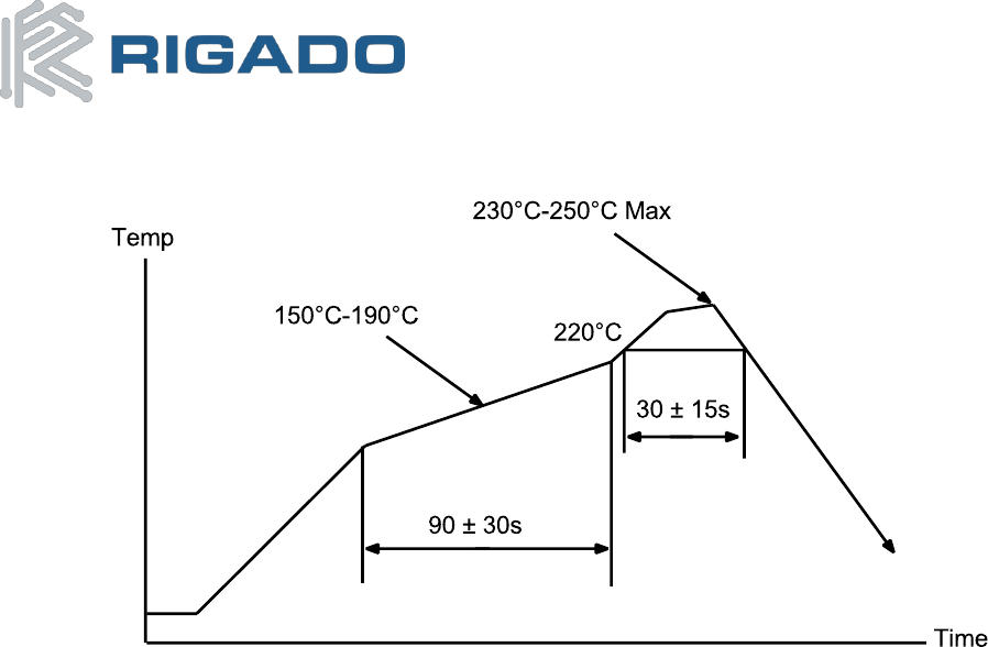
10. Solder Reflow Temperature-Time Profile
Figure 7 – Reflow Profile for Lead Free Solder
10.1 Moisture Sensitivity Level
The BMD-SRA-1 is rated for MSL 3, 168-hour floor life after opening.
11. Cautions
1) The guidelines of this document should be followed in order to assure proper performance of the
module.
2) This product is for use in office, business, and residential applications, but not medical devices.
3) This module may short-circuit. If a short circuit can result in serious damage or injury then failsafe
precautions should be used. This could be accomplished by redundant systems and protection circuits.
4) Supply voltage to the module should not be higher than the specified inputs or reversed. Additionally,
it should not contain noise, spikes, or AC ripple voltage.
5) Avoid use with other high frequency circuits.
6) Use methods to eliminate static electricity when working with the module as it can damage the
components.
7) Contact with wires, the enclosure, or any other objects should be avoided.
8) If hand soldering is used, be sure to use the precautions outlined in this document.
9) This module should be kept away from heat, both during storage and after installation.
10) Do not drop or physically shock the module.
11) Do not damage the interface surfaces of the module.
12) The module should not be mechanically stressed at any time (storage, handling, installation).
13) Do not store or expose this module to:
Humid or salty air conditions
High concentrations of corrosive gasses.
Long durations of direct sunlight.
Temperatures lower than -40°C or higher than 125°C.

BMD-SRA-1 Module Datasheet
Bluetooth 4.2 LE
October 25, 2016
BMD-SRA-1-DS v1.0 CONFIDENTIAL Page 15 of 16
12. Life Support Policy
This product is not designed to be used in a life support device or system, or in applications where there is
potential for a failure or malfunction to, directly or indirectly, cause significant injury. By using this product in
an application that poses these risks, such as described above, the customer is agreeing to indemnify Rigado
for any damages that result.
BMD-SRA-1 Module Datasheet
Bluetooth 4.2 LE
October 25, 2016
BMD-SRA-1-DS v1.0 CONFIDENTIAL Page 16 of 16
13. Document History
Revision
Date
Changes / Notes
0.8
9/22/2016
Initial preliminary release
0.9
9/29/2016
Updated mechanical drawing
1.0
10/25/2016
Updated certification status
14. Related Documents
Nordic Documents:
Visit infocenter.nordicsemi.com for a comprehensive library of Nordic technical documentation.
nRF52832 – nRF52832 Product Specification
S132-SDS – nRF52832 S132 Soft Device Specification