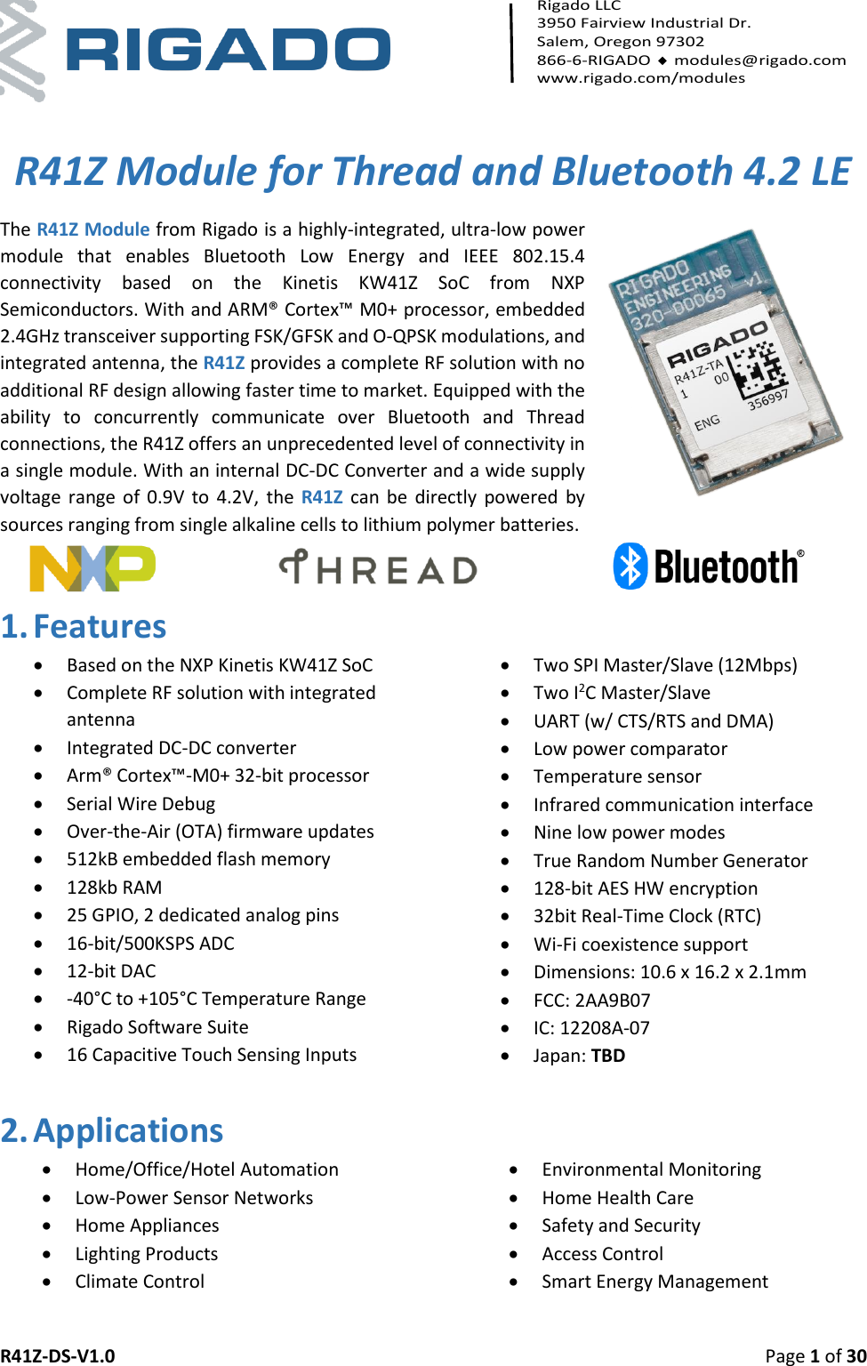
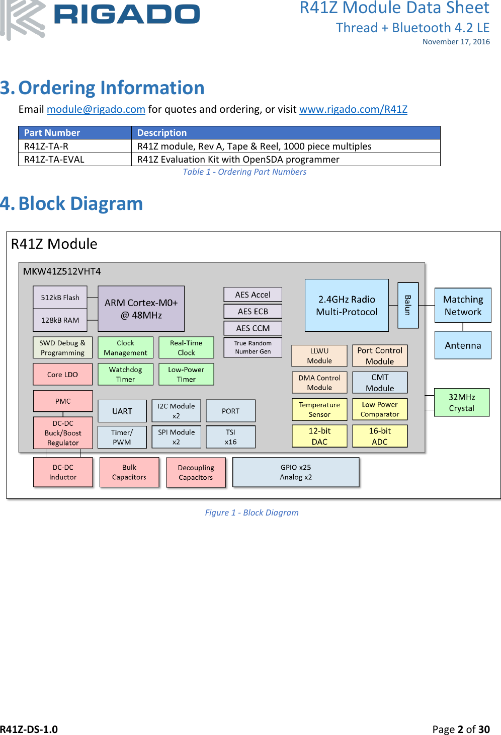
u blox 07 R41Z-T User Manual R41Z Data Sheet
Rigado LLC R41Z-T R41Z Data Sheet
UserManual.wiki
>
u blox
>
07 User Manual
Users manual
Navigation menu
Upload a User Manual
Namespaces
Wiki Guide
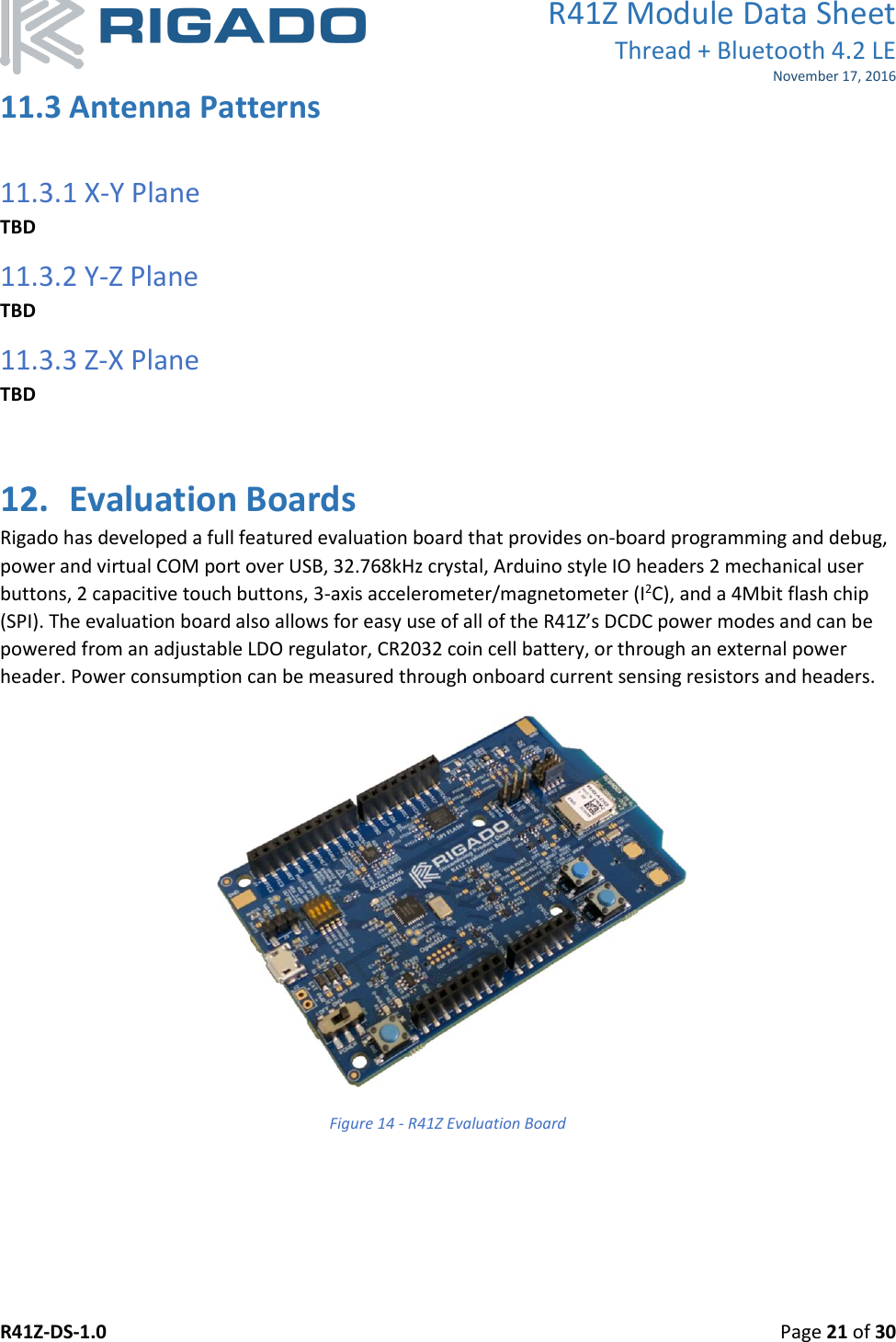
HTML
PDF
Info
Views
User Manual
Discussion / Help
Navigation