Users manual

R41Z-DS-V1.0 Page 1 of 30
Rigado LLC
3950 Fairview Industrial Dr.
Salem, Oregon 97302
866-6-RIGADO
modules@rigado.com
www.rigado.com/modules
R41Z Module for Thread and Bluetooth 4.2 LE
The R41Z Module from Rigado is a highly-integrated, ultra-low power
module that enables Bluetooth Low Energy and IEEE 802.15.4
connectivity based on the Kinetis KW41Z SoC from NXP
Semiconductors. With and ARM® Cortex™ M0+ processor, embedded
2.4GHz transceiver supporting FSK/GFSK and O-QPSK modulations, and
integrated antenna, the R41Z provides a complete RF solution with no
additional RF design allowing faster time to market. Equipped with the
ability to concurrently communicate over Bluetooth and Thread
connections, the R41Z offers an unprecedented level of connectivity in
a single module. With an internal DC-DC Converter and a wide supply
voltage range of 0.9V to 4.2V, the R41Z can be directly powered by
sources ranging from single alkaline cells to lithium polymer batteries.
1. Features
Based on the NXP Kinetis KW41Z SoC
Complete RF solution with integrated
antenna
Integrated DC-DC converter
Arm® Cortex™-M0+ 32-bit processor
Serial Wire Debug
Over-the-Air (OTA) firmware updates
512kB embedded flash memory
128kb RAM
25 GPIO, 2 dedicated analog pins
16-bit/500KSPS ADC
12-bit DAC
-40°C to +105°C Temperature Range
Rigado Software Suite
16 Capacitive Touch Sensing Inputs
Two SPI Master/Slave (12Mbps)
Two I2C Master/Slave
UART (w/ CTS/RTS and DMA)
Low power comparator
Temperature sensor
Infrared communication interface
Nine low power modes
True Random Number Generator
128-bit AES HW encryption
32bit Real-Time Clock (RTC)
Wi-Fi coexistence support
Dimensions: 10.6 x 16.2 x 2.1mm
FCC: 2AA9B07
IC: 12208A-07
Japan: TBD
2. Applications
Home/Office/Hotel Automation
Low-Power Sensor Networks
Home Appliances
Lighting Products
Climate Control
Environmental Monitoring
Home Health Care
Safety and Security
Access Control
Smart Energy Management
R41Z Module Data Sheet
Thread + Bluetooth 4.2 LE
November 17, 2016
R41Z-DS-1.0 Page 2 of 30
3. Ordering Information
Email module@rigado.com for quotes and ordering, or visit www.rigado.com/R41Z
Part Number
Description
R41Z-TA-R
R41Z module, Rev A, Tape & Reel, 1000 piece multiples
R41Z-TA-EVAL
R41Z Evaluation Kit with OpenSDA programmer
Table 1 - Ordering Part Numbers
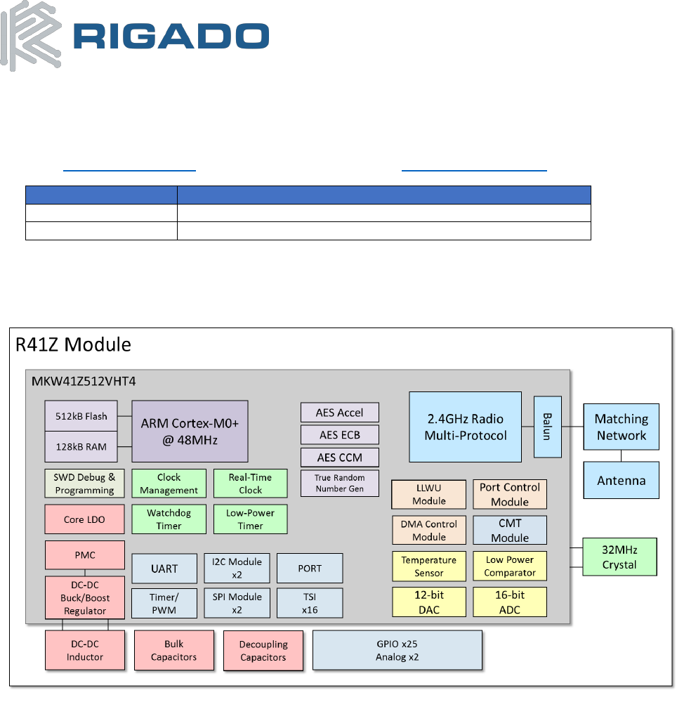
4. Block Diagram
Figure 1 - Block Diagram

R41Z Module Data Sheet
Thread + Bluetooth 4.2 LE
November 17, 2016
R41Z-DS-1.0 Page 3 of 30
Table of Contents
1. FEATURES .................................................................................................................................................. 1
2. APPLICATIONS ........................................................................................................................................... 1
3. ORDERING INFORMATION ......................................................................................................................... 2
4. BLOCK DIAGRAM ....................................................................................................................................... 2
5. QUICK SPECIFICATIONS .............................................................................................................................. 6
6. PIN DESCRIPTIONS ..................................................................................................................................... 7
6.1 R41Z PIN FUNCTIONS ........................................................................................................................................... 7
6.2 RIGDFU PIN FUNCTIONS ....................................................................................................................................... 8
7. ELECTRICAL SPECIFICATIONS ...................................................................................................................... 9
7.1 ABSOLUTE MAXIMUM RATINGS .............................................................................................................................. 9
7.2 OPERATING CONDITIONS ....................................................................................................................................... 9
7.3 DCDC CONVERTER OPERATION .............................................................................................................................. 9
7.3.1 DCDC BYPASS MODE ....................................................................................................................................... 10
7.3.2 DCDC BUCK MODE .......................................................................................................................................... 11
7.3.3 DCDC BOOST MODE ........................................................................................................................................ 12
7.4 GENERAL PURPOSE I/O AND PORTS ....................................................................................................................... 14
7.5 ANALOG I/O AND VREF ...................................................................................................................................... 15
7.5.1 ANALOG SIGNALS AND MAPPING ......................................................................................................................... 15
7.5.2 VDDA AND VREF ............................................................................................................................................ 15
7.6 MODULE RESET ................................................................................................................................................. 16
7.7 DEBUG AND PROGRAMMING ................................................................................................................................ 16
7.8 CLOCKS ............................................................................................................................................................ 16
8. FIRMWARE .............................................................................................................................................. 17
8.1 FACTORY IMAGE ................................................................................................................................................. 17
8.1.1 FIRMWARE VERSION ‘00’ ................................................................................................................................... 17
8.2 MAC ADDRESS INFO ........................................................................................................................................... 17
9. MECHANICAL DATA ................................................................................................................................. 18
9.1 PACKAGE DIMENSIONS ........................................................................................................................................ 18
9.2 RECOMMENDED PCB FOOTPRINT .......................................................................................................................... 19
10. MODULE MARKING ................................................................................................................................. 19
11. RF DESIGN NOTES .................................................................................................................................... 20
11.1 RECOMMENDED RF LAYOUT AND GROUND PLANE .................................................................................................... 20
11.2 MECHANICAL ENCLOSURE .................................................................................................................................... 20
11.3 ANTENNA PATTERNS ........................................................................................................................................... 21
11.3.1 X-Y PLANE ...................................................................................................................................................... 21
11.3.2 Y-Z PLANE ...................................................................................................................................................... 21
11.3.3 Z-X PLANE ...................................................................................................................................................... 21
12. EVALUATION BOARDS ............................................................................................................................. 21
13. CUSTOM DEVELOPMENT ......................................................................................................................... 22
14. BLUETOOTH QUALIFICATION ................................................................................................................... 22
15. REGULATORY STATEMENTS ..................................................................................................................... 22
15.1 FCC STATEMENT ................................................................................................................................................ 22
15.2 FCC IMPORTANT NOTES: ..................................................................................................................................... 23
15.3 IC STATEMENT: .................................................................................................................................................. 24
15.4 IC IMPORTANT NOTES: ........................................................................................................................................ 25
15.5 CE REGULATORY: ............................................................................................................................................... 25
15.6 JAPAN (MIC) .................................................................................................................................................... 26
15.7 AUSTRALIA / NEW ZEALAND ................................................................................................................................. 26
16. SOLDER REFLOW TEMPERATURE-TIME PROFILE ...................................................................................... 27
16.1 MOISTURE SENSITIVITY LEVEL ............................................................................................................................... 27

R41Z Module Data Sheet
Thread + Bluetooth 4.2 LE
November 17, 2016
R41Z-DS-1.0 Page 4 of 30
17. PACKAGING AND LABELING ..................................................................................................................... 28
17.1 CARRIER TAPE DIMENSION ................................................................................................................................... 28
17.2 REEL PACKAGING ............................................................................................................................................... 28
17.3 PACKAGING LABEL .............................................................................................................................................. 29
18. CAUTIONS ................................................................................................................................................ 29
19. LIFE SUPPORT POLICY .............................................................................................................................. 30
20. DOCUMENT HISTORY ............................................................................................................................... 30
21. RELATED DOCUMENTS ............................................................................................................................. 30

R41Z Module Data Sheet
Thread + Bluetooth 4.2 LE
November 17, 2016
R41Z-DS-1.0 Page 5 of 30
Table of Figures
FIGURE 1 - BLOCK DIAGRAM ............................................................................................................................... 2
FIGURE 2 - R41Z PIN OUT (TOP VIEW) ................................................................................................................. 7
FIGURE 3 - SCHEMATIC: DCDC BYPASS MODE EXAMPLE ....................................................................................... 10
FIGURE 4 - SCHEMATIC: DCDC BUCK MODE EXAMPLE .......................................................................................... 11
FIGURE 5 - SCHEMATIC: DCDC BUCK MODE PSWITCH EXAMPLE .......................................................................... 12
FIGURE 6 - SCHEMATIC: DCDC BOOST MODE EXAMPLE ........................................................................................ 13
FIGURE 7 - PCB: BOOST MODE SUGGESTED LAYOUT ............................................................................................ 14
FIGURE 8 - SCHEMATIC: LOW FREQUENCY CRYSTAL .............................................................................................. 17
FIGURE 9 - R41Z MAC ADDRESS ON LABEL ......................................................................................................... 18
FIGURE 10 - R41Z MODULE DIMENSIONS ........................................................................................................... 18
FIGURE 11 - R41Z PAD LAYOUT (TOP VIEW) ....................................................................................................... 19
FIGURE 12 - R41Z MODULE MARKING - ENG REV2 ............................................................................................. 19
FIGURE 13 - R41Z RF EXAMPLE BASED ON EVAL BOARD ...................................................................................... 20
FIGURE 14 - R41Z EVALUATION BOARD.............................................................................................................. 21
FIGURE 15 - REFLOW PROFILE FOR LEAD FREE SOLDER .......................................................................................... 27
FIGURE 16 - REEL CARTONS .............................................................................................................................. 28
FIGURE 17 - PACKAGING LABEL ......................................................................................................................... 29
Specification Tables
TABLE 1 - ORDERING PART NUMBERS ................................................................................................................... 2
TABLE 2 - QUICK SPECIFICATIONS ......................................................................................................................... 6
TABLE 3 - R41Z PIN DESCRIPTIONS ...................................................................................................................... 8
TABLE 4 - RIGDFU FUNCTIONS ............................................................................................................................ 8
TABLE 5 - ABSOLUTE MAXIMUM RATINGS ............................................................................................................. 9
TABLE 6 - OPERATING CONDITIONS ...................................................................................................................... 9
TABLE 7 - DCDC MODE CONNECTIONS ............................................................................................................... 10
TABLE 8 - DCDC BUCK MODE CONNECTIONS ...................................................................................................... 11
TABLE 9 - DCDC BOOST MODE CONNECTIONS .................................................................................................... 12
TABLE 10 - GPIO PROPERTIES ........................................................................................................................... 15
TABLE 11 - ANALOG SIGNALS ............................................................................................................................ 15
TABLE 12 - ANALOG PROPERTIES ....................................................................................................................... 16
TABLE 13 – LOW FREQUENCY CRYSTAL RECOMMENDED SPECIFICATIONS ................................................................. 16
R41Z Module Data Sheet
Thread + Bluetooth 4.2 LE
November 17, 2016
R41Z-DS-1.0 Page 6 of 30
5. Quick Specifications
Bluetooth
Version
4.2
Security
AES-128
LE Connections
2
Thread (IEEE 802.15.4)
Security
AES-128
Node Types
Router Eligible, End Device, REED
Radio
Frequency
2.360GHz to 2.483GHz
Modulations
GFSK @ 1Mbps, OQPSK @ 250kbps
Transmit power
+3.5dbm
Receiver sensitivity
-95dBm (BLE), -100dBm (IEEE 802.15.4)
Antenna
Integrated
Current Consumptions
TX only @ 0dBm, bypass mode
14.7 mA
TX only @ 0dBm, DCDC enabled, 3.6V Vin
6.1mA
RX only, bypass mode
16.2mA
RX only, DCDC enabled, 3.6V Vin
6.7mA
Normal Run CPU @ 48MHz @ 3.0V, DCDC enabled
4.8mA
Very-Low-Power Run CPU @ 4MHz @ 3.0V, DCDC enabled
137µA
Very-Low-Leakage Stop 3 (RAM retained) @ 3.0V @ 25°C, DCDC enabled
1.8 µA
Very-Low-Leakage Stop 0 @ 3.0V @25°C, bypass mode
182 nA
Dimensions
Length
Width
Height
16.2 mm ± 0.3mm
10.6 mm ± 0.3mm
2.1 mm ± 0.1mm
Hardware
Interfaces
SPI Master/Slave x2
UART x1
Touch Sense Interface x16
Two-Wire Mast/Slave (I2C) x2
GPIO x25
Analog input x6
Power Supply
Boost mode: 0.9V to 1.8V, 1.1V required at startup
Bypass mode: 1.71V to 3.6V
Buck mode: 1.8V to 4.2V, 2.1V required at startup
Temperature Range
-40 to +105 °C
Certifications
FCC
FCC part 15 modular certification ID: 2AA9B07
IC
Industry Canada RSS-210 modular certification IC: 12208A-07
CE
EN 60950-1: 2011-01 3.1 (a): Health and Safety of the User
EN 301 489-1 V1.9.2 & 3.1 (b): Electromagnetic Compatibility
EN 301 489-17 V2.2.1
EN 300 328 V1.9.1 3.2: Effective use of spectrum allocated
Japan (MIC)
Ministry of Internal Affairs and Communications (MIC) of Japan pursuant to the Radio Act
of Japan
Australia / New Zealand
AS/NZS 4268 :2012+AMDT 1:2013, Radio equipment and systems – Short range devices
Bluetooth
Pending
Thread
Pending
Table 2 - Quick Specifications
R41Z Module Data Sheet
Thread + Bluetooth 4.2 LE
November 17, 2016
R41Z-DS-1.0 Page 7 of 30
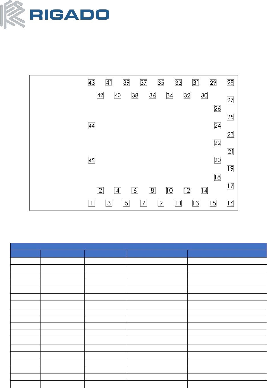
6. Pin Descriptions
6.1 R41Z Pin Functions
Figure 2 - R41Z Pin out (Top View)
GPIO/Analog
Pin
Name
Direction
Description
Default State at POR
2
PTC1
In/Out
GPIO
Disabled
3
PTC2
In/Out
GPIO
Disabled
4
PTC3
In/Out
GPIO
Disabled
5
PTC4
In/Out
GPIO
Disabled
6
PTC5
In/Out
GPIO
Disabled
7
PTC6
In/Out
GPIO
Disabled
8
PTC7
In/Out
GPIO
Disabled
10
PTC16
In/Out
GPIO
Disabled
11
PTC17
In/Out
GPIO
Disabled
12
PTC18
In/Out
GPIO
Disabled
13
PTC19
In/Out
GPIO
Disabled
14
PTA0
In/Out
GPIO
SWDIO, Pullup EN
15
PTA1
In/Out
GPIO
SWCLK, Pulldown EN
17
PTA2
In/Out
GPIO
Reset
̅
̅
̅
̅
̅
̅
̅
, Pullup EN
18
PTA16
In/Out
GPIO
Disabled
19
PTA17
In/Out
GPIO
Disabled
20
PTA18
In/Out
GPIO
Disabled
21
PTA19
In/Out
GPIO
Disabled
R41Z Module Data Sheet
Thread + Bluetooth 4.2 LE
November 17, 2016
R41Z-DS-1.0 Page 8 of 30
Pin
Name
Direction
Description
Default State at POR
30
PTB0
In/Out
GPIO
Disabled
31
PTB1
In/Out
GPIO
Disabled
32
PTB2
In/Out
GPIO
Disabled
33
PTB3
In/Out
GPIO
Disabled
34
PTB16
In/Out
GPIO
EXTAL32K
36
PTB17
In/Out
GPIO
XTAL23K
37
PTB18
In/Out
GPIO
Non Maskable Interrupt Req.
̅
̅
̅
̅
̅
̅
̅
̅
̅
̅
̅
̅
̅
̅
̅
̅
̅
̅
̅
̅
̅
̅
̅
̅
̅
̅
̅
̅
̅
̅
̅
̅
̅
̅
̅
̅
̅
38
ADC0_P
In
ADC/Comparator input
N/A
39
ADC0_N
In
ADC/Comparator input
N/A
Reference Signals
Pin
Name
Direction
Description
40
XTAL_OUT
Out
32MHz Clock output
41
VREF
In/Out
Analog reference voltage. Internally or externally sourced
42
VDDA
Power
Analog supply. Internally sourced1
Power
Pin
Name
Direction
Description
22
PSWITCH
Input
DCDC start signal2
23
DCDC_CFG
Input
DCDC mode2
25
VCC
Power
DCDC input2
26
DCDC_LP
Power
DCDC signal2
27
V1P8
Power
DCDC IO and peripheral voltage2
29
V1P5
Power
DCDC RF supply2
1, 9, 16,
24, 28,
35, 43,
44, 45
GND
Power
Electrical Ground
Note 1: VDDA is tied to V1P8 through a power filtering circuit on the R41Z module
Note 2: See the DCDC Converter Operation section for details on signal usage and DCDC modes
Table 3 - R41Z Pin Descriptions
6.2 RigDFU Pin Functions
When loaded with RigDFU, two GPIO pins are configured as UART pins for transferring new firmware
images to the R41Z. Pins are configured only when the bootloader is running and are fully available to
the application firmware. RigDFU can be removed from the R41Z by performing a full-chip erase.
Pin
Name
Direction
RigDFU Functions
7
PTC6
In
UART-RX for bootloader. Internal pulldown enabled.
8
PTC7
Out
UART-TX for bootloader. Hi-Z until bootloader activation message received on
UART RX
Table 4 - RigDFU Functions
R41Z Module Data Sheet
Thread + Bluetooth 4.2 LE
November 17, 2016
R41Z-DS-1.0 Page 9 of 30
7. Electrical Specifications
7.1 Absolute Maximum Ratings
Symbol
Parameter
Condition
Min.
Max.
Unit
Vcc_MAX
Voltage on Supply Pin
DCDC Boost Mode
-0.3
1.8
V
DCDC Bypass Mode
-0.3
3.6
V
DCDC Buck Mode
-0.3
4.2
V
V1P8_MAX
Voltage on V1P8 and GPIO
All DCDC modes
-0.3
3.6
V
VRF_MAX
Voltage on V1P5
All DCDC modes
-0.3
3.6
V
TS
Storage Temperature
-
-40
125
°C
Table 5 - Absolute Maximum Ratings
7.2 Operating Conditions
Symbol
Parameter
Condition
Min.
Typ.
Max.
Unit
Vcc
Voltage on Supply Pin
DCDC Boost Mode
0.91
1.5
1.8
V
DCDC Bypass Mode
1.71
3.3
3.6
V
DCDC Buck Mode
1.82
3.3
4.2
V
V1P8
Voltage on V1P8 and GPIO
All DCDC modes
1.45
3.3
3.6
V
VRF
Voltage on V1P5
All DCDC modes
1.8
3.3
3.6
V
I1P8
V1P8 output current
DCDC Buck Mode,
1.8Vout
-
-
45
mA
DCDC Buck Mode,
3.0Vout
-
-
27
mA
DCDC Boost Mode,
1.7Vin, 1.8 Vout
-
-
45
mA
DCDC Boost Mode,
0.9Vin, 3.0Vout
-
-
10
mA
TA
Ambient Temperature
-
-40
25
85
°C
Note 1: In Boost mode a minimum of 1.1V is required to start the DCDC converter. Once started, the
converter can operate at 0.9V
Note 2: In Buck mode a minimum of 2.1V is required to start the DCDC converter.
Table 6 - Operating Conditions
7.3 DCDC Converter Operation
The R41Z module contains an integrated DCDC converter which allows for three modes of operation
without additional components. When operating in DCDC Buck mode, power consumption from using
the radio can be reduced compared to DCDC Bypass mode. DCDC Boost mode allows the use of a single
alkaline or other low voltage source. While it is possible to switch between these modes in a single
design, for example the R41Z Evaluation Board, it is not recommended to switch between modes while
power is applied.
R41Z Module Data Sheet
Thread + Bluetooth 4.2 LE
November 17, 2016
R41Z-DS-1.0 Page 10 of 30
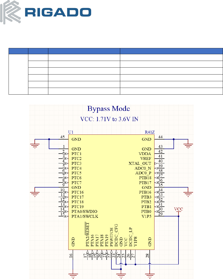
7.3.1 DCDC Bypass Mode
Mode
Pin
Name
Net Connection
Bypass
22
PSWITCH
Ground
23
DCDC_CFG
1.71V - 3.6V Source IN
25
VCC
1.71V - 3.6V Source IN
26
DCDC_LP
No Connection
27
V1P8
1.71V - 3.6V Source IN
29
V1P5
1.45V - 3.6V Source IN
Table 7 - DCDC Mode Connections
Figure 3 - Schematic: DCDC Bypass Mode Example
R41Z Module Data Sheet
Thread + Bluetooth 4.2 LE
November 17, 2016
R41Z-DS-1.0 Page 11 of 30
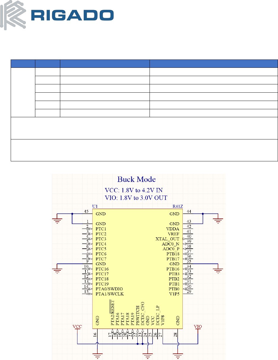
7.3.2 DCDC Buck Mode
Mode
Pin
Name
Net Connection
Buck
22
PSWITCH1
1.8V - 4.2V Source IN
23
DCDC_CFG
1.8V - 4.2V Source IN
25
VCC
1.8V - 4.2V Source IN
26
DCDC_LP
No Connection
27
V1P8
No Connection or 1.8V – 3.0V OUT2
29
V1P5
No Connection
Note 1: In Buck mode PSWITCH can inhibit the DCDC converter from starting when the source voltage is
applied. When PSWITCH is connected to the source voltage, the DCDC converter will start. Once started,
PSWITCH can be reconnected to GND without disrupting the DCDC converter’s operation.
Note 2: V1P8 is the R41Z’s IO voltage when the DCDC converter is running in either Buck or Boost mode.
V1P8 can source a limited number or additional peripheral devices (sensors, LEDs, etc.) that connect
directly to the R41Z’s IO. In Buck mode, V1P8 cannot output a voltage greater than the source voltage
Table 8 - DCDC Buck Mode Connections
Figure 4 - Schematic: DCDC Buck Mode Example
R41Z Module Data Sheet
Thread + Bluetooth 4.2 LE
November 17, 2016
R41Z-DS-1.0 Page 12 of 30
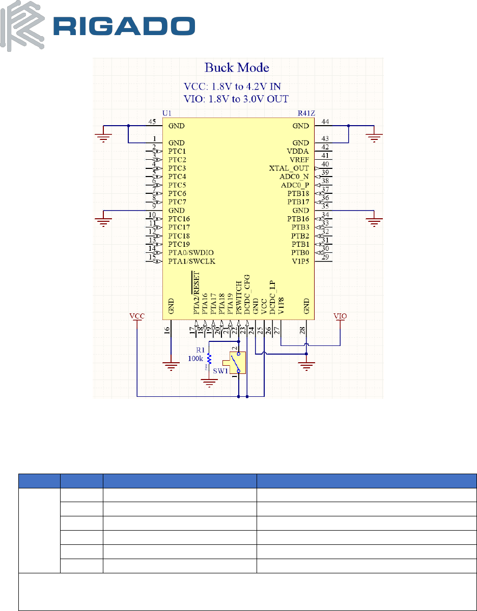
Figure 5 - Schematic: DCDC Buck Mode PSWITCH Example
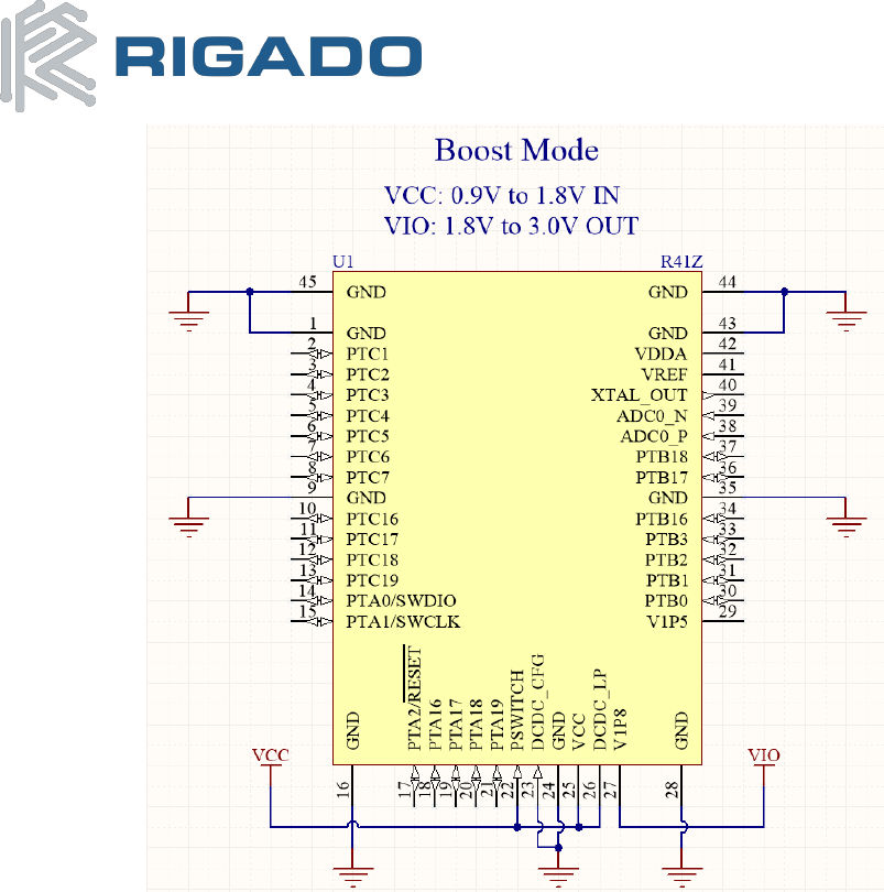
7.3.3 DCDC Boost Mode
Mode
Pin
Name
Net Connection
Boost
22
PSWITCH
0.9V – 1.8V Source IN
23
DCDC_CFG
Ground
25
VCC
0.9V – 1.8V Source IN
26
DCDC_LP
0.9V – 1.8V Source IN
27
V1P8
No Connection or 1.8V – 3.0V OUT1
29
V1P5
No Connection
Note 1: V1P8 is the R41Z’s IO voltage when the DCDC converter is running in either Buck or Boost mode.
V1P8 can source a limited number or additional peripheral devices (sensors, LEDs, etc.) that connect
directly to the R41Z’s IO.
Table 9 - DCDC Boost Mode Connections
R41Z Module Data Sheet
Thread + Bluetooth 4.2 LE
November 17, 2016
R41Z-DS-1.0 Page 13 of 30
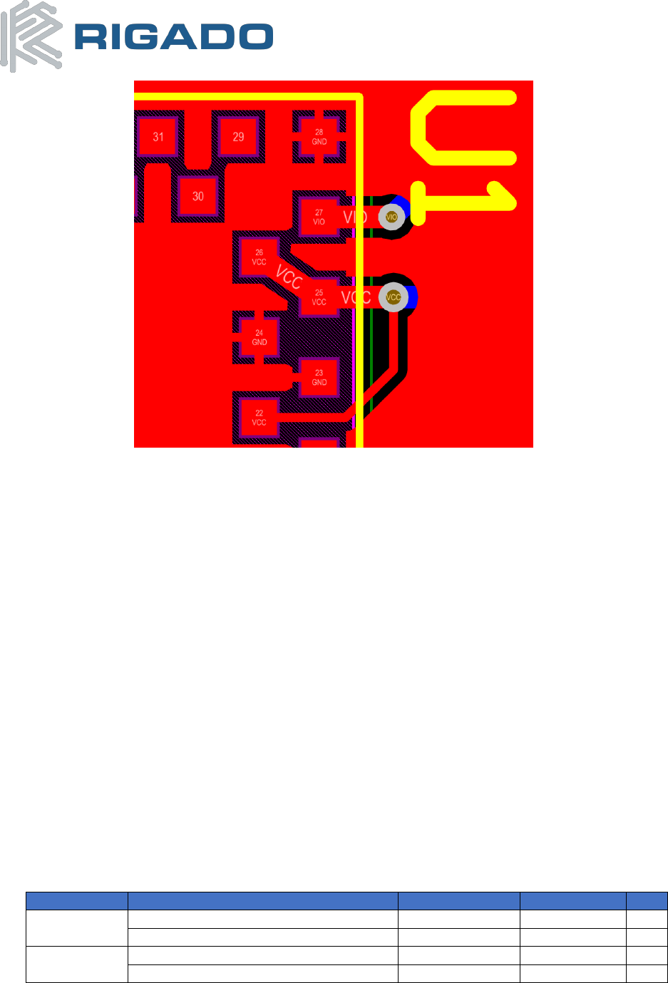
Figure 6 - Schematic: DCDC Boost Mode Example
When using Boost Mode care should be taken to ensure that DCDC_LP (Pin 26) is connected to VCC (Pin
25) with a trace wide enough to carry the full current expected to be drawn from the R41Z module and
any peripherals sourced by the module. The connection should also be as short as possible.
R41Z Module Data Sheet
Thread + Bluetooth 4.2 LE
November 17, 2016
R41Z-DS-1.0 Page 14 of 30
Figure 7 - PCB: Boost Mode Suggested Layout
7.4 General Purpose I/O and ports
The general purpose I/O is organized as three ports (A, B, and C) that enable access and control to each
of the 25 available GPIO pins. Each GPIO can be configured individually through a Pin Control Register
(PCR) and Port Data Direction Register (PDDR) with the following available features:
Input/Output direction
Output drive strength
Internal pull-up and pull-down resistors
Trigger interrupts and/or DMA from input
Read and clear interrupt flags
Enable passive input filter
Fast/slow slew rate selection
Control pin muxing to internal modules
To use a pin as GPIO set the Pin Mux Control field of the pin to ALT1 in the PCR. Ports must have their
clock source enabled in the System Clock Gating Control Register 5 (SIM_SCGC5) before accessing any
port registers. Attempting to access port registers without the port clock enabled will cause program
execution to immediately vector to the default exception handler. Disabling the clock to ports that are
not being used will reduce power consumption. Ports should be disabled before turning off the clock.
Symbol
Parameter
Min
Max.
Unit
VIH
Input High Voltage, 2.7V ≤ VIO ≤ 3.6V
0.7 × VIO
-
V
Input High Voltage, 1.7V ≤ VIO ≤ 2.7V
0.75 × VIO
-
V
VIL
Input Low Voltage, 2.7V ≤ VIO ≤ 3.6V
-
0.35 × VIO
V
Input Low Voltage, 1.7V ≤ VIO ≤ 2.7V
-
0.3 × VIO
V
DCDC_LP →
VCC →
PSWITCH →
DCDC_CFG →
V1P8 →
R41Z Module Data Sheet
Thread + Bluetooth 4.2 LE
November 17, 2016
R41Z-DS-1.0 Page 15 of 30
Symbol
Parameter
Min
Max.
Unit
VHYS
Input Hysteresis
-
0.06 × VIO
V
VOH
Output High Voltage
VIO – 0.5
-
V
VOL
Output Low Voltage
-
0.5
V
RP
Pull resistance
20
50
kΩ
Table 10 - GPIO Properties
7.5 Analog I/O and VREF
7.5.1 Analog Signals and Mapping
Analog ADC, DAC, and comparator signals can be routed to a select set of port or dedicated analog pins.
Generally, on port pins the analog function can be used by setting the Pin Mux Control field in the PCR of
the pin to ALT0.
Signal
Direction
Description
Pin
Port
Mux Alt
CMP0_OUT
Out
Comparator 0 Output
30
PTB0
ALT4
CMP0_IN0
In
Comparator 0 Single-ended input 0
38
-
-
CMP0_IN1
In
Comparator 0 Single-ended input 1
39
-
-
CMP0_IN2
In
Comparator 0 Single-ended input 2
37
PTB18
ALT0
CMP0_IN3
In
Comparator 0 Single-ended input 3
32
PTB2
ALT0
CMP0_IN4
In
Comparator 0 Single-ended input 4
33
PTB3
ALT0
CMP0_IN5
In
Comparator 0 Single-ended input 5
31
PTB1
ALT0
ADC0_SE0
In
ADC Channel 0 Single-ended input 0
31
PTB1
ALT0
ADC0_SE1
In
ADC Channel 0 Single-ended input 1
33
PTB3
ALT0
ADC0_SE2
In
ADC Channel 0 Single-ended input 2
32
PTB2
ALT0
ADC0_SE3
In
ADC Channel 0 Single-ended input 3
37
PTB18
ALT0
ADC0_SE4
In
ADC Channel 0 Single-ended input 4
21
PTA19
ALT0
ADC0_DP0
In
ADC Channel 0 Differential input positive
38
-
-
ADC0_DN0
In
ADC Channel 0 Differential input negative
39
-
-
DAC0_OUT
In
DAC Channel 0 Single-ended output
37
PTB18
ALT0
Table 11 - Analog Signals
7.5.2 VDDA and VREF
The source voltage for the analog sub-system, VDDA, is supplied by V1P8 through a filtering circuit
onboard the R41Z module. The voltage reference pin, VREF, has two sourcing options: internal and
external. When externally supplied, VREF should be referenced to VDDA. Internal sourcing is provided
by a resistor trimmed circuit. For details on using the analog modules, see the MKW41Z512 data sheet.
Symbol
Parameter
Min
Typ.
Max.
Unit
VDDA
Analog supply voltage
1.71
V1P8
V1P8
V
VREF_OUT
VREF internally sourced, factory trim
1.190
1.1950
1.200
V
VREFH
VREF externally sourced
1.13
VDDA
VDDA
V
VADIN
16-bit, differential mode
GND
-
31/32 × VREFH
V
16-bit, All other modes
GND
-
VREFH
V
VACIN
CMP/6-bit ADC analog input voltage
GND – 0.3
-
V1P8
V
VACIO
CMP/6-bit ADC analog input voltage offset
-
-
20
mV
ICMP
CMP current, High-speed mode
-
-
200
µA
R41Z Module Data Sheet
Thread + Bluetooth 4.2 LE
November 17, 2016
R41Z-DS-1.0 Page 16 of 30
Symbol
Parameter
Min
Typ.
Max.
Unit
CMP current, Low-speed mode
-
-
20
µA
VCMPH
Comparator output high
V1P8 – 0.5
-
-
V
VCMPL
Comparator output low
-
-
0.5
V
Table 12 - Analog Properties
7.6 Module Reset
Pin 17, PTA2, is used as an external reset source by default. This pin can be used for other functions,
such as GPIO, by setting the RESET_PIN_CFG option bit of the FTFA_FPORT register to 0. The setting of
this bit is retained through system resets and low power modes.
7.7 Debug and Programming
The R41Z module supports the two pin Serial Wire Debug (SWD) interface and offers flexible and
powerful mechanisms for non-intrusive debugging of program code. Breakpoints, single stepping, and
instruction trace capture of code execution flow are part of this support. The R41Z also supports Micro
Trace Buffer (MTB) which provides a lightweight program trace capabilities using system RAM. SWD pins
can be repurposed as additional GPIO by the application.
7.8 Clocks
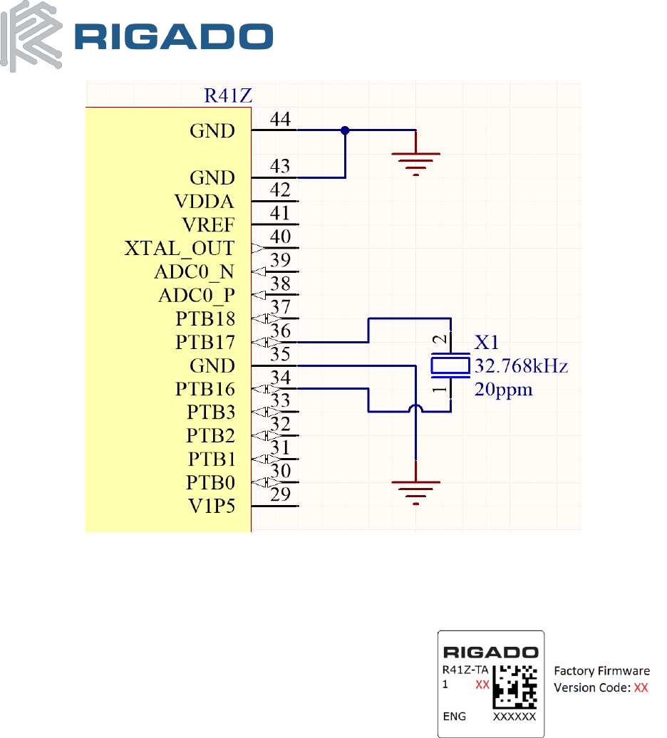
The R41Z requires two clocks: a high frequency clock and a low frequency clock.
The high frequency clock is provided on-module by a high accuracy 32-MHz crystal which is required for
Real Time Clock (RTC) and radio DeepSleep Mode (DSM) operation. In most applications, an external
crystal oscillator is required to provide the low frequency clock.
For normal run modes, an internal oscillator can provide the low frequency clock. However, to maintain
radio functionality in reduced power modes an external crystal must be used.
For most applications using the low frequency clock, external capacitors are not required. Internal,
programmable capacitors are provided on the R41Z module. In applications that use Rigado provided
firmware, use the typical specifications listed below.
An external clock source can be used in place of a crystal. In this case, the clock source should be
connected to the EXTAL32K pin (PTB16). XTAL23K (PTB17) should be left unconnected.
Low Frequency Crystal
Symbol
Parameter
Typ.
Max.
Unit
FNOM_LFXO
Crystal frequency
32.768
-
kHz
FTOL_LFXO_BLE
Frequency tolerance, BLE applications
±20
±250
ppm
CL_LFXO
Load Capacitance
7
12.5
pF
Table 13 – Low Frequency Crystal Recommended Specifications
R41Z Module Data Sheet
Thread + Bluetooth 4.2 LE
November 17, 2016
R41Z-DS-1.0 Page 17 of 30
Figure 8 - Schematic: Low Frequency Crystal
8. Firmware
8.1 Factory Image
All modules are shipped with factory programmed firmware. The
factory programmed firmware version is indicated on the label.
8.1.1 Firmware Version ‘00’
R41Z modules marked with firmware version ‘00’ are not loaded with a firmware image at the factory.
Note: when the R41Z does not have a firmware image loaded that can be executed out of POR, the R41Z
module will re-assert POR.
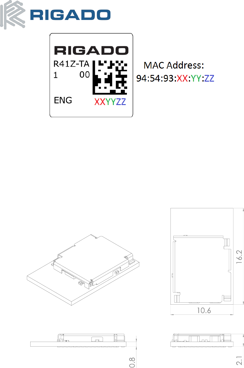
8.2 Mac Address Info
On R41Z modules, the MAC address is typically located in flash as part of the firmware image and is
typically accessed as a global constant. Rigado provides a unique MAC address which may be used in an
end application. The MAC address is printed on a 2D barcode and human readable text on the top of the
module.
R41Z Module Data Sheet
Thread + Bluetooth 4.2 LE
November 17, 2016
R41Z-DS-1.0 Page 18 of 30
Figure 9 - R41Z MAC Address on Label
When loading custom firmware to the module, the MAC address must be inserted into the image. This
can be done manually using the human readable text or automated using a barcode scanner and
suitable factory programmer tools. When loading a new application to the module care should be taken
to ensure the Rigado bootloader (if used) and MAC address are not overwritten.
9. Mechanical Data
9.1 Package Dimensions
Figure 10 - R41Z Module Dimensions
(All dimensions are in mm)
R41Z Module Data Sheet
Thread + Bluetooth 4.2 LE
November 17, 2016
R41Z-DS-1.0 Page 19 of 30
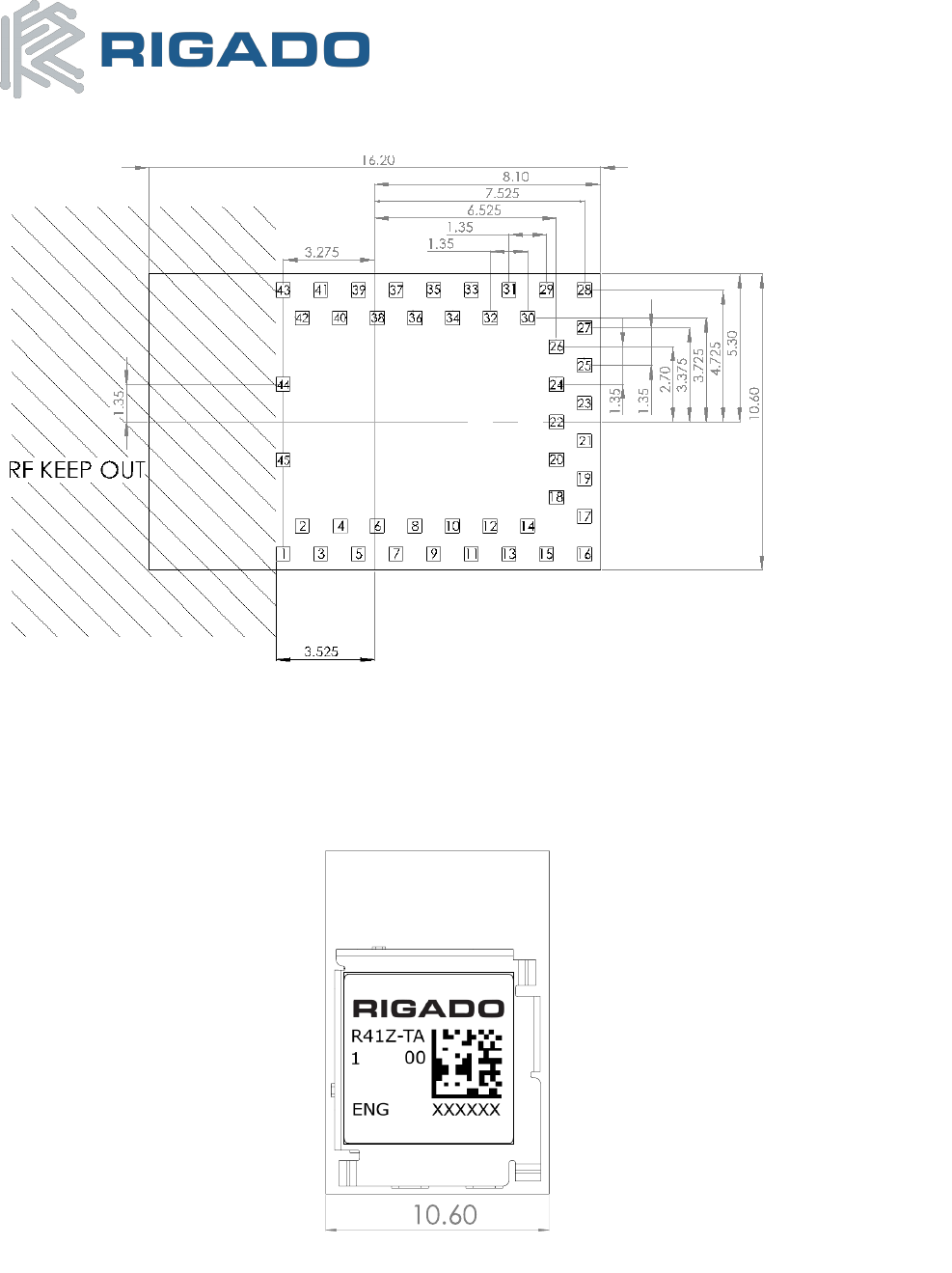
9.2 Recommended PCB Footprint
Figure 11 - R41Z Pad Layout (Top View)
(All dimensions are in mm)
10. Module Marking
PAD DIMENSIONS: 0.60MM X 0.60MM
RIGADO
320-00065 v2
Figure 12 - R41Z Module Marking - ENG Rev2
R41Z Module Data Sheet
Thread + Bluetooth 4.2 LE
November 17, 2016
R41Z-DS-1.0 Page 20 of 30
11. RF Design Notes
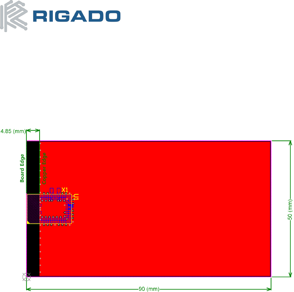
11.1 Recommended RF layout and Ground Plane
The integrated antenna on the R41Z module requires a suitable ground plane to radiate effectively. The
module antenna has been tuned for having a PCB directly below with no copper or any other metal
present. The module should be placed at the edge of the PCB with the antenna edge facing out. For best
performance, the ground plane should be on the same layer as the module or as close as possible. If this
is not possible in a design, ground planes on multiple layers generously connected with vias may also be
used. Reduced ground plane size will result in reduced radio performance.
Figure 13 - R41Z RF Example Based on EVAL Board
11.2 Mechanical Enclosure
Care should be taken when designing and placing the module into an enclosure. Metal should be kept
clear from the antenna area, both above and below. Any metal around the module can decrease RF
performance.
The module is designed and tuned to be in free air. Any potting, epoxy fill, plastic over-molding, or
conformal coating can negatively impact RF performance and must be evaluated by the customer. If
potting must be used, the compound should have a low dielectric constant and should be designed for
use with 2.4GHz RF electronics.

R41Z Module Data Sheet
Thread + Bluetooth 4.2 LE
November 17, 2016
R41Z-DS-1.0 Page 21 of 30
11.3 Antenna Patterns
11.3.1 X-Y Plane
TBD
11.3.2 Y-Z Plane
TBD
11.3.3 Z-X Plane
TBD
12. Evaluation Boards
Rigado has developed a full featured evaluation board that provides on-board programming and debug,
power and virtual COM port over USB, 32.768kHz crystal, Arduino style IO headers 2 mechanical user
buttons, 2 capacitive touch buttons, 3-axis accelerometer/magnetometer (I2C), and a 4Mbit flash chip
(SPI). The evaluation board also allows for easy use of all of the R41Z’s DCDC power modes and can be
powered from an adjustable LDO regulator, CR2032 coin cell battery, or through an external power
header. Power consumption can be measured through onboard current sensing resistors and headers.
Figure 14 - R41Z Evaluation Board
R41Z Module Data Sheet
Thread + Bluetooth 4.2 LE
November 17, 2016
R41Z-DS-1.0 Page 22 of 30
13. Custom Development
Rigado is a full-service design house offering end-to-end product development from concept to
manufacturing. We can provide custom modules, perform electrical and mechanical design, end product
manufacturing, firmware and mobile development, and DevOps management tools.
14. Bluetooth Qualification
The R41Z module is being qualified as a Bluetooth Component (tested) for RF-PHY. This allows for
customers to use qualified NXP Bluetooth stacks without the need to complete additional RF-PHY
testing.
R41Z: Declaration ID TBD / QDID TBD
15. Regulatory Statements
15.1 FCC Statement
This device has been tested and found to comply with part 15 of the FCC rules. These limits are designed
to provide reasonable protection against harmful interference in a residential installation. This
equipment generates, uses and can radiate radio frequency energy and, if not installed and used in
accordance with the instructions, may cause harmful interference to radio communications. However,
there is no guarantee that interference will not occur in a particular installation. If this equipment does
cause harmful interference to radio or television reception, which can be determined by turning the
equipment off and on, the user is encouraged to try to correct the interference by one or more of the
following measures:
Reorient or relocate the receiving antenna.
Increase the separation between the equipment and the receiver
Connect the equipment into an outlet on a circuit different from that to which the receiver is
connected.
Consult the dealer or an experienced radio/TV technician for help.

R41Z Module Data Sheet
Thread + Bluetooth 4.2 LE
November 17, 2016
R41Z-DS-1.0 Page 23 of 30
Operation is subjected to the following two conditions: (1) This device may no cause harmful
interference, and (2) this device must accept any interference received, including interference that may
cause undesired operation. Note: Modification to this product will void the user’s authority to operate
this equipment.
Note: Modification to this product will void the users’ authority to operate this equipment.
15.2 FCC Important Notes:
(1) FCC Radiation Exposure Statement
This equipment complies with FCC RF radiation exposure limits set forth for an uncontrolled
environment. This transmitter must not be co-located or operating in conjunction with any other
antenna or transmitter.
This equipment complies with Part 15 of the FCC Rules. Operation is subject the following two
conditions:
(1) This device may not cause harmful interference, and
(2) This device must accept any interference received, including interference that may cause undesired
operation.
The devices must be installed and used in strict accordance with the manufacturer’s instructions as
described in this document.
Caution!
The manufacturer is not responsible for any radio or TV interference caused by unauthorized
modifications to this equipment. Such modification could void the user authority to operate the
equipment.
(2) Co-location Warning:
This device and its antenna(s) must not be co-located or operating in conjunction with any other
transmitter antenna.
(3) OEM integration instructions:
This device is intended only for OEM integrators under the following conditions:
The antenna and transmitter must not be co-located with any other transmitter or antenna. The module
shall be only used with the integral antenna(s) that has been originally tested and certified with this
module.
As long as the two (2) conditions above are met, further transmitter testing will not be required.
However, the OEM integrator is still responsible for testing their end-product for any additional
compliance requirements with this module installed (for example, digital device emission, PC peripheral
requirements, etc.)
In the event that these conditions cannot be met (for example certain laptop configuration or co-
location with another transmitter), then the FCC authorization for this module in combination with the

R41Z Module Data Sheet
Thread + Bluetooth 4.2 LE
November 17, 2016
R41Z-DS-1.0 Page 24 of 30
host equipment is no longer considered valid and the FCC ID of the module cannot be used on the final
product. In these and circumstance, the OEM integrator will be responsible for re-evaluating. The end
product (including the transmitter) and obtaining a separate FCC authorization.
Caution!
The OEM is still responsible for verifying compliance with FCC Part 15, subpart B limits for
unintentional radiators through an accredited test facility.
(4) End product labeling:
The final end product must be labeled in a visible area with the following:
“Contains FCC ID: 2AA9B07”
Any similar wording that expresses the same meaning may be used.
The FCC Statement below should also be included on the label. When not possible, the FCC Statement
should be included in the User Manual of the host device.
“This device complies with part 15 of the FCC rules.
Operation is subject to the following two conditions. (1) This device may not cause harmful interference.
(2) This device must accept any interference received, including interference that may cause undesired
operation.”
(5) Information regarding the end user manual:
The OEM integrator has to be aware not to provide information to the end user regarding how to install
or remove this RF module in the user’s manual of the end product which integrates this module. The
end user manual shall include all required regulatory information/warning as show in this manual
(Section 15.2(4)).
15.3 IC Statement:
This device complies with Industry Canada license-exempt RSS standard(s). Operation is subject to the
following two conditions: (1) this device may not cause interference, and (2) this device must accept any
interference, including interference that may cause undesired operation of the device.
Le présent appareil est conforme aux CNR d'Industrie Canada applicables aux appareils radio exempts de
licence. L'exploitation est autorisée aux deux conditions suivantes : (1) l'appareil ne doit pas produire de
brouillage, et (2) l'utilisateur de l'appareil doit accepter tout brouillage radioélectrique subi, même si le
brouillage est susceptible d'en compromettre le fonctionnement.
RF exposure warning: The equipment complies with RF exposure limits set forth for an uncontrolled
environment. The antenna(s) used for this transmitter must not be co-located or operating in
conjunction with any other antenna or transmitter.

R41Z Module Data Sheet
Thread + Bluetooth 4.2 LE
November 17, 2016
R41Z-DS-1.0 Page 25 of 30
Avertissement d'exposition RF: L'équipement est conforme aux limites d'exposition aux RF établies pour
un incontrôlés environnement. L'antenne (s) utilisée pour ce transmetteur ne doit pas être co-localisés
ou onctionner en conjonction avec toute autre antenne ou transmetteur .
15.4 IC Important Notes:
1. The OEM integrator has to be aware not to provide information to the end user regarding how to
install or remove this RF module in the user manual of the end product.
The user manual which is provided by OEM integrators for end users must include the following
information in a prominent location.
2. To comply with IC RF exposure compliance requirements, the antenna used for this transmitter must
not be co‐located or operating in conjunction with any other antenna or transmitter, except in
accordance with IC multi‐transmitter product procedures.
3. The final system integrator must ensure there is no instruction provided in the user manual or
customer documentation indicating how to install or remove the transmitter module except such device
has implemented two‐ways authentication between module and the host system.
4. The host device shall be properly labelled to identify the module within the host device. The final end
product must be labeled in a visible area with the following:
“Contains IC: 12208A-07“
Any similar wording that expresses the same meaning may be used.
The IC Statement below should also be included on the label. When not possible, the IC Statement
should be included in the User Manual of the host device.
“This device complies with Industry Canada license-exempt RSS standard(s). Operation is subject to the
following two conditions: (1) this device may not cause interference, and (2) this device must accept any
interference, including interference that may cause undesired operation of the device.
Le présent appareil est conforme aux CNR d'Industrie Canada applicables aux appareils radio exempts de
licence. L'exploitation est autorisée aux deux conditions suivantes : (1) l'appareil ne doit pas produire de
brouillage, et (2) l'utilisateur de l'appareil doit accepter tout brouillage radioélectrique subi, même si le
brouillage est susceptible d'en compromettre le onctionnement.”
15.5 CE Regulatory:
The R41Z modules are being tested and expected to be compliant against the following standards. OEM
integrators should consult with qualified test house to verify all regulatory requirements have been met
for their complete device.
From Directive 2006/95/EC:
EN 60950-1: 2006 + A11: 2009 + A1: 2010 + A12: 2011
From R&TTE Directive 1999/5/EC:
ETSI EN 300 328 V 1.9.1

R41Z Module Data Sheet
Thread + Bluetooth 4.2 LE
November 17, 2016
R41Z-DS-1.0 Page 26 of 30
From Directive 2004/108/EC:
ETSI EN 301 489-1 V1.9.2
ETSI EN 301 489-17 V2.2.1
Declarations of Conformity and supporting test reports are available at www.rigado.com.
15.6 Japan (MIC)
The R41Z Series modules are pending type certification and are to be labeled with its own technical
conformity mark and certification number as required to conform to the technical standards regulated
by the Ministry of Internal Affairs and Communications (MIC) of Japan pursuant to the Radio Act of
Japan. Integration of this module into a final end product does not require additional radio certification
provided installation instructions are followed and no modifications of the module are allowed.
Additional testing may be required:
• If the host product is subject to electrical appliance safety (for example, powered from an AC
mains), the host product may require Product Safety Electrical Appliance and Material (PSE)
testing. The integrator should contact their conformance laboratory to determine if this testing
is required.
• There is a voluntary Electromagnetic Compatibility (EMC) test for the host product administered
by VCCI: http://www.vcci.jp/vcci_e/index.html
The label on the final end product which contains a R41Z Series module must follow the MIC marking
requirements. Labeling requirements for Japan available at the Ministry of Internal Affairs and
Communications (MIC) website: http://www.tele.soumu.go.jp/e/index.htm.
The R41Z module is to be labeled with its assigned technical conformity mark and certification number.
The final end product in which this module is being used must have an external label referring to the
type certified module inside:
Contains transmitter module with certificate number:
15.7 Australia / New Zealand
The R41Z module have been tested to comply with the AS/NZS 4268 :2012+AMDT 1:2013, Radio
equipment and systems – Short range devices – Limits and methods of measurement. The report
(Pending) may be downloaded from www.rigado.com, and may be used as evidence in obtaining
permission to use the RCM.
Information on registration as a Responsible Party, license and labeling requirements may be found at
the following websites:
TBD
R41Z Module Data Sheet
Thread + Bluetooth 4.2 LE
November 17, 2016
R41Z-DS-1.0 Page 27 of 30
Australia: http://www.acma.gov.au/theACMA/radiocommunications-short-range-devices-standard-
2004
New Zealand: http://www.rsm.govt.nz/compliance
The A-Tick and C-Tick marks are being migrated to the Regulatory Compliance Mark (RCM). Only
Australian-based and New Zealand-based companies who are registered may be granted permission to
use the RCM. An Australian-based or New Zealand-based agent or importer may also register as a
Responsible Party to use the RCM on behalf of a company not in Australia or New Zealand.
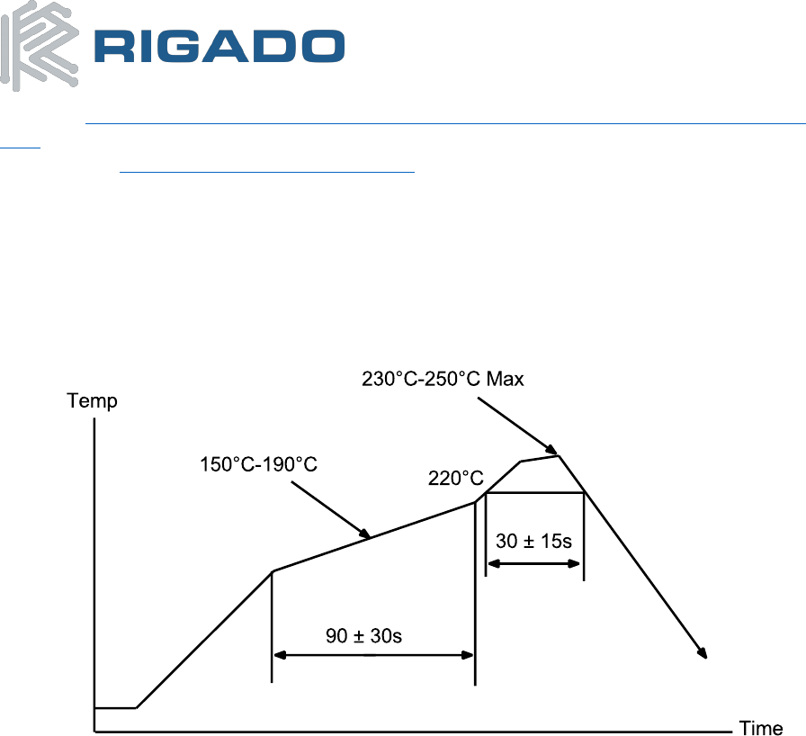
16. Solder Reflow Temperature-Time Profile
Figure 15 - Reflow Profile for Lead Free Solder
16.1 Moisture Sensitivity Level
The R41Z module is rated for MSL 3, 168-hour floor life after opening.
R41Z Module Data Sheet
Thread + Bluetooth 4.2 LE
November 17, 2016
R41Z-DS-1.0 Page 28 of 30
17. Packaging and Labeling
17.1 Carrier Tape Dimension
TBD
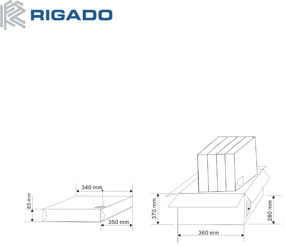
17.2 Reel Packaging
Modules come on 330mm reels loaded with 1000 modules. Each reel is placed in an antistatic bag
with a desiccant pack and humidity card and placed in a 340x350x65mm box. On the outside of the
bag an antistatic warning and reel label are adhered.
Figure 16 - Reel Cartons

R41Z Module Data Sheet
Thread + Bluetooth 4.2 LE
November 17, 2016
R41Z-DS-1.0 Page 29 of 30
17.3 Packaging Label
Figure 17 - Packaging Label
18. Cautions
1) The guidelines of this document should be followed in order to assure proper performance of
the module.
2) This product is for use in office, business, and residential applications, but not medical devices.
3) This module may short-circuit. If a short circuit can result in serious damage or injury then
failsafe precautions should be used. This could be accomplished by redundant systems and
protection circuits.
4) Supply voltage to the module should not be higher than the specified inputs or reversed.
Additionally, it should not contain noise, spikes, or AC ripple voltage.
5) Avoid use with other high frequency circuits.
6) Use methods to eliminate static electricity when working with the module as it can damage the
components.
7) Contact with wires, the enclosure, or any other objects should be avoided.
8) Refer to the recommended pattern when designing for this module.
9) If hand soldering is used, be sure to use the precautions outlined in this document.
10) This module should be kept away from heat, both during storage and after installation.
11) Do not drop or physically shock the module.
12) Do not damage the interface surfaces of the module.
13) The module should not be mechanically stressed at any time (storage, handling, installation).
14) Do not store or expose this module to:
Humid or salty air conditions
High concentrations of corrosive gasses.
Long durations of direct sunlight.
Temperatures lower than -40°C or higher than 125°C.
R41Z Module Data Sheet
Thread + Bluetooth 4.2 LE
November 17, 2016
R41Z-DS-1.0 Page 30 of 30
19. Life Support Policy
This product is not designed to be used in a life support device or system, or in applications where there
is potential for a failure or malfunction to, directly or indirectly, cause significant injury. By using this
product in an application that poses these risks, such as described above, the customer is agreeing to
indemnify Rigado for any damages that result.
20. Document History
Revision
Date
Changes / Notes
0.9
10/20/2016
Release draft. Images and specifications updated.
1.0
11/17/2016
Certifications added
21. Related Documents
Rigado Documents:
R41Z Module Product Brief
NXP Documents:
KW41Z Fact Sheet
NXP BLE Mobile Toolbox
KW41Z Data Sheet
KW41Z Reference Manual