u blox LUCYH200 Quadband GSM/GPRS and Triband UMTS/HSDPA wireless module User Manual LUCY H200
u-blox AG Quadband GSM/GPRS and Triband UMTS/HSDPA wireless module LUCY H200
u blox >
Contents
- 1. Users manual
- 2. Users Manual
Users manual
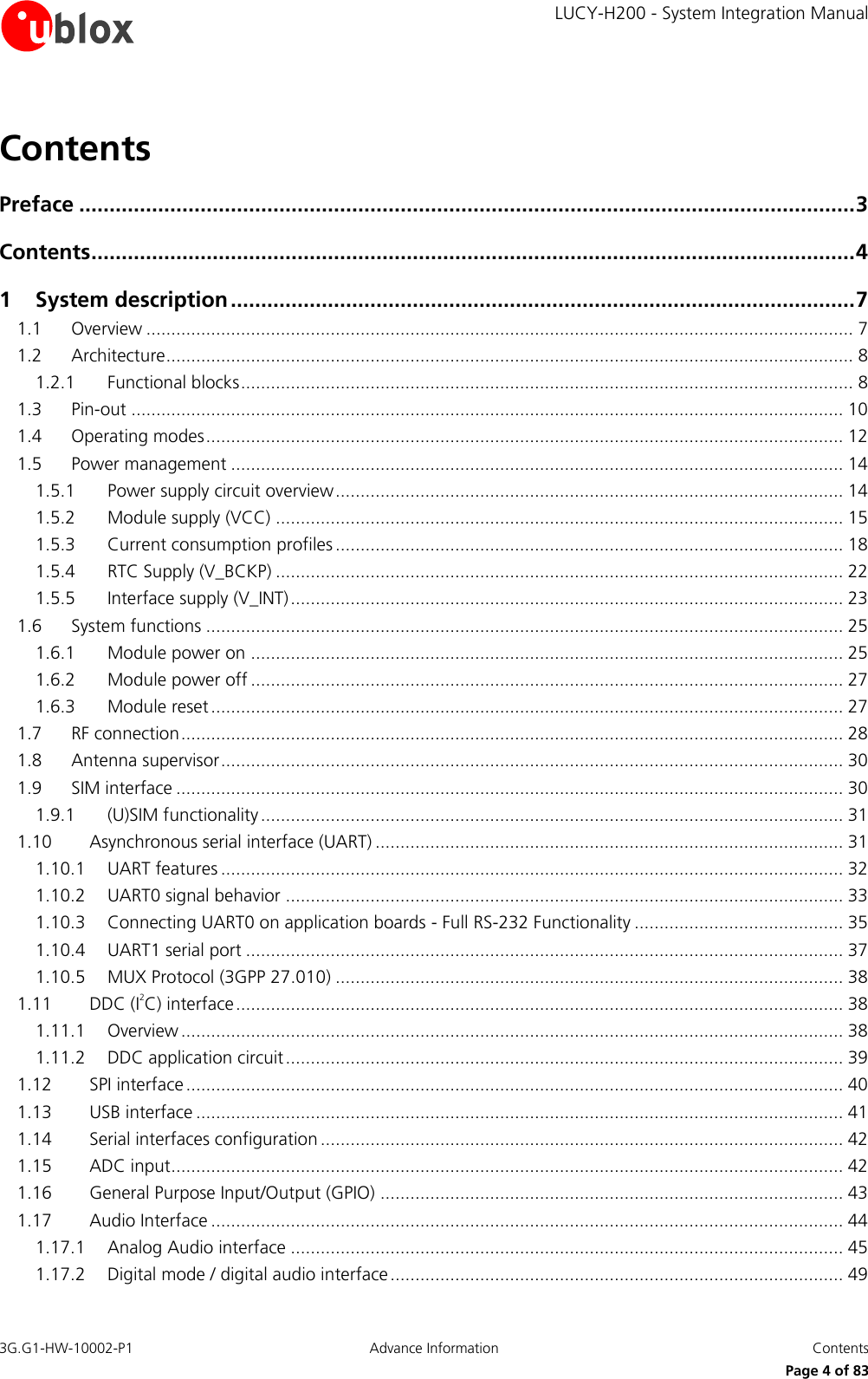
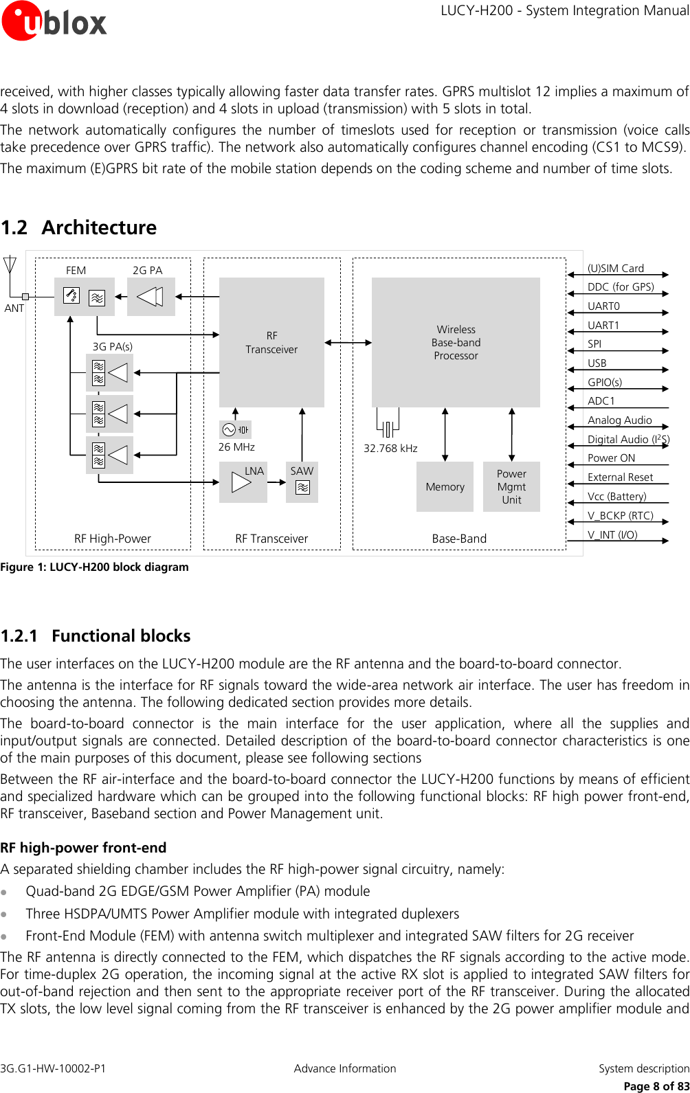
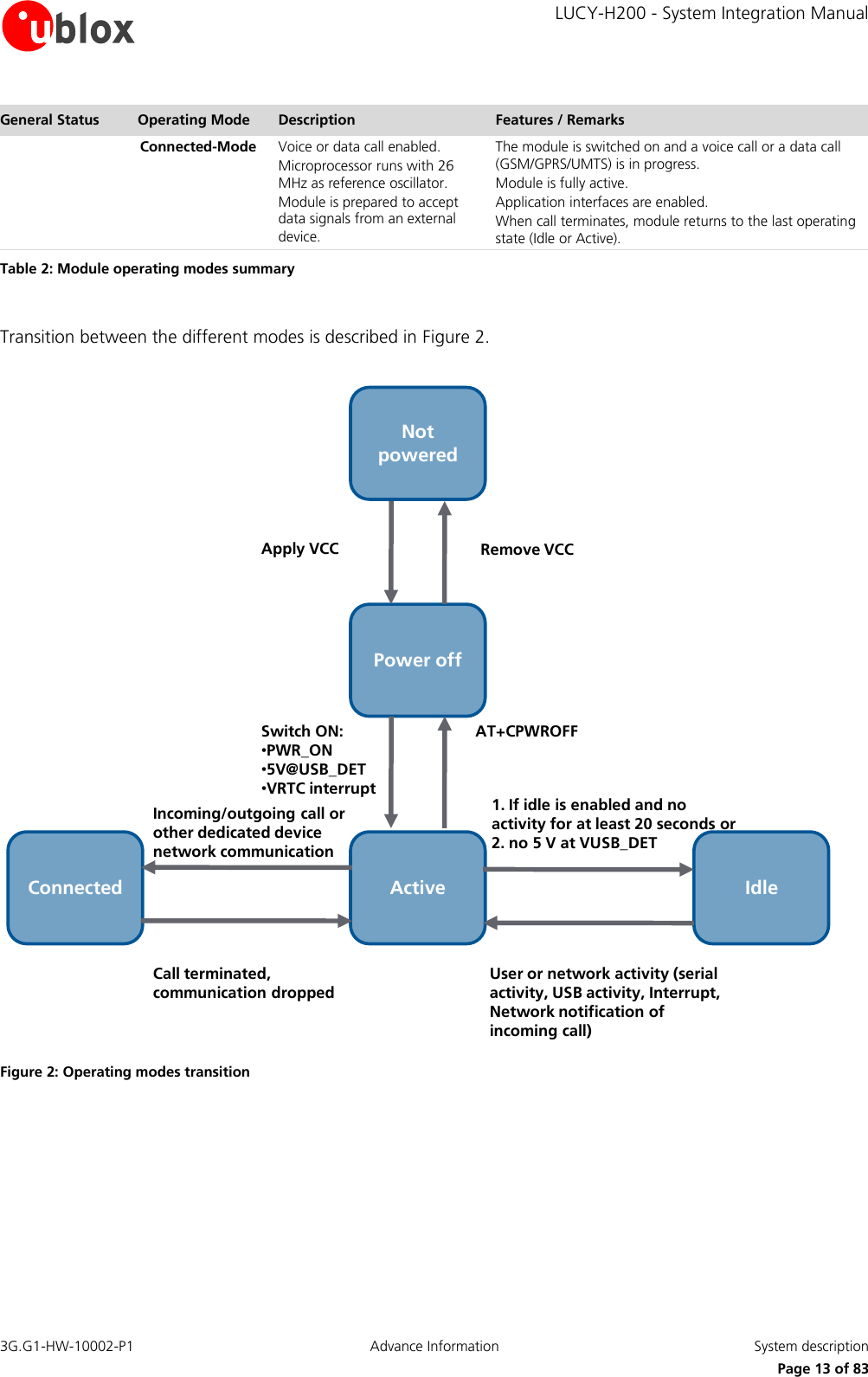
![LUCY-H200 - System Integration Manual 3G.G1-HW-10002-P1 Advance Information System description Page 12 of 83 1.4 Operating modes The LUCY-H200 module includes several operating modes, each have different active features and interfaces. Table 2 summarizes the various operating modes and provides general guidelines for operation. General Status Operating Mode Description Features / Remarks Power-down Not-Powered Mode VCC supply not present or below normal operating range. Microprocessor not operating. RTC only operates if supplied through V_BCKP pin. Module is switched off. Module cannot be switched on by a falling edge provided on the PWR_ON input, neither by a preset RTC alarm, or a rising edge to a valid range of USB voltage provided on the VUSB_DET input. Application interfaces not accessible. Internal RTC timer operates only if a valid voltage is applied to V_BCKP pin. Power-Off Mode VCC supply within normal operating range. Microprocessor not operating. Only RTC runs. Module is switched off: normal shutdown after sending the AT+CPWROFF command (refer to u-blox 3.5G HSDPA AT Commands Manual [2]). Module can be switched on by a falling edge provided on the PWR_ON input, by a preset RTC alarm, or a rising edge to a valid voltage for USB VBUS detection provided on the VUSB_DET inputs. Application interfaces are not accessible. Only the internal RTC timer in operation. Normal operation Idle-Mode Microprocessor runs with 32 kHz as reference oscillator. Module does not accept data signals from an external device. Module is switched on and is in idle mode (i.e. power saving / sleep mode). Application interfaces disabled. Module by default does not enter automatically in idle mode; this happens only if this mode is enabled by appropriate AT command (refer to u-blox 3.5G HSDPA AT Commands Manual [2]). If module is registered with the network, and idle mode is enabled, it automatically enters idle mode and periodically wakes up to active mode to monitor the paging channel for the paging block reception according to network indication. If module is not registered with the network, and idle mode is enabled, it automatically goes in idle mode and periodically wakes up to monitor external activity. Module wakes up from idle mode to active mode if an RTC alarm occurs. Module wakes up from idle mode to active mode when data received on UART interface with HW flow control enabled. Module wakes up from idle mode to active mode if a voice or data call incoming. Module wakes up from idle mode to active mode when the RTS input line is set to the ON state by the DTE if the AT+UPSV=2 command is sent to the module (feature not enabled by default). The hardware flow control output (CTS line) indicates when the module is in idle (power saving mode): the line is driven in the OFF state when the module is not prepared to accept data signals. Module wakes up from idle mode to active mode if a valid VBUS voltage is detected on VUSB_DET pin: the UART0 interface is then disabled and USB becomes active. When USB is active, the external interface connected to UART0 RTS_0 and CTS_0 should be tri-stated , see section 1.13 Active-Mode Microprocessor runs with 26 MHz as reference oscillator. The module is prepared to accept data signals from an external device. Module is switched on and is fully active: power saving is not enabled. The application interfaces are enabled.](https://usermanual.wiki/u-blox/LUCYH200.Users-manual/User-Guide-1320517-Page-12.png)
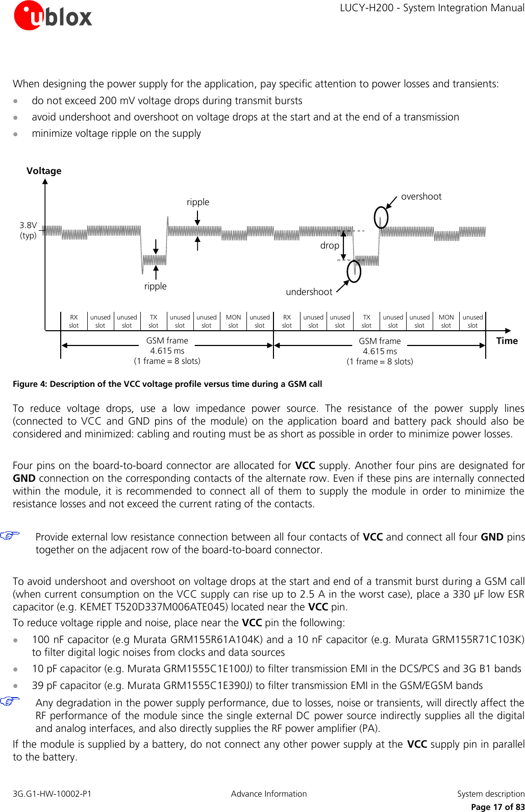
![LUCY-H200 - System Integration Manual 3G.G1-HW-10002-P1 Advance Information System description Page 16 of 83 power capabilities: the switching regulator with its output circuit must be capable of providing a valid voltage value to the VCC pin and must be capable of delivering 2.5 A current pulses with 1/8 duty cycle to the VCC pin low output ripple: the switching regulator with its output circuit must be capable of providing a clean (low noise) VCC voltage profile fixed switching frequency greater or equal to 1 MHz: variable or lower switching frequency will produce noise in the VCC voltage profile so that the module will not reach the GSM modulation spectrum requirements fixed PWM mode operation: PFM mode and PFM/PWM modes transitions must be avoided to reduce the noise on the VCC voltage profile The characteristics of the rechargeable Li-Ion battery connected to the VCC pin should meet the following requirements: maximum DC/pulse discharge current: the rechargeable Li-Ion battery with its output circuit must be capable of delivering 2.5 A current pulses with 1/8 duty cycle to the VCC pin DC series resistance: the rechargeable Li-Ion battery with its output circuit must be capable of avoiding a VCC voltage drop greater than 400 mV The characteristics of the primary (not rechargeable) battery connected to the VCC pin are compliant with the following requirements: maximum DC/pulse discharge current: the not-rechargeable battery with its output circuit must be capable of delivering 2.5 A current pulses with 1/8 duty cycle to the VCC pin DC series resistance: the rechargeable Li-Ion battery with its output circuit must be capable of avoiding a VCC voltage drop greater than 400 mV The voltage provided to the VCC pin must be within the normal operating range limits specified in the LUCY-H200 Data Sheet [1]. Complete functionality of the module is only guaranteed within the specified minimum and maximum VCC voltage range. Ensure that the input voltage at VCC is above the normal operating range minimum limit to enable the switch-on of the module. Note that the module cannot be switched on if the VCC voltage value is below the minimum specified limit. See the LUCY-H200 Data Sheet [1]. When the LUCY-H200 module is in operation, the voltage provided to the VCC pin can exceed the normal operating range limits but must be within the extended operating range limits specified in the LUCY-H200 Data Sheet [1]. Module reliability is only guaranteed within this specified operational extended voltage range. Ensure that the input voltage at the VCC pin never drops below the extended operating range minimum limit when the module is switched on, not even during a GSM transmit burst, where the current consumption can rise up to peaks of 2.5 A in case of a mismatched antenna load. The module switches off when the VCC voltage value drops below the minimum limit. Operation above the extended operating range maximum limit is not recommended and extended exposure beyond it may affect device reliability. Stress beyond the VCC absolute maximum ratings may cause permanent damage to the module: if necessary, voltage spikes beyond VCC absolute maximum ratings must be limited to values within the specified boundaries by using appropriate protection.](https://usermanual.wiki/u-blox/LUCYH200.Users-manual/User-Guide-1320517-Page-16.png)
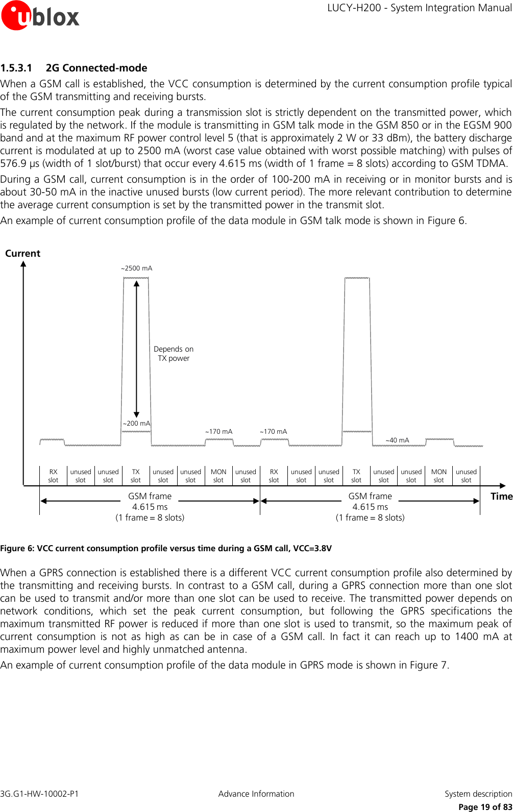
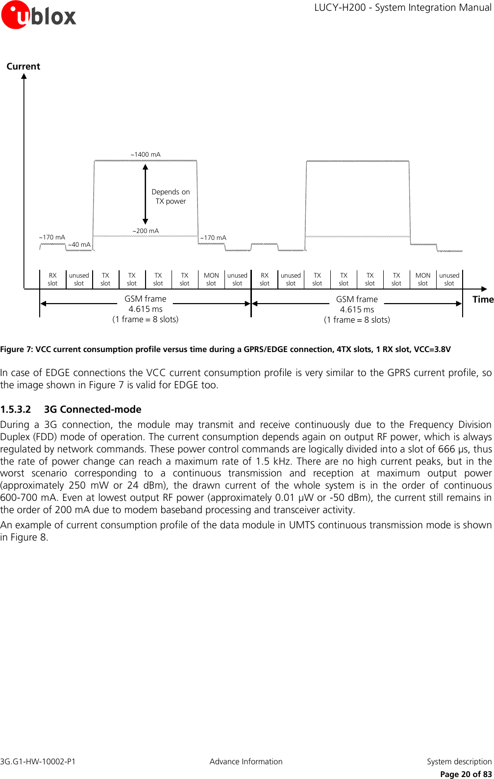
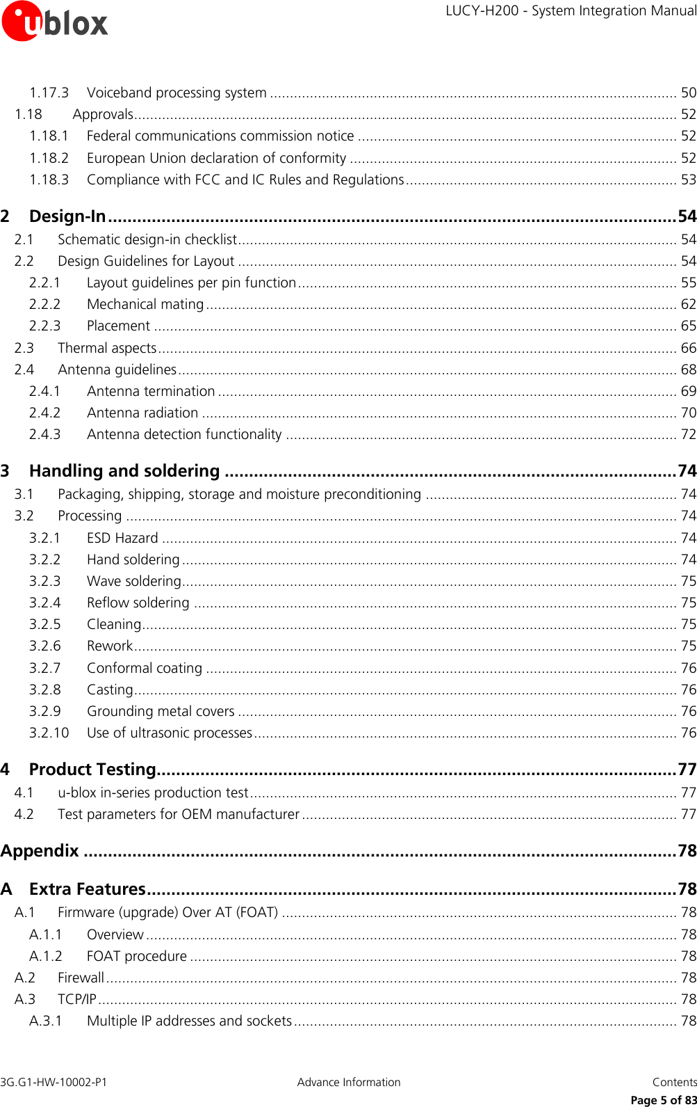
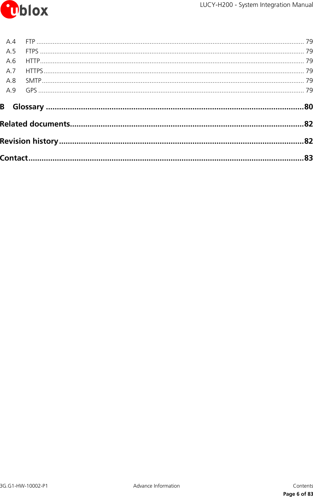
![LUCY-H200 - System Integration Manual 3G.G1-HW-10002-P1 Advance Information System description Page 21 of 83 Time3G frame 10 ms (1 frame = 15 slots)Current170 mA650 mADepends on TX power1 slot 666 µs Figure 8: VCC current consumption profile versus time during a UMTS connection, VCC=3.8V When a packet data connection is established, the actual current profile depends on the amount of transmitted packets; there might be some periods of inactivity between allocated slots where current consumption drops about 100 mA. Alternatively, at higher data rates the transmitted power is likely to increase due to the higher quality signal required by the network to cope with enhanced data speed. 1.5.3.3 Idle-mode By default the module does not automatically enter idle-mode (power-saving mode) whenever possible; idle mode must be enabled using the appropriate AT command (refer to u-blox 3.5G HSDPA AT Commands Manual [2]). When the data module is registered or attached to a network and a voice or data call is not enabled, the module must periodically monitor the paging channel of the current base station (paging block reception), in accordance to GSM and UMTS system requirements. When the module monitors the paging channel, it wakes up to active mode, to enable the paging block reception. In between, the module switches to idle-mode (power-saving mode). This is known as discontinuous reception (DRX). The module processor core is activated during the paging block reception, and automatically switches its reference clock frequency from the 32 kHz to the 26 MHz used in active-mode. The time period between two paging block receptions is defined by the network. For example, the time interval between two paging block receptions for 2G operation can be from 470.76 ms (width of 2 GSM multiframes = 2 x 51 GSM frames = 2 x 51 x 4.615 ms) up to 2118.42 ms (width of 9 GSM multiframes = 9 x 51 frames = 9 x 51 x 4.615 ms): this is the paging period parameter, fixed by the base station through broadcast channel sent to all users on the same serving cell. An example of a data module current consumption profile is shown in Figure 9: the module is registered with a 2G network, automatically goes into idle mode and periodically wakes up to active mode to monitor the paging channel for paging block reception](https://usermanual.wiki/u-blox/LUCYH200.Users-manual/User-Guide-1320517-Page-21.png)
![LUCY-H200 - System Integration Manual 3G.G1-HW-10002-P1 Advance Information System description Page 22 of 83 ~150 mA500-700 µA500-700 uA8-10 mA20-22 mA~150 mA0.44-2.09 s~30 msActive Mode EnabledIdle Mode EnabledPLL EnabledRX+DSP EnabledIDLE MODE ACTIVE MODE IDLE MODEIDLE MODE~30 msACTIVE MODECurrentTime Figure 9: Description of the VCC current consumption profile versus time when the module is registered on the GSM network: the module is in idle mode and periodically wakes up to active mode to monitor the paging channel for paging block reception 1.5.4 RTC Supply (V_BCKP) The V_BCKP pin connects the supply for Real Time Clock (RTC) and Power On / Reset internal logic. This supply domain is internally generated by a linear regulator integrated in the power management unit. The output of this linear regulator is always enabled when the main voltage supply provided to the module through VCC is within the valid operating range, being the module switched-off or powered-on. The RTC provides the time reference (date and time) of the module, also in power-off mode, when the V_BCKP voltage is within its valid range (specified in u-blox LUCY-H200 Data Sheet [1]). The RTC timing is normally used to set the wake-up interval during idle-mode periods between network paging, but is able to provide programmable alarm functions by means of the internal 32.768 kHz clock. The RTC can be supplied from an external back-up battery through the V_BCKP, when the main voltage supply is not provided to the module through VCC. This lets the time reference (date and time) run even when the main supply is not provided to the module. Please consider that the module cannot switch on if a valid voltage is not present on VCC even when RTC is supplied through V_BCKP (meaning that VCC is mandatory to switch-on the module). The RTC has very low power consumption, but is highly temperature dependent. For example at 25°C and a V_BCKP voltage of 2.0 V the power consumption is approximately 2 µA, whereas at 70°C and an equal voltage the power consumption increases to 5-10 µA. The internal regulator for V_BCKP is optimized for low leakage current and very light loads. It is recommended to not use V_BCKP to supply external loads.](https://usermanual.wiki/u-blox/LUCYH200.Users-manual/User-Guide-1320517-Page-22.png)
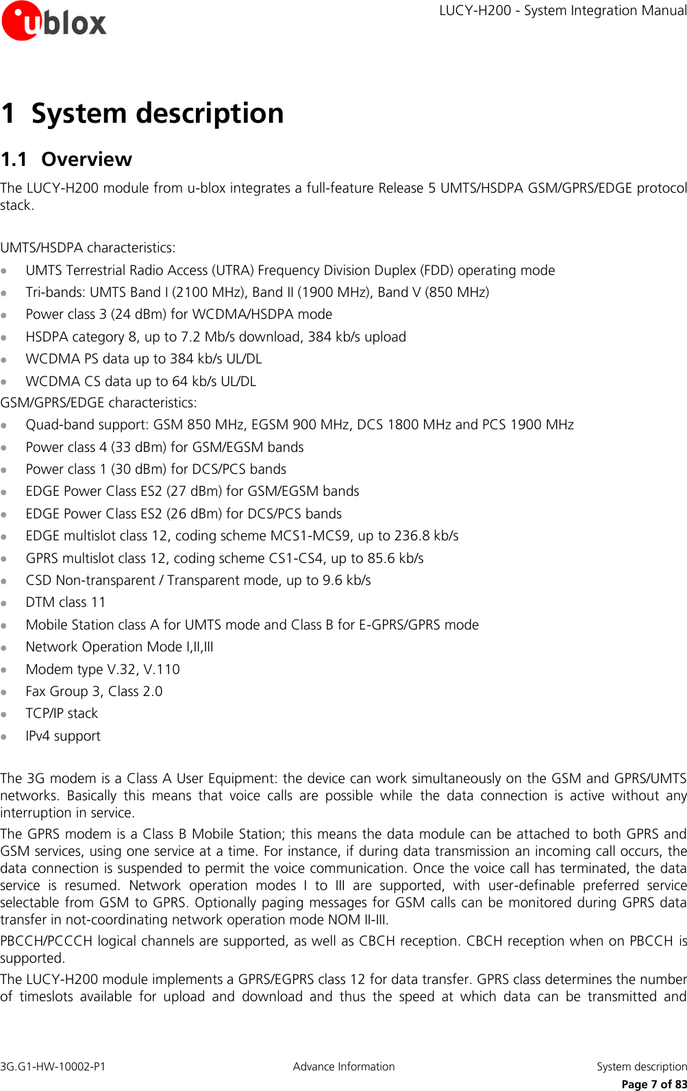
![LUCY-H200 - System Integration Manual 3G.G1-HW-10002-P1 Advance Information System description Page 23 of 83 If V_BCKP is left unconnected and the module main voltage supply is removed from VCC, the RTC is supplied from the 1 µF buffer capacitor mounted inside the module. However, this capacitor is not able to provide a long buffering time: within 0.5 seconds the voltage on V_BCKP will go below the valid range (1 V min). At this time the internal RTC will stop counting and the date and time setting will be lost. This has no impact on wireless connectivity, as all the functionalities of the module do not rely on the date and time setting. V_BCKP shall be left unconnected if the RTC is not required when the VCC supply is removed. The date and time will not be updated when VCC is disconnected. If VCC is always supplied, then the internal regulator will take input from the main supply and there is no need for an external component on V_BCKP. If RTC is required to run for a time interval of T [seconds] at 25°C when VCC supply is removed, place a capacitor with a nominal capacitance of C [µF] at the V_BCKP pin. Choose the capacitor using the following formula: C [µF] = (Current_Consumption [µA] x T [seconds]) / Voltage_Drop [V] = 2 x T [seconds] The current consumption of the RTC is approximately 2 µA at 25°C, and the voltage drop is equal to 1 V (from the V_BCKP typical value of 2.0 V to the valid range minimum limit of 1.0 V). For example, a 100 µF capacitor (such as the Murata GRM43SR60J107M) can be placed at V_BCKP to provide a long buffering time. This capacitor will hold V_BCKP voltage within its valid range for around 50 seconds at 25°C, after the VCC supply is removed. If a very long buffering time is required, a 70 mF super-capacitor (e.g. Seiko Instruments XH414H-IV01E) can be placed at V_BCKP, with a 4.7 kΩ series resistor to hold the V_BCKP voltage within its valid range for around 10 hours at 25°C, after the VCC supply is removed. These capacitors will allow the time reference to run during battery disconnection. 2100 µF GRM43SR60J107M70 mFXH414H-IV01E 4.7 kLUCY-H20055 V_BCKP2LUCY-H20055 V_BCKP Figure 10: Real time clock supply (V_BCKP) application circuits using a 100 µF capacitor to let the RTC run for ~50 seconds at 25°C or using a 70 mF capacitor to let the RTC run for ~10 hours at 25°C when the VCC supply is removed 1.5.5 Interface supply (V_INT) The same voltage domain used internally to supply the digital interfaces is also available at the board-to-board connector on pin V_INT. The internal regulator is a switching step down converter: it is directly supplied from VCC and output voltage is set to 1.8 V (typical). It operates in Pulse Width Modulation (PWM) for high output current mode but automatically switches to Pulse Frequency Modulation (PFM) at low output loads for greater efficiency, e.g. when the module is in idle mode between paging periods.](https://usermanual.wiki/u-blox/LUCYH200.Users-manual/User-Guide-1320517-Page-23.png)
![LUCY-H200 - System Integration Manual 3G.G1-HW-10002-P1 Advance Information System description Page 25 of 83 1.6 System functions 1.6.1 Module power on When supply is connected to the VCC pin, the voltage supervision circuit controls the subsequent activation of the power up state machines. The module power-on sequence is initiated in one of 3 ways: Falling edge on the PWR_ON signal RTC alarm Detection on pin VUSB_DET of a valid VUSB voltage (typical 5V) for USB detection Name Description Remarks PWR_ON Power-on input PWR_ON pin has an internal pull-up resistor to V_BCKP. Nevertheless provide space for mounting an external pull up resistor on the application board in case of noisy environment, where an external pull-up is required Table 5: Power-on pin 1.6.1.1 Falling edge on the PWR_ON The module power-on sequence starts when a low level is forced on the PWR_ON signal. The electrical characteristics of the PWR_ON input pin are different from the other digital I/O interfaces: the high and the low logic levels have different operating ranges and the pin is tolerant of voltages only up to the V_BCKP voltage. The nominal V_BCKP pin voltage is 2 V; the detailed electrical characteristics are described in the LUCY-H200 Data Sheet [1]. The PWR_ON pin is pulled up to V_BCKP through an internal 470 kΩ resistor. To avoid floating in a noisy environment: a pull up resistor to V_BCKP supply can be added on the application board at least as a not mounting option. The boot time is around 1 second when the falling edge on the PWR_ON pin is used to power on the module. Note that the module can be switched-on by a falling edge on the PWR_ON pin. Once the module has turned on moving the PWR_ON pin has no effect. On the other hand it makes no sense to keep this pin low when the module is turned on as it would source some unnecessary µA. Following are some typical examples of turning the module on. The simplest way to turn on the module is to use a push button connected to ground.](https://usermanual.wiki/u-blox/LUCYH200.Users-manual/User-Guide-1320517-Page-25.png)
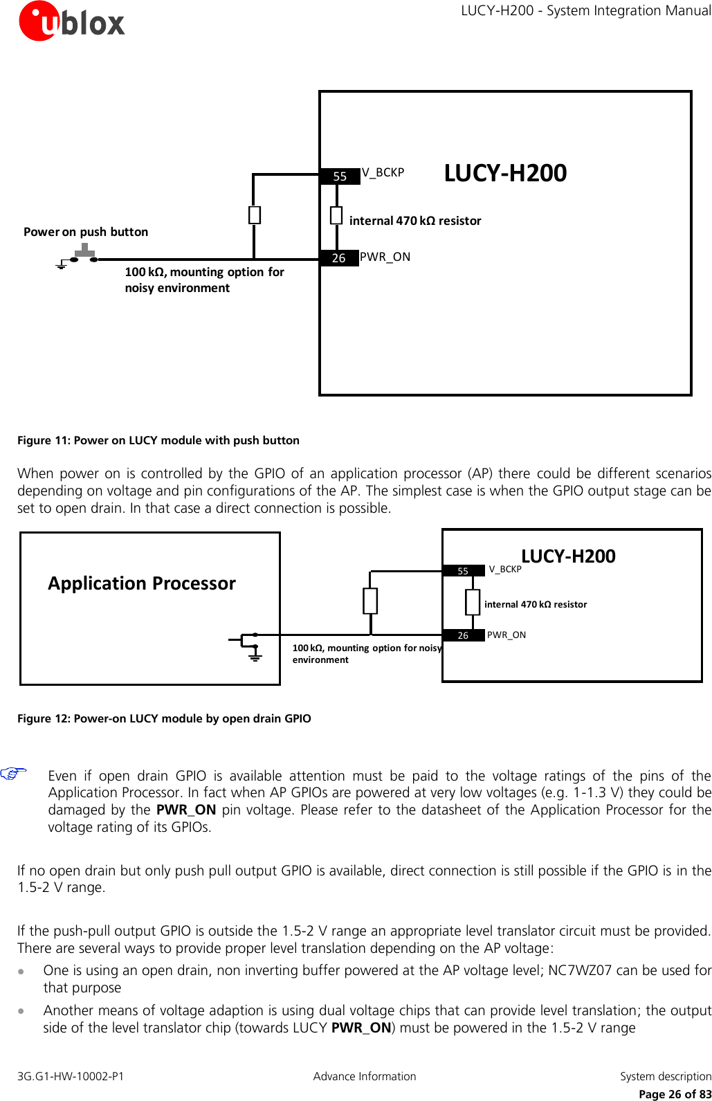
![LUCY-H200 - System Integration Manual 3G.G1-HW-10002-P1 Advance Information System description Page 27 of 83 Remember to fix the unused inputs of buffers or voltage translator chips with more ports than required to GND or to power in order to prevent increase in power consumption due to high impedance floating inputs. 1.6.1.2 Real Time Clock (RTC) alarm Power on If a valid voltage is maintained at the VCC pin, the module can be switched-on by the RTC alarm when the RTC system reaches a pre-programmed scheduled time. The RTC system will then initiate the boot sequence by indicating to the power management unit to turn on power. Also included in this setup is an interrupt signal from the RTC block to indicate to the baseband processor, that an RTC event has occurred. The boot time is around 1 second when the power on of the module is caused by RTC alarm. 1.6.1.3 Detection on pin VUSB_DET of a valid VUSB voltage If a valid VUSB voltage is detected on the VUSB_DET pin, the module turns on. Please refer to the LUCY-H200 Data Sheet [1] for the VUSB range that must be applied to VUSB_DET pin. When the power on cause is a valid VUSB voltage, USB block is turned on and UART0 is disabled. Once the module is powered, if voltage at VUSB_DET goes outside of the VUSB range, UART0 is re-enabled. The line that triggers power on at VUSB_DET pin must have less than 100 Ω impedance. When voltage at VUSB_DET pin is in the VUSB range the module does not enter idle state even if has been enabled by the appropriate AT command (for more details please refer to u-blox 3.5G HSDPA AT commands manual [2]). The boot time is around 3 seconds when the power on is caused by a USB range voltage (4.3 V-5.3 V, typically 5 V) at VUSB_DET pin. 1.6.2 Module power off The LUCY-H200 module can be switched off by one of the following switch-off events: Via AT command AT+CPWROFF (more details in u-blox 3.5G HSDPA AT Commands Manual [2]) An under-voltage shutdown will be done if VCC falls below the valid operating limit After a switch-off event has been triggered, the digital pins are locked in tri-state by the module. All internal voltage regulators, except the RTC supply, are turned off in a defined power-off sequence. 1.6.3 Module reset Reset the module using RESET_N: this performs an external or hardware reset. When the RESET_N pin is driven low, an asynchronous reset of the entire module - except for the RTC - is triggered, and the device is initialized into a defined reset state. Name Description Remarks RESET_N External reset input Internal pull-up Table 6: Reset pin The electrical characteristics of RESET_N are different from the other digital I/O interfaces. The detailed electrical characteristics are described in the LUCY-H200 Data Sheet [1]. RESET_N is pulled high by an integrated pull-up resistor. Therefore an external pull-up should be not required on the application board. An internal circuit pulls the level to 2.0 V. Forcing RESET_N low for at least 50 ms will cause an external reset of the module. When RESET_N is released from the low level, the module automatically starts its power-on reset sequence.](https://usermanual.wiki/u-blox/LUCYH200.Users-manual/User-Guide-1320517-Page-27.png)
![LUCY-H200 - System Integration Manual 3G.G1-HW-10002-P1 Advance Information System description Page 28 of 83 If RESET_N is connected to an external device (e.g. an application processor on an application board) an open drain output can be directly connected without any external pull-up. Otherwise, use a push-pull output. Make sure to fix the proper level on RESET_N in all possible scenarios, to avoid unwanted reset of the module. The reset state of all input-output pins is reported in the pin description table in the LUCY-H200 Data Sheet [1]. 1.7 RF connection The interface for RF signal (ANT) is available via the Hirose U.FL-SMT-R or equivalent sub-miniature coaxial connector. The ANT interface has a nominal impedance of 50 Ω, and must be connected to the antenna through a 50 Ω transmission line to allow transmission and reception of radio frequency (RF) signals in the GSM and UMTS operating bands. Name Description Remarks ANT RF antenna Zo = 50 nominal characteristic impedance. Hirose U.FL-SMT-R receptacle connector. Table 7: Antenna pin The RF receptacle implemented on the LUCY-H200 for ANT requires a suitable mated RF plug from the same connector series. Due to its wide usage in the industry, several manufacturers offer compatible equivalents. The board-to-board connector stacked mated height also limits the selection of the RF plug. Nevertheless the nominal 3 mm height of the board-to-board connector effectively allows the usage of all U.FL compatible plugs available on the market. Table 8 lists some RF connector plugs that fit LUCY-H200, based on the declaration of the respective manufacturers. Only the Hirose has been qualified for the LUCY-H200 module, contact other producers to verify compatibility. Manufacturer Series Remarks Hirose U.FL® Ultra Small Surface Mount Coaxial Connector Recommended I-PEX MHF® Micro Coaxial Connector Tyco UMCC® Ultra-Miniature Coax Connector Amphenol RF AMC® Amphenol Micro Coaxial LTI (Lighthorse Technologies, Inc) IPX ultra micro-miniature RF connector Table 8: U.FL compatible plug connector Typically the RF plug is available as a cable assembly: several kinds are available and the user should select the cable assembly best suited to the application. The key characteristics are: RF plug type: select U.FL or equivalent Cable thickness: typically from 0.8 mm to 1.37 mm Cable length: standard length is typically 100 mm or 200 mm, custom lengths may be available on request RF connector on other cable side: for example another U.FL (for board-to-board connection) or SMA (for panel mounting) The LUCY-H200 module is calibrated at the on-board U.FL receptacle: select thicker and shorter cables to minimize insertion loss. For applications requiring an internal integrated SMT antenna, it is suggested to use a U-FL-to-U.FL cable to provide RF path from the LUCY-H200 to PCB stripline or microstrip connected to antenna pads (see Figure 13). Take care that the PCB-to-RF-cable transition, stripline and antenna pads must be optimized for 50 Ω characteristic impedance.](https://usermanual.wiki/u-blox/LUCYH200.Users-manual/User-Guide-1320517-Page-28.png)
![LUCY-H200 - System Integration Manual 3G.G1-HW-10002-P1 Advance Information System description Page 30 of 83 1.8 Antenna supervisor Antenna detection is internally performed by the module via ANT. The RF port is DC coupled to the ADC unit in the baseband chip. The module measures the DC voltage at ANT, in the range of 0 to 2 V. Additionally, the module can inject a known DC current (~ 100 µA) on ANT and measures the resulting DC voltage. LUCY-H200ANTADCCurrent SourceRF ChokeDC BlockingFront-End RF Module Figure 14: Antenna Supervisor internal circuit If the DC voltage is present on ANT, or a DC connection to a known resistor at the radiating element is implemented, the module will be able to check the connection to the Antenna element. Refer to the u-blox 3.5G HSDPA AT Commands Manual [2] for more details on how to access this feature. 1.9 SIM interface An SIM card interface is provided on the board-to-board pins of the module: the high-speed SIM/ME interface is implemented as well as automatic detection of the required SIM supporting voltage. Both 1.8 V and 3 V SIM types are supported: activation and deactivation with automatic voltage switch from 1.8V to 3 V is implemented, according to ISO-IEC 7816-3 specifications. The SIM driver supports the PPS (Protocol and Parameter Selection) procedure for baud-rate selection, according to the values determined by the SIM Card. Table 9 describes the board to board pins related to the SIM interface: Name Description Remarks VSIM SIM supply 1.80 V typical or 2.90 V typical automatically generated by the module SIM_CLK SIM clock 3.25 MHz clock frequency SIM_IO SIM data Open drain, internal 4.7 kΩ pull-up resistor to VSIM SIM_RST SIM reset Table 9: SIM Interface pins Figure 15 shows the minimal circuit connecting the LUCY module and the SIM card.](https://usermanual.wiki/u-blox/LUCYH200.Users-manual/User-Guide-1320517-Page-30.png)
![LUCY-H200 - System Integration Manual 3G.G1-HW-10002-P1 Advance Information System description Page 31 of 83 LUCY-H20034333235SIM CARD HOLDERCCVCC (C1)CCVPP (C6)CCIO (C7)CCCLK (C3)CCRST (C2)GND (C5)5VSIM6SIM_IO7SIM_CLK8SIM_RST Figure 15: SIM interface application circuit When connecting the module to SIM connector perform the following steps on the application board: Bypass digital noise via a 100 nF capacitor (e.g. Murata GRM155R71C104K) on the SIM supply (VSIM) To prevent RF coupling in case the module RF antenna is placed closer than 10 - 30 cm from the SIM card holder, connect a bypass capacitor of about 22 pF to 47 pF (e.g. Murata GRM1555C1H470J) at each SIM signal (SIM_CLK, SIM_IO, SIM_RST) to ground near the SIM connector Mount very low capacitance ESD protection (e.g. Infineon ESD8V0L2B-03L or AVX USB0002RP) near the SIM card connector Limit capacitance on each SIM signal to match the SIM specifications: always route the connections as short as possible 1.9.1 (U)SIM functionality The following SIM services are supported: Abbreviated Dialing Numbers (ADN) Fixed Dialing Numbers (FDN) Last Dialed Numbers (LDN) Service Dialing Numbers (SDN) USIM Application Toolkit (USAT) R99 is supported. 1.10 Asynchronous serial interface (UART) The UART interface is an 8-wire unbalanced asynchronous serial interface that provides an AT commands interface, GPRS data and CSD data, software upgrades. The LUCY module implements two UART interfaces: UART0 (8-wire interface) and UART1 (4-wire interface). The UART0 interface provides RS-232 functionality conforming to the ITU-T V.24 Recommendation (more details available in ITU Recommendation [3]), with CMOS compatible signal levels: 0 V for low data bit or ON state, and 1.8 V for high data bit or OFF state. Two different external voltage translators (Maxim MAX3237E and On Semiconductor NLSX3018MUTAG) could be used to provide full RS-232 (8 lines) compatible signal levels. The On Semiconductor chip provides the translation from 1.8 V to 3.3 V, while the Maxim chip provides the necessary RS-232 compatible signal towards the external connector. If an UART interface with only 4 lines is needed, the Maxim 13234E voltage level translator can be used. This chip translates the voltage levels from 1.8 V (modem side) to the RS-232 standard. For detailed electrical characteristics refer to the LUCY-H200 Data Sheet [1].](https://usermanual.wiki/u-blox/LUCYH200.Users-manual/User-Guide-1320517-Page-31.png)
![LUCY-H200 - System Integration Manual 3G.G1-HW-10002-P1 Advance Information System description Page 32 of 83 The LUCY-H200 modules is designed to operate as a UMTS/HSDPA modem, which represents the data circuit-terminating equipment (DCE) as described by the ITU-T V.24 Recommendation [3]. A customer application processor connected to the module through the UART interface represents the data terminal equipment (DTE). Take care to provide the needed accessibility (by means of test points, connector etc.) to UART0_TX, UART0_RX and PWR_ON pins in order to re-flash/update the LUCY module even if it is not planned to use UART0. The signal names of the LUCY-H200 UART interface are conform to ITU-T V.24 Recommendation [3]. The UART interface includes the following lines: Name Description Remarks DSR Data set ready Module output, functionality of ITU-T V.24 Circuit 107 (Data set ready) RI Ring Indicator Module output, functionality of ITU-T V.24 Circuit 125 (Calling indicator) DCD Data carrier detect Module output, functionality of ITU-T V.24 Circuit 109 (Data channel received line signal detector) DTR Data terminal ready Module input, functionality of ITU-T V.24 Circuit 108/2 (Data terminal ready) Internal active pull-up to 1.8 V enabled. RTS Ready to send Module hardware flow control input, functionality of ITU-T V.24 Circuit 105 (Request to send) Internal active pull-up to 1.8 V enabled. CTS Clear to send Module hardware flow control output, functionality of ITU-T V.24 Circuit 106 (Ready for sending) TxD Transmitted data Module data input, functionality of ITU-T V.24 Circuit 103 (Transmitted data) Internal active pull-up to 1.8 V enabled. RxD Received data Module data output, functionality of ITU-T V.24 Circuit 104 (Received data) 1.10.1 UART features UART interface(s) are controlled and operated with: AT commands according to 3GPP TS 27.007 [4] AT commands according to 3GPP TS 27.005 [5] AT commands according to 3GPP TS 27.010 [6] u-blox AT commands All flow control handshakes are supported by the UART interface and can be set by appropriate AT commands (see u-blox 3.5G HSDPA AT Commands Manual [2]): hardware flow control (RTS/CTS), software flow control (XON/XOFF), or none flow control. Hardware flow control is default. For the complete list of supported AT commands and their syntax refer to the u-blox 3.5G HSDPA AT Commands Manual [2]. The following baud rates can be configured using AT commands: 2400 b/s 4800 b/s 9600 b/s](https://usermanual.wiki/u-blox/LUCYH200.Users-manual/User-Guide-1320517-Page-32.png)
![LUCY-H200 - System Integration Manual 3G.G1-HW-10002-P1 Advance Information System description Page 33 of 83 19200 b/s 38400 b/s 57600 b/s 115200 b/s 230400 b/s 460800 b/s The frame format can be: 8N1 (8 data bits, No parity, 1 stop bit) 8E1 (8 data bits, even parity, 1 stop bit) 8O1 (8 data bits, odd parity, 1 stop bit) 8N2 (8 data bits, No parity, 2 stop bits) The default frame configuration with fixed baud rate is 8N1, described in the Figure 16. D0 D1 D2 D3 D4 D5 D6 D7Start of 1-BytetransferStart Bit(Always 0)Possible Start ofnext transferStop Bit(Always 1)tbit = 1/(Baudrate)Normal Transfer, 8N1 Figure 16: UART default frame format (8N1) description 1.10.2 UART0 signal behavior See Table 2 for a description of operating modes and states referred to in this section. By default the RxD and the TxD lines are set to OFF state at UART initialization, following the boot sequence when the module is switched on. The module holds RxD and TxD in OFF state until data is either transmitted or received by the module: an active pull-up is enabled inside the module on the TxD input. The hardware flow control output (CTS line) indicates when the module is in active mode and the UART interface is enabled: the module drives the CTS line to the ON state or to the OFF state when it is either prepared or not prepared to accept data from the external device (DTE). After the boot sequence the CTS line is set to ON state at UART initialization, when the module is in active-mode and ready to operate. By default the module automatically enters idle-mode (power saving) unless this mode has been disabled using an AT command (see u-blox 3.5G HSDPA AT Commands Manual [2]). Data sent by the DTE can be lost if hardware flow-control is not enabled. The module periodically wakes up from idle-mode to active-mode to be synchronized with network activity. Idle-mode time is fixed by network parameters and can be up to ~2.1 s. When the module wakes up to active-mode, the UART interface is enabled: the CTS line is switched to ON state and is held in this state for a minimum of ~11 ms. The behavior of hardware flow-control output (CTS line) during normal module operations (idle mode and active mode) is illustrated in Figure 17.](https://usermanual.wiki/u-blox/LUCYH200.Users-manual/User-Guide-1320517-Page-33.png)
![LUCY-H200 - System Integration Manual 3G.G1-HW-10002-P1 Advance Information System description Page 34 of 83 The time delay for the module to go from active-mode to idle-mode depends (in addition to dependency on network parameters) on the timeout from the last data received at the serial port. This timeout is configurable by the AT+UPSV command, between 40 GSM frames (~184 ms) and 65000 GSM frames (~300 s). Default value is 2000 GSM frames (~9.2 s). Figure 17: CTS behavior during normal module operation: the CTS line indicates when the module is able (CTS = ON) or not able (CTS = OFF) to accept data from the DTE and communicate through the UART interface The hardware flow control input (RTS line) is set by default to OFF state at UART initialization at the end of the boot sequence, after the module switches on. The RTS line is then held by the module in OFF state if hardware flow- control is not enabled by the DTE. An active pull-up is enabled inside the module on the RTS input. The module drives the DSR line to indicate whether it is ready to operate or not. After the module switches on, DSR line switches from ON state to OFF state as shown in Figure 18. During the Boot process of the module, DSR is forced to OFF, until the module is not ready to operate. It is switched to ON state when the module is ready to operate. The time Tswitch depends on the duration of the boot process, and is in the range of ~1 s. Figure 18: DSR behavior at power-on The DTR line is set by default to OFF state at UART initialization, at the end of the boot sequence, after the module switch on. The DTR line is then held by the module in the OFF state if the line is not activated by the DTE. An active pull-up is enabled inside the module on the DTR input. The RI and DCD lines are set by default to OFF state at UART initialization, at the end of the boot sequence. The RI line is then held by the module in OFF state until an incoming call or SMS is received. The DCD line is held in OFF state until a data call is accepted. During an incoming call the RI line is switched from OFF state to ON state with a 4:1 duty cycle and a 5 s period (ON for 1 s, OFF for 4 s, see Figure 19), until the DTE attached to the module sends the ATA string and the module accepts the incoming data call. The RING string sent by the module (DCE) to the serial port at constant time intervals is not correlated with the switch of the RI line to the ON state. When the data call is accepted, the module is set to ON state and the serial line DCD sends the CONNECT<communication baudrate> to the DTE. DTE sends data through the DCE and the GSM network to the remote DCE-DTE system and data communication can be performed as for outgoing data calls. Tswitch0DSR ONDSR OFFPower-on0.024 time [s]Tswitch0DSR ONDSR OFFPower-on0.024 time [s]time [s] CTS ON CTS OFF max ~2.1 s UART disabled min ~11 ms UART enabled ~9.2 s (default) UART enabled Data input time [s] CTS ON CTS OFF max ~2.1 s UART disabled min ~11 ms UART enabled ~9.2 s (default) UART enabled](https://usermanual.wiki/u-blox/LUCYH200.Users-manual/User-Guide-1320517-Page-34.png)
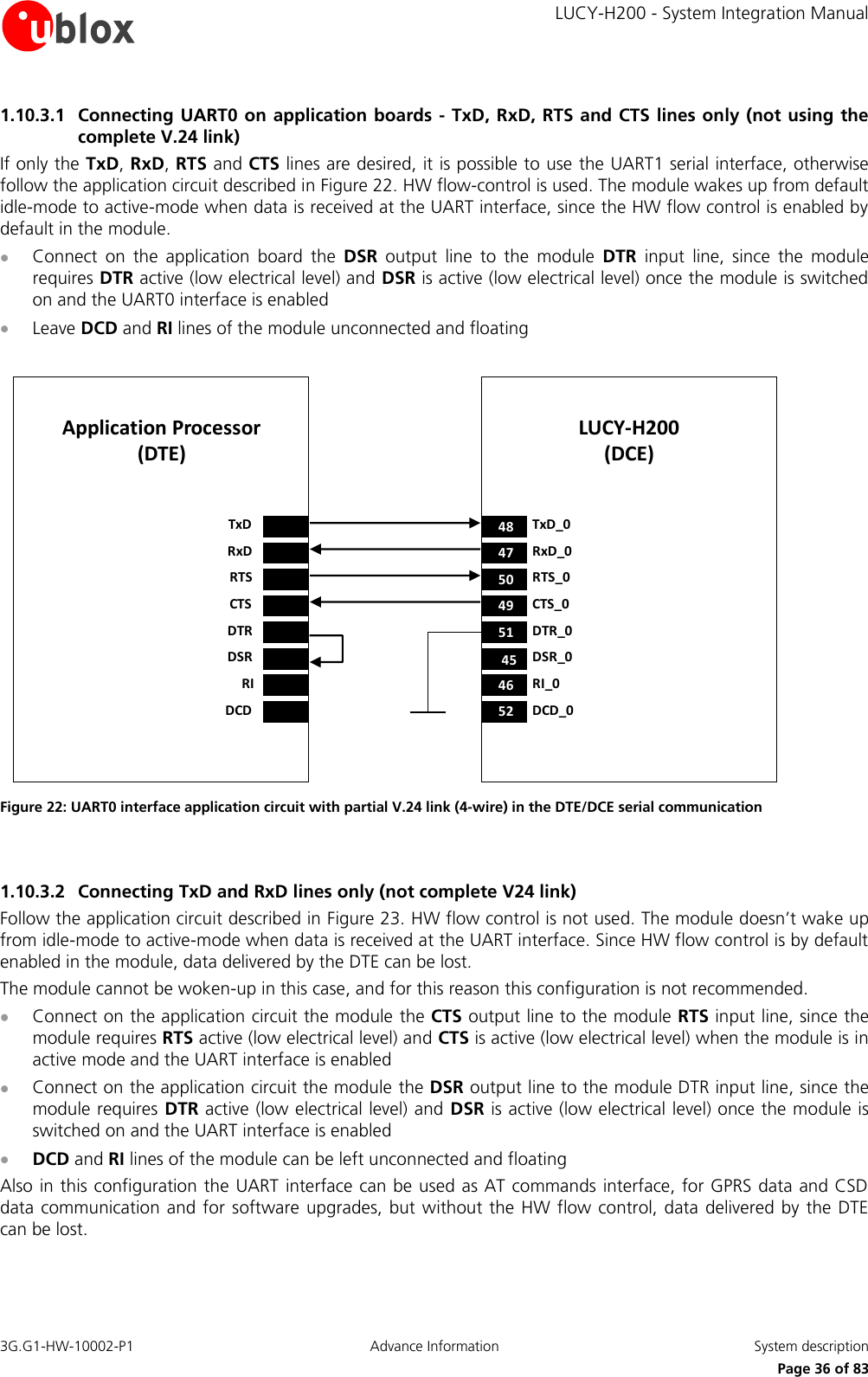
![LUCY-H200 - System Integration Manual 3G.G1-HW-10002-P1 Advance Information System description Page 35 of 83 Figure 19: RI behavior during incoming call The RI line is used to notify an SMS arrival. When the SMS arrives, the RI line switches from OFF to ON for 1 s (see Figure 20). Figure 20: RI behavior at SMS arrival 1.10.3 Connecting UART0 on application boards - Full RS-232 Functionality For complete RS-232 functionality conforming to ITU Recommendation [3] in DTE/DCE serial communication, the complete UART0 interface of the module (DCE) must be connected to the DTE as described in Figure 21. LUCY-H200(DCE)Application Processor(DTE)4847TxD_0RxD_05049RTS_0CTS_052464551 DTR_0DSR_0RI_0DCD_0TxDRxDRTSCTSDTRDSRRIDCD Figure 21: Interface application circuit with complete V.24 link in DTE/DCE serial communication SMS arrives time [s] 0 RI ON RI OFF 1s SMS time [s] 0 RI ON RI OFF 1s 1stime [s]151050RI ONRI OFFCall incomes1stime [s]151050RI ONRI OFFCall incomes](https://usermanual.wiki/u-blox/LUCYH200.Users-manual/User-Guide-1320517-Page-35.png)
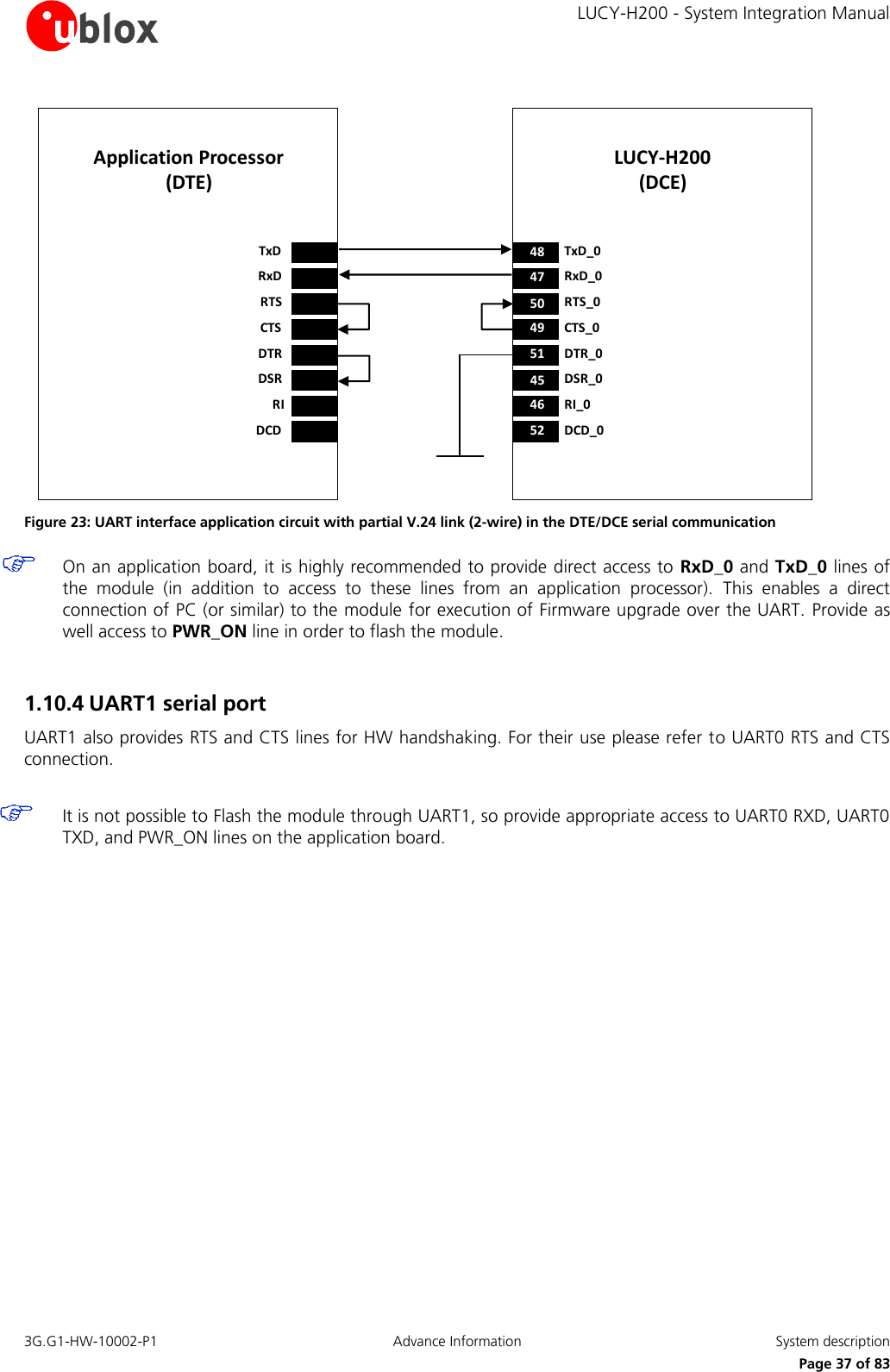
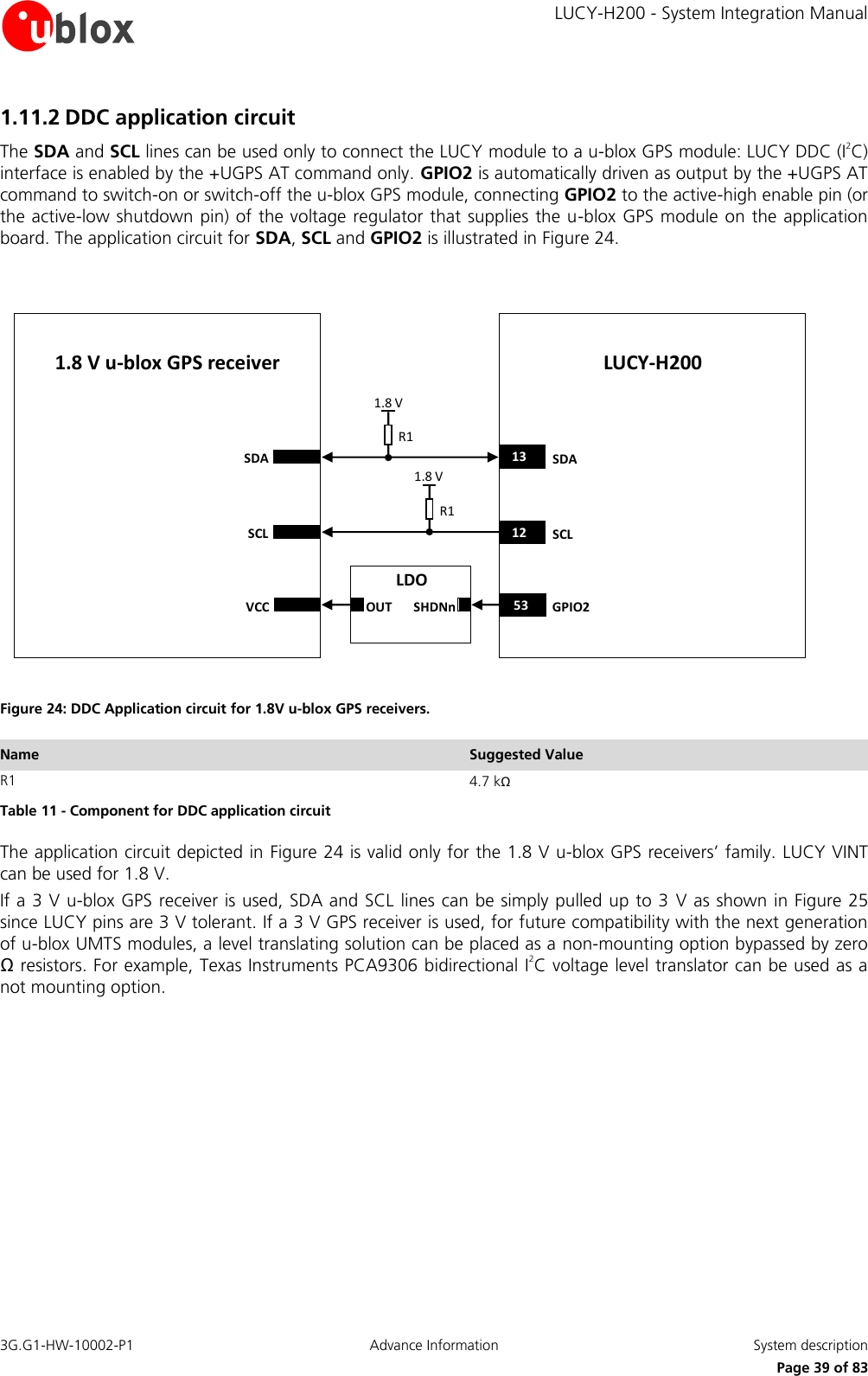
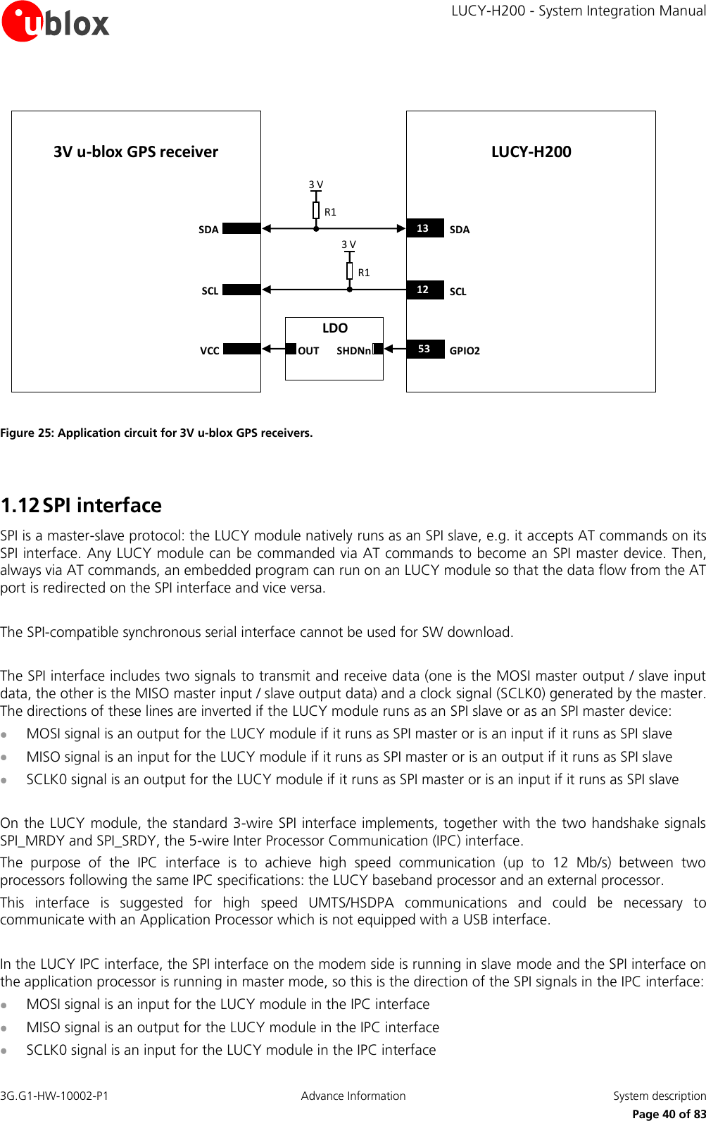
![LUCY-H200 - System Integration Manual 3G.G1-HW-10002-P1 Advance Information System description Page 38 of 83 1.10.5 MUX Protocol (3GPP 27.010) The module has a software layer with MUX functionality complaint with 3GPP 27.010 [8]. This is a data link protocol (layer 2 of OSI model) using HDLC-like framing and operates between the module (DCE) and the application processor (DTE). The protocol allows simultaneous sessions over the UART. Each session consists of a stream of bytes transferring various kinds of data like SMS, CBS, GPRS, AT commands in general. This permits, for example, SMS to be transferred to the DTE when a data connection is in progress. The following virtual channels are defined: Channel 0: control channel Channel 1 – 5: AT commands /data connection Channel 6: GPS tunnelling 1.11 DDC (I2C) interface 1.11.1 Overview An I2C compatible Display Data Channel (DDC) interface for serial communication is implemented. This interface is intended exclusively to access u-blox GPS receivers. Name Description Remarks SCL I2C bus clock line Open drain. External pull-up required. SDA I2C bus data line Open drain. External pull-up required. Table 10: DDC pins To be compliant to the I2C bus specifications, the module bus interface pads are open drain output and pull up resistors must be used. Since the pull-up resistors are not mounted on the module, they must be mounted externally. Resistor values must conform to the I2C bus specifications [7]. If the LUCY-H200 module is connected through the DDC bus to a single u-blox GPS receiver only (only one device is connected on the DDC bus), use a pull-up resistor of 4.7 k . Pull-ups must be connected to a supply voltage of 1.8 V (typical), since this is the voltage domain of the DDC pins. VINT voltage domain can be used to provide 1.8 V for the pull-ups (for detailed electrical characteristics see the LUCY-H200 Data Sheet [1]). DDC Slave-mode operation is not supported, the module can act as master only. Two lines, serial data (SDA) and serial clock (SCL), carry information on the bus. SCL is used to synchronize data transfers, and SDA is the data line. Since both lines are open drain outputs, the DDC devices can only drive them low or leave them open. The pull-up resistor pulls the line up to the supply rail if no DDC device is pulling it down to GND. If the pull-ups are missing, SCL and SDA lines are undefined and the DDC bus will not work. The signal shape is defined by the values of the pull-up resistors and the bus capacitance. Long wires on the bus will increase the capacitance. If the bus capacitance is increased, use pull-up resistors with nominal resistance value lower than 4.7 k , to match the I2C bus specifications regarding rise and fall times of the signals [7]. Capacitance must be limited on the bus to match the I2C specifications: route connections as short as possible. If the pins are not used as DDC bus interface, they can be left unconnected.](https://usermanual.wiki/u-blox/LUCYH200.Users-manual/User-Guide-1320517-Page-38.png)
![LUCY-H200 - System Integration Manual 3G.G1-HW-10002-P1 Advance Information System description Page 42 of 83 Since the module acts as a USB device, the USB supply (5.0 V typ.) must be provided to VUSB_DET by the connected USB host. As pointed out in chapter 1.6.1 if VUSB_DET is at VUSB range and USB is active, UART0 is automatically disabled, so the two peripherals cannot be used simultaneously. Take care to provide the needed accessibility (by means of test points, connector etc.) to UART0_TX, UART0_RX, and PWR_ON pins in order to re-flash/update LUCY module. The module does not enter idle mode when USB voltage (typically 5 V) is detected at VUSB_DET pin. When the module is connected to another device via USB (e.g. a PC) the module does not go in idle mode. The power consumption will be the same of the active state. This current is not taken from the PC but to the module power supply. 1.14 Serial interfaces configuration Not all the serial communication are allowed in the same time. Via a dedicated AT command it's possible to set up the preferred configuration, to be chosen into the following list (for more details please refer to u-blox 3.5G HSDPA AT Commands Manual [2]): Variant UART0 UART1 USB SPI (slave) 0 AT interface (if USB is not connected; otherwise disabled) RX and TX signals for debug purposes AT interface (if connected) 1 RX and TX signals for debug purposes AT interface AT interface 2 AT interface (if USB is not connected; otherwise disabled) RX and TX signals for debug purposes AT interface (if connected) AT interface Table 13 - Serial interfaces configuration For UART0 and UART1 is intended the full signals configuration if not indicated differently. 1.15 ADC input One Analog to Digital Converter input is available (ADC1) and is configurable using a custom AT command (see u-blox 3.5G HSDPA AT Commands Manual [2]). The resolution of this converter is 12-bit with a single ended input range. Name Description Remarks ADC1 ADC input Resolution: 12 bits. Table 14: ADC pin The electrical behavior of the measurement circuit in voltage mode can be modeled by a circuit equivalent to that shown in Figure 26. This includes a resistor (Req), voltage source (Ueq), analog preamplifier (with typical gain G=0.5), and a digital amplifier (with typical gain gADC=2048 LSB/V).](https://usermanual.wiki/u-blox/LUCYH200.Users-manual/User-Guide-1320517-Page-42.png)
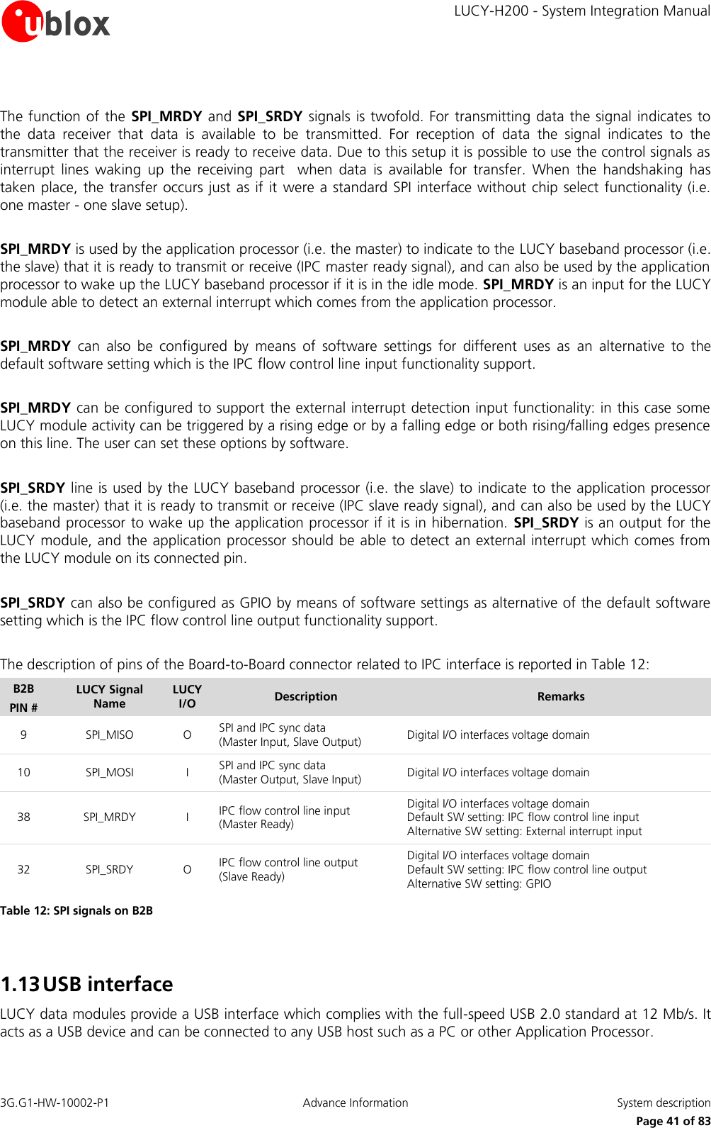
![LUCY-H200 - System Integration Manual 3G.G1-HW-10002-P1 Advance Information System description Page 43 of 83 LUCY-H200ADC1UeqReqUsigRsigUadcG27gADC Figure 26: Equivalent network for ADC single-ended measurement The ADC software driver takes care of the parameters shown in Figure 26 (Req, Ueq, G, gADC). The voltage measured by the ADC is Uadc. If the voltage source (Usig) has a significant internal resistance (Rsig) compared to the input resistance in measurement mode (Req) of the ADC, this should be taken into account and corrected. If an external voltage divider is implemented to increase the voltage range, check the input resistance in measurement mode (Req) of the ADC input and all the electrical characteristics. The detailed electrical specifications of the Analog to Digital Converter input are reported in the LUCY-H200 Data Sheet [1]. 1.16 General Purpose Input/Output (GPIO) The LUCY-H200 module provides five General Purpose Input/Output pins (GPIO1…GPIO5) which can be configured via u-blox AT commands (more details available in u-blox 3.5G HSDPA AT Commands Manual [2]). Some GPIOs are used for special indications as reported below: GPIO2 is dedicated for connection to a u-blox GPS receiver: AT commands are used to drive the GPIO as output to wake up the u-blox GPS module. If LUCY-H200 module is not connected to a u-blox GPS module, GPIO2 can be used for general purposes GPIO3 by default indicates whether the module is registered on a 2G or on a 3G network. If this indication is not needed, the GPIO can be used by means of the appropriate AT command GPIO4 by default indicates antenna jamming activity. If this indication is not needed, the GPIO can be used by means of the appropriate AT command When an LED is to be driven by means of a GPIO use a transistor and an appropriate voltage source as shown in the Figure 27 for GPIO1 and GPIO3. Use transistors with at least an integrated resistor in the base pin or otherwise put a 10 kΩ resistor on the board in series to the GPIO.](https://usermanual.wiki/u-blox/LUCYH200.Users-manual/User-Guide-1320517-Page-43.png)
![LUCY-H200 - System Integration Manual 3G.G1-HW-10002-P1 Advance Information System description Page 44 of 83 Figure 27: LED driving with GPIO Name Description Remarks T1 BCR135S BJT by Infineon Use transistors with at least an integrated resistor in the base pin or otherwise put a 10kΩ resistor on the board in series to the GPIO. Table 15 - Component for LED driving with GPIO 1.17 Audio Interface The LUCY-H200 module provides one digital and two analog audio interfaces: One microphone input One Speaker output I2S digital audio interface: input and output Audio signal routing can be controlled by the dedicated AT command +USPM (refer to u-blox 3.5G HSDPA AT Commands Manual [2]). This command allows setting the audio path mode, composed by the uplink audio path and the downlink audio path; e.g. in headset mode the uplink audio path is “Headset microphone”, the downlink audio path is “Mono headset”. In turns, each uplink path is composed by the audio input and by a set of parameters to process the audio signal (uplink gains, uplink digital filters, echo canceller parameters). For example “Headset microphone” uplink path uses the analog microphone input with a default analog gain of 27 dB. Each downlink path is composed by the audio output and by a set of parameters to process the audio signal (downlink gains, downlink digital filters, sidetone). These parameters can be changed with dedicated AT commands for each uplink or downlink path and then stored in 2 profiles in the non volatile memory (refer to u-blox 3.5G HSDPA AT Commands Manual [2] for Audio parameters tuning commands).](https://usermanual.wiki/u-blox/LUCYH200.Users-manual/User-Guide-1320517-Page-44.png)
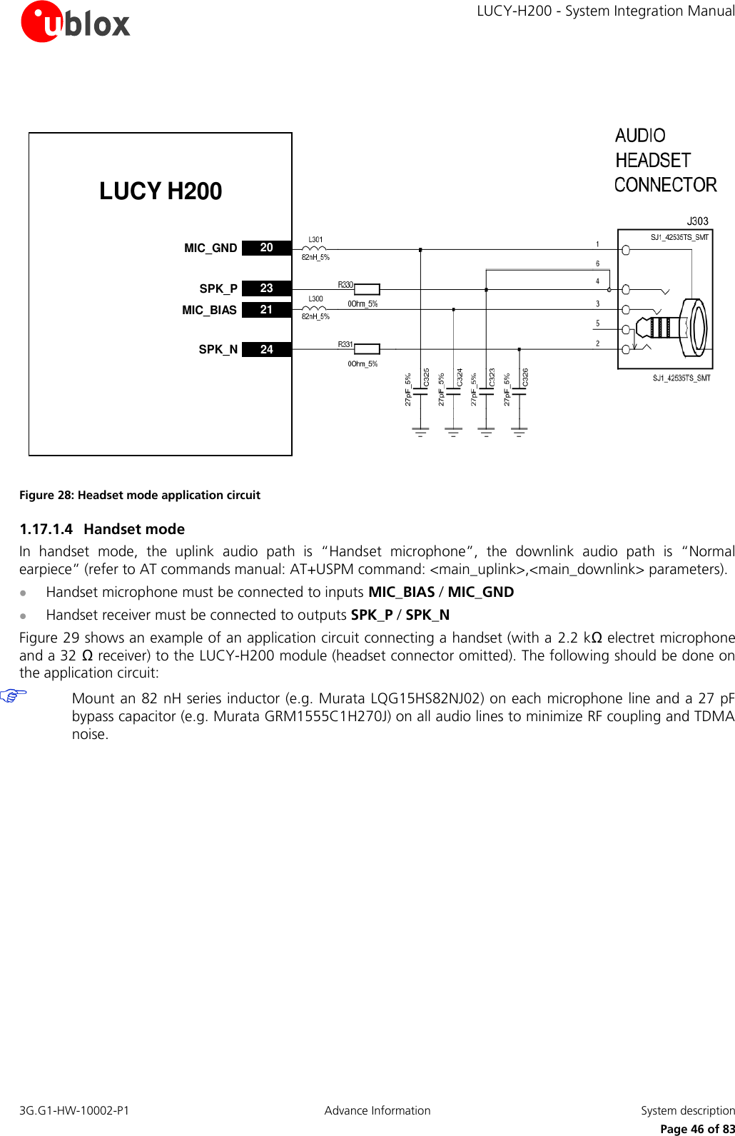
![LUCY-H200 - System Integration Manual 3G.G1-HW-10002-P1 Advance Information System description Page 45 of 83 1.17.1 Analog Audio interface 1.17.1.1 Microphone input The microphone input can be used for direct connection of the electret condenser microphone to a headset, handset or hands-free device. The main required electrical specifications for the electret condenser microphone are 2.2 k as maximum output impedance at 1 kHz and 2 V as maximum standard operating voltage. Board-to-board pins related to the microphone input are: MIC_BIAS: single ended supply to the microphone and represents the microphone signal input MIC_GND: local ground for the microphone Detailed electrical characteristics of the microphone input can be found in LUCY-H200 Data Sheet [1]. 1.17.1.2 Speaker output A differential high power audio output, can be used to directly connect a headset earpiece, handset earpiece or a loudspeaker used for ring-tones or for speech in a hands-free device. Board-to-board pins related to the speaker output are: SPK_N / SPK_P: high power differential audio output. These two pins are internally connected to the output of a high power differential audio amplifier Detailed electrical characteristics of the high power differential audio output can be found in LUCY-H200 Data Sheet [1]. Warning: excessive sound pressure from headphones can cause hearing loss. All audio lines on an Application Board must be routed in pairs, be embedded in GND (have the ground lines as close as possible to the audio lines), and maintain distance from noisy lines such as VCC and from components as switching regulators. 1.17.1.3 Headset mode Headset mode is the default audio operating mode of the LUCY-H200 module: In headset mode the uplink audio path is “Headset microphone”, the downlink audio path is “Mono headset” (refer to AT commands manual: AT+USPM command: <main_uplink>,<main_downlink> parameters) The audio path used in headset mode: Headset microphone must be connected to MIC_BIAS/MIC_GND Headset receiver must be connected to SPK_P/SPK_N Figure 28 shows an example of an application circuit connecting a headset (with a 2.2 kΩ electret microphone and a 32 Ω receiver) to the LUCY-H200 module (jack connector omitted). The following should be done on the application circuit: Mount an 82 nH series inductor (e.g. Murata LQG15HS82NJ02) on each microphone line, and a 27 pF bypass capacitor (e.g. Murata GRM1555C1H270J) on all audio lines to minimize RF coupling and TDMA noise.](https://usermanual.wiki/u-blox/LUCYH200.Users-manual/User-Guide-1320517-Page-45.png)
![LUCY-H200 - System Integration Manual 3G.G1-HW-10002-P1 Advance Information System description Page 47 of 83 LUCY-H200232021MIC_BIASMIC_GNDSPK_P24SPK_N Figure 29: Handset mode application circuit 1.17.1.5 Hands-free mode It is possible to implement a hands-free device using a loudspeaker and a microphone. In hands-free mode, the uplink audio path is “HF carkit microphone”, the downlink audio path is “Loudspeaker” (refer to AT commands manual: AT+USPM command: <main_uplink>, <main_downlink> parameters) .Hands-free functionality is implemented using appropriate DSP algorithms for voice band handling (echo canceller and automatic gain control), managed via software. (Refer to u-blox 3.5G HSDPA AT Commands Manual [2] - AT+UHFP command) Microphone must be connected to the input pins MIC_BIAS / MIC_GND High power loudspeaker must be connected to the output pins SPK_P / SPK_N The physical width of the high-power audio outputs lines on the application board must be wide enough to minimize series resistance. Figure 30 shows an application circuit for hands free mode. In this example the LUCY-H200 module is connected to an 8 Ω speaker and a 2.2 kΩ electret microphone. Insert an 82 nH series inductor (e.g. Murata LQG15HS82NJ02) on each microphone line and a 27 pF bypass capacitor (e.g. Murata GRM1555C1H270J) on all audio lines to minimize RF coupling and TDMA noise.](https://usermanual.wiki/u-blox/LUCYH200.Users-manual/User-Guide-1320517-Page-47.png)
![LUCY-H200 - System Integration Manual 3G.G1-HW-10002-P1 Advance Information System description Page 48 of 83 LUCY-H20020212324MIC_BIASMIC_GNDSPK_NSPK_P Figure 30: Hands-free mode application circuit 1.17.1.6 Connection to an external analog audio device When the LUCY-H200 module analog audio output is connected to an external audio device, SPK_P / SPK_N analog audio outputs can be used. A 10 µF series capacitor (e.g. Murata GRM188R60J106M) must be inserted between the SPK_P output and the single ended analog input of the external audio device (to decouple the bias). Audio devices with a differential analog input can be connected directly to SPK_P / SPK_N balanced output. The signal levels can be adapted by setting gain using AT commands, but additional circuitry must be inserted if the SPK_P / SPK_N output level of the module is too high for the input of the audio device. If the LUCY-H200 module analog audio input is connected to an external audio device, MIC_BIAS / MIC_GND can be used (default analog audio input of the module). Insert a 10 µF series capacitor (e.g. Murata GRM188R60J106M) between the single ended analog output of the external audio device and MIC_BIAS. Connect the reference of the single ended analog output of the external audio device to MIC_GND. If the external audio device is provided with a differential analog output, insert an additional differential to single ended circuit. The signal levels can be adapted by setting gain using AT commands, but additional circuitry must be inserted if the output level of the audio device is too high for MIC_BIAS. To enable the audio path corresponding to these input/output, please refer to u-blox 3.5G HSDPA AT Commands Manual [2]: AT+USPM command. To tune audio levels for the external device please refer to u-blox 3.5G HSDPA AT Commands Manual [2] (AT+USGC, AT+UMGC commands).](https://usermanual.wiki/u-blox/LUCYH200.Users-manual/User-Guide-1320517-Page-48.png)
![LUCY-H200 - System Integration Manual 3G.G1-HW-10002-P1 Advance Information System description Page 49 of 83 1.17.2 Digital mode / digital audio interface The LUCY-H200 module supports a bidirectional 4-wire I2S digital audio interface. The module acts as master only. The applicable pins are described in Table 16: Name Description Remarks I2S_WA I2S word alignment Module output (master) I2S_TXD I2S transmit data Module output I2S_CLK I2S clock Module output (master) I2S_RXD I2S receive data Module input Table 16: I2S interface pins The I2S interface can be can be used in two modes: PCM mode Normal I2S mode The I2S interface is activated and configured using AT commands, see u-blox 3.5G HSDPA AT Commands Manual: +USPM. Parameters of digital path can be configured and saved as the normal analog paths, using appropriate path index as described in the u-blox 3.5G HSDPA AT Commands Manual [2]. Analog gain parameters of microphone and speakers are unused when digital path is selected. I2S_TX and I2S_RX are respectively parallel to the analog front end, so resources available for analog path can be shared: Digital filters and digital gains are available in both uplink and downlink direction. Configure using AT commands Ringer tone and service tone are mixed on the TX path when active (downlink) The HF algorithm acts on I2S path Any external signal connected to the digital audio interface must be set low or tri-stated when the module is in power down mode to avoid an increase of module power consumption. If the external signals connected to the digital audio interface cannot be set low or tri-stated, insert a multi channel digital switch (e.g. Texas Instruments SN74CB3Q16244, TS5A3159, or TS5A63157) between the two-circuit connections and set to high impedance when the module is in power down mode. For debug purposes, include a test point at each I2S pin also if the digital audio interface is not used. Refer to the u-blox 3.5G HSDPA AT Commands Manual [2]: AT+UI2S command for possible combinations of connection and settings. 1.17.2.1 I2S interface - PCM mode Main features of the I2S interface in PCM mode: I2S runs in PCM - short alignment mode (configurable by AT commands) Module functions as I2S master (I2S_CLK and I2S_WA signals generated by the module) I2S_WA signal always runs at 8 kHz I2S_WA toggles high for 1 or 2 CLK cycles of synchronism (configurable), then toggles low for 16 CLK cycles of sample width. Frame length can be 1 + 16 = 17 bits or 2 + 16 = 18 bits I2S_CLK frequency depends on frame length. Can be 17 x 8 kHz = 136 kHz or 18 x 8 kHz = 144 kHz](https://usermanual.wiki/u-blox/LUCYH200.Users-manual/User-Guide-1320517-Page-49.png)
![LUCY-H200 - System Integration Manual 3G.G1-HW-10002-P1 Advance Information System description Page 50 of 83 I2S_TX, I2S_RX data are 16 bit words with 8 kHz sampling rate, mono. Data is in 2’s complement notation. MSB is transmitted first When I2S_WA toggles high, the first synchronization bit is always low. Second synchronization bit (present only in case of 2 bit long I2S_WA configuration) is MSB of the transmitted word (MSB is transmitted twice in this case) I2S_TX changes on I2S_CLK rising edge, I2S_RX changes on I2S_CLK falling edge 1.17.2.2 I2S interface - Normal I2S mode Normal I2S supports: 16 bits word mono interface 8 kHz frequency Main features of I2S interface in normal I2S mode: I2S_WA signal always runs at 8 kHz and synchronizes 2 channels (timeslots on WA high, WA low) I2S_TX data are composed of 16 bit words, dual mono (the words are written on both channels). Data are in 2’s complement notation. MSB is transmitted first. The bits are written on I2S_CLK rising or falling edge (configurable) I2S_RX data are read as 16 bit words, mono (words are read only on the timeslot with WA high). Data is read in 2’s complement notation. MSB is read first. The bits are read on the I2S_CLK edge opposite to I2S_TX writing edge (configurable) I2S_CLK frequency is 16 bits x 2 channels x 8 kHz = 256 kHz The modes are configurable through a specific AT command (refer to the related chapter in u-blox 3.5G HSDPA AT Commands Manual [2]) and the following parameters can be set: MSB can be 1 bit delayed or non-delayed on I2S_WA edge I2S_TX data can change on rising or falling edge of I2S_CLK signal (rising edge in this example) I2S_RX data are read on the opposite front of I2S_CLK signal 1.17.3 Voiceband processing system The voiceband processing on the LUCY-H200 is implemented in the DSP core inside the baseband chipset. The analog audio front-end of the chipset is connected to the digital system through 16 bit ADC converters in the uplink path, and through 16 bit DAC converters in the downlink path. External digital audio devices can be interfaced directly to the DSP digital processing part via the I2S digital interface. The analog amplifiers are skipped in this case. Possible processing of audio signal are: Speech encoding (uplink) and decoding (downlink).The following speech codecs are supported in firmware on the DSP: Fullrate, enhanced fullrate, and halfrate speech encoding and decoding Adaptive multi rate (fullrate and halfrate) speech encoding and decoding Mandatory sub-functions: Discontinuous transmission, DTX (GSM 46.031, 46.041, 46.081 and 46.093 standards) Voice activity detection, VAD (GSM 46.032, 46.042, 46.082 and 46.094 standards) Background noise calculation (GSM 46.012, 46.022, 46.062 and 46.092 standards) Signal routing: refer to the u-blox 3.5G HSDPA AT Commands Manual [2] (AT+USPM command)](https://usermanual.wiki/u-blox/LUCYH200.Users-manual/User-Guide-1320517-Page-50.png)
![LUCY-H200 - System Integration Manual 3G.G1-HW-10002-P1 Advance Information System description Page 51 of 83 Analog amplification, Digital amplification: please refer to the u-blox 3.5G HSDPA AT Commands Manual [2] (AT+USGC,+CLVL, +CRSL, +CMUT command) Digital filtering: please refer to the u-blox 3.5G HSDPA AT Commands Manual [2] (AT+UUBF, +UDBF commands) Hands-free algorithms (echo cancellation, Noise suppression, Automatic Gain control: refer to the u-blox 3.5G HSDPA AT Commands Manual [2] (AT+UHFP command) Sidetone generation (feedback of uplink speech signal to downlink path): please refer to the u-blox 3.5G HSDPA AT Commands Manual [2] (AT+USTN command) Playing/mixing of alert tones: Service tones: Tone generator with 3 sinus tones used (please refer to the u-blox 3.5G HSDPA AT Commands Manual [2]: AT+UPAR command) User generated tones: Tone generator with 3 sinus tones used (please refer to the u-blox 3.5G HSDPA AT Commands Manual [2]: AT+UTGN command) Midi melodies (for ringer): Synthesizer with up to 64 voices and a 48kHz sampling rate. (please refer to the u-blox 3.5G HSDPA AT Commands Manual [2]: AT+UPAR command) AMR files (for prompting): The storage format of AMR encoded audio content is defined in RFC3267 chapter 5 (please refer to the u-blox 3.5G HSDPA AT Commands Manual [2]: AT+UPLAYFILE command) With exception of the speech encoder/decoder, these audio processing can be controlled by AT commands. The block diagram in Figure 31 summarizes the voiceband audio processing in the DSP. Figure 31: Voiceband processing system block diagram](https://usermanual.wiki/u-blox/LUCYH200.Users-manual/User-Guide-1320517-Page-51.png)
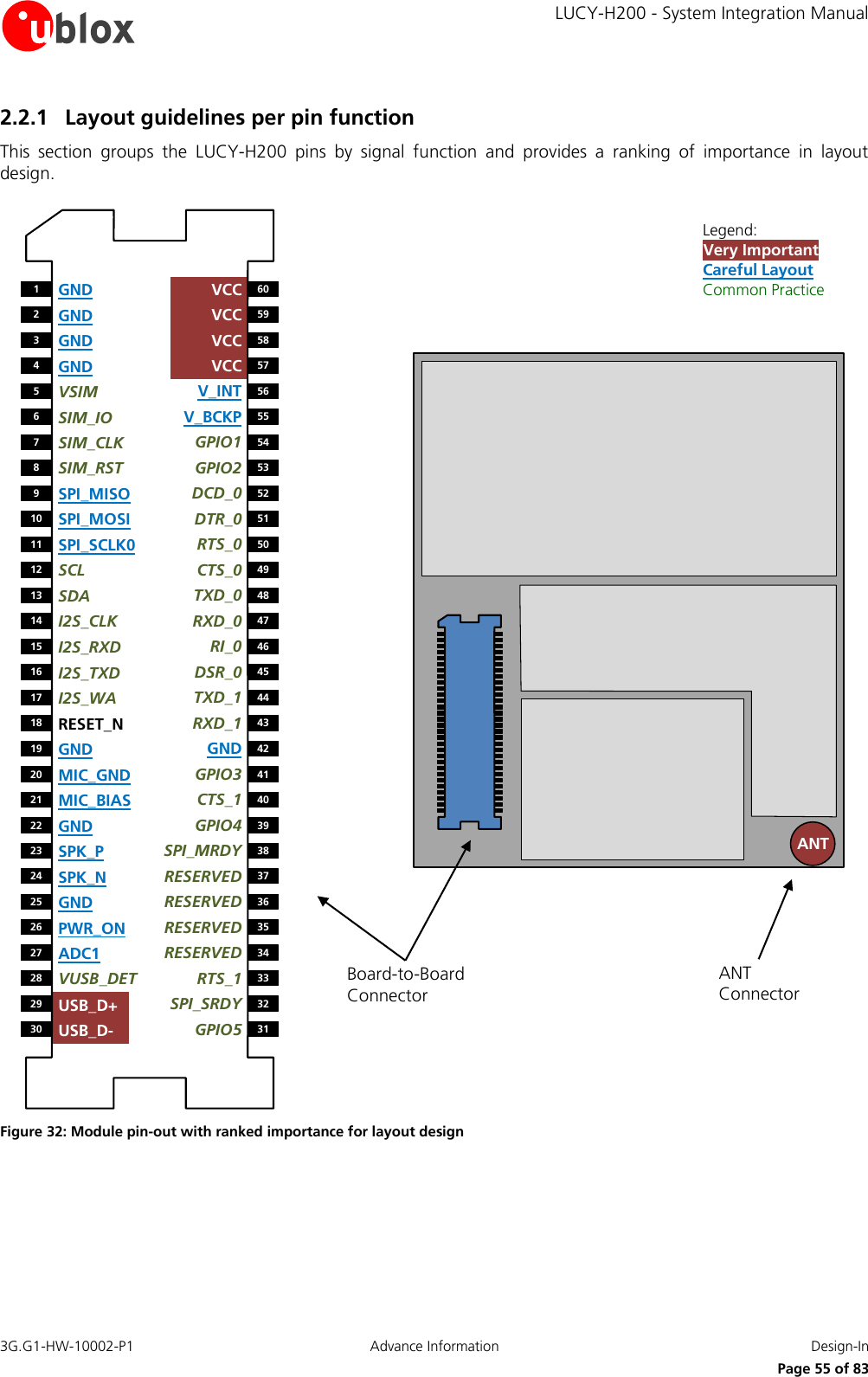
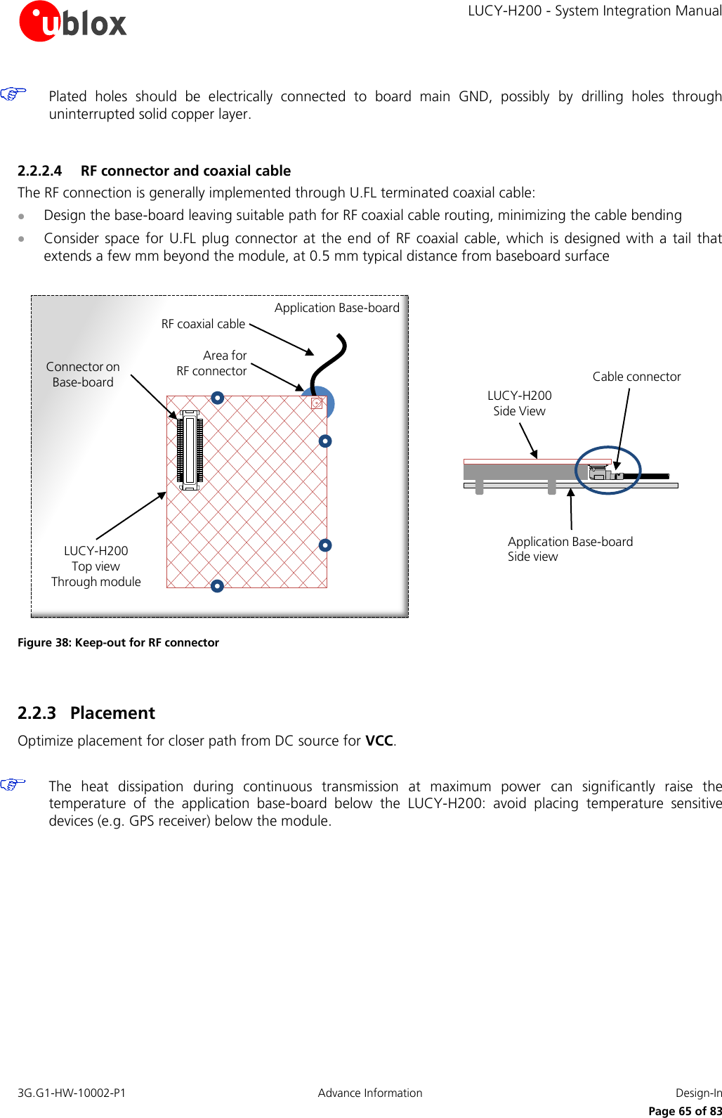
![LUCY-H200 - System Integration Manual 3G.G1-HW-10002-P1 Advance Information Design-In Page 62 of 83 2.2.2 Mechanical mating This section highlights mechanical aspects concerning the LUCY-H200 implementation on application base-board. The key factors to be considered for proper module mating is are as follows: Choose correct board-to-board connector. Consider module physical dimensions and implement keep-out area below module Design base-board for shielding cans solder tabs Leave space for RF antenna connector and coaxial cable 2.2.2.1 Board-to-board connector The board-to-board connector on the LUCY-H200 is MolexTM 052991-0608 or equivalent. The recommended mated connector for the customer’s application board is MolexTM 053748-0608 “0.50 mm Pitch 60-pin board-to-board connector (3 mm stacking mated height)”. Connector on LUCY-H200: MolexTM 052991-0608Connector on Application base-board:MolexTM 053748-0608 Figure 33: Board-to-board connector Follow the connector manufacturer’s recommendations for board-to-board foot-print: consider that misalignments in its placement will result in global misalignment on the whole module during installation on base-board. The exact geometry, distances, stencil thicknesses and solder paste volumes must be adapted to the specific production processes (e.g. soldering etc.) of the customer. 1.2 ±0.114.5 ±0.050.5 ±0.05 (pitch)2.2 ±0.11.2 ±0.10.25 (min)Dimensions in [mm] Figure 34: Board-to-board connector Footprint on Application base-board (according to MolexTM 053748-0608 datasheet)](https://usermanual.wiki/u-blox/LUCYH200.Users-manual/User-Guide-1320517-Page-62.png)
![LUCY-H200 - System Integration Manual 3G.G1-HW-10002-P1 Advance Information Design-In Page 63 of 83 2.2.2.2 Module keep-out Check the module dimensions on the LUCY-H200 Data Sheet [1] and leave suitable room on base-board PCB for module installation. Implement component “no placement” keep-out on the area below the module, the only component allowed is the mated board-to-board connector consider the extra clearance required for ergonomic handling of module during mating on the application baseboard: when manual installation is concerned, define non-placement area (e.g. 15x20 mm) for components with height greater than 2mm on two opposite sides of module PCB Routing below the LUCY-H200 on application motherboard is generally possible but not recommended. When installed on base-board, the LUCY-H200 shielding cans (connected to GND) may contact the top surface of application PCB with consequent risk of short to GND for unprotected signal routing on base-board top-layer Connector on Base-boardComponents keep-out below LUCY-H200on Base-boardApplication Base-boardArea for restrictions on components height (installation handling)37.5Dimensions in [mm]45.04.912.8 Figure 35: Keep-out dimensions 2.2.2.3 Shielding cans solder tabs There are four solder tabs for Pin-Through-Hole (PTH) soldering of the LUCY-H200 onto the application base-board. They are designed as part of the shielding cans, and therefore are electrically connected to module main Ground (GND).](https://usermanual.wiki/u-blox/LUCYH200.Users-manual/User-Guide-1320517-Page-63.png)
![LUCY-H200 - System Integration Manual 3G.G1-HW-10002-P1 Advance Information Design-In Page 64 of 83 4 x shielding cans solder tabs Figure 36: Tabs for Pin-through-Hole (PTH) soldering Proper installation and soldering tabs will ensure mechanical fixing of the LUCY-H200, will improve electromagnetic connection to GND and thermal heat-sink. The base-board needs to be designed with physical holes on coordinates corresponding to solder tabs, see Figure 37. Connector on Base-boardLUCY-H200Top view Through module4 x Soldering pads :Ø 3.0 Copper padØ 1.5 Plated holesApplication Base-board31.95 Dimensions in [mm]31.556.9512.1522.20 2.25 Figure 37: Coordinates of Plated Holes (PTH) on baseboard, for shields solder tabs The recommended soldering pads on application base-board have round copper pad, diameter = 3.0 mm, solder mask defined plated through hole, drill diameter = 1.5 mm Oblong holes are also acceptable, leading to better solder joint but more critical alignment of solder tabs to oblong holes during installation of module onto baseboard.](https://usermanual.wiki/u-blox/LUCYH200.Users-manual/User-Guide-1320517-Page-64.png)
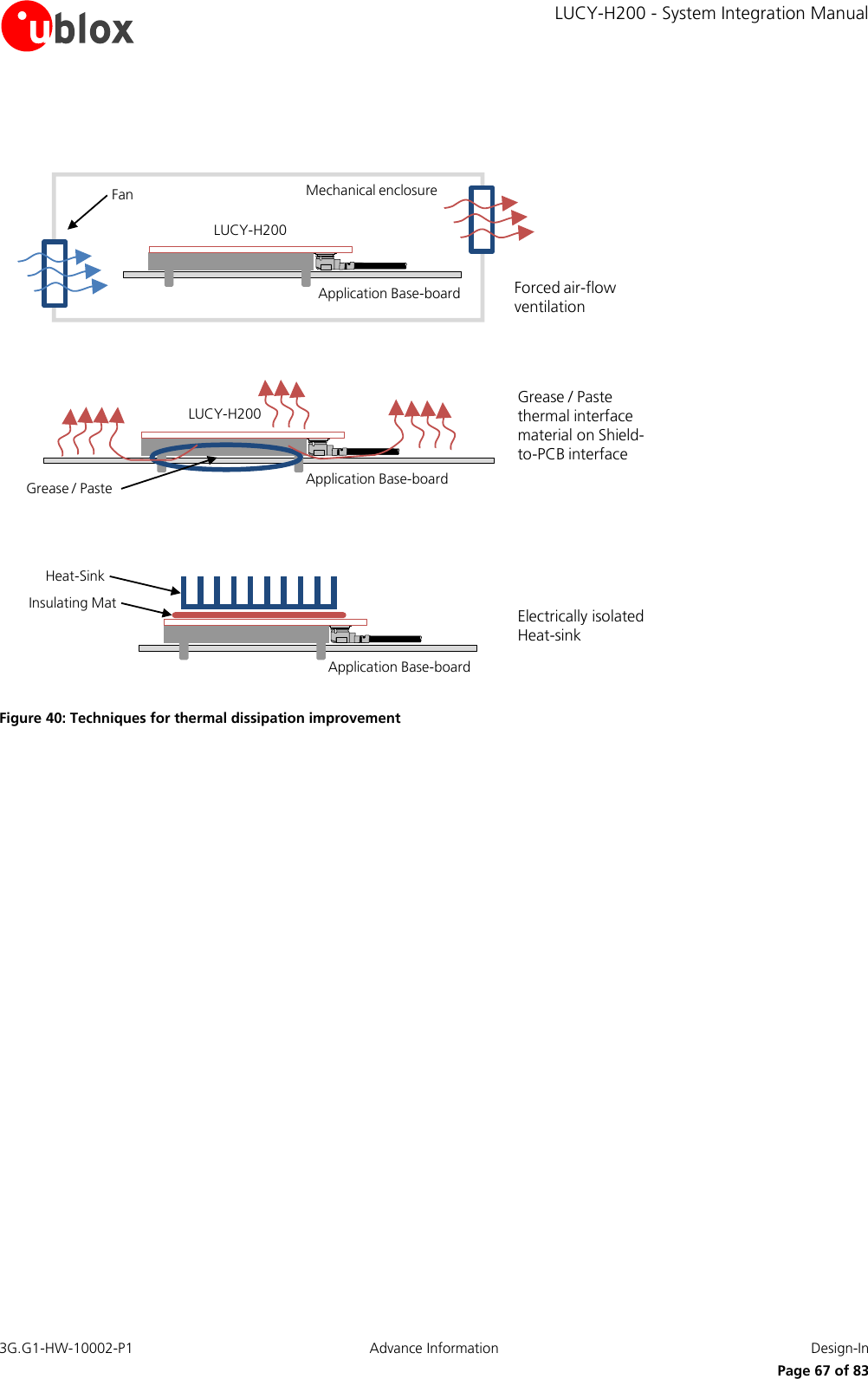
![LUCY-H200 - System Integration Manual 3G.G1-HW-10002-P1 Advance Information Design-In Page 66 of 83 LUCY-H200Application Base-boardTemperature-sensitive deviceLUCY-H200Application Base-boardTemperature-sensitive device(s)WrongCorrect Figure 39: Avoid placement of temperature sensitive devices below module 2.3 Thermal aspects The operating temperature range is declared on LUCY-H200 Data Sheet [1]. The most critical condition concerning thermal performances is the uplink transmission at the maximum power (data upload or voice call in connected mode), when the baseband processor runs at full speed, radio circuits are all active and the RF power amplifier is driven to higher output RF power. This scenario is not often encountered in real live network; however the application should be correctly designed to cope with it. During transmission on the maximum RF power the LUCY-H200 module generates heat power that may exceed 2 W: this is as indicative level, being the exact generated power strictly dependent of operating condition as the number of allocated TX slot and modulation (GMSK or 8PSK) or data rate (WCDMA), transmitting frequency band, etc. The generated thermal power must be adequately dissipated through the thermal and mechanical design of application. The Case-to-Ambient thermal resistance (RC-A) of the module, with the LUCY-H200 mounted on a 130 x 110 x 1.6 mm FR4 PCB with a high coverage of copper in still air conditions is approximately 15°C/W. With this Case-to-Ambient thermal resistance, the increasing of the module temperature is: around 10°C during a voice call at maximum power 20°C during EDGE data transfer with 4 TX slots up to 30°C in UMTS connection at max TX power Case-to-Ambient thermal resistance value will be different for other mechanical deployments of the module, e.g. PCB with different size and characteristics, mechanical shells enclosure, or forced air flow. The increasing of the thermal dissipation, i.e. reducing the thermal resistance, will reduce the operating temperature for internal circuitry of the LUCY-H200 for the same operating ambient temperature. This will improve the device long-term reliability for applications operating at high ambient temperature, e.g. greater than 55°C. Few techniques may be used to reduce the thermal resistance in the application (Figure 40): Forced ventilation air-flow within mechanical enclosure Usage of thermal transfer material (e.g. greases and pastes) as interposer between module shielding cans and application base-board, designed with no solder-mask on top layer for better thermal transfer Heat sink attached on module top side, with electrically insulated / high thermal conductivity adhesive](https://usermanual.wiki/u-blox/LUCYH200.Users-manual/User-Guide-1320517-Page-66.png)
![LUCY-H200 - System Integration Manual 3G.G1-HW-10002-P1 Advance Information Design-In Page 72 of 83 2.4.3 Antenna detection functionality The internal antenna detect circuit is based on ADC measurement at ANT: the RF port is DC coupled to the ADC unit in the baseband chip which injects a DC current (60 µA) on ANT and measures the resulting DC voltage to evaluate the resistance from ANT pad to GND. The antenna detection is forced by the +UANTR AT command: refer to the u-blox 3.5G HSDPA AT Commands Manual [2] for more details on how to access this feature. To achieve antenna detection functionality, use an RF antenna with built-in resistor from ANT signal to GND, or implement an equivalent solution with a circuit between the antenna cable connection and the radiating element as shown in Figure 45. Application Board Antenna AssemblyDiagnostic CircuitLUCY-H200ADCCurrent SourceRF ChokeDC BlockingFront-End RF ModuleRF ChokeDC BlockingRadiating ElementZo=50 ΩResistor for DiagnosticCoaxial Antenna CableANT Figure 45: Antenna detection circuit Description Part Number - Manufacturer DC Blocking Capacitor Murata GRM1555C1H220JA01 or equivalent RF Choke Inductor Murata LQG15HS68NJ02, LQG15HH68NJ02 or equivalent (Self Resonance Frequency ~1GHz) Resistor for Diagnostic 10kΩ 5%, various Manufacturers Table 19: Example of components for the antenna detection diagnostic circuit Please note that the DC impedance at RF port for some antennas may be a DC open (e.g. linear monopole) or a DC short to reference GND (e.g. PIFA antenna). For those antennas, without the diagnostic circuit of Figure 45 the measured DC resistance will always be at the limits of the measurement range (respectively open or short), and there will be no mean to distinguish between a defect on antenna path with similar characteristics (respectively: removal of linear antenna or RF cable shorted to GND for PIFA antenna).](https://usermanual.wiki/u-blox/LUCYH200.Users-manual/User-Guide-1320517-Page-72.png)
![LUCY-H200 - System Integration Manual 3G.G1-HW-10002-P1 Advance Information Design-In Page 73 of 83 It is recommended to use an antenna with a built-in diagnostic resistor in the range from 5 kΩ to 30 kΩ to assure good antenna detection functionality and to avoid a reduction of module RF performances. The choke inductor should exhibit a parallel Self Resonance Frequency (SRF) in the range of 1 GHz to improve the RF isolation of load resistor. For example: Consider a GSM antenna with built-in DC load resistor of 10 kΩ. Using the +UANTR AT command, the module reports the resistance value evaluated from ANT connector to GND: Reported values close to the used diagnostic resistor nominal value (i.e. values from 8 kΩ to 12 kΩ if a 10 kΩ diagnostic resistor is used) indicate that the antenna is properly connected Values close to the measurement range maximum limit (approximately 40 kΩ) or an open-circuit “over range” report (see u-blox 3.5G HSDPA AT Commands Manual [2]) means that that the antenna is not connected or the RF cable is broken open Reported values below the measurement range minimum limit (1 kΩ) will highlight a short to GND at antenna or along the RF cable Measurement inside the valid measurement range and outside the expected range may indicate an improper connection, damaged antenna or wrong value of antenna load resistor for diagnostic](https://usermanual.wiki/u-blox/LUCYH200.Users-manual/User-Guide-1320517-Page-73.png)
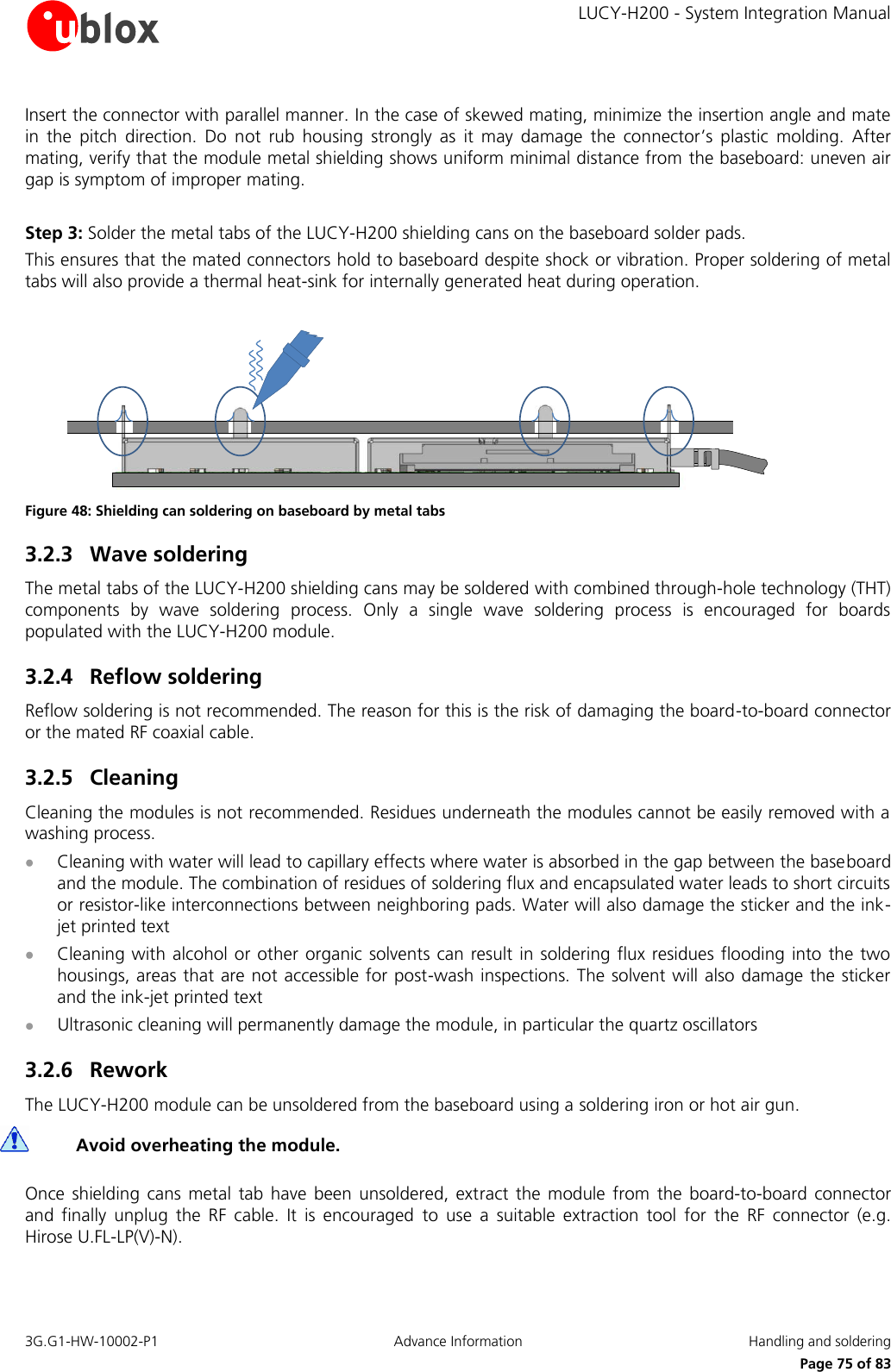
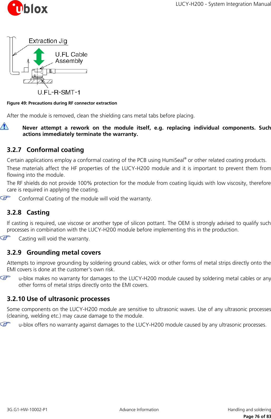
![LUCY-H200 - System Integration Manual 3G.G1-HW-10002-P1 Advance Information Handling and soldering Page 74 of 83 3 Handling and soldering 3.1 Packaging, shipping, storage and moisture preconditioning For information pertaining to reels and tapes, Moisture Sensitivity levels (MSD), shipment and storage information, as well as drying for preconditioning see the LUCY-H200 Data Sheet [1]. 3.2 Processing 3.2.1 ESD Hazard The LUCY-H200 is an Electro-Static Discharge (ESD) sensitive device. Ensure ESD precautions are implemented during handling of the module. 3.2.2 Hand soldering Hand soldering is the preferred method for mounting the LUCY-H200 on the baseboard. The procedure can be divided in following steps: Step1: Plug the RF coaxial cable on the LUCY-H200 U.FL receptacle to provide ANT connection. To mate the connectors, the mating axes of both connectors must be aligned and the connectors can be mated. The "click" will confirm fully mated connection. Do not attempt to insert on an extreme angle. Correct Wrong Figure 46: Precautions during RF connector mating Step 2: Mate the board-to-board connector on baseboard soldered receptacle. Follow precautions for mating from board-to-board connector manufacturer (see Figure 47). Correct Minimize angle Wrong Figure 47: Precautions during board-to-board mating and extraction](https://usermanual.wiki/u-blox/LUCYH200.Users-manual/User-Guide-1320517-Page-74.png)
![LUCY-H200 - System Integration Manual 3G.G1-HW-10002-P1 Advance Information Appendix Page 78 of 83 Appendix A Extra Features A.1 Firmware (upgrade) Over AT (FOAT) Firmware upgrade is available with LUCY modules using AT commands. A.1.1 Overview This feature allows upgrade the module Firmware over UART, using AT Commands. AT Command AT+UFWUPD triggers a reboot and followed by upgrade procedure at specified baud rate (refer to u-blox 3.5G HSDPA AT Commands Manual [2] for more details) The Xmodem-1k protocol is used for downloading the new Firmware image via a terminal application A special boot loader on the module performs Firmware installation, security verifications and module reboot Firmware authenticity verification is performed via a security signature during the download. Firmware is then installed, overwriting the current version. In case of power loss during this phase, the boot loader detects a fault at the next wake-up, and restarts the Firmware download from the Xmodem-1k handshake. After completing the upgrade, the module is reset again and wakes-up in normal boot A.1.2 FOAT procedure The application processor must proceed in the following way: send through the UART the AT+UFWUPD command, specifying the file type and the desired baud rate reconfigure the serial communication at the selected baud rate, without flow control with the Xmodem-1k protocol send the new FW image via Xmodem-1k A.2 Firewall The feature allows the LUCY-H200 user to reject incoming connections originated from IP addresses different from the specified list and inserted in a black list. A.3 TCP/IP Via the AT commands it’s possible to access the TCP/IP functionalities over the GPRS connection. For more details about AT commands see the u-blox 3.5G HSDPA AT Commands Manual [2]. A.3.1 Multiple IP addresses and sockets Using LUCY’s embedded TCP/IP or UDP/IP stack, only 1 IP instance (address) is supported. The IP instance supports up to 16 sockets. Using an external TCP/IP stack (on the application processor), it is possible to have 2 IP instances (addresses).](https://usermanual.wiki/u-blox/LUCYH200.Users-manual/User-Guide-1320517-Page-78.png)
![LUCY-H200 - System Integration Manual 3G.G1-HW-10002-P1 Advance Information Appendix Page 79 of 83 A.4 FTP The LUCY-H200 module supports via AT commands the File Transfer Protocol functionalities. File are read and stored in the local file system of the module. For more details about AT commands see the u-blox 3.5G HSDPA AT Commands Manual [2]. A.5 FTPS TBD A.6 HTTP HTTP client is implemented in LUCY. HEAD, GET, POST, DELETE and PUT operations are available. The file size to be uploaded / downloaded depends on the free space available in the local file system (FFS) at the moment of the operation. Up to 4 HTTP client contexts to be used simultaneously. For more details about AT commands see the u-blox 3.5G HSDPA AT Commands Manual [2]. A.7 HTTPS TBD. A.8 SMTP The LUCY-H200 module supports SMTP client functionalities. It is possible to specify the common parameters (e.g. server data, authentication method, etc.) can be specified, to send an email to a SMTP server. E-mails can be send with or without attachment. Attachments are store in the local file system of LUCY. For more details about AT commands see the u-blox 3.5G HSDPA AT Commands Manual [2]. A.9 GPS The LUCY-H200 module allows a simple and fast connection with the u-blox GPS modules (u-blox 5 family and above). Via the DDC bus it’s possible to communicate and exchange data, while the available GPIOs can handle the GPS device power on/off.](https://usermanual.wiki/u-blox/LUCYH200.Users-manual/User-Guide-1320517-Page-79.png)
![LUCY-H200 - System Integration Manual 3G.G1-HW-10002-P1 Advance Information Related documents Page 82 of 83 Related documents [1] u-blox LUCY-H200 Data Sheet, Document No 3G.G1-HW-10001 [2] u-blox 3.5G HSDPA AT Commands Manual, Docu. No 3G.G1-SW-10000 [3] ITU-T Recommendation V.24, 02-2000. List of definitions for interchange circuits between data terminal equipment (DTE) and data circuit-terminating equipment (DCE). http://www.itu.int/rec/T-REC-V.24-200002-I/en [4] 3GPP TS 27.007 - AT command set for User Equipment (UE) (Release 1999) [5] 3GPP TS 27.005 - Use of Data Terminal Equipment - Data Circuit terminating; Equipment (DTE - DCE) interface for Short Message Service (SMS) and Cell Broadcast Service (CBS) (Release 1999) [6] 3GPP TS 27.010 - Terminal Equipment to User Equipment (TE-UE) multiplexer protocol (Release 1999) [7] I2C-Bus Specification Version 2.1 Philips Semiconductors (January 2000) [8] 3GPP TS 27.010 - Terminal Equipment to User Equipment (TE-UE) multiplexer protocol (Release 1999) Part of the documents mentioned above can be downloaded from u-blox web-site (http://www.u-blox.com). Revision history Revision Date Name Status / Comments - 16/04/2010 lpah Initial Release P1 14/05/2010 lpah Chapter 1.18 fulfilled](https://usermanual.wiki/u-blox/LUCYH200.Users-manual/User-Guide-1320517-Page-82.png)