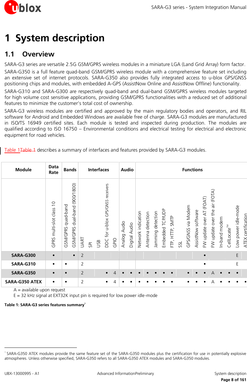
u blox SARAG350 Quad band (GSM850, GSM 900, DCS 1800, PCS 1900) GSM/GPRS transmitter module. User Manual SARA G3 series
u-blox AG Quad band (GSM850, GSM 900, DCS 1800, PCS 1900) GSM/GPRS transmitter module. SARA G3 series
u blox >
Contents
- 1. Users_manual
- 2. User manual
User manual
![SARA-G3 series - System Integration Manual UBX-13000995 - A1 Advanced InformationPreliminary System description Page 16 of 161 1.4 Operating modes SARA-G3 modules have several operating modes. The operating modes defined in Table 4Table 4 and described in detail in Table 5Table 5 provide general guidelines for operation. General Status Operating Mode Definition Power-down Not-Powered Mode VCC supply not present or below operating range: module is switched off. Power-Off Mode VCC supply within operating range and module is switched off. Normal Operation Idle-Mode Module processor core runs with 32 kHz reference, that is generated by: The internal 32 kHz oscillator (SARA-G350) The 32 kHz signal provided at the EXT32K pin (SARA-G300 and SARA-G310) Active-Mode Module processor core runs with 26 MHz reference generated by the internal oscillator. Connected-Mode Voice or data call enabled and processor core runs with 26 MHz reference. Table 4: Module operating modes definition Operating Mode Description Transition between operating modes Not-Powered Mode Module is switched off. Application interfaces are not accessible. Internal RTC timer operates on SARA-G350 modules only if a valid voltage is applied to V_BCKP pin. Additionally, a proper external 32 kHz signal must be fed to EXT32K pin on SARA-G300 / SARA-G310 to let RTC timer running that otherwise is not in operation. When VCC supply is removed, the module enters not-powered mode. When in not-powered mode, the module cannot be switched on by a low level on PWR_ON input or by a preset RTC alarm. When in not-powered mode, the module can be switched on applying VCC supply (refer to 2.2.1) so that the module switches from not-powered to active-mode. Power-Off Mode Module is switched off: normal shutdown by an appropriate power-off event (refer to 1.6.2). Application interfaces are not accessible. Internal RTC timer operates on SARA-G350 modules. A proper external 32 kHz signal must be fed to the EXT32K pin on SARA-G300 / SARA-G310 to let RTC timer running that otherwise is not in operation. When the module is switched off by an appropriate power-off event (refer to 1.6.2), the module enters power-off mode from active-mode. When in power-off mode, the module can be switched on by a low level on PWR_ON input or by a preset RTC alarm (refer to 2.2.1): module switches from power-off to active-mode. When VCC supply is removed, the module switches from power-off mode to not-powered mode. Idle-Mode The module is not ready to communicate with an external device by means of the application interfaces since configured to reduce power consumption. The module automatically enters idle-mode whenever possible if power saving is enabled by the AT+UPSV command (refer to u-blox AT Commands Manual [2]), reducing power consumption (refer to 1.5.1.3). The CTS output line indicates when the UART interface is disabled/enabled due to the module idle/active-mode according to power saving and hardware flow control settings (refer to 1.9.1.3, 1.9.1.4). Power saving configuration is not enabled by default: it can be enabled by the AT+UPSV command (see u-blox AT Commands Manual [2]). A proper 32 kHz signal must be fed to the EXT32K pin of SARA-G300 and SARA-G310 modules to let idle-mode that otherwise cannot be reached (this is not needed for the other SARA-G3 series modules). The module automatically switches from active-mode to idle-mode whenever possible if power saving is enabled (refer to sections 1.5.1.3, 1.9.1.4 and to the u-blox AT Commands Manual [2], AT+UPSV). The module wakes up from idle-mode to active-mode in the following events: Automatic periodic monitoring of the paging channel for the paging block reception according to network conditions (refer to 1.5.1.3, 1.9.1.4) Automatic periodic enable of the UART interface to receive and send data, if the power saving AT command is set to 1 (refer to 1.9.1.4) RTC alarm occurs (refer to u-blox AT Commands Manual [2], AT+CALA command) Data received on UART interface (refer to 1.9.1.4) RTS input line set to the ON state by the DTE if hardware flow control has been disabled by AT&K3 and the power saving AT command is set to 2 (refer to 1.9.1.4) GPS data ready: when the GPIO3 pin is informed by the connected u-blox GPS/GNSS receiver that it is ready to send data via the DDC (I2C) interface (refer to 1.11, 1.9.3)](https://usermanual.wiki/u-blox/SARAG350.User-manual/User-Guide-2055502-Page-16.png)
![SARA-G3 series - System Integration Manual UBX-13000995 - A1 Advanced InformationPreliminary System description Page 17 of 161 Operating Mode Description Transition between operating modes Active-Mode The module is ready to communicate with an external device by means of the application interfaces unless power saving configuration is enabled by the AT+UPSV command (refer to sections 1.5.1.3, 1.9.1.4 and to the u-blox AT Commands Manual [2]). When the module is switched on by an appropriate power-on event (refer to 2.2.1), the module enters active-mode from not-powered or power-off mode. If power saving configuration is enabled by the AT+UPSV command, the module automatically switches from active to idle-mode whenever possible and the module wakes up from idle to active-mode in the events listed above (refer to idle to active transition description). When a voice call or a data call is initiated, the module switches from active-mode to connected-mode. Connected-Mode A voice call or a data call is in progress. The module is ready to communicate with an external device by means of the application interfaces unless power saving configuration is enabled by the AT+UPSV command (see sections 1.5.1.3, 1.9.1.4 and the u-blox AT Commands Manual [2][2]). When a voice call or a data call is initiated, the module enters connected-mode from active-mode. When a voice call or a data call is terminated, the module returns to the active-mode. Table 5: Module operating modes description Figure 3Figure 3 describes the transition between the different operating modes. Switch ON:•Apply VCCIf power saving is enabled and there is no activity for a defined time intervalAny wake up event described in the module operating modes summary table aboveIncoming/outgoing call or other dedicated device network communicationCall terminated, communication droppedRemove VCCSwitch ON:•PWR_ON•RTC AlarmNot poweredPower offActiveConnected IdleSwitch OFF:•AT+CPWROFF Figure 3: Operating modes transition](https://usermanual.wiki/u-blox/SARAG350.User-manual/User-Guide-2055502-Page-17.png)
![SARA-G3 series - System Integration Manual UBX-13000995 - A1 Advanced InformationPreliminary System description Page 18 of 161 1.5 Supply interfaces 1.5.1 Module supply input (VCC) SARA-G3 modules must be supplied via the three VCC pins that represent the module power supply input. The VCC pins are internally connected to the RF power amplifier and to the integrated Power Management Unit: all supply voltages needed by the module are generated from the VCC supply by integrated voltage regulators, including V_BCKP Real Time Clock supply, V_INT digital interfaces supply and VSIM SIM card supply. During operation, the current drawn by the SARA-G3 series modules through the VCC pins can vary by several orders of magnitude. This ranges from the high peak of current consumption during GSM transmitting bursts at maximum power level in connected-mode (as described in section 1.5.1.2), to the low current consumption during low power idle-mode with power saving enabled (as described in section 1.5.1.3). 1.5.1.1 VCC supply requirements Table 6Table 6 summarizes the requirements for the VCC module supply. Refer to section 2.1.1 for all the suggestions to properly design a VCC supply circuit compliant to the requirements listed in Table 6Table 6. The VCC supply circuit affects the RF compliance of the device integrating SARA-G3 series module with applicable required certification schemes as well as antenna circuit design. Compliance is guaranteed if the VCC requirements summarized in the Table 6Table 6 are fulfilled. Item Requirement Remark VCC nominal voltage Within VCC normal operating range: 3.35 V min. / 4.50 V max. The module cannot be switched on if VCC voltage value is below the normal operating range minimum limit. Ensure that the input voltage at VCC pins is above the minimum limit of the normal operating range for at least more than 3 s after the module switch-on. VCC voltage during normal operation Within VCC extended operating range: 3.00 V min. / 4.50 V max. The module may switch off when VCC voltage drops below the extended operating range minimum limit. Operation above extended operating range maximum limit is not recommended and exposure beyond it may affect device reliability. VCC average current Considerably withstand maximum average current consumption value in connected-mode conditions specified in SARA-G3 series Data Sheet [1][1]. The maximum average current consumption can be greater than the specified value according to the actual antenna mismatching, temperature and VCC voltage. Section 1.5.1.21.5.1.2 describes connected-mode current. VCC peak current Withstand the maximum peak current consumption specified in the SARA-G3 series Data Sheet [1][1]. The specified maximum peak of current consumption occurs during GSM single transmit slot in 850/900 MHz connected-mode, in case of mismatched antenna. Section 1.5.1.21.5.1.2 describes connected-mode current. VCC voltage drop during Tx slots Lower than 400 mV VCC voltage drop values greater than recommended during 2G TDMA transmission slots directly affect the RF compliance with applicable certification schemes. Figure 5Figure 5 describes VCC voltage drop during Tx slots. VCC voltage ripple during Tx slots Lower than 30 mVpp if fripple ≤ 200 kHz Lower than 10 mVpp if 200 kHz < fripple ≤ 400 kHz Lower than 2 mVpp if fripple > 400 kHz VCC voltage ripple values higher than recommended during 2G transmission directly affect the RF compliance with applicable certification schemes. Figure 5Figure 5 describes VCC voltage ripple during Tx slots. Formatted: Font: 8 ptField Code ChangedFormatted: Font: 8 pt, French(Canada)Formatted: Font: 8 ptField Code ChangedFormatted: Font: 8 pt, French(Canada)Formatted: Font: 8 ptFormatted: Font: 8 pt](https://usermanual.wiki/u-blox/SARAG350.User-manual/User-Guide-2055502-Page-18.png)
![SARA-G3 series - System Integration Manual UBX-13000995 - A1 Advanced InformationPreliminary System description Page 19 of 161 Item Requirement Remark VCC under/over-shoot at start/end of Tx slots Absent or at least minimized VCC under/over-shoot higher than recommended at the start/end of 2G TDMA transmission slots directly affect the RF compliance with applicable certification schemes. Figure 5Figure 5 describes VCC voltage under/over-shoot at the start/end of Tx slots Table 6: Summary of VCC supply requirements For the additional specific requirement for SARA-G350 ATEX modules integration in potentially explosive atmospheres applications, refer to section 2.13. 1.5.1.2 VCC current consumption in connected-mode When a GSM call is established, the VCC consumption is determined by the current consumption profile typical of the GSM transmitting and receiving bursts. The current consumption peak during a transmission slot is strictly dependent on the transmitted power, which is regulated by the network. If the module is transmitting in GSM talk mode in the 850 or 900 MHz bands, at the maximum RF power control level (approximately 2 W or 33 dBm in the allocated transmit slot/burst) the current consumption can reach up to 1900 mA (with a highly unmatched antenna) for 576.9 µs (width of the transmit slot/burst) with a periodicity of 4.615 ms (width of 1 frame = 8 slots/burst), so with a 1/8 duty cycle according to GSM TDMA (Time Division Multiple Access). If the module is in GSM connected-mode in the 1800 or 1900 MHz bands, the current consumption figures are lower than the one in the 850 or 900 MHz bands, due to 3GPP transmitter output power specifications (refer to SARA-G3 series Data Sheet [1]). During a GSM call, current consumption is in the order of 60-120 mA in receiving or in monitor bursts and is about 10-40 mA in the inactive unused bursts (low current period). The more relevant contribution to determinefactor for determining the average current consumption, is set by the transmitted power in the transmit slot. Figure 4Figure 4 shows an example of the module current consumption profile versus time in GSM talk mode. Time [ms]RX slotunused slotunused slotTX slotunused slotunused slotMON slotunused slotRX slotunused slotunused slotTX slotunused slotunused slotMON slotunused slotGSM frame 4.615 ms (1 frame = 8 slots)Current [A]200 mA60-120 mA1900 mAPeak current depends on TX powerGSM frame 4.615 ms (1 frame = 8 slots)1.51.00.50.02.060-120 mA10-40 mA Figure 4: VCC current consumption profile versus time during a GSM call (1 TX slot, 1 RX slot) Formatted: Font: 8 pt](https://usermanual.wiki/u-blox/SARAG350.User-manual/User-Guide-2055502-Page-19.png)
![SARA-G3 series - System Integration Manual UBX-13000995 - A1 Advanced InformationPreliminary System description Page 20 of 161 Figure 5Figure 5 illustrates VCC voltage profile versus time during a GSM call, according to the relative VCC current consumption profile described in Figure 4Figure 4. TimeundershootovershootrippledropVoltage3.8 V (typ)RX slotunused slotunused slotTX slotunused slotunused slotMON slotunused slotRX slotunused slotunused slotTX slotunused slotunused slotMON slotunused slotGSM frame 4.615 ms (1 frame = 8 slots)GSM frame 4.615 ms (1 frame = 8 slots) Figure 5: Description of the VCC voltage profile versus time during a GSM call When a GPRS connection is established, more than one slot can be used to transmit and/or more than one slot can be used to receive. The transmitted power depends on network conditions, which set the peak current consumption, but following the GPRS specifications the maximum transmitted RF power is reduced if more than one slot is used to transmit, so the maximum peak of current is not as high as can be in case of a GSM call. If the module transmits in GPRS multi-slot class 10, in the 850 or 900 MHz bands, at the maximum power control level, the consumption can reach up to 1600 mA (with highly unmatched antenna). This happens for 1.154 ms (width of the 2 Tx slots/bursts) with a periodicity of 4.615 ms (width of 1 frame = 8 slots/bursts), so with a 1/4 duty cycle, according to GSM TDMA. If the module is in GPRS connected-mode in 1800 or 1900 MHz bands, consumption figures are lower than in the 850 or 900 MHz band, due to 3GPP Tx power specifications. Figure 6Figure 6 reports the current consumption profiles in GPRS connected-mode, in the 850 or 900 MHz bands, with 2 slots used to transmit and 1 slot used to receive. Time [ms]RX slotunused slotunused slotTX slotTX slotunused slotMON slotunused slotRX slotunused slotunused slotTX slotTX slotunused slotMON slotunused slotGSM frame 4.615 ms (1 frame = 8 slots)Current [A]60-120mAGSM frame 4.615 ms (1 frame = 8 slots)1.51.00.50.02.060-120mA 10-40mA200mAPeak current depends on TX power1600 mA Figure 6: VCC current consumption profile versus time during a GPRS connection (2 TX slots, 1 RX slot)](https://usermanual.wiki/u-blox/SARAG350.User-manual/User-Guide-2055502-Page-20.png)
![SARA-G3 series - System Integration Manual UBX-13000995 - A1 Advanced InformationPreliminary System description Page 21 of 161 1.5.1.3 VCC current consumption in cyclic idle/active-mode (power saving enabled) The power saving configuration is by default disabled, but it can be enabled using the appropriate AT command (refer to u-blox AT Commands Manual [2], AT+UPSV command). When power saving is enabled, the module automatically enters idle-mode whenever possible, reducing current consumption. During idle-mode, the module processor runs with 32 kHz reference clock frequency. For SARA-G350 modules, the internal oscillator automatically generates the 32 kHz clock. For SARA-G300 and SARA-G310 modules, a valid 32 kHz signal must be properly provided to the EXT32K input pin of the module to let idle-mode, that otherwise cannot be reached (this is not needed for the other SARA-G3 series modules). When power saving is enabled, the module is registered or attached to a network and a voice or data call is not enabled, the module automatically enters idle-mode whenever possible, but it must periodically monitor the paging channel of the current base station (paging block reception), in accordance to GSM system requirements. When the module monitors the paging channel, it wakes up to active-mode, to enable the reception of paging block. In between, the module switches to idle-mode. This is known as GSM discontinuous reception (DRX). The module processor core is activated during the paging block reception, and automatically switches its reference clock frequency from 32 kHz to the 26 MHz used in active-mode. The time period between two paging block receptions is defined by the network. This is the paging period parameter, fixed by the base station through broadcast channel sent to all users on the same serving cell. The time interval between two paging block receptions can be from 470.76 ms (DRX = 2, i.e. width of 2 GSM multiframes = 2 x 51 GSM frames = 2 x 51 x 4.615 ms) up to 2118.42 ms (DRX = 9, i.e. width of 9 GSM multiframes = 9 x 51 frames = 9 x 51 x 4.615 ms). Figure 7Figure 7 roughly describes the current consumption profile of SARA-G350 modules, or specifically of SARA-G300 / SARA-G310 modules when their EXT32K input pin is fed by an external 32 kHz signal with characteristics compliant to the one specified in SARA-G3 series Data Sheet [1], when power saving is enabled. The module is registered with the network, automatically enters the very low power idle-mode, and periodically wakes up to active-mode to monitor the paging channel for paging block reception. 20-30 msIDLE MODE ACTIVE MODE IDLE MODE300-600 µAActive Mode EnabledIdle Mode Enabled300-600 µA60-120 mA0.44-2.09 sIDLE MODE20-30 msACTIVE MODETime [s]Current [mA]100500Time [ms]Current [mA]1005004-5 mA60-120 mARX Enabled20-40 mADSP Enabled Figure 7: VCC current consumption profile versus time of the SARA-G350 modules or the SARA-G300 / SARA-G310 modules (with the EXT32K input fed by a proper external 32 kHz signal), when registered with the network, with power saving enabled: the very low power idle-mode is reached and periodical wake up to active-mode are performed to monitor the paging channel](https://usermanual.wiki/u-blox/SARAG350.User-manual/User-Guide-2055502-Page-21.png)
![SARA-G3 series - System Integration Manual UBX-13000995 - A1 Advanced InformationPreliminary System description Page 22 of 161 Figure 8Figure 8 roughly describes the current consumption profile of SARA-G300 / SARA-G310 modules when the EXT32K input pin is fed by the 32K_OUT output pin provided by these modules, when power saving is enabled. The module is registered with the network, automatically enters the low power idle-mode and periodically wakes up to active-mode to monitor the paging channel for paging block reception. 20-30 msIDLE MODE ACTIVE MODE IDLE MODE3-4 mAActive Mode EnabledIdle Mode Enabled3-4 mA60-120 mA0.44-2.09 sIDLE MODE20-30 msACTIVE MODETime [s]Current [mA]100500Time [ms]Current [mA]1005004-5 mA60-120 mARX Enabled20-40 mADSP Enabled Figure 8: VCC current consumption profile versus time of the SARA-G300 / SARA-G310 modules (with the EXT32K input pin fed by the 32K_OUT output pin provided by these modules), when registered with the network, with power saving enabled: the low power idle-mode is reached and periodical wake up to active-mode are performed to monitor the paging channel](https://usermanual.wiki/u-blox/SARAG350.User-manual/User-Guide-2055502-Page-22.png)
![SARA-G3 series - System Integration Manual UBX-13000995 - A1 Advanced InformationPreliminary System description Page 23 of 161 1.5.1.4 VCC current consumption in fixed active-mode (power saving disabled) Power saving configuration is by default disabled, or it can be disabled using the appropriate AT command (refer to u-blox AT Commands Manual [2], AT+UPSV command). When power saving is disabled, the module does not automatically enter idle-mode whenever possible: the module remains in active-mode. The module processor core is activated during active-mode, and the 26 MHz reference clock frequency is used. Figure 9Figure 9 roughly describes the current consumption profile of SARA-G300 / SARA-G310 modules when the EXT32K input pin is fed by external 32 kHz signal with characteristics compliant to the one specified in SARA-G3 series Data Sheet [1], or by the 32K_OUT output pin provided by these modules, when power saving is disabled. The module is registered with the network, active-mode is maintained, and the receiver and the DSP are periodically activated to monitor the paging channel for paging block reception. ACTIVE MODE60-120 mA0.47-2.12 sPaging periodTime [s]Current [mA]100500Time [ms]Current [mA]1005003-5 mA60-120 mARX Enabled20-40 mADSP Enabled3-5 mA3-5 mA Figure 9: VCC current consumption profile versus time of the SARA-G300 / SARA-G310 modules (with the EXT32K input pin fed by proper external 32 kHz signal or by 32K_OUT output pin), when registered with the network, with power saving disabled: the active-mode is always held, and the receiver and the DSP are periodically activated to monitor the paging channel](https://usermanual.wiki/u-blox/SARAG350.User-manual/User-Guide-2055502-Page-23.png)
![SARA-G3 series - System Integration Manual UBX-13000995 - A1 Advanced InformationPreliminary System description Page 24 of 161 Figure 10Figure 10 roughly describes the current consumption profile of SARA-G350 modules or the current consumption profile of SARA-G300 / SARA-G310 modules when their EXT32K input is not fed by a signal (left unconnected), when power saving is disabled: the module is registered with the network, active-mode is maintained, and the receiver and the DSP are periodically activated to monitor the paging channel for paging block reception. ACTIVE MODE15-18 mA60-120 mA0.47-2.12 sPaging periodTime [s]Current [mA]100500Time [ms]Current [mA]10050015-18 mA60-120 mARX Enabled20-40 mADSP Enabled15-18 mA Figure 10: VCC current consumption profile versus time of the SARA-G350 modules or the SARA-G300 / SARA-G310 modules (with the EXT32K input pin not fed by any 32 kHz signal), when registered with the network, with power saving disabled: the active-mode is always held, and the receiver and the DSP are periodically activated to monitor the paging channel](https://usermanual.wiki/u-blox/SARAG350.User-manual/User-Guide-2055502-Page-24.png)
![SARA-G3 series - System Integration Manual UBX-13000995 - A1 Advanced InformationPreliminary System description Page 25 of 161 1.5.2 RTC supply input/output (V_BCKP) The V_BCKP pin of SARA-G3 modules connects the supply for the Real Time Clock (RTC) and Power-On internal logic. This supply domain is internally generated by a linear LDO regulator integrated in the Power Management Unit, as described in Figure 11Figure 11. The output of this linear regulator is always enabled when the main voltage supply provided to the module through the VCC pins is within the valid operating range, with the module switched off or switched on. Baseband Processor51VCC52VCC53VCC2V_BCKPLinear LDO RTCPower ManagementSARA-G35032 kHzBaseband Processor51VCC52VCC53VCC2V_BCKPLinear LDO RTCPower ManagementSARA-G300 / SARA-G31032 kHz31EXT32K Figure 11: SARA-G3 series RTC supply input/output (V_BCKP) and 32 kHz RTC timing reference clock simplified block diagram The RTC provides the module time reference (date and time) that is used to set the wake-up interval during the idle-mode periods between network paging, and is able to make available the programmable alarm functions. The RTC functions are available also in power-down mode when the V_BCKP voltage is within its valid range (specified in the “Input characteristics of Supply/Power pins” table in SARA-G3 series Data Sheet [1]) and, for SARA-G300 / SARA-G310 modules only, when their EXT32K input pin is fed by an external 32.768 kHz signal with proper characteristics (specified in the “EXT32K pin characteristics” table in SARA-G3 series Data Sheet [1]). The RTC can be supplied from an external back-up battery through the V_BCKP, when the main voltage supply is not provided to the module through VCC. This lets the time reference (date and time) run until the V_BCKP voltage is within its valid range, even when the main supply is not provided to the module. The RTC oscillator does not necessarily stop operation (i.e. the RTC counting does not necessarily stop) when V_BCKP voltage value drops below the specified operating range minimum limit (1.00 V): the RTC value read after a system restart could be not reliable, as explained in Table 7Table 7. V_BCKP voltage value RTC value reliability Notes 1.00 V < V_BCKP < 2.40 V RTC oscillator does not stop operation RTC value read after a restart of the system is reliable V_BCKP within operating range 0.05 V < V_BCKP < 1.00 V RTC oscillator does not necessarily stop operation RTC value read after a restart of the system is not reliable V_BCKP below operating range 0.00 V < V_BCKP < 0.05 V RTC oscillator stops operation RTC value read after a restart of the system is reliable V_BCKP below operating range Table 7: RTC value reliability as function of V_BCKP voltage value Consider that the module cannot switch on if a valid voltage is not present on VCC even when the RTC is supplied through V_BCKP (meaning that VCC is mandatory to switch on the module). The RTC has very low power consumption, but is highly temperature dependent. For example at 25 °C, with the V_BCKP voltage equal to the typical output value, the power consumption is approximately 2 µA (refer to the](https://usermanual.wiki/u-blox/SARAG350.User-manual/User-Guide-2055502-Page-25.png)
![SARA-G3 series - System Integration Manual UBX-13000995 - A1 Advanced InformationPreliminary System description Page 26 of 161 “Input characteristics of Supply/Power pins” table in the SARA-G3 series Data Sheet [1] for the detailed specification), whereas at 70 °C and an equal voltage the power consumption increases to 5-10 µA. If V_BCKP is left unconnected and the module main voltage supply is removed from VCC, the RTC is supplied from the bypass capacitor mounted inside the module. However, this capacitor is not able to provide a long buffering time: within few milliseconds the voltage on V_BCKP will go below the valid range (1 V min). This has no impact on wireless connectivity, as all the module functionalities do not rely on date and time setting. 1.5.3 Interfaces supply output (V_INT) The same 1.8 V voltage domain used internally to supply the digital interfaces of SARA-G3 modules is also available on the V_INT supply output pin, as described in Figure 12Figure 12. Baseband Processor51VCC52VCC53VCC4V_INTSwitchingStep-DownDigital I/O InterfacesPower ManagementSARA-G3 series Figure 12: SARA-G3 series interfaces supply output (V_INT) simplified block diagram The internal regulator that generates the V_INT supply is a switching step-down converter that is directly supplied from VCC. The voltage regulator output is set to 1.8 V (typical) when the module is switched on and it is disabled when the module is switched off. The switching regulator operates in Pulse Width Modulation (PWM) for greater efficiency at high output loads when the module is in active-mode or in connected-mode. When the module is in low power idle-mode between paging periods and with power saving configuration enabled by the appropriate AT command, it automatically switches to Pulse Frequency Modulation (PFM) for greater efficiency at low output loads. Refer to the u-blox AT Commands Manual [2], +UPSV command.](https://usermanual.wiki/u-blox/SARAG350.User-manual/User-Guide-2055502-Page-26.png)
![SARA-G3 series - System Integration Manual UBX-13000995 - A1 Advanced InformationPreliminary System description Page 27 of 161 1.6 System function interfaces 1.6.1 Module power-on The power-on sequence of SARA-G3 series modules is initiated in one of these ways: Rising edge on the VCC pin to a valid voltage as module supply (i.e. applying module supply) Low level on the PWR_ON pin (normally high with external pull-up) for an appropriate time period RTC alarm (i.e. pre-programmed scheduled time by AT+CALA command) 1.6.1.1 Rising edge on VCC When a SARA-G3 module is in the not-powered mode, it can be switched on by applying the VCC supply. The module is switched on when the voltage rises up to the VCC normal operating range minimum limit (3.35 V) starting from a voltage value lower than 2.25 V, and with a proper voltage slope: the voltage at the VCC pins must ramp from 2.5 V to 3.2 V within 4 ms to switch on the module. When the VCC voltage is stabilized at its nominal value within the normal operating range, the module can be switched on by a low level on PWR_ON pin (see section 1.6.1.2) or by RTC alarm (see section 1.6.1.3). If the PWR_ON input pin is held low during the VCC apply phase, the SARA-G3 module switches on when voltage rises up to the VCC normal operating range minimum limit (3.35 V). 1.6.1.2 Low level on PWR_ON When a SARA-G3 module is in the power-off mode (i.e. switched off with valid VCC supply maintained), the module can be switched on by forcing a low level on the PWR_ON input pin at least for 5 ms. The electrical characteristics of the PWR_ON input pin are different from the other digital I/O interfaces. The input voltage thresholds are slightly different since the PWR_ON input pin is tolerant of voltages up to the module supply level. The detailed electrical characteristics are described in SARA-G3 series Data Sheet [1]. There is no internal pull-up resistor on the PWR_ON pin: the pin has high input impedance and is weakly pulled to the high level by the internal circuit. Therefore the external circuit must be able to hold the high logic level stable, e.g. providing an external pull-up resistor (for further design-in guidelines refer to section 2.2.1). 1.6.1.3 RTC alarm When a SARA-G3 module is in the power-off mode (i.e. switched off with valid VCC supply maintained) and the RTC timing (32 kHz reference clock) is available, the module can be switched on by an RTC alarm previously programmed by AT command at a scheduled time (refer to the u-blox AT Commands Manual [2], AT+CALA command). The internal RTC block system will then initiate the module boot sequence by instructing the Power Management Unit to turn on power. Also included in this setup is an interrupt signal from the RTC block to indicate to the baseband processor that an RTC event has occurred. The RTC timing is automatically generated by the 32.768 kHz reference clock provided by the internal oscillator on SARA-G350 modules. A valid external 32.768 kHz signal must be provided at the EXT32K input pin of the SARA-G300 / SARA-G310 modules to enable RTC timing, otherwise the switch-on of SARA-G300 / SARA-G310 modules by means of a pre-programmed RTC alarm is not possible (refer to section 1.6.4). 1.6.1.4 Additional considerations The module is switched on when the VCC voltage rises to the normal operating range (i.e. applying module supply): the first time that the module is used, it is switched on in this way. SARA-G3 modules can be switched off by means of the AT+CPWROFF command, entering power-off mode. In this state, the digital input-output pads of the baseband chipset (i.e. all the digital pins of the module) are locked in tri-state (i.e. floating). The power down tri-state function isolates the module pins from the environment, when no proper operation of the outputs can be guaranteed.](https://usermanual.wiki/u-blox/SARAG350.User-manual/User-Guide-2055502-Page-27.png)
![SARA-G3 series - System Integration Manual UBX-13000995 - A1 Advanced InformationPreliminary System description Page 28 of 161 The module can be switched on from power-off mode by forcing a proper start-up event (e.g. PWR_ON low). After the detection of a start-up event, all the module digital pins are held in tri-state until all the internal LDO voltage regulators are turned on in a defined power-on sequence. Then, as described in Figure 13Figure 13, the baseband core is still held in reset state for a time interval: the internal reset signal (which is not available on a module pin) is still low and all the digital pins of the module are held in reset state. The reset state of all the digital pins is reported in the pin description table of SARA-G3 Series Data Sheet [1]. When the internal signal is released, the configuration of the module interfaces starts: during this phase any digital pin is set in a proper sequence from the reset state to the default operational configuration. Finally, the module is fully ready to operate when all interfaces are configured. VCCV_BCKPPWR_ONV_INTInternal ResetSystem StateBB Pads StateInternal Reset → Operational OperationalTristate / Floating Internal ResetOFFONStart-up eventPWR_ON can be set highStart of interface configurationAll interfaces are configured0 ms5 ms~35 ms~3 s8 ms Figure 13: SARA-G3 series power-on sequence description The Internal Reset signal is not available on a module pin, but the application can monitor the V_INT pin to sense the start of the SARA-G3 series power-on sequence. 1.6.2 Module power-off The correct way to switch off SARA-G3 modules is by means of +CPWROFF AT command (more details in u-blox AT Commands Manual [2]): in this way the current parameter settings are saved in the module’s non-volatile memory and a proper network detach is performed. An under-voltage shutdown occurs on SARA-G3 modules when the VCC supply is removed, but in this case the current parameter settings are not saved in the module’s non-volatile memory and a proper network detach cannot be performed. An over-temperature or an under-temperature shutdown occurs when the temperature measured within the wireless module reaches the dangerous area, if the optional Smart Temperature Supervisor feature is activated and configured by the dedicated AT+USTS command. Refer to section 1.13.8 and to the u-blox AT Commands Manual [2] for more details. Figure 14Figure 14 describes the power-off sequence by means of +CPWROFF AT command. When the +CPWROFF AT command is sent, the module starts the switch-off routine replying OK on the AT interface. At the end of the switch-off routine, all digital pins are locked in tri-state by the module and all the internal LDO voltage regulators except the RTC supply (V_BCKP) are turned off in a defined power-off sequence. The module remains in power-off mode as long as a switch on event does not occur (i.e. applying a low level on the PWR_ON pin, or by a pre-programmed RTC alarm), and enters not-powered mode if the supply is removed from the VCC pin.](https://usermanual.wiki/u-blox/SARAG350.User-manual/User-Guide-2055502-Page-28.png)
![SARA-G3 series - System Integration Manual UBX-13000995 - A1 Advanced InformationPreliminary System description Page 29 of 161 Current parameter settings are stored to the module’s non-volatile memory and a network detach is performed before the OK reply from AT+CPWROFF command. The duration of the switch-off routine phases can largely differ from the values reported in Figure 14Figure 14, depending on the network settings and the concurrent activities of the module performing a network detach. VCCV_BCKPPWR_ONV_INTInternal ResetSystem StateBB Pads State OperationalOFFTristate / Floating ONOperational → Tristate / FloatingAT+CPWROFFsent to the module0 s~2.5 s~5 sOKreplied by the module Figure 14: SARA-G3 series power-off sequence description The Internal Reset signal is not available on a module pin, but the application can monitor the V_INT pin to sense the end of the SARA-G3 series power-off sequence. 1.6.3 Module reset A SARA-G3 module reset can be performed in one of two ways. RESET_N input pin: Forces a low level on the RESET_N input pin, causing an “external” or “hardware” reset. This must be for at least 50 ms on SARA-G350 modules or 3000 ms on SARA-G300 and SARA-G310 modules. This causes an asynchronous reset of the module baseband processor, excluding the integrated Power Management Unit and the RTC internal block: the V_INT interfaces supply is enabled and each digital pin is set in its reset state, the V_BCKP supply and the RTC block are enabled. Forcing an “external” or “hardware” reset, the current parameter settings are not saved in the module’s non-volatile memory and a proper network detach is not performed. AT+CFUN command (refer to the u-blox AT Commands Manual [2] for more details): This command causes an “internal” or “software” reset, which is an asynchronous reset of the module baseband processor. The electrical behavior is the same as that of the “external” or “hardware” reset, but in an “internal” or “software” reset the current parameter settings are saved in the module’s non-volatile memory and a proper network detach is performed. After either reset, when RESET_N is released from the low level, the module automatically starts its power-on sequence from the reset state. The reset state of all digital pins is reported in the pin description table in SARA-G3 series Data Sheet [1]. The electrical characteristics of RESET_N are different from the other digital I/O interfaces: the RESET_N input pin is tolerant of voltages up to the module supply level due to the series Schottky diode mounted inside the](https://usermanual.wiki/u-blox/SARAG350.User-manual/User-Guide-2055502-Page-29.png)
![SARA-G3 series - System Integration Manual UBX-13000995 - A1 Advanced InformationPreliminary System description Page 30 of 161 module on the RESET_N pin. As described in Figure 15Figure 15, the module has an internal pull-up resistor which pulls the line to the high logic level when the RESET_N pin is not forced low from the external. Detailed electrical characteristics are described in SARA-G3 series Data Sheet [1]. Baseband Processor18RESET_N Reset InputSARA-G3 series10k1.8 V Figure 15: SARA-G3 series reset input (RESET_N) description 1.6.4 External 32 kHz signal input (EXT32K) The EXT32K pin of SARA-G300 / SARA-G310 modules is an input pin that must be fed by a proper 32 kHz signal to make available the reference clock for the Real Time Clock (RTC) timing, used by the module processor when in the low power idle-mode. SARA-G300 / SARA-G310 modules can enter the low power idle-mode only if a proper 32 kHz signal is provided at the EXT32K input pin, with power saving configuration enabled by the AT+UPSV command. In this way the different current consumption figures can be reached with the EXT32K input fed by the 32K_OUT output or by a proper external 32 kHz signal (for more details refer to section 1.5.1.3 and to “Current consumption” section in SARA-G3 series Data Sheet [1]). SARA-G300 / SARA-G310 modules can provide the RTC functions (as RTC timing by AT+CCLK command and RTC alarm by AT+CALA command) only if a proper 32 kHz signal is provided at the EXT32K input pin. The RTC functions will be available only when the module is switched on if the EXT32K input is fed by the 32K_OUT output, or they will be available also when the module is not powered or switched off if the EXT32K input is fed by a proper external 32 kHz signal. SARA-G3 series Data Sheet [1] describes the detailed electrical characteristics of the EXT32K input pin. The 32 kHz reference clock for the RTC timing is automatically generated by the internal oscillator provided on the SARA-G350 modules: the same pin (31) is a reserved (RSVD) pin internally not connected, since an external 32 kHz signal is not needed to enter the low power idle-mode and to provide the RTC functions. 1.6.5 Internal 32 kHz signal output (32K_OUT) The 32K_OUT pin of SARA-G300 / SARA-G310 modules is an output pin that provides a 32 kHz reference signal generated by the module, suitable only to feed the EXT32K input pin of SARA-G300 / SARA-G310 modules, to make available the reference clock for the Real Time Clock (RTC) timing, so that the modules can enter the low power idle-mode and can provide the RTC functions with modules switched on. The 32K_OUT pin does not provide the 32 kHz output signal when the SARA-G300 / SARA-G310 modules are in power down mode: the EXT32K input pin must be fed by an external proper 32 kHz signal to make available the RTC functions when the modules are not powered or switched off. SARA-G350 modules do not provide the 32K_OUT output, as there is no EXT32K input to feed on the modules: the pin 24 constitute the GPIO3 on these modules.](https://usermanual.wiki/u-blox/SARAG350.User-manual/User-Guide-2055502-Page-30.png)
![SARA-G3 series - System Integration Manual UBX-13000995 - A1 Advanced InformationPreliminary System description Page 32 of 161 1.7.2 Antenna detection interface (ANT_DET) SARA-G300 and SARA-G310 modules do not support antenna detection interface (ANT_DET). The antenna detection is based on ADC measurement. The ANT_DET pin is an Analog to Digital Converter (ADC) provided to sense the antenna presence. The antenna detection function provided by ANT_DET pin is an optional feature that can be implemented if the application requires it. The antenna detection is forced by the +UANTR AT command. Refer to the u-blox AT Commands Manual [2] for more details on this feature. The ANT_DET pin generates a DC current (20 µA for 5.4 ms) and measures the resulting DC voltage, thus determining the resistance from the antenna connector provided on the application board to GND. So, the requirements to achieve antenna detection functionality are the following: an RF antenna assembly with a built-in resistor (diagnostic circuit) must be used an antenna detection circuit must be implemented on the application board Refer to section 2.3.2 for antenna detection circuit on application board and diagnostic circuit on antenna assembly design-in guidelines. 1.8 SIM interface 1.8.1 (U)SIM card interface SARA-G3 modules provide a high-speed SIM/ME interface, including automatic detection and configuration of the voltage required by the connected (U)SIM card or chip. Both 1.8 V and 3 V SIM types are supported: activation and deactivation with automatic voltage switch from 1.8 V to 3 V is implemented, according to ISO-IEC 7816-3 specifications. The VSIM supply output pin provides internal short circuit protection to limit start-up current and protect the device in short circuit situations. The SIM driver supports the PPS (Protocol and Parameter Selection) procedure for baud-rate selection, according to the values determined by the SIM Card. SIM Application Toolkit (R99) is supported only by SARA-G350 modules. 1.8.2 SIM card detection interface (SIM_DET) The SIM_DET pin is configured as an external interrupt to detect the SIM card mechanical / physical presence. The pin is configured as input with an internal active pull-down enabled, and it can sense SIM card presence only if properly connected to the mechanical switch of a SIM card holder as described in section 2.4: Low logic level at SIM_DET input pin is recognized as SIM card not present High logic level at SIM_DET input pin is recognized as SIM card present The SIM card detection function provided by SIM_DET pin is an optional feature that can be implemented / used or not according to the application requirements. For more details on SIM detection function refer to the u-blox AT Commands Manual [2], “simind” value of the <descr> parameter of the +CIND and +CMER commands.](https://usermanual.wiki/u-blox/SARAG350.User-manual/User-Guide-2055502-Page-32.png)
![SARA-G3 series - System Integration Manual UBX-13000995 - A1 Advanced InformationPreliminary System description Page 33 of 161 1.9 Serial interfaces SARA-G3 series modules provide the following serial communication interfaces: UART interface: 9-wire unbalanced 1.8 V asynchronous serial interface available for AT commands interface, Packet-Switched / Circuit-Switched Data communication, FW upgrades by means of the FOAT feature Auxiliary UART interface: 3-wire unbalanced 1.8 V asynchronous serial interface available only for the FW upgrade by means of the u-blox EasyFlash tool and for the Trace log capture (debug purpose) DDC interface: I2C compatible 1.8 V interface available only for the communication with u-blox positioning chips and modules 1.9.1 Asynchronous serial interface (UART) 1.9.1.1 UART features The UART interface is a 9-wire 1.8 V unbalanced asynchronous serial interface, and it is the only serial interface of the SARA-G3 modules available for an AT command interface and for Packet-Switched / Circuit-Switched Data communication. The module firmware can be upgraded over the UART interface by means of the Firmware upgrade over AT (FOAT) feature only: for more details refer to section 1.13 and Firmware update application note [22]. UART interface provides RS-232 functionality conforming to the ITU-T V.24 Recommendation (more details available in ITU Recommendation [9]), with CMOS compatible signal levels: 0 V for low data bit or ON state, and 1.8 V for high data bit or OFF state. For detailed electrical characteristics refer to SARA-G3 series Data Sheet [1]. SARA-G3 modules are designed to operate as a GSM/GPRS wireless modem, which represents the data circuit-terminating equipment (DCE) as described by the ITU-T V.24 Recommendation [9]. A customer application processor connected to the module through the UART interface represents the data terminal equipment (DTE). The signal names of the UART interface of the SARA-G3 modules conform to the ITU-T V.24 Recommendation [9]: e.g. TXD line represents the data transmitted by the DTE (application processor data output) and received by the DCE (module input). The UART interface is controlled and operated with: AT commands according to 3GPP TS 27.007 [10] AT commands according to 3GPP TS 27.005 [11] AT commands according to 3GPP TS 27.010 [12] u-blox AT commands For the complete list of supported AT commands and their syntax refer to the u-blox AT Commands Manual [2]. All flow control handshakes are supported by the UART interface and can be set by appropriate AT commands (see u-blox AT Commands Manual [2], &K, +IFC, \Q AT commands): hardware flow control (RTS/CTS), software flow control (XON/XOFF), or none flow control. Hardware flow control is enabled by default.](https://usermanual.wiki/u-blox/SARAG350.User-manual/User-Guide-2055502-Page-33.png)
![SARA-G3 series - System Integration Manual UBX-13000995 - A1 Advanced InformationPreliminary System description Page 35 of 161 1.9.1.2 UART AT interface configuration The UART interface is the only AT command interface on SARA-G3 series modules. UART is configured as described in Table 9Table 9 (for information about further settings, refer to the u-blox AT Commands Manual [2]). Interface AT Settings Comments UART interface AT interface: enabled AT command interface is enabled by default on the UART physical interface AT+IPR=0 Automatic baud rate detection enabled by default AT+ICF=0 Automatic frame format recognition enabled by default AT&K3 HW flow control enabled AT&S1 DSR line set ON in data mode55 and set OFF in command mode5 AT&D1 Upon an ON-to-OFF transition of DTR, the DCE enters online command mode55 and issues an OK result code AT&C1 Circuit 109 changes in accordance with the Carrier detect status; ON if the Carrier is detected, OFF otherwise MUX protocol: disabled Multiplexing mode is disabled by default and it can be enabled by AT+CMUX command. The following virtual channels are defined for SARA-G350 modules: Channel 0: control channel Channel 1 – 5: AT commands / data connection Channel 6: GPS tunneling The following virtual channels are defined for SARA-G300 and SARA-G310 modules: Channel 0: control channel Channel 1 – 2: AT commands / data connection Table 9: Default UART AT interface configuration 1.9.1.3 UART signal behavior (AT commands interface case) At the module switch-on, before the UART interface initialization (as described in the power-on sequence reported in Figure 13Figure 13), each pin is first tri-stated and then is set to its relative internal reset state.6 At the end of the boot sequence, the UART interface is initialized, the module is by default in active-mode, and the UART interface is enabled. The configuration and the behavior of the UART signals after the boot sequence are described below. See section 1.4 for definition and description of module operating modes referred to in this section. RXD signal behavior The module data output line (RXD) is set by default to the OFF state (high level) at UART initialization. The module holds RXD in the OFF state until the module does not transmit some data. TXD signal behavior The module data input line (TXD) is set by default to the OFF state (high level) at UART initialization. The TXD line is then held by the module in the OFF state if the line is not activated by the DTE: an active pull-up is enabled inside the module on the TXD input. 5 Refer to the u-blox AT Commands Manual [2] for the definition of the interface data mode, command mode and online command mode. 6 See the pin description table in the SARA-G3 series Data Sheet [1]. Formatted: Font: (Asian) Chinese(PRC), SuperscriptFormatted: Font: (Asian) Chinese(PRC), Superscript](https://usermanual.wiki/u-blox/SARAG350.User-manual/User-Guide-2055502-Page-35.png)
![SARA-G3 series - System Integration Manual UBX-13000995 - A1 Advanced InformationPreliminary System description Page 36 of 161 CTS signal behavior The module hardware flow control output (CTS line) is set to the ON state (low level) at UART initialization. If the hardware flow control is enabled, the CTS line indicates when the UART interface is enabled (data can be sent and received). The module drives the CTS line to the ON state or to the OFF state when it is either able or not able to accept data from the DTE. Refer to section 1.9.1.4 for the complete description. For more details, refer to u-blox AT Commands Manual [2], AT&K, AT\Q, AT+IFC AT command. If the hardware flow control is not enabled, the CTS line is always held in the ON state after UART initialization. If hardware flow control is enabled, then when the CTS line is ON the UART is enabled and the module is in active-mode. If the CTS line is OFF it does not necessarily mean that the module is in idle-mode, but only that the UART is not enabled (the module could be forced to stay in active-mode for other activities, e.g. network related). When the power saving configuration is enabled and the hardware flow-control is not implemented in the DTE/DCE connection, data sent by the DTE can be lost: the first character sent when the module is in idle-mode will not be a valid communication character (see section 1.9.1.4 for complete description). When the multiplexer protocol is active, the CTS line state is mapped to FCon / FCoff MUX command for flow control issues outside the power saving configuration while the physical CTS line is still used as a power state indicator. For more details, refer to Mux Implementation Application Note [20]. RTS signal behavior The hardware flow control input (RTS line) is set by default to the OFF state (high level) at UART initialization. The module then holds the RTS line in the OFF state if the line is not activated by the DTE: an active pull-up is enabled inside the module on the RTS input. If the HW flow control is enabled (for more details, refer to u-blox AT Commands Manual [2] AT&K, AT\Q, AT+IFC command descriptions) the module monitors the RTS line to detect permission from the DTE to send data to the DTE itself. If the RTS line is set to the OFF state, any on-going data transmission from the module is immediately interrupted or any subsequent transmission forbidden until the RTS line changes to the ON state. The DTE must still be able to accept a certain number of characters after the RTS line is set to the OFF state: the module guarantees the transmission interruption within two characters from RTS state change. If AT+UPSV=2 is set and HW flow control is disabled, the module monitors the RTS line to manage the power saving configuration: When an OFF-to-ON transition occurs on the RTS input line, the UART is enabled and the module is forced to active-mode; after ~20 ms from the transition the switch is completed and data can be received without loss. The module cannot enter idle-mode and the UART is keep enabled as long as the RTS input line is held in the ON state If the RTS input line is set to the OFF state by the DTE, the UART is disabled (held in low power mode) and the module automatically enters idle-mode whenever possible For more details, refer to section 1.9.1.4 and u-blox AT Commands Manual [2], AT+UPSV command. DSR signal behavior If AT&S0 is set, the DSR module output line is set by default to the ON state (low level) at UART initialization and is then always held in the ON state. If AT&S1 is set, the DSR module output line is set by default to the OFF state (high level) at UART initialization. The DSR line is then set to the OFF state when the module is in command mode or in online command mode and is set to the ON state when the module is in data mode (refer to the u-blox AT Commands Manual [2] for the definition of the interface data mode, command mode and online command mode).](https://usermanual.wiki/u-blox/SARAG350.User-manual/User-Guide-2055502-Page-36.png)
![SARA-G3 series - System Integration Manual UBX-13000995 - A1 Advanced InformationPreliminary System description Page 37 of 161 DTR signal behavior The DTR module input line is set by default to the OFF state (high level) at UART initialization. The module then holds the DTR line in the OFF state if the line is not activated by the DTE: an active pull-up is enabled inside the module on the DTR input. Module behavior according to DTR status depends on the AT command configuration (see u-blox AT Commands Manual [2], &D AT command). DCD signal behavior If AT&C0 is set, the DCD module output line is set by default to the ON state (low level) at UART initialization and is then always held in the ON state. If AT&C1 is set, the DCD module output line is set by default to the OFF state (high level) at UART initialization. The module then sets the DCD line according to the carrier detect status: ON if the carrier is detected, OFF otherwise. For voice calls, DCD is set to the ON state when the call is established. For a data call there are the following scenarios (refer to the u-blox AT Commands Manual [2] for the definition of the interface data mode, command mode and online command mode): Packet Switched Data call: Before activating the PPP protocol (data mode) a dial-up application must provide the ATD*99***<context_number># to the module: with this command the module switches from command mode to data mode and can accept PPP packets. The module sets the DCD line to the ON state, then answers with a CONNECT to confirm the ATD*99 command. The DCD ON is not related to the context activation but with the data mode Circuit Switched Data call: To establish a data call, the DTE can send the ATD<number> command to the module which sets an outgoing data call to a remote modem (or another data module). Data can be transparent (non reliable) or non transparent (with the reliable RLP protocol). When the remote DCE accepts the data call, the module DCD line is set to ON and the CONNECT <communication baudrate> string is returned by the module. At this stage the DTE can send characters through the serial line to the data module which sends them through the network to the remote DCE attached to a remote DTE The DCD is set to ON during the execution of the +CMGS, +CMGW, +USOWR, +USODL AT commands requiring input data from the DTE: the DCD line is set to the ON state as soon as the switch to binary/text input mode is completed and the prompt is issued; DCD line is set to OFF as soon as the input mode is interrupted or completed (for more details refer to the u-blox AT Commands Manual [2]). The DCD line is kept in the ON state, even during the online command mode, to indicate that the data call is still established even if suspended, while if the module enters command mode, the DSR line is set to the OFF state. For more details refer to DSR signal behaviorDSR signal behavior description. For scenarios when the DCD line setting is requested for different reasons (e.g. SMS texting during online command mode), the DCD line changes to guarantee the correct behavior for all the scenarios. For instance, in case of SMS texting in online command mode, if the data call is released, the DCD line is kept to ON till the SMS command execution is completed (even if the data call release would request the DCD setting to OFF). Formatted: Font: Bold](https://usermanual.wiki/u-blox/SARAG350.User-manual/User-Guide-2055502-Page-37.png)
![SARA-G3 series - System Integration Manual UBX-13000995 - A1 Advanced InformationPreliminary System description Page 38 of 161 RI signal behavior The RI module output line is set by default to the OFF state (high level) at UART initialization. Then, during an incoming call, the RI line is switched from the OFF state to the ON state with a 4:1 duty cycle and a 5 s period (ON for 1 s, OFF for 4 s, see Figure 17Figure 17), until the DTE attached to the module sends the ATA string and the module accepts the incoming data call. The RING string sent by the module (DCE) to the serial port at constant time intervals is not correlated with the switch of the RI line to the ON state. Figure 17: RI behavior during an incoming call The RI line can notify an SMS arrival. When the SMS arrives, the RI line switches from OFF to ON for 1 s (see Figure 18Figure 18), if the feature is enabled by the proper AT command (refer to the u-blox AT Commands Manual [2], AT+CNMI command). Figure 18: RI behavior at SMS arrival This behavior allows the DTE to stay in power saving mode until the DCE related event requests service. For SMS arrival, if several events coincidently occur or in quick succession each event independently triggers the RI line, although the line will not be deactivated between each event. As a result, the RI line may stay to ON for more than 1 s. If an incoming call is answered within less than 1 s (with ATA or if auto-answering is set to ATS0=1) than the RI line is set to OFF earlier. As a result: RI line monitoring cannot be used by the DTE to determine the number of received SMSes. For multiple events (incoming call plus SMS received), the RI line cannot be used to discriminate the two events, but the DTE must rely on the subsequent URCs and interrogate the DCE with the proper commands. SMS arrives time [s] 0 RI ON RI OFF 1s SMS time [s] 0 RI ON RI OFF 1s 1stime [s]151050RI ONRI OFFCall incomes1stime [s]151050RI ONRI OFFCall incomes](https://usermanual.wiki/u-blox/SARAG350.User-manual/User-Guide-2055502-Page-38.png)
![SARA-G3 series - System Integration Manual UBX-13000995 - A1 Advanced InformationPreliminary System description Page 39 of 161 1.9.1.4 UART and power-saving The power saving configuration is controlled by the AT+UPSV command (for the complete description, refer to u-blox AT Commands Manual [2]). When power saving is enabled, the module automatically enters low power idle-mode whenever possible, and otherwise the active-mode is maintained by the module (see section 1.4 for definition and description of module operating modes referred to in this section). The AT+UPSV command configures both the module power saving and also the UART behavior in relation to the power saving. The conditions for the module entering idle-mode also depend on the UART power saving configuration. Three different power saving configurations can be set by the AT+UPSV command: AT+UPSV=0, power saving disabled: module forced on active-mode and UART interface enabled (default) AT+UPSV=1, power saving enabled: module cyclic active / idle-mode and UART enabled / disabled AT+UPSV=2, power saving enabled and controlled by the UART RTS input line The different power saving configurations that can be set by the +UPSV AT command are described in details in the following subsections. Table 10Table 10 summarizes the UART interface communication process in the different power saving configurations, in relation with HW flow control settings and RTS input line status. For more details on the +UPSV AT command description, refer to u-blox AT commands Manual [2]. AT+UPSV HW flow control RTS line Communication during idle-mode and wake up 0 Enabled (AT&K3) ON Data sent by the DTE is correctly received by the module. 0 Enabled (AT&K3) OFF Data sent by the module is buffered by the module and will be correctly received by the DTE when it is ready to receive data (i.e. RTS line is ON). 0 Disabled (AT&K0) ON Data sent by the DTE is correctly received by the module. 0 Disabled (AT&K0) OFF Data sent by the module is correctly received by the DTE if it is ready to receive data, otherwise data is lost. 1 Enabled (AT&K3) ON Data sent by the DTE is buffered by the DTE and will be correctly received by the module when active-mode is entered. 1 Enabled (AT&K3) OFF Data sent by the module is buffered by the module and will be correctly received by the DTE when it is ready to receive data (i.e. RTS line will be ON). 1 Disabled (AT&K0) ON The first character sent by the DTE is lost, but it wakes up the UART (if disabled) and the module (if in idle-mode) after ~20 ms. Recognition of subsequent characters is guaranteed only after the complete wake-up of the UART and the module (i.e. after ~20 ms). 1 Disabled (AT&K0) OFF Data sent by the module is correctly received by the DTE if it is ready to receive data, otherwise data is lost. 2 Enabled (AT&K3) ON Not Applicable: HW flow control cannot be enabled with AT+UPSV=2. 2 Enabled (AT&K3) OFF Not Applicable: HW flow control cannot be enabled with AT+UPSV=2. 2 Disabled (AT&K0) ON Data sent by the DTE is correctly received by the module. 2 Disabled (AT&K0) OFF The first character sent by the DTE is lost, but it wakes up the UART (if disabled) and the module (if in idle-mode) after ~20 ms. Recognition of subsequent characters is guaranteed only after the complete wake-up of the UART and the module (i.e. after ~20 ms). Table 10: UART and power-saving summary AT+UPSV=0: power saving disabled, fixed active-mode The module does not enter idle-mode and the UART interface is enabled (data can be sent and received): the CTS line is always held in the ON state after UART initialization. This is the default configuration.](https://usermanual.wiki/u-blox/SARAG350.User-manual/User-Guide-2055502-Page-39.png)
![SARA-G3 series - System Integration Manual UBX-13000995 - A1 Advanced InformationPreliminary System description Page 40 of 161 AT+UPSV=1: power saving enabled, cyclic idle/active-mode The module automatically enters idle-mode whenever possible and, if the module is registered with network, it periodically wakes up from idle-mode to active-mode for at least ~11 ms to monitor the paging channel of the current base station (paging block reception), according to the GSM discontinuous reception (DRX) specification. The idle-mode period depends on the time period between two paging receptions defined by the current base station (i.e. by the network): the paging reception period can vary from ~0.47 s (DRX = 2, i.e. 2 x 51 GSM frames) up to ~2.12 s (DRX = 9, i.e. 9 x 51 GSM frames) When the module wakes up to active-mode for the paging block receptions, the UART interface is enabled for at least ~11 ms concurrently to each paging reception and then, as data has not been received or sent over the UART, the interface is disabled until the next paging reception. During a call, the UART interface is kept enabled, regardless of the AT+UPSV setting. If the module is not registered with a network, the cyclic idle/active-mode configuration is present as well: the module automatically enters idle-mode whenever possible and periodically wakes up to active-mode to enable the UART for at least ~11 ms and then, as data has not been received or sent over the UART, the interface is disabled for a defined period (according to the latest DRX setting) and afterwards the UART is enabled again. When UART interface is disabled, data transmitted by the DTE is lost if hardware flow control is disabled. If hardware flow control is enabled, data is buffered by the DTE and will be correctly received by the module when UART interface is enabled again. When UART interface is enabled, data can be received. When a character is received, it forces the UART interface to stay enabled for a longer time and it forces the module to stay in the active-mode for a longer time. The module active-mode duration depends on: The time period for the paging block reception, which is set by the current base station: ~11 ms minimum The time period where the UART interface is enabled, when the module is not registered with a network: ~11 ms minimum of in absence of data reception by serial interface The time period from the last data received at the serial port during the active-mode: the module does not enter idle-mode until a timeout expires. The second parameter of the +UPSV AT command configures this timeout, from 40 GSM TDMA frames (i.e. 40 x 4.615 ms = ~184 ms) up to 65000 GSM TDMA frames (i.e. 65000 x 4.615 ms = 300 s). Default value is 2000 GSM frames (i.e. 2000 x 4.615 ms = ~9.2 s) The active-mode duration can be extended indefinitely since every subsequent character received during the active-mode, resets and restarts the timer. If HW flow control is enabled, the hardware flow-control output (CTS line) indicates when the UART interface is enabled (data can be sent and received) as illustrated in Figure 19Figure 19. time [s]CTS ONCTS OFFUART disabled~10 ms (min)UART enabled~9.2 s (default)UART enabledData input0.47- 2.10 s Figure 19: CTS behavior with power saving enabled (AT+UPSV=1) and HW flow control enabled: the CTS output line indicates when the UART interface of the module is enabled (CTS = ON = low level) or disabled (CTS = OFF = high level)](https://usermanual.wiki/u-blox/SARAG350.User-manual/User-Guide-2055502-Page-40.png)
![SARA-G3 series - System Integration Manual UBX-13000995 - A1 Advanced InformationPreliminary System description Page 42 of 161 disabled when the timeout from last data received expires (2000 frames without data reception, as the default case). CTS OFFCTS ONDCE UART is enabled for 2000 GSM frames (~9.2 s)time Wake up time: ~20 mstime TxD module inputWake up character Not recognized by DCE Figure 20: Wake-up via data reception without further communication Figure 21Figure 21 shows the case where in addition to the wake-up character further (valid) characters are sent. The wake up character wakes-up the DCE UART. The other characters must be sent after the “wake up time” of ~20 ms. If this condition is satisfied, the DCE recognizes characters. The DCE is allowed to disable the UART and re-enters idle-mode after 2000 GSM frames from the latest data reception. CTS OFFCTS ONDCE UART is enabled for 2000 GSM frames (~9.2s) after the last data receivedtime Wake up time: ~20 mstime TxD module inputWake up character Not recognized by DCEValid characters Recognized by DCE Figure 21: Wake-up via data reception with further communication The “wake-up via data reception” feature cannot be disabled. In command mode7, if autobauding is enabled and the DTE does not implement HW flow control, the DTE must always send a character to the module before the “AT” prefix set at the beginning of each command line: the first character is ignored if the module is in active-mode, or it represents the wake-up character if the module is in idle-mode. 7 Refer to the u-blox AT Commands Manual [2] for the definition of the interface data mode, command mode and online command mode.](https://usermanual.wiki/u-blox/SARAG350.User-manual/User-Guide-2055502-Page-42.png)
![SARA-G3 series - System Integration Manual UBX-13000995 - A1 Advanced InformationPreliminary System description Page 43 of 161 In command mode77, if autobauding is disabled, the DTE must always send a dummy “AT” before each command line: the first character is not ignored if the module is in active-mode (i.e. the module replies “OK”), or it represents the wake up character if the module is in idle-mode (i.e. the module does not reply). No wake-up character or dummy “AT” is required from the DTE during a voice or data call since the module UART interface continues to be enabled and does not need to be woken-up. Furthermore in data mode77 a dummy “AT” would affect the data communication. 1.9.1.5 Multiplexer protocol (3GPP 27.010) SARA-G3 modules have a software layer with MUX functionality, 3GPP TS 27.010 Multiplexer Protocol [12], available on the UART physical link. The auxiliary UART and the DDC (I2C) serial interfaces do not support the multiplexer protocol. This is a data link protocol (layer 2 of OSI model) which uses HDLC-like framing and operates between the module (DCE) and the application processor (DTE) and allows a number of simultaneous sessions over the used physical link (UART or SPI): the user can concurrently use AT command interface on one MUX channel and Packet-Switched / Circuit-Switched Data communication on another multiplexer channel. Each session consists of a stream of bytes transferring various kinds of data such as SMS, CBS, PSD, GPS, AT commands in general. This permits, for example, SMS to be transferred to the DTE when a data connection is in progress. The following virtual channels are defined for SARA-G350 modules: Channel 0: control channel Channel 1 – 5: AT commands / data connection Channel 6: GPS tunneling The following virtual channels are defined for SARA-G300 and SARA-G310 modules: Channel 0: control channel Channel 1 – 2: AT commands / data connection For more details, refer to Mux implementation Application Note [20]. 1.9.2 Auxiliary asynchronous serial interface (UART AUX) The auxiliary UART interface is a 3-wire unbalanced 1.8 V asynchronous serial interface (only the RXD_AUX data output and TXD_AUX data input are provided), available for SARA-G3 modules FW upgrade by means of the u-blox EasyFlash tool and for Trace log capture (debug purpose). The AT commands interface is not available on the auxiliary UART interface. 1.9.3 DDC (I2C) interface SARA-G300 and SARA-G310 modules do not support DDC (I2C) interface. An I2C bus compatible Display Data Channel (DDC) interface for communication with u-blox GPS/GNSS receivers is available on SDA and SCL pins of SARA-G350 modules. Only this interface provides the communication between the u-blox wireless module and u-blox positioning chips and modules. The AT commands interface is not available on the DDC (I2C) interface. DDC (I2C) slave-mode operation is not supported: the SARA-G350 wireless module can act as master only, and the connected u-blox GPS/GNSS receiver automatically acts as slave in the DDC (I2C) communication. Formatted: SuperscriptFormatted: Superscript](https://usermanual.wiki/u-blox/SARAG350.User-manual/User-Guide-2055502-Page-43.png)
![SARA-G3 series - System Integration Manual UBX-13000995 - A1 Advanced InformationPreliminary System description Page 44 of 161 Two lines, serial data (SDA) and serial clock (SCL), carry information on the bus. SCL is used to synchronize data transfers, and SDA is the data line. To be compliant to the I2C bus specifications, the module bus interface pads are open drain output and pull up resistors must be used conforming to the I2C bus specifications [13]. u-blox has implemented special features in SARA-G350 wireless modules to ease the design effort required for the integration of a u-blox wireless module with a u blox GPS/GNSS receiver. Combining a u-blox wireless module with a u-blox GPS/GNSS receiver allows designers to have full access to the positioning receiver directly via the wireless module: it relays control messages to the GPS/GNSS receiver via a dedicated DDC (I2C) interface. A 2nd interface connected to the positioning receiver is not necessary: AT commands via the UART serial interface of the wireless module allows a fully control of the GPS/GNSS receiver from any host processor. SARA-G350 modules feature embedded GPS aiding that is a set of specific features developed by u-blox to enhance GPS/GNSS performance, decreasing Time To First Fix (TTFF), thus allowing to calculate the position in a shorter time with higher accuracy. SARA-G350 modules support these GPS aiding types: Local aiding AssistNow Online AssistNow Offline AssistNow Autonomous The embedded GPS aiding features can be used only if the DDC (I2C) interface of the wireless module is connected to the u-blox GPS/GNSS receivers. SARA-G350 wireless modules provide additional custom functions over GPIO pins to improve the integration with u-blox positioning chips and modules. GPIO pins can handle: GPS/GNSS receiver power-on/off: “GPS supply enable” function provided by GPIO2 improves the positioning receiver power consumption. When the GPS/GNSS functionality is not required, the positioning receiver can be completely switched off by the wireless module that is controlled by the application processor with AT commands The wake up from idle-mode when the GPS/GNSS receiver is ready to send data: “GPS data ready” function provided by GPIO3 improves the wireless module power consumption. When power saving is enabled in the wireless module by the AT+UPSV command and the GPS/GNSS receiver does not send data by the DDC (I2C) interface, the module automatically enters idle-mode whenever possible. With the “GPS data ready” function the GPS/GNSS receiver can indicate to the wireless module that it is ready to send data by the DDC (I2C) interface: the positioning receiver can wake up the wireless module if it is in idle-mode, so the wireless module does not lose the data sent by the GPS/GNSS receiver even if power saving is enabled The RTC synchronization signal to the GPS/GNSS receiver: “GPS RTC sharing” function provided by GPIO4 improves GPS/GNSS receiver performance, decreasing the Time To First Fix (TTFF), and thus allowing to calculate the position in a shorter time with higher accuracy. When GPS local aiding is enabled, the wireless module automatically uploads data such as position, time, ephemeris, almanac, health and ionospheric parameter from the positioning receiver into its local memory, and restores this to the GPS/GNSS receiver at the next power up of the positioning receiver For more details regarding the handling of the DDC (I2C) interface, the GPS aiding features and the GPS related functions over GPIOs, refer to section 1.11, to the u-blox AT Commands Manual [2] (AT+UGPS, AT+UGPRF, AT+UGPIOC AT commands) and the GPS Implementation Application Note [21]. “GPS data ready” and “GPS RTC sharing” functions are not supported by all u-blox GPS/GNSS receivers HW or ROM/FW versions. Refer to the GPS Implementation Application Note [21] or to the Hardware Integration Manual of the u-blox GPS/GNSS receivers for the supported features.](https://usermanual.wiki/u-blox/SARAG350.User-manual/User-Guide-2055502-Page-44.png)
![SARA-G3 series - System Integration Manual UBX-13000995 - A1 Advanced InformationPreliminary System description Page 45 of 161 As additional improvement for the GPS/GNSS receiver performance, the V_BCKP supply output of SARA-G350 modules can be connected to the V_BCKP backup supply input pin of u-blox positioning chips and modules to provide the supply for the GPS/GNSS real time clock and backup RAM when the VCC supply of the wireless module is within its operating range and the VCC supply of the GPS/GNSS receiver is disabled. This enables the u-blox positioning receiver to recover from a power breakdown with either a hot start or a warm start (depending on the duration of the GPS/GNSS receiver VCC outage) and to maintain the configuration settings saved in the backup RAM. 1.10 Audio interface SARA-G300 and SARA-G310 modules do not support audio interface. SARA-G350 modules provide one analog audio interface and one digital audio interface that can be selected and set by the dedicated AT command +USPM (refer to u-blox AT Commands Manual [2]): this command allows setting the audio path mode, composed by the uplink audio path and the downlink audio path. Each uplink path mode defines the physical input (i.e. the analog or the digital audio input) and the set of parameters to process the uplink audio signal (uplink gains, uplink digital filters, echo canceller parameters). For example the “Headset microphone” uplink path uses the differential analog audio input with the default parameters for the headset profile. Each downlink path mode defines the physical output (i.e. the analog or the digital audio output) and the set of parameters to process the downlink audio signal (downlink gains, downlink digital filters and sidetone). For example the “Mono headset” downlink path uses the differential analog audio output with the default parameters for the headset profile. The set of parameters to process the uplink or the downlink audio signal can be changed with dedicated AT commands for each uplink or downlink path and then stored in two profiles in the non volatile memory (refer to u-blox AT Commands Manual [2] for Audio parameters tuning commands). 1.10.1 Analog audio interface 1.10.1.1 Uplink path SARA-G350 pins related to the analog audio uplink path are: MIC_P / MIC_N: Differential analog audio signal inputs (positive/negative). These two pins are internally directly connected to the differential input of an integrated Low Noise Amplifier, without any internal series capacitor for DC blocking. The LNA output is internally connected to the digital processing system by an integrated sigma-delta analog-to-digital converter MIC_BIAS: Supply output for an external microphone. The pin is internally connected to the output of a low noise LDO linear regulator provided with proper internal bypass capacitor to guarantee stable operation of the linear regulator MIC_GND: Local ground for the external microphone. The pin is internally connected to ground as a sense line as the reference for the analog audio input The analog audio input is selected when the parameter <main_uplink> in AT+USPM command is set to “Headset microphone”, “Handset microphone” or “Hands-free microphone”: the uplink analog path profiles use the same physical input but have different sets of audio parameters (for more details, refer to u-blox AT Commands Manual [2], AT+USPM, AT+UMGC, AT+UUBF, AT+UHFP commands). SARA-G3 series Data Sheet [1] provides the detailed electrical characteristics of the analog audio uplink path.](https://usermanual.wiki/u-blox/SARAG350.User-manual/User-Guide-2055502-Page-45.png)
![SARA-G3 series - System Integration Manual UBX-13000995 - A1 Advanced InformationPreliminary System description Page 46 of 161 1.10.1.2 Downlink path SARA-G350 pins related to the analog audio downlink path are: SPK_P / SPK_N: Differential analog audio signal output (positive/negative). These two pins are directly connected internally to the differential output of a low power audio amplifier, for which the input is connected internally to the digital processing system by to an integrated digital-to-analog converter. The analog audio output is selected when the parameter <main_downlink> in AT+USPM command is set to “Normal earpiece”, “Mono headset” or “Loudspeaker”: the downlink analog path profiles use the same physical output but have different sets of audio parameters (for more details, refer to the u-blox AT Commands Manual [2], AT+USPM, AT+USGC, AT+UDBF, AT+USTN commands). The differential analog audio output of SARA-G350 modules (SPK_P / SPK_N) is able to directly drive loads with resistance rating greater than 14 : it can be directly connected to a headset earpiece or handset earpiece but cannot directly drive a 8 or 4 loudspeaker for the hands-free mode. SARA-G3 series Data Sheet [1] provides the detailed electrical characteristics of the analog audio downlink path. Warning: excessive sound pressure from headphones can cause hearing loss. 1.10.1.3 Headset mode Headset mode is the default audio operating mode of the modules. The headset profile is configured when the uplink audio path is set to “Headset microphone” and the downlink audio path is set to “Mono headset” (refer to u-blox AT Commands Manual [2]: AT+USPM command: <main_uplink>, <main_downlink> parameters). 1.10.1.4 Handset mode The handset profile is configured when the uplink audio path is set to “Handset microphone” and the downlink audio path is set to “Normal earpiece” (refer to u-blox AT commands manual [2]: AT+USPM command: <main_uplink>, <main_downlink> parameters). 1.10.1.5 Hands-free mode The hands-free profile is configured when the uplink audio path is set to “Hands-free microphone” and the downlink audio path is set to “Loudspeaker” (refer to u-blox AT commands manual [2]: AT+USPM command: <main_uplink>, <main_downlink> parameters). Hands-free functionality is implemented using appropriate digital signal processing algorithms for voice-band handling (echo canceller and automatic gain control), managed via software (refer to u-blox AT commands manual [2], AT+UHFP command).](https://usermanual.wiki/u-blox/SARAG350.User-manual/User-Guide-2055502-Page-46.png)
![SARA-G3 series - System Integration Manual UBX-13000995 - A1 Advanced InformationPreliminary System description Page 47 of 161 1.10.2 Digital audio interface SARA-G350 modules provide one 4-wire I2S digital audio interface (1.8 V) that acts as an I2S master and can be used for digital audio communication with external digital audio devices that acts as I2S slave. Related pins are: I2S_TXD data output I2S_RXD data input I2S_CLK clock output I2S_WA world alignment output The I2S interface can be set to two modes, by the <I2S_mode> parameter of the AT+UI2S command: PCM mode Normal I2S mode SARA-G350 modules do not support I2S slave mode: module acts as master only. The sample rate is fixed at 8 kHz only: it is not possible to configure the sample rate of transmitted and received words of SARA-G350 modules. The <main_uplink> and <main_downlink> parameters of the AT+USPM command must be properly configured to select the I2S digital audio interfaces paths (for more details, refer to u-blox AT Commands Manual [2]): <main_uplink> must be properly set to select: o the I2S interface (using I2S_RXD module input) <main_downlink> must be properly set to select: o the I2S interface (using I2S_TXD module output) Parameters of digital path can be configured and saved as the normal analog paths, using appropriate path parameter as described in the u-blox AT Commands Manual [2], +USGC, +UMGC, +USTN AT command. Analog gain parameters of microphone and speakers are not used when digital path is selected. The I2S receive data input and the I2S transmit data output signals are respectively connected in parallel to the analog microphone input and speaker output signals, so resources available for analog path can be shared: Digital filters and digital gains are available in both uplink and downlink direction. The AT commands allow to properly configure them Ringer tone and service tone are mixed on the TX path when active (downlink) The HF algorithm acts on I2S path Refer to the u-blox AT Commands Manual [2]: AT+UI2S command for possible settings of I2S interface. 1.10.2.1 I2S interface – PCM mode Main features of the I2S interface in PCM mode: I2S runs in PCM – short alignment mode (configurable by AT commands) I2S word alignment signal is configured to 8 kHz: this is the <sample_rate> parameter I2S word alignment toggles high for 1 or 2 CLK cycles of synchronization (configurable), then toggles low for 16 CLK cycles of sample width. Frame length can be 1 + 16 = 17 bits or 2 + 16 = 18 bits I2S clock frequency depends on frame length and the 8 kHz sample rate. Can be 17 x 8 kHz or 18 x 8 kHz I2S transmit and I2S receive data are 16 bit words long with the same sampling rate as I2S word alignment, mono. Data is in 2’s complement notation. MSB is transmitted first](https://usermanual.wiki/u-blox/SARAG350.User-manual/User-Guide-2055502-Page-47.png)
![SARA-G3 series - System Integration Manual UBX-13000995 - A1 Advanced InformationPreliminary System description Page 48 of 161 When I2S word alignment toggles high, the first synchronization bit is always low. Second synchronization bit (present only in case of 2 bit long I2S word alignment configuration) is MSB of the transmitted word (MSB is transmitted twice in this case) I2S transmit data changes on I2S clock rising edge, I2S receive data changes on I2S clock falling edge 1.10.2.2 I2S interface – Normal I2S mode Normal I2S supports: 16 bits word Mono interface Sample rate: 8 kHz Main features of I2S interface in normal I2S mode: I2S runs in normal I2S – long alignment mode (configurable by AT commands) I2S word alignment signal always runs at 8 kHz sample rate and synchronizes 2 channels (timeslots on word alignment high, word alignment low) I2S transmit data is composed of 16 bit words, dual mono (the words are written on both channels). Data are in 2’s complement notation. MSB is transmitted first. The bits are written on I2S clock rising or falling edge (configurable) I2S receive data is read as 16 bit words, mono (words are read only on the timeslot with WA high). Data is read in 2’s complement notation. MSB is read first. The bits are read on the I2S clock edge opposite to I2S transmit data writing edge (configurable) I2S clock frequency is 16 bits x 2 channels x 8 kHz The modes are configurable through a specific AT command (refer to the related section in the u-blox AT Commands Manual [2], +UI2S AT command) and the following parameters can be set: MSB can be 1 bit delayed or non-delayed on I2S word alignment edge I2S transmit data can change on rising or falling edge of I2S clock signal I2S receive data are read on the opposite front of I2S clock signal 1.10.3 Voice-band processing system 1.10.3.1 Audio processing system overview The voice-band processing on the SARA-G350 modules is implemented in the DSP core inside the baseband chipset. The analog audio front-end of the chipset is connected to the digital system through 16 bit ADC converters in the uplink path, and through 16 bit DAC converters in the downlink path. External digital audio devices can directly be interfaced to the DSP digital processing part via the I2S digital interface. The analog amplifiers are skipped in this case. The voice-band processing system can be split up into three different blocks: Sample-based Voice-band Processing (single sample processed at 8 kHz, every 125 µs) Frame-based Voice-band Processing (frames of 160 samples are processed every 20 ms) MIDI synthesizer running at 47.6 kHz These three blocks are connected by buffers and sample rate converters (for 8 to 47.6 kHz conversion)](https://usermanual.wiki/u-blox/SARAG350.User-manual/User-Guide-2055502-Page-48.png)
![SARA-G3 series - System Integration Manual UBX-13000995 - A1 Advanced InformationPreliminary System description Page 49 of 161 I2S_RXDSwitchMIC Uplink Analog GainUplink Filter 2Uplink Filter 1To Radio TXUplinkDigital GainDownlink Filter 1Downlink Filter 2MIDI PlayerSPK SwitchI2Sx TXI2S_TXDScal_Rec Digital GainSPK Analog GainGain_Out Digital GainFrom Radio RXSpeech LevelI2Sx RXSample Based Processing Frame Based ProcessingCircular BufferSidetone Digital GainDACADCTone GeneratorAMR PlayerHands-FreeVoiceband Sample Buffer Figure 22: SARA-G350 modules voice-band processing system block diagram The sample-based voice-band processing main task is to transfer the voice-band samples from either analog audio front-end uplink path or I2Sx RX path to the Voice-band Sample Buffer and from the Voice-band Sample Buffer to the analog audio front-end downlink path and/or I2Sx TX path. While doing this the samples are scaled by digital gains and processed by digital filters both in the uplink and downlink direction and the sidetone is generated mixing scaled uplink samples to the downlink samples (refer to the u-blox AT Commands Manual [2], +UUBF, +UDBF, +UMGC, +USGC, +USTN commands). The frame-based voice-band processing implements the Hands-Free algorithm. This consists of the Echo Canceller, the Automatic Gain Control and the Noise Suppressor. Hands-Free algorithm acts on the uplink signal only. Algorithms are configurable with AT commands (refer to the u-blox AT Commands Manual [2], +UHFP command). The frame-based voice-band processing also implements an AMR player. The speech uplink path final block before radio transmission is the speech encoder. Symmetrically, on downlink path, the starting block is the speech decoder which extracts speech signal from the radio receiver. The circular buffer is a 3000 word buffer to store and mix the voice-band samples from Midi synthesizer. The buffer has a circular structure, so that when the write pointer reaches the end of the buffer, it is wrapped to the begin address of the buffer. Two different sample-based sample rate converters are used: an interpolator, required to convert the sample-based voice-band processing sampling rate of 8 kHz to the analog audio front-end output rate of 47.6 kHz; a decimator, required to convert the circular buffer sampling rate of 47.6 kHz to the I2Sx TX or the uplink path sample rate of 8 kHz. 1.10.3.2 Audio codecs The following speech codecs are supported by firmware on the DSP : GSM Half Rate (TCH/HS) GSM Full Rate (TCH/FS) GSM Enhanced Full Rate (TCH/EFR) 3GPP Adaptive Multi Rate (AMR) (TCH/AFS+TCH/AHS) o In AMR Full Rate (AFS) the Active CODEC Set is selected from an overall set of 8 data rates: 12.2 – 10.2 – 7.95 – 7.40 – 6.70 – 5.90 – 5.15 – 4.75 kb/s o In AMR Half Rate (AHS) the overall set comprises 6 different data rates: 7.95 – 7.40 – 6.70 – 5.90 – 5.15 – 4.75 kb/s](https://usermanual.wiki/u-blox/SARAG350.User-manual/User-Guide-2055502-Page-49.png)
![SARA-G3 series - System Integration Manual UBX-13000995 - A1 Advanced InformationPreliminary System description Page 50 of 161 1.11 General Purpose Input/Output (GPIO) SARA-G300 and SARA-G310 modules do not support GPIOs. SARA-G350 modules provide 4 pins (GPIO1-GPIO4) which can be configured as general purpose input or output, or can be configured to provide special functions via u-blox AT commands (for further details refer to the u-blox AT Commands Manual [2], +UGPIOC, +UGPIOR, +UGPIOW, +UGPS, +UGPRF). The following functions are available in the SARA-G350 modules: Network status indication: The GPIO1, or the GPIO2, GPIO3 and GPIO4 alternatively from their default settings, can be configured to indicate network status (i.e. no service, registered home network, registered visitor network, voice or data call enabled), setting the parameter <gpio_mode> of AT+UGPIOC command to 2. No GPIO pin is by default configured to provide the “Network status indication” function. The “Network status indication” mode can be provided only on one pin per time: it is not possible to simultaneously set the same mode on another pin. The pin configured to provide the “Network status indication” function is set as o Continuous Output / Low, if no service (no network coverage or not registered) o Cyclic Output / High for 100 ms, Output / Low for 2 s, if registered with the home network o Cyclic Output / High for 100 ms, Output / Low for 100 ms, Output / High for 100 ms, Output / Low for 2 s, if registered with the visitor network (roaming) o Continuous Output / High, if voice or data call enabled GSM Tx burst indication: GPIO1 pin can be configured by AT+UGPIOC to indicate when a GSM Tx burst/slot occurs, setting the parameter <gpio_mode> of AT+UGPIOC command to 9. No GPIO pin is by default configured to provide the “GSM Tx burst indication” function. The pin configured to provide the “GSM Tx burst indication” function is set as o Output / High, since ~10 µs before the start of first Tx slot, until ~5 µs after the end of last Tx slot o Output / Low, otherwise GPS supply enable: The GPIO2 is by default configured by AT+UGPIOC command to enable or disable the supply of the u-blox GPS/GNSS receiver connected to the wireless module. The GPIO1, GPIO3 or GPIO4 pins can be configured to provide the “GPS supply enable” function, alternatively to the default GPIO2 pin, setting the parameter <gpio_mode> of AT+UGPIOC command to 3. The “GPS supply enable” mode can be provided only on one pin per time: it is not possible to simultaneously set the same mode on another pin. The pin configured to provide the “GPS supply enable” function is set as o Output / High, to switch on the u-blox GPS/GNSS receiver, if the parameter <mode> of AT+UGPS command is set to 1 o Output / Low, to switch off the u-blox GPS/GNSS receiver, if the parameter <mode> of AT+UGPS command is set to 0 (default setting)](https://usermanual.wiki/u-blox/SARAG350.User-manual/User-Guide-2055502-Page-50.png)
![SARA-G3 series - System Integration Manual UBX-13000995 - A1 Advanced InformationPreliminary System description Page 53 of 161 1.13 System features 1.13.1 Network indication Not supported by SARA-G300 and SARA-G310 modules. The GPIO1, or the GPIO2, GPIO3 and GPIO4 alternatively from their default settings, can be configured to indicate network status (i.e. no service, registered home network, registered visitor network, voice or data call enabled), by means of the AT+UGPIOC command. For the detailed description, refer to section 1.11 and to u-blox AT Commands Manual [2], GPIO commands. 1.13.2 Antenna detection Not supported by SARA-G300 and SARA-G310 modules. ANT_DET pin of SARA-G350 modules is an Analog to Digital Converter (ADC) provided to sense the presence of an external antenna when optionally set by the +UANTR AT command. The external antenna assembly must be provided with a built-in resistor (diagnostic circuit) to be detected, and an antenna detection circuit must be implemented on the application board properly connecting the antenna detection input (ANT_DET) to the antenna RF interface (ANT). For more details regarding feature description and detection / diagnostic circuit design-in refer to sections 1.7.2 and 2.3.2, and to the u-blox AT Commands Manual [2]. 1.13.3 Jamming detection Not supported by SARA-G300 and SARA-G310 modules. In real network situations modules can experience various kind of out-of-coverage conditions: limited service conditions when roaming to networks not supporting the specific SIM, limited service in cells which are not suitable or barred due to operators’ choices, no cell condition when moving to poorly served or highly interfered areas. In the latter case, interference can be artificially injected in the environment by a noise generator covering a given spectrum, thus obscuring the operator’s carriers entitled to give access to the GSM service. The Jamming Detection Feature detects such “artificial” interference and reports the start and stop of such conditions to the client, which can react appropriately by e.g. switching off the radio transceiver to reduce power consumption and monitoring the environment at constant periods. The feature detects, at radio resource level, an anomalous source of interference and signals it to the client with an unsolicited indication when the detection is entered or released. The jamming condition occurs when: The module has lost synchronization with the serving cell and cannot select any other cell The band scan reveals at least n carriers with power level equal or higher than threshold On all such carriers, no synchronization is possible The client can configure the number of minimum disturbing carriers and the power level threshold by using the AT+UCD command [2]. The jamming condition is cleared when any of the above mentioned statements does not hold. The congestion (i.e. jamming) detection feature can be enabled and configured by the +UCD AT command (for more details refer to the u-blox AT Commands Manual [2]).](https://usermanual.wiki/u-blox/SARAG350.User-manual/User-Guide-2055502-Page-53.png)
![SARA-G3 series - System Integration Manual UBX-13000995 - A1 Advanced InformationPreliminary System description Page 54 of 161 1.13.4 TCP/IP and UDP/IP Not supported by SARA-G300 and SARA-G310 modules. Via the AT commands it is possible to access the TCP/IP and UDP/IP functionalities over the Packet Switched data connection. For more details about AT commands see the u-blox AT Commands Manual [2]. Using the embedded TCP/IP or UDP/IP stack, only 1 IP instance (address) is supported. The IP instance supports up to 7 sockets. Using an external TCP/IP stack (on the application processor), it is possible to have 3 IP instances (addresses). Direct Link mode for TCP and UDP sockets is supported. Sockets can be set in Direct Link mode to establish a transparent end-to-end communication with an already connected TCP or UDP socket via serial interface. In Direct Link mode, data sent to the serial interface from an external application processor is forwarded to the network and vice-versa. To avoid data loss while using Direct Link, enable HW flow control on the serial interface. 1.13.5 FTP Not supported by SARA-G300 and SARA-G310 modules. SARA-G350 modules support the File Transfer Protocol functionalities via AT commands. Files are read and stored in the local file system of the module. For more details about AT commands see the u-blox AT Commands Manual [2]. 1.13.6 HTTP Not supported by SARA-G300 and SARA-G310 modules. HTTP client is implemented in SARA-G350 modules: HEAD, GET, POST, DELETE and PUT operations are available. The file size to be uploaded / downloaded depends on the free space available in the local file system (FFS) at the moment of the operation. Up to 4 HTTP client contexts can simultaneously be used. For more details about AT commands see the u-blox AT Commands Manual [2]. 1.13.7 SMTP Not supported by SARA-G300 and SARA-G310 modules. SARA-G350 modules support SMTP client functionalities. It is possible to specify the common parameters (e.g. server data, authentication method, etc. can be specified), to send an email to a SMTP server. Emails ca n be sent with or without attachment. Attachments are store in the local file system of SARA-G350 modules. For more details about AT commands see the u-blox AT Commands Manual [2].](https://usermanual.wiki/u-blox/SARAG350.User-manual/User-Guide-2055502-Page-54.png)
![SARA-G3 series - System Integration Manual UBX-13000995 - A1 Advanced InformationPreliminary System description Page 55 of 161 1.13.8 Smart temperature management Wireless modules – independent of the specific model – always have a well-defined operating temperature range. This range should be respected to guarantee full device functionality and long life span. Nevertheless there are environmental conditions that can affect operating temperature, e.g. if the device is located near a heating/cooling source, if there is/is not air circulating, etc. The module itself can also influence the environmental conditions; such as when it is transmitting at full power. In this case its temperature increases very quickly and can raise the temperature nearby. The best solution is always to properly design the system where the module is integrated. Nevertheless an extra check/security mechanism embedded into the module is a good solution to prevent operation of the device outside of the specified range. 1.13.8.1 Smart Temperature Supervisor (STS) The Smart Temperature Supervisor is activated and configured by a dedicated AT+USTS command. Refer to u-blox AT Commands Manual [2] for more details. The wireless module measures the internal temperature (Ti) and its value is compared with predefined thresholds to identify the actual working temperature range. Temperature measurement is done inside the module: the measured value could be different from the environmental temperature (Ta). Warningareat-1 t+1 t+2t-2Valid temperature rangeSafeareaDangerousarea Dangerousarea Warningarea Figure 23: Temperature range and limits The entire temperature range is divided into sub-regions by limits (see Figure 23Figure 23) named t-2, t-1, t+1 and t+2. Within the first limit, (t-1 < Ti < t+1), the wireless module is in the normal working range, the Safe Area In the Warning Area, (t-2 < Ti < t.1) or (t+1 < Ti < t+2), the wireless module is still inside the valid temperature range, but the measured temperature approaches the limit (upper or lower). The module sends a warning to the user (through the active AT communication interface), which can take, if possible, the necessary actions to return to a safer temperature range or simply ignore the indication. The module is still in a valid and good working condition Outside the valid temperature range, (Ti < t-2) or (Ti > t+2), the device is working outside the specified range and represents a dangerous working condition. This condition is indicated and the device shuts down to avoid damage For security reasons the shutdown is suspended in case an emergency call in progress. In this case the device switches off at call termination. The user can decide at anytime to enable/disable the Smart Temperature Supervisor feature. If the feature is disabled there is no embedded protection against disallowed temperature conditions.](https://usermanual.wiki/u-blox/SARAG350.User-manual/User-Guide-2055502-Page-55.png)
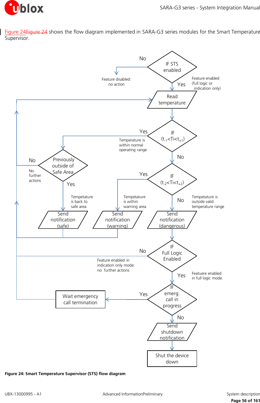
![SARA-G3 series - System Integration Manual UBX-13000995 - A1 Advanced InformationPreliminary System description Page 58 of 161 1.13.8.2 Threshold definitions When the module application operates at extreme temperatures with Smart Temperature Supervisor enabled, the user should note that outside the valid temperature range the device automatically shuts down as described above. The input for the algorithm is always the temperature measured within the wireless module (Ti, internal). This value can be higher than the working ambient temperature (Ta, ambient), since (for example) during transmission at maximum power a significant fraction of DC input power is dissipated as heat. This behavior is partially compensated by the definition of the upper shutdown threshold (t+2) that is slightly higher than the declared environmental temperature limit. Table 12Table 12 defines the temperature thresholds. Symbol Parameter Temperature Remarks t-2 Low temperature shutdown –40 °C Equal to the absolute minimum temperature rating for the wireless module (the lower limit of the extended temperature range) t-1 Low temperature warning –30 °C 10 °C above t-2 t+1 High temperature warning +85 °C 10 °C below t+2. The higher warning area for upper range ensures that any countermeasures used to limit the thermal heating will become effective, even considering some thermal inertia of the complete assembly. t+2 High temperature shutdown +95 °C Equal to the internal temperature Ti measured in the worst case operating condition at typical supply voltage when the ambient temperature Ta in the reference setup (*) equals the absolute maximum temperature rating (upper limit of the extended temperature range) (*) SARA-G3 series module mounted on a 79 mm x 62 mm x 1.41 mm 4-Layers PCB with a high coverage of copper in still air conditions Table 12: Thresholds definition for Smart Temperature Supervisor on the SARA-G3 series modules The sensor measures board temperature inside the shields, which can differ from ambient temperature. 1.13.9 AssistNow clients and GPS/GNSS integration Not supported by SARA-G300 and SARA-G310 modules. For customers using u-blox GPS/GNSS receivers, SARA-G350 modules feature embedded AssistNow clients. AssistNow A-GPS provides better GPS/GNSS performance and faster Time-To-First-Fix. The clients can be enabled and disabled with an AT command (see the u-blox AT Commands Manual [2]). SARA-G350 modules act as a stand-alone AssistNow client, making AssistNow available with no additional requirements for resources or software integration on an external host micro controller. Full access to u-blox positioning receivers is available via the SARA-G350 modules, through a dedicated DDC (I2C) interface, while the available GPIOs can handle the positioning chipset / module power-on/off. This means that the wireless module and the positioning chips and modules can be controlled through a single serial port from any host processor.](https://usermanual.wiki/u-blox/SARAG350.User-manual/User-Guide-2055502-Page-58.png)
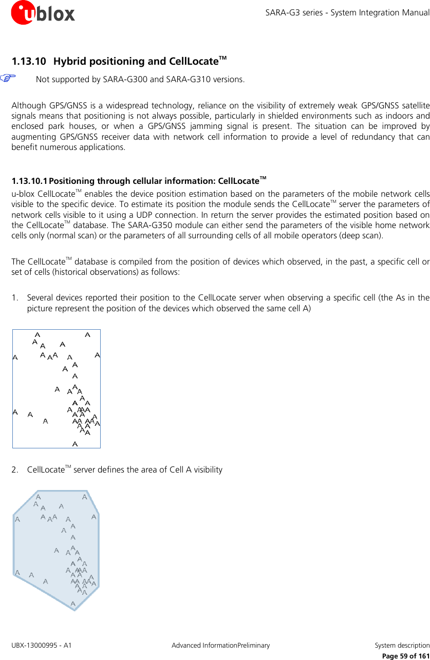
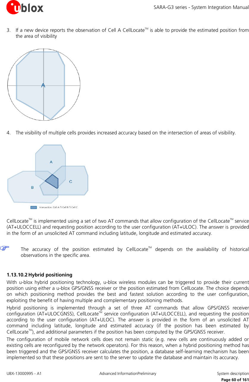
![SARA-G3 series - System Integration Manual UBX-13000995 - A1 Advanced InformationPreliminary System description Page 61 of 161 The use of hybrid positioning requires a connection via the DDC (I2C) bus between the SARA-G350 wireless module and the u-blox GPS/GNSS receiver (refer to section 2.5.3). Refer to GPS Implementation Application Note [21] for the complete description of the feature. u-blox is extremely mindful of user privacy. When a position is sent to the CellLocate server u-blox is unable to track the SIM used or the specific device. 1.13.11 Firmware upgrade Over AT (FOAT) 1.13.11.1 Overview This feature allows upgrading the module Firmware over the UART interface, using AT Commands. AT Command AT+UFWUPD triggers a reboot followed by the upgrade procedure at specified a baud rate (refer to u-blox AT Commands Manual [2] for more details) Both Xmodem-1k protocol (1024 bytes packets) and Xmodem protocol (128 bytes packets) can be used for downloading the new firmware image via a terminal application A special boot loader on the module performs firmware installation, security verifications and module reboot Firmware authenticity verification is performed via a security signature during the download. The firmware is then installed, overwriting the current version. In case of power loss during this phase, the boot loader detects a fault at the next wake-up, and restarts the firmware download from the Xmodem-1k handshake. After completing the upgrade, the module is reset again and wakes-up in normal boot 1.13.11.2 FOAT procedure The application processor must proceed in the following way: Send the AT+UFWUPD command through UART interface, specifying the file type and the desired baud rate Reconfigure serial communication at selected baud rate, without flow control with the used protocol Send the new FW image via the used protocol For more details, refer to the Firmware Update Application Note [22]. 1.13.12 Firmware upgrade Over The Air (FOTA) Not supported by SARA-G300 and SARA-G310 modules. Supported upon request on SARA-G350 modules. This feature allows upgrading the module Firmware over the air, i.e. over the GSM network. The main idea with updating Firmware over the air is to reduce the amount of data required for transmission to the module. This is achieved by downloading only a “delta file” instead of the full firmware. The delta contains only the differences between the two firmware versions (old and new), and is compressed. For more details, refer to the Firmware Update Application Note [22].](https://usermanual.wiki/u-blox/SARAG350.User-manual/User-Guide-2055502-Page-61.png)
![SARA-G3 series - System Integration Manual UBX-13000995 - A1 Advanced InformationPreliminary System description Page 62 of 161 1.13.13 In-Band modem (eCall / ERA-GLONASS) SARA-G350 module supports an In-Band modem solution for eCall and ERA-GLONASS emergency call applications over cellular networks, implemented according to 3GPP TS 26.267 [19], BS EN 16062:2011 [25] and ETSI TS 122 101 [26] specifications. eCall (European) and ERA-GLONASS (Russian) are initiatives to combine mobile communications and satellite positioning to provide rapid assistance to motorists in the event of a collision, implementing automated emergency response system based the first on GPS the latter on GLONASS positioning system. When activated, the in-vehicle systems (IVS) automatically initiate an emergency call carrying both voice and data (including location data) directly to the nearest Public Safety Answering Point (PSAP) to determine whether rescue services should be dispatched to the known position. Figure 25: eCall and ERA-GLONASS automated emergency response systems diagram flow 1.13.14 Power saving The power saving configuration is by default disabled, but it can be enabled using the AT+UPSV command. When power saving is enabled, the module automatically enters the low power idle-mode whenever possible, reducing current consumption. During low power idle-mode, the module is not ready to communicate with an external device by means of the application interfaces, since it is configured to reduce power consumption. It can be woken up from idle-mode to active-mode by the connected application processor, by the connected u-blox positioning receiver or by network activities, as described in Table 5Table 5. During idle-mode, the module processor core runs with the RTC 32 kHz reference clock, which is generated by: The internal 32 kHz oscillator, in case of SARA-G350 modules The 32 kHz signal provided at the EXT32K input pin, in case of SARA-G300 and SARA-G310 modules SARA-G300 and SARA-G310 need a 32 kHz signal at EXT32K input to reach the low power idle-mode. For the complete description of the AT+UPSV command, refer to the u-blox AT Commands Manual [2]. For the definition and the description of SARA-G3 series modules operating modes, including the events forcing transitions between the different operating modes, refer to section 1.4. For the description of current consumption in idle and active operating modes, refer to sections 1.5.1.2, 1.5.1.4. For the description of the UART settings related to module power saving configuration, refer to section 1.9.1.4. For the description of the EXT32K input and relativerelated application circuit design-in, refer to sections 1.6.4, 2.2.3.](https://usermanual.wiki/u-blox/SARAG350.User-manual/User-Guide-2055502-Page-62.png)
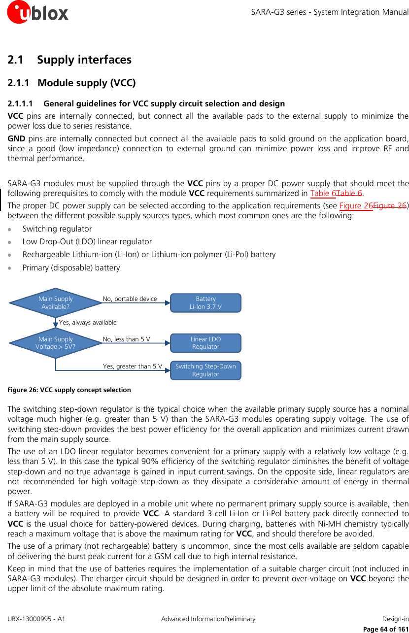
![SARA-G3 series - System Integration Manual UBX-13000995 - A1 Advanced InformationPreliminary Design-in Page 65 of 161 The usage of more than one DC supply at the same time should be carefully evaluated: depending on the supply source characteristics, different DC supply systems can result as mutually exclusive. The usage of a regulator or a battery not able to withstand the maximum peak current consumption specified in the SARA-G3 series Data Sheet [1] is generally not recommended. However, if the selected regulator or battery is not able to withstand the maximum peak current of the module, it must be able to withstand at least the maximum average current consumption value specified in the SARA-G3 series Data Sheet [1]. The additional energy required by the module during a GSM/GPRS Tx slot (when in the worst case the current consumption can rise up to 1.9 A, as described in section 1.5.1.2) can be provided by an appropriate bypass tank capacitor or supercapacitor with very large capacitance and very low ESR placed close to the module VCC pins. Depending on the actual capability of the selected regulator or battery, the required capacitance can be considerably larger than 1 mF and the required ESR can be in the range of few tens of mΩ. Carefully evaluate the implementation of this solution since aging and temperature conditions significantly affect the actual capacitor characteristics. The following sections highlight some design aspects for each of the supplies listed above providing application circuit design-in compliant with the module VCC requirements summarized in Table 6Table 6. For the additional specific guidelines for SARA-G350 ATEX modules integration in potentially explosive atmospheres applications, refer to section 2.13. 2.1.1.2 Guidelines for VCC supply circuit design using a switching regulator The use of a switching regulator is suggested when the difference from the available supply rail to the VCC value is high: switching regulators provide good efficiency transforming a 12 V or greater voltage supply to the typical 3.8 V value of the VCC supply. The characteristics of the switching regulator connected to VCC pins should meet the following prerequisites to comply with the module VCC requirements summarized in Table 6Table 6: Power capability: the switching regulator with its output circuit must be capable of providing a voltage value to the VCC pins within the specified operating range and must be capable of delivering 1.9 A current pulses with 1/8 duty cycle to the VCC pins Low output ripple: the switching regulator together with its output circuit must be capable of providing a clean (low noise) VCC voltage profile High switching frequency: for best performance and for smaller applications select a switching frequency ≥ 600 kHz (since L-C output filter is typically smaller for high switching frequency). The use of a switching regulator with a variable switching frequency or with a switching frequency lower than 600 kHz must be carefully evaluated since this can produce noise in the VCC voltage profile and therefore negatively impact GSM modulation spectrum performance. An additional L-C low-pass filter between the switching regulator output to VCC supply pins can mitigate the ripple on VCC, but adds extra voltage drop due to resistive losses on series inductors PWM mode operation: it is preferable to select regulators with Pulse Width Modulation (PWM) mode. While in connected-mode Pulse Frequency Modulation (PFM) mode and PFM/PWM mode, transitions must be avoided to reduce the noise on the VCC voltage profile. Switching regulators that are able to switch between low ripple PWM mode and high efficiency burst or PFM mode can be used, provided the mode transition occurs when the module changes status from idle/active-mode to connected-mode (where current consumption increases to a value greater than 100 mA): it is permissible to use a regulator that switches from the PWM mode to the burst or PFM mode at an appropriate current threshold (e.g. 60 mA) Output voltage slope: the use of the soft start function provided by some voltage regulators should be carefully evaluated, since the VCC pins voltage must ramp from 2.5 V to 3.2 V within 4 ms to switch on the module that otherwise can be switched on by a low level on PWR_ON pin](https://usermanual.wiki/u-blox/SARAG350.User-manual/User-Guide-2055502-Page-65.png)
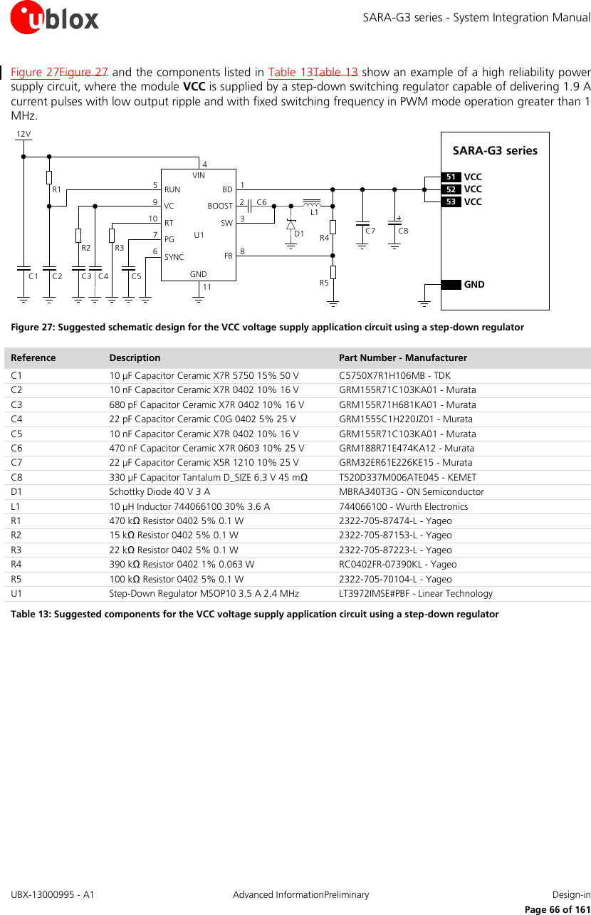
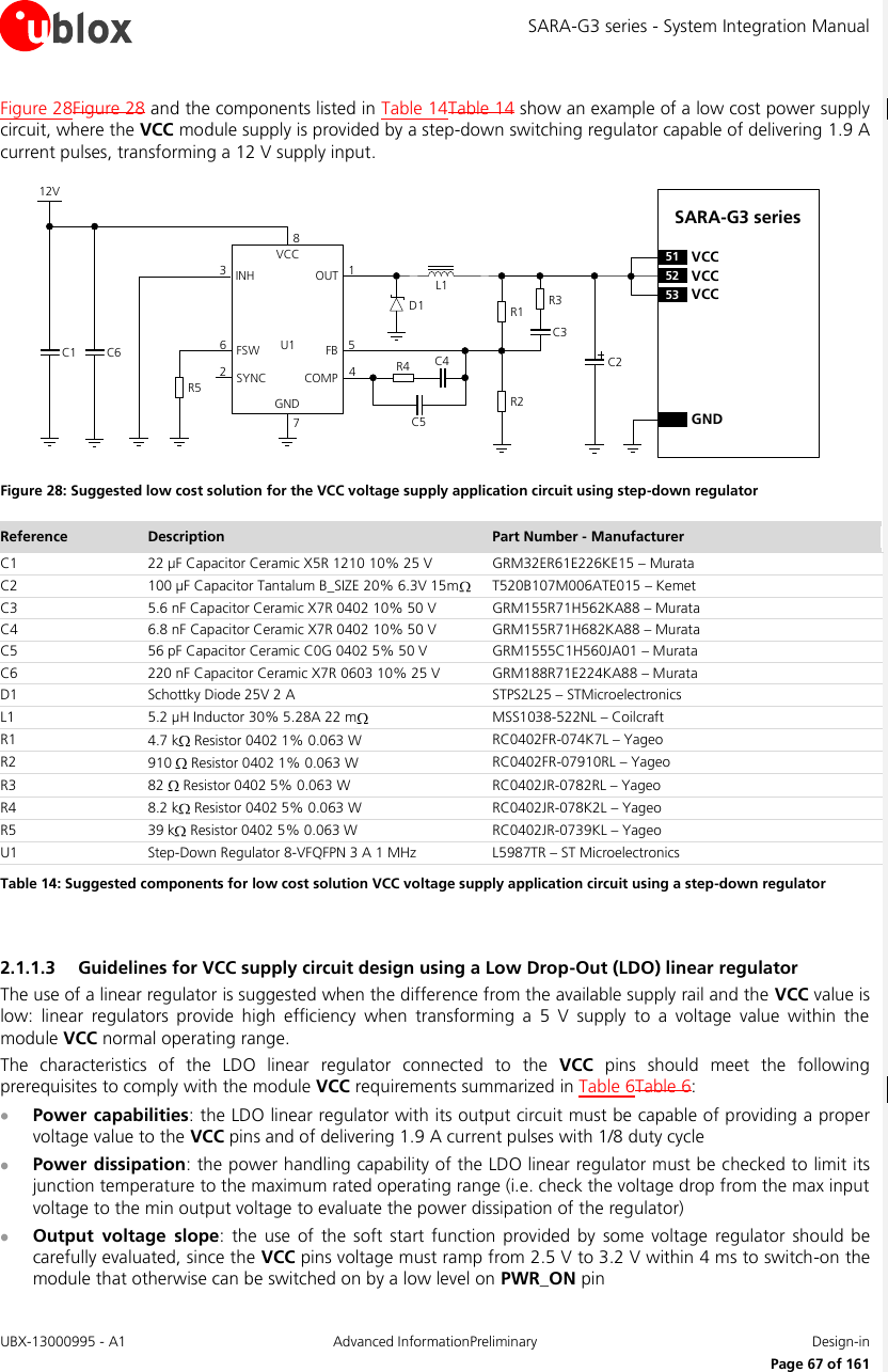
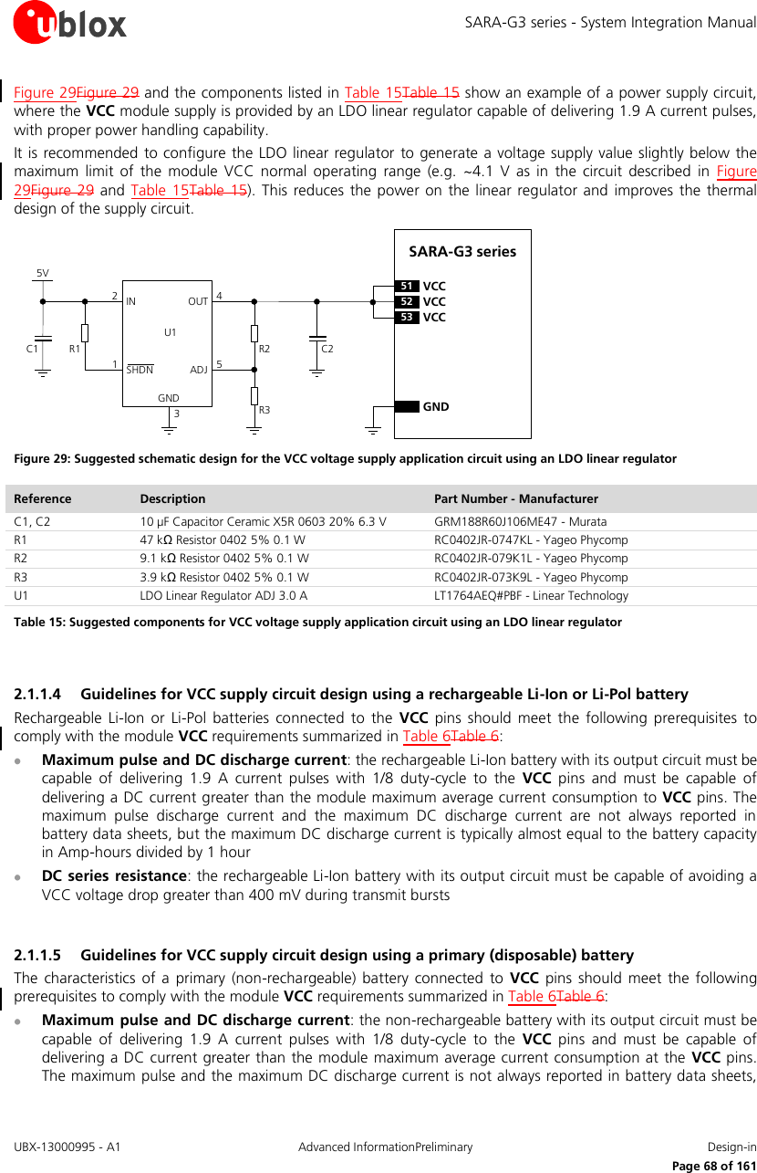
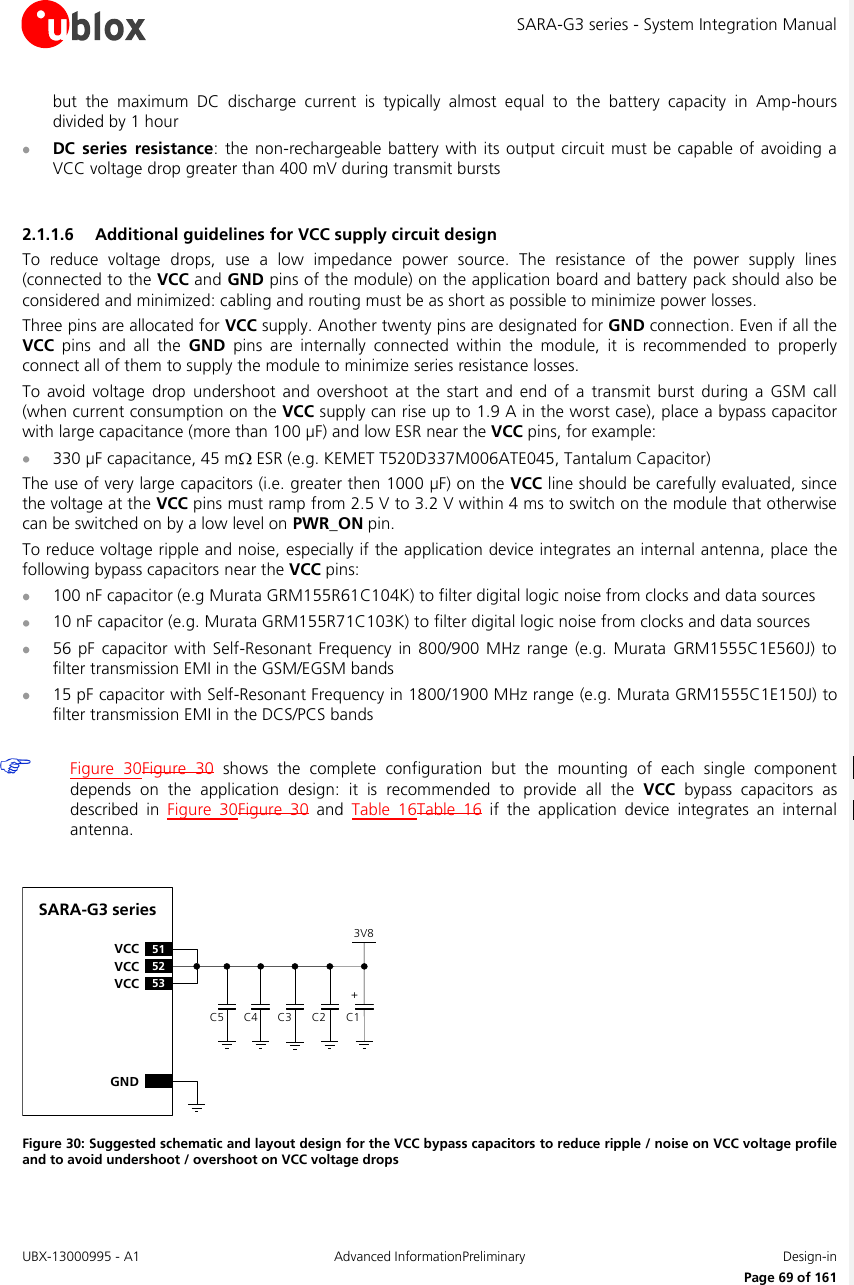
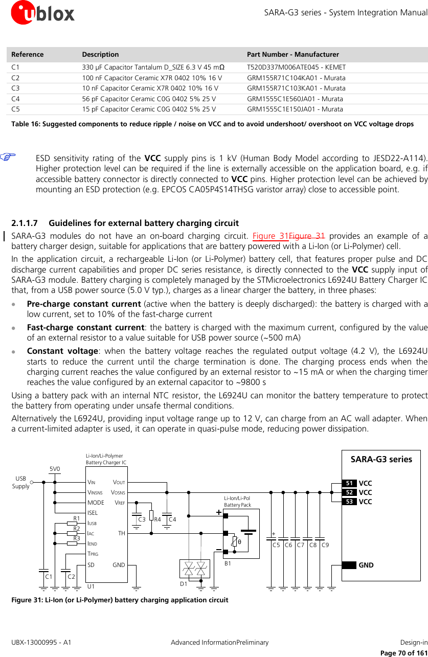
![SARA-G3 series - System Integration Manual UBX-13000995 - A1 Advanced InformationPreliminary Design-in Page 72 of 161 Connect each GND pin with application board solid GND layer. It is strongly recommended that each GND pad surrounding VCC pins have one or more dedicated via down to the application board solid ground layer. The VCC supply current flows back to main DC source through GND as ground current: provide adequate return path with suitable uninterrupted ground plane to main DC source. If the application board is a multilayer PCB, then it is required to connect together each GND area with complete via stack down to main board ground layer. It is recommended to implement one layer of the application board as ground plane as wide as possible. Good grounding of GND pads also ensures thermal heat sink. This is critical during call connection, when the real network commands the module to transmit at maximum power: proper grounding helps prevent module overheating. 2.1.2 RTC supply (V_BCKP) 2.1.2.1 Guidelines for V_BCKP circuit design If RTC timing is required to run for a time interval of T [s] at 25 °C when VCC supply is removed, place a capacitor with a nominal capacitance of C [µF] at the V_BCKP pin. Choose the capacitor using the following formula: C [µF] = (Current_Consumption [µA] x T [s]) / Voltage_Drop [V] = 1.5 x T [s] For example, a 100 µF capacitor (such as the Murata GRM43SR60J107M) can be placed at V_BCKP to provide a long buffering time. This capacitor holds V_BCKP voltage within its valid range for around 50 s at 25 °C, after the VCC supply is removed. If a very long buffering time is required, a 70 mF super-capacitor (e.g. Seiko Instruments XH414H-IV01E) can be placed at V_BCKP, with a 4.7 k series resistor to hold the V_BCKP voltage within its valid range for approximately 10 hours at 25 °C, after the VCC supply is removed. The purpose of the series resistor is to limit the capacitor charging current due to the large capacitor specifications, and also to let a fast rise time of the voltage value at the V_BCKP pin after VCC supply has been provided. These capacitors allow the time reference to run during battery disconnection. SARA-G3 seriesC1(a)2V_BCKPR2SARA-G3 seriesC2(superCap)(b)2V_BCKPD3SARA-G3 seriesB3(c)2V_BCKP Figure 32: Real time clock supply (V_BCKP) application circuits: (a) using a 100 µF capacitor to let the RTC run for ~50 s after VCC removal; (b) using a 70 mF capacitor to let RTC run for ~10 hours after VCC removal; (c) using a non-rechargeable battery Reference Description Part Number - Manufacturer C1 100 µF Tantalum Capacitor GRM43SR60J107M - Murata R2 4.7 kΩ Resistor 0402 5% 0.1 W RC0402JR-074K7L - Yageo Phycomp C2 70 mF Capacitor XH414H-IV01E - Seiko Instruments Table 18: Example of components for V_BCKP buffering](https://usermanual.wiki/u-blox/SARAG350.User-manual/User-Guide-2055502-Page-72.png)
![SARA-G3 series - System Integration Manual UBX-13000995 - A1 Advanced InformationPreliminary Design-in Page 73 of 161 If longer buffering time is required to allow the RTC time reference to run during a disconnection of the VCC supply, then an external battery can be connected to V_BCKP pin. The battery should be able to provide a proper nominal voltage and must never exceed the maximum operating voltage for V_BCKP (specified in the Input characteristics of Supply/Power pins table in SARA-G3 series Data Sheet [1]). The connection of the battery to V_BCKP should be done with a suitable series resistor for a rechargeable battery, or with an appropriate series diode for a non-rechargeable battery. The purpose of the series resistor is to limit the battery charging current due to the battery specifications, and also to allow a fast rise time of the voltage value at the V_BCKP pin after the VCC supply has been provided. The purpose of the series diode is to avoid a current flow from the module V_BCKP pin to the non-rechargeable battery. If the RTC timing is not required when the VCC supply is removed, it is not needed to connect the V_BCKP pin to an external capacitor or battery. In this case the date and time are not updated when VCC is disconnected. If VCC is always supplied, then the internal regulator is supplied from the main supply and there is no need for an external component on V_BCKP. Combining a SARA-G3 wireless module with a u-blox GPS/GNSS positioning receiver, the positioning receiver VCC supply is controlled by the wireless module by means of the “GPS supply enable” function provided by the GPIO2 of the wireless module. In this case the V_BCKP supply output of the SARA-G3 wireless module can be connected to the V_BCKP backup supply input pin of the GPS/GNSS receiver to provide the supply for the positioning real time clock and backup RAM when the VCC supply of the wireless module is within its operating range and the VCC supply of the GPS/GNSS receiver is disabled. This enables the u-blox GPS/GNSS receiver to recover from a power breakdown with either a hot start or a warm start (depending on the duration of the positioning VCC outage) and to maintain the configuration settings saved in the backup RAM. Refer to section 2.5.32.5.3 for more details regarding the application circuit with a u-blox GPS/GNSS receiver. On SARA-G300 and SARA-G310 modules, the V_BCKP supply output can be used to supply an external 32 kHz oscillator which provides a 32 kHz signal to the EXT32K input pin as reference clock for the RTC timing, so that the modules can enter the low power idle-mode and can make available the RTC functions. The internal regulator for V_BCKP is optimized for low leakage current and very light loads. Do not apply loads which might exceed the limit for maximum available current from V_BCKP supply, as this can cause malfunctions in the module. SARA-G3 series Data Sheet [1] describes the detailed electrical characteristics. V_BCKP supply output pin provides internal short circuit protection to limit start-up current and protect the device in short circuit situations. No additional external short circuit protection is required. ESD sensitivity rating of the V_BCKP supply pin is 1 kV (Human Body Model according to JESD22-A114). Higher protection level can be required if the line is externally accessible on the application board, e.g. if an accessible back-up battery connector is directly connected to V_BCKP pin. Higher protection level can be achieved by mounting an ESD protection (e.g. EPCOS CA05P4S14THSG varistor array) close to the accessible point. 2.1.2.2 Guidelines for V_BCKP layout design RTC supply (V_BCKP) requires careful layout: avoid injecting noise on this voltage domain as it may affect the stability of the 32 kHz oscillator.](https://usermanual.wiki/u-blox/SARAG350.User-manual/User-Guide-2055502-Page-73.png)
![SARA-G3 series - System Integration Manual UBX-13000995 - A1 Advanced InformationPreliminary Design-in Page 74 of 161 2.1.3 Interface supply (V_INT) 2.1.3.1 Guidelines for V_INT circuit design The V_INT digital interfaces 1.8 V supply output can be mainly used to: Pull-up DDC (I2C) interface signals (see section 2.5.3 for more details) Pull-up SIM detection signal (see section 2.42.4 for more details) Supply voltage translators to connect digital interfaces of the module to a 3.0 V device (see section 2.5.1) Supply a 1.8 V u-blox 6 or subsequent GPS/GNSS receiver (see section 2.5.3 for more details) Indicate when the module is switched on Do not apply loads which might exceed the limit for maximum available current from V_INT supply, as this can cause malfunctions in internal circuitry supplies to the same domain. SARA-G3 series Data Sheet [1] describes the detailed electrical characteristics. V_INT can only be used as an output; do not connect any external regulator on V_INT. Since the V_INT supply is generated by an internal switching step-down regulator, the V_INT voltage ripple can range from 15 mVpp during active-mode or connected-mode (when the switching regulator operates in PWM mode), to 90 mVpp in idle-mode (when the switching regulator operates in PFM mode). It is not recommended to supply sensitive analog circuitry without adequate filtering for digital noise. V_INT supply output pin provides internal short circuit protection to limit start-up current and protect the device in short circuit situations. No additional external short circuit protection is required. ESD sensitivity rating of the V_INT supply pin is 1 kV (Human Body Model according to JESD22-A114). Higher protection level could be required if the line is externally accessible on the application board. Higher protection level can be achieved by mounting an ESD protection (e.g. EPCOS CA05P4S14THSG varistor array) close to accessible point. If the V_INT supply output is not required by the customer application, since DDC (I2C) interface and SIM detection functions are not used and voltage translation of digital interfaces are not needed, the V_INT pin can be left unconnected to external components, but it is recommended providing direct access on the application board by means of accessible testpoint directly connected to the V_INT pin. 2.1.3.2 Guidelines for V_INT layout design V_INT digital interfaces supply output is generated by an integrated switching step-down converter, used internally to supply the digital interfaces. Because of this, it can be a source of noise: avoid coupling with sensitive signals. Formatted: English (U.S.)](https://usermanual.wiki/u-blox/SARAG350.User-manual/User-Guide-2055502-Page-74.png)
![SARA-G3 series - System Integration Manual UBX-13000995 - A1 Advanced InformationPreliminary Design-in Page 75 of 161 2.2 System functions interfaces 2.2.1 Module power-on (PWR_ON) 2.2.1.1 Guidelines for PWR_ON circuit design Connecting the PWR_ON input to a push button that shorts the PWR_ON pin to ground, provide an external pull-up resistor (e.g. 100 kΩ) biased by the V_BCKP supply pin of the module, as described in Figure 33Figure 33 and Table 19Table 19. Connecting the PWR_ON input to a push button, the pin will be externally accessible on the application device: according to EMC/ESD requirements of the application, provide an additional ESD protection (e.g. EPCOS CA05P4S14THSG varistor array) on the line connected to this pin, close to accessible point. The PWR_ON pin has high input impedance and is weakly pulled to the high level on the module. Avoid keeping it floating in a noisy environment. To hold the high logic level stable, the PWR_ON pin must be connected to a pull-up resistor (e.g. 100 kΩ) biased by the V_BCKP supply pin of the module. ESD sensitivity rating of the PWR_ON pin is 1 kV (Human Body Model according to JESD22-A114). Higher protection level can be required if the line is externally accessible on the application board, e.g. if an accessible push button is directly connected to PWR_ON pin. Higher protection level can be achieved by mounting an ESD protection (e.g. EPCOS CA05P4S14THSG varistor array) close to accessible point. When connecting the PWR_ON input to an external device (e.g. application processor), use an open drain output on the external device with an external pull-up resistor (e.g. 100 kΩ) biased by the V_BCKP supply pin of the module, as described in Figure 33Figure 33 and Table 19Table 19. A compatible push-pull output of an application processor can also be used: in this case the pull-up can be provided to pull the PWR_ON level high when the application processor is switched off. If the high-level voltage of the push-pull output pin of the application processor is greater than the maximum input voltage operating range of the V_BCKP pin (refer to SARA-G3 series Data Sheet [1]), the V_BCKP supply cannot be used to bias the pull-up resistor: the supply rail of the application processor or the module VCC supply could be used, but this increases the V_BCKP (RTC supply) current consumption when the module is in not-powered mode (VCC supply not present). Using a push-pull output of the external device, take care to fix the proper level in all the possible scenarios to avoid an inappropriate module switch-on. SARA-G3 seriesRext2V_BCKP15 PWR_ONPower-on push buttonESDOpen Drain OutputApplication ProcessorSARA-G3 seriesRext2V_BCKP15 PWR_ONTP TP Figure 33: PWR_ON application circuits using a push button and an open drain output of an application processor Reference Description Remarks Rext 100 kΩ Resistor 0402 5% 0.1 W External pull-up resistor ESD CT0402S14AHSG - EPCOS Varistor array for ESD protection Table 19: Example of pull-up resistor and ESD protection for the PWR_ON application circuit](https://usermanual.wiki/u-blox/SARAG350.User-manual/User-Guide-2055502-Page-75.png)
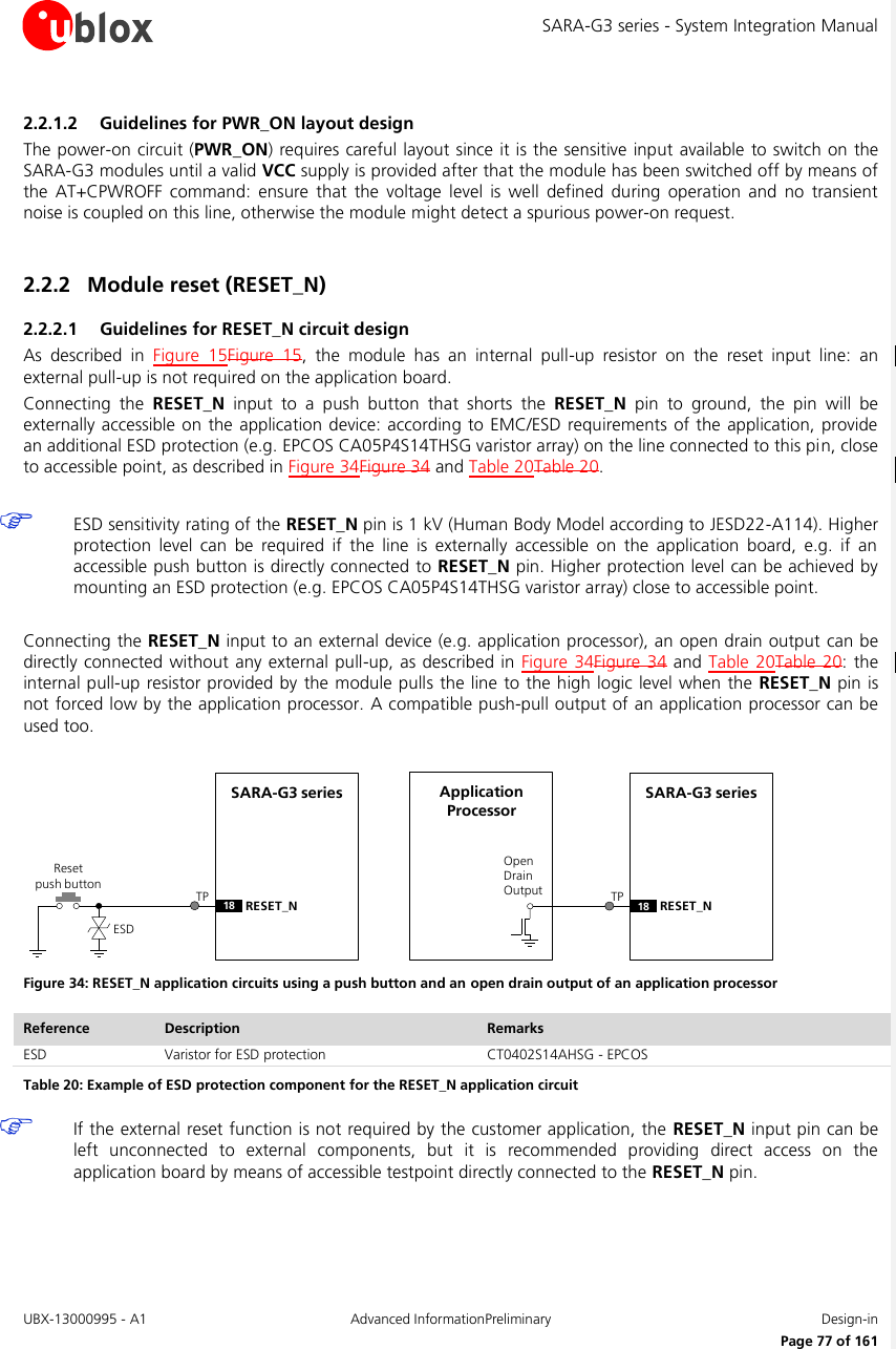
![SARA-G3 series - System Integration Manual UBX-13000995 - A1 Advanced InformationPreliminary Design-in Page 78 of 161 2.2.2.2 Guidelines for RESET_N layout design The reset circuit (RESET_N) requires careful layout due to the pin function: ensure that the voltage level is well defined during operation and no transient noise is coupled on this line, otherwise the module might detect a spurious reset request. It is recommended to keep the connection line to RESET_N as short as possible. 2.2.3 32 kHz signal (EXT32K and 32K_OUT) 2.2.3.1 Guidelines for EXT32K and 32K_OUT circuit design The application circuit of Figure 35Figure 35 describes how the 32K_OUT output pin of SARA-G300 / SARA-G310 modules can be connected to the EXT32K input pin, providing the 32 kHz signal which constitutes the Real Time Clock (RTC) reference clock, so that the modules can enter the low power idle-mode, reaching low current consumption figures (refer to the section 1.5.1.3 and to the SARA-G3 series Data Sheet [1]), and can provide the RTC functions when the module is switched on. 24 32K_OUTSARA-G300 SARA-G31031 EXT32K Figure 35: EXT32K application circuit using the 32 kHz signal provided by the 32K_OUT output The application circuit of Figure 36Figure 36 and Table 21Table 21 describe how an external oscillator can be connected to the EXT32K input pin of SARA-G300 / SARA-G310 modules, providing the external 32 kHz signal which constitutes the RTC reference clock, so that the modules can enter the very low power idle-mode, reaching very low current consumption figures (refer to the section 1.5.1.3 and to the SARA-G3 series Data Sheet [1]), and can provide the RTC functions when the RTC block is switched on since the V_BCKP voltage is within the valid range. 2V_BCKPGNDSARA-G300 SARA-G31031 EXT32K32 kHz OscillatorGNDCLKOUTOEVCCC1U1 Figure 36: EXT32K application circuit using an external 32 kHz oscillator Reference Description Remarks C1 100 nF Capacitor Ceramic X7R 0402 10% 16 V GRM155R61A104KA01 - Murata U1 Low Power Clock Oscillator 32.768 kHz OV-7604-C7 - Micro Crystal or SG-3040LC - EPSON TOYOCOM Table 21: Example of components for the EXT32K application circuit](https://usermanual.wiki/u-blox/SARAG350.User-manual/User-Guide-2055502-Page-78.png)
![SARA-G3 series - System Integration Manual UBX-13000995 - A1 Advanced InformationPreliminary Design-in Page 79 of 161 The two different solutions described in Figure 35Figure 35 and Figure 36Figure 36 are alternative and mutually exclusive: only one of the two proposed solutions must be implemented according to the required current consumption figures for the idle-mode (for the detailed characteristics refer to the SARA-G3 series Data Sheet [1]). As additional solution, alternative and mutually exclusive to the two described in Figure 35Figure 35 and Figure 36Figure 36, a proper 32 kHz signal can be provided to the EXT32K input by the used application processor, if capable. The EXT32K input and the 32K_OUT output are not available on SARA-G350 modules since the internal oscillator generates the 32 kHz RTC reference clock. ESD sensitivity rating of the EXT32K input pin and the 32K_OUT output pin is 1 kV (Human Body Model according to JESD22-A114). Higher protection level can be required if the line is externally accessible on the application board. Higher protection level can be achieved by mounting an ESD protection (e.g. EPCOS CA05P4S14THSG varistor array) close to accessible point. If the customer application does not require the low power idle-mode and the RTC functions, the EXT32K input pin and the 32K_OUT output pin can be left not connected. 2.2.3.2 Guidelines for EXT32K and 32K_OUT layout design The EXT32K input pin and the 32K_OUT output pin require accurate layout design: avoid injecting noise on these pins as it may affect the stability of the RTC timing reference.](https://usermanual.wiki/u-blox/SARAG350.User-manual/User-Guide-2055502-Page-79.png)
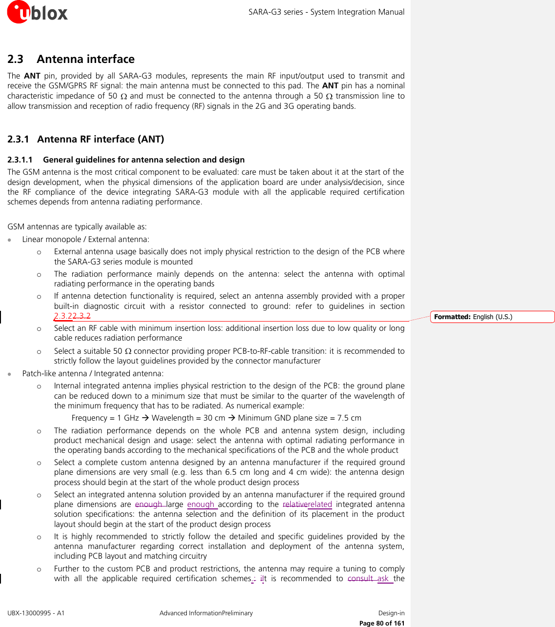
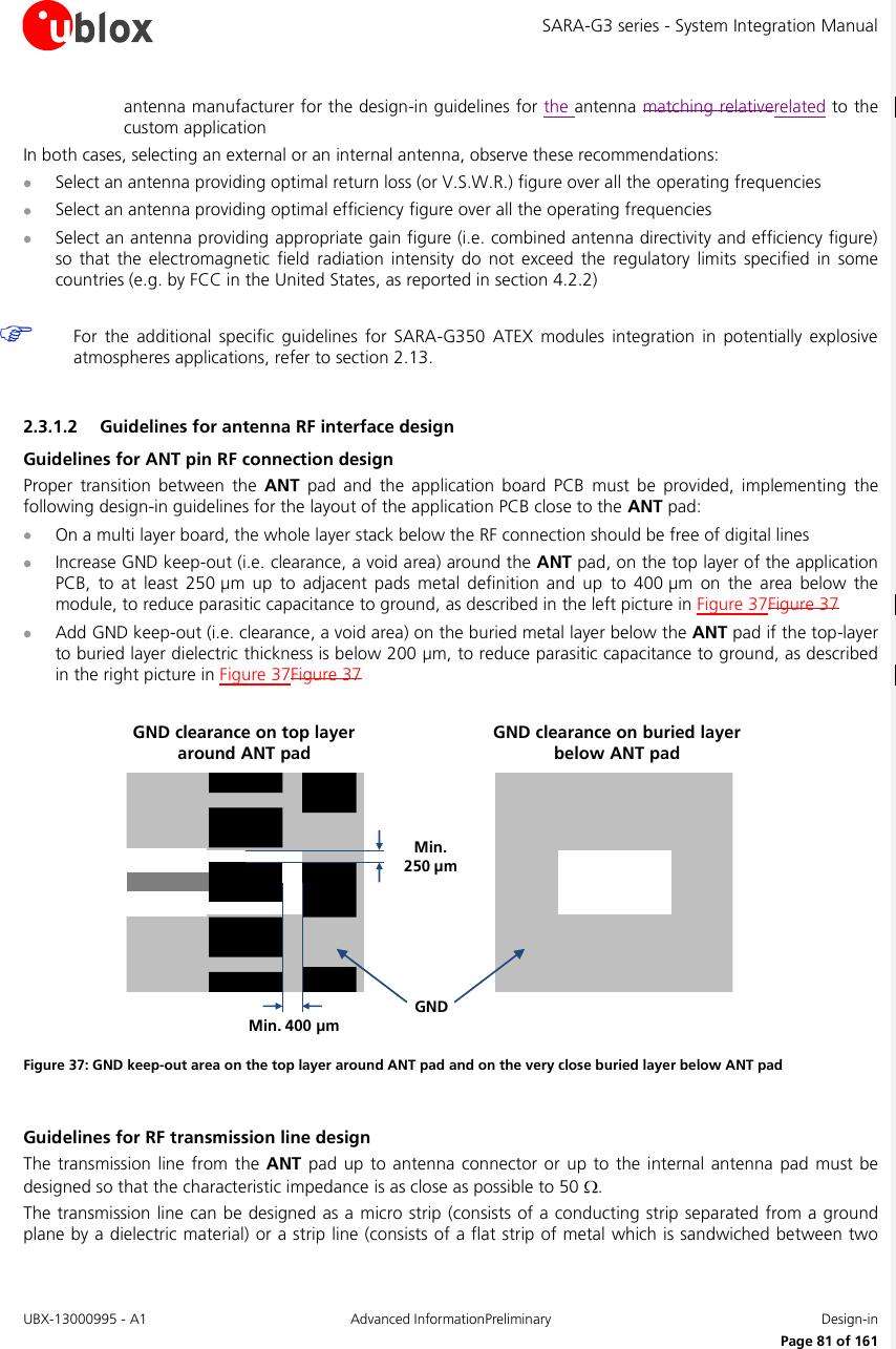
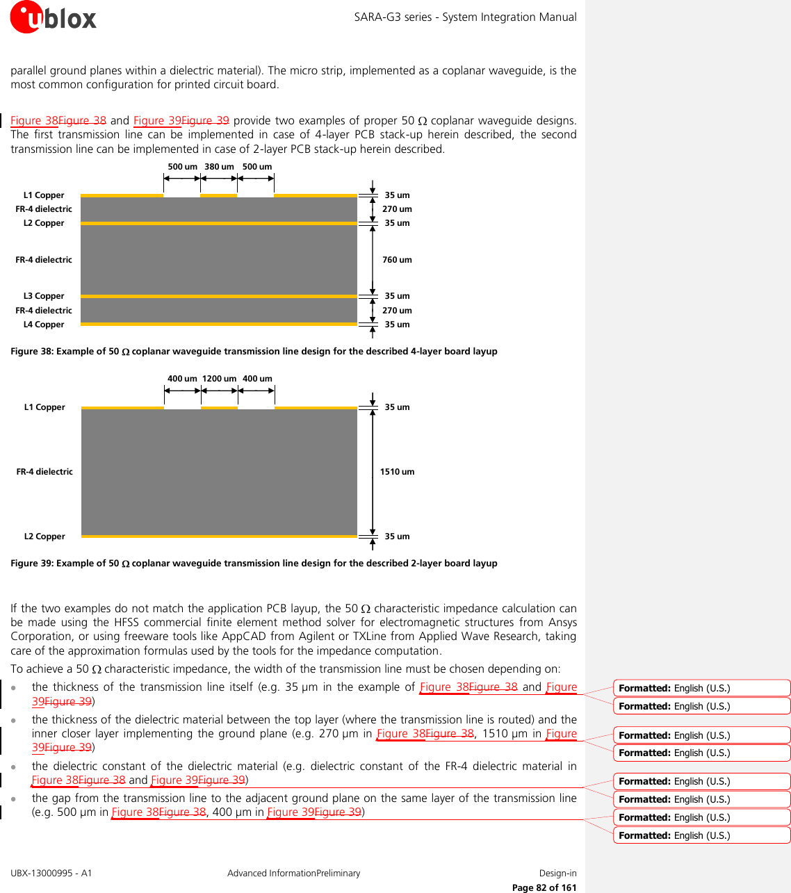
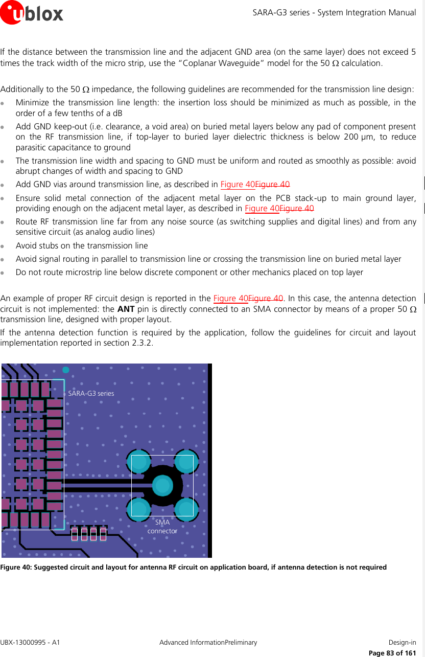
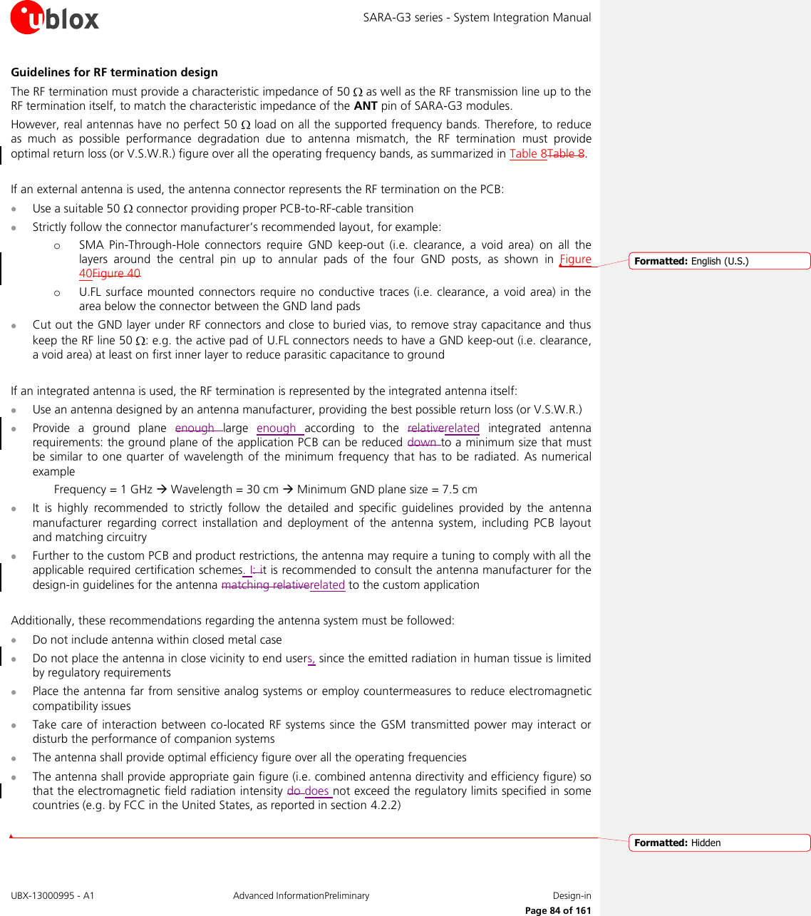
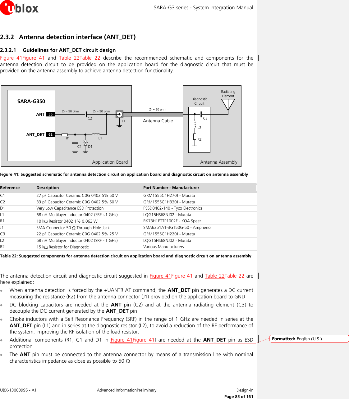
![SARA-G3 series - System Integration Manual UBX-13000995 - A1 Advanced InformationPreliminary Design-in Page 86 of 161 The DC impedance at RF port for some antennas may be a DC open (e.g. linear monopole) or a DC short to reference GND (e.g. PIFA antenna). For those antennas, without the diagnostic circuit of Figure 41Figure 41, the measured DC resistance is always at the limits of the measurement range (respectively open or short), and there is no mean to distinguish between a defect on antenna path with similar characteristics (respectively: removal of linear antenna or RF cable shorted to GND for PIFA antenna). Furthermore, any other DC signal injected to the RF connection from ANT connector to radiating element will alter the measurement and produce invalid results for antenna detection. It is recommended to use an antenna with a built-in diagnostic resistor in the range from 5 k to 30 k to assure good antenna detection functionality and avoid a reduction of module RF performance. The choke inductor should exhibit a parallel Self Resonance Frequency (SRF) in the range of 1 GHz to improve the RF isolation of load resistor. For example: Consider a GSM antenna with built-in DC load resistor of 15 k . Using the +UANTR AT command, the module reports the resistance value evaluated from the antenna connector provided on the application board to GND: Reported values close to the used diagnostic resistor nominal value (i.e. values from 13 k to 17 k if a 15 k diagnostic resistor is used) indicate that the antenna is properly connected Values close to the measurement range maximum limit (approximately 50 k ) or an open-circuit “over range” report (see u-blox AT Commands Manual [2]) means that that the antenna is not connected or the RF cable is broken Reported values below the measurement range minimum limit (1 k ) highlights a short to GND at antenna or along the RF cable Measurement inside the valid measurement range and outside the expected range may indicate an improper connection, damaged antenna or wrong value of antenna load resistor for diagnostic Reported value could differ from the real resistance value of the diagnostic resistor mounted inside the antenna assembly due to antenna cable length, antenna cable capacity and the used measurement method If the antenna detection function is not required by the customer application, the ANT_DET pin can be left not connected and the ANT pin can be directly connected to the antenna connector by means of a 50 transmission line as described in Figure 40Figure 40.](https://usermanual.wiki/u-blox/SARAG350.User-manual/User-Guide-2055502-Page-86.png)
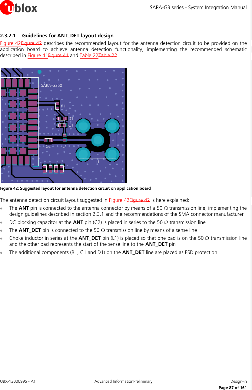
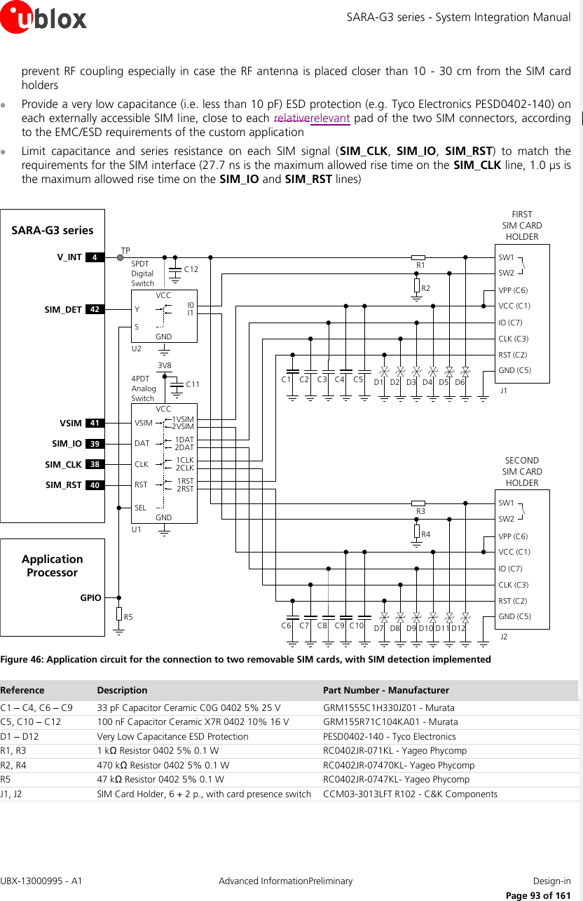
![SARA-G3 series - System Integration Manual UBX-13000995 - A1 Advanced InformationPreliminary Design-in Page 96 of 161 2.5 Serial interfaces 2.5.1 Asynchronous serial interface (UART) 2.5.1.1 Guidelines for UART circuit design Providing the full RS-232 functionality (using the complete V.24 link) If RS-232 compatible signal levels are needed, two different external voltage translators (e.g. Maxim MAX3237E and Texas Instruments SN74AVC8T245PW) can be used to provide full RS-232 (9 lines) functionality. The Texas Instruments chip provides the translation from 1.8 V to 3.3 V, while the Maxim chip provides the translation from 3.3 V to RS-232 compatible signal level. If a 1.8V application processor is used, for complete RS-232 functionality conforming to ITU Recommendation [9] in DTE/DCE serial communication, the complete UART interface of the module (DCE) must be connected to a 1.8 V application processor (DTE) as described in Figure 47Figure 47. TxDApplication Processor(1.8V DTE)RxDRTSCTSDTRDSRRIDCDGNDSARA-G3 series (1.8V DCE)12 TXD9DTR13 RXD10 RTS11 CTS6DSR7RI8DCDGND Figure 47: UART interface application circuit with complete V.24 link in DTE/DCE serial communication (1.8V DTE) If a 3.0 V Application Processor is used, appropriate unidirectional voltage translators must be provided using the module V_INT output as 1.8 V supply, as described in Figure 48Figure 48. 4V_INTTxDApplication Processor(3.0V DTE)RxDRTSCTSDTRDSRRIDCDGNDSARA-G3 series (1.8V DCE)12 TXD9DTR13 RXD10 RTS11 CTS6DSR7RI8DCDGND1V8B1 A1GNDU1B3A3VCCBVCCAUnidirectionalVoltage TranslatorC1 C23V0DIR3DIR2 OEDIR1VCCB2 A2B4A4DIR41V8B1 A1GNDU2B3A3VCCBVCCAUnidirectionalVoltage TranslatorC3 C43V0DIR1DIR3 OEB2 A2B4A4DIR4DIR2TP Figure 48: UART interface application circuit with complete V.24 link in DTE/DCE serial communication (3.0 V DTE) Reference Description Part Number - Manufacturer C1, C2, C3, C4 100 nF Capacitor Ceramic X7R 0402 10% 16 V GRM155R61A104KA01 - Murata U1, U2 Unidirectional Voltage Translator SN74AVC4T774 - Texas Instruments Table 27: Component for UART application circuit with complete V.24 link in DTE/DCE serial communication (3.0 V DTE)](https://usermanual.wiki/u-blox/SARAG350.User-manual/User-Guide-2055502-Page-96.png)
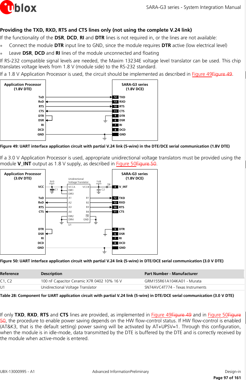
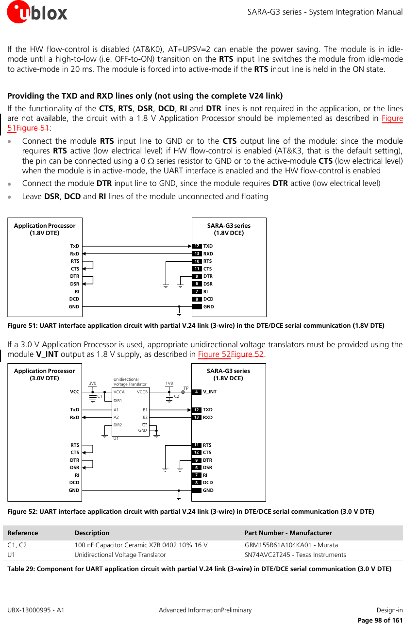
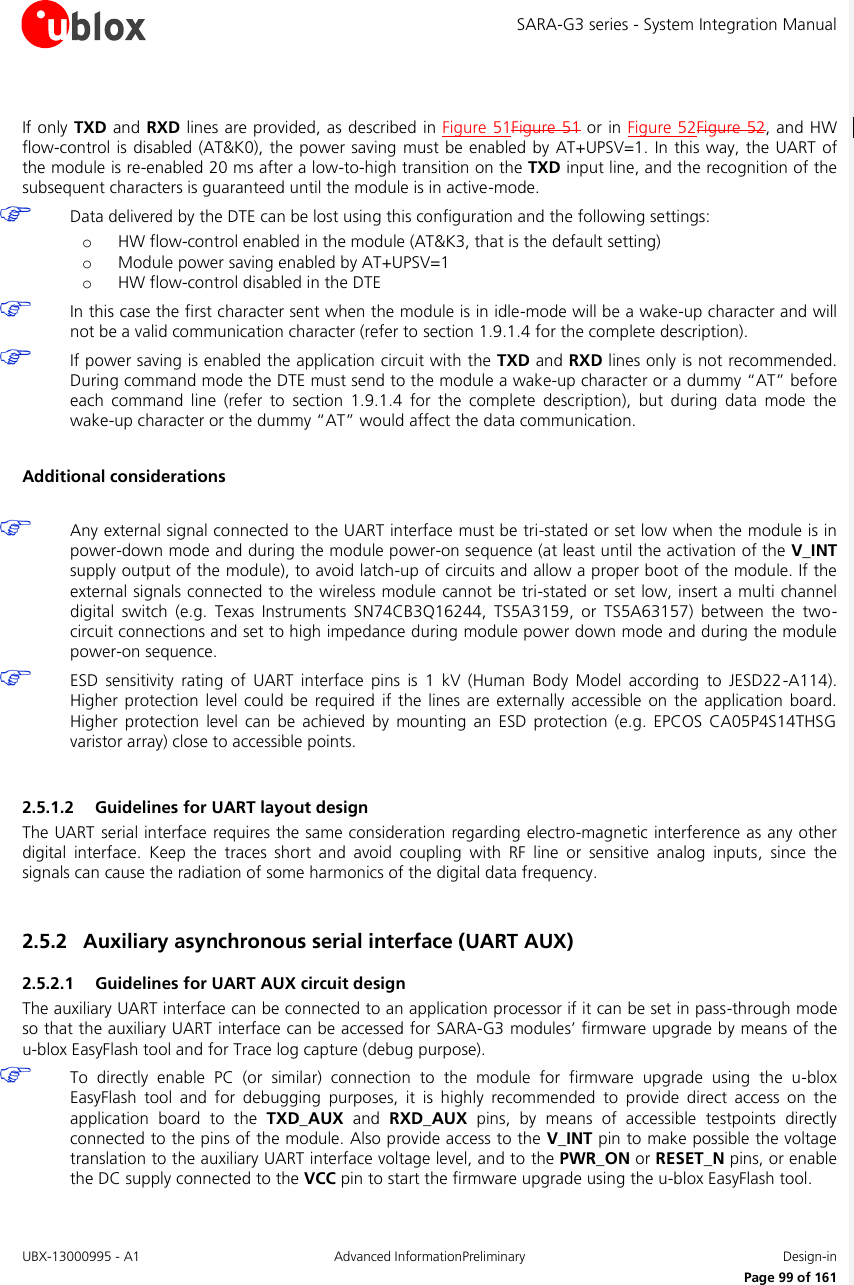
![SARA-G3 series - System Integration Manual UBX-13000995 - A1 Advanced InformationPreliminary Design-in Page 100 of 161 The circuit with a 1.8 V Application Processor should be implemented as described in Figure 51Figure 51. TxDApplication Processor(1.8V DTE)RxDSARA-G3 series (1.8V DCE)29 TXD_AUX28 RXD_AUXGND GND0 ohm0 ohmTestPointTestPoint Figure 53: UART AUX interface application circuit connecting a 1.8 V application processor If a 3.0 V Application Processor is used, appropriate unidirectional voltage translators must be provided using the module V_INT output as 1.8 V supply, as described in Figure 52Figure 52. 4V_INTTxDApplication Processor(3.0V DTE)RxDGNDSARA-G3 series (1.8V DCE)29 TXD_AUX28 RXD_AUXGND1V8B1 A1GNDU1VCCBVCCAUnidirectionalVoltage TranslatorC1 C23V0DIR1DIR2OEVCCB2 A20 ohm0 ohmTPTPTP Figure 54: UART AUX interface application circuit connecting a 3.0 V application processor Reference Description Part Number - Manufacturer C1, C2 100 nF Capacitor Ceramic X7R 0402 10% 16 V GRM155R61A104KA01 - Murata U1 Unidirectional Voltage Translator SN74AVC2T245 - Texas Instruments Table 30: Component for UART AUX interface application circuit connecting a 3.0 V application processor Refer to Firmware Update Application Note [22] for additional guidelines regarding the procedure for SARA-G3 modules’ firmware upgrade over the auxiliary UART interface using the u-blox EasyFlash tool. Any external signal connected to the auxiliary UART interface must be tri-stated or set low when the module is in power-down mode and during the module power-on sequence (at least until the activation of the V_INT supply output of the module), to avoid latch-up of circuits and allow a proper boot of the module. If the external signals connected to the wireless module cannot be tri-stated or set low, insert a multi channel digital switch (e.g. Texas Instruments SN74CB3Q16244, TS5A3159, or TS5A63157) between the two-circuit connections and set to high impedance during module power down mode and during the module power-on sequence. ESD sensitivity rating of auxiliary UART pins is 1 kV (Human Body Model according to JESD22-A114). Higher protection level could be required if the lines are externally accessible on the application board. Higher protection level can be achieved by mounting an ESD protection (e.g. EPCOS CA05P4S14THSG varistor array) close to accessible points. 2.5.2.2 Guidelines for UART AUX layout design The auxiliary UART serial interface is not critical for the layout design since it is not used during normal operation of SARA-G3 modules. Ensure accessibility to the TXD_AUX and RXD_AUX pins providing test points on the application board.](https://usermanual.wiki/u-blox/SARAG350.User-manual/User-Guide-2055502-Page-100.png)
![SARA-G3 series - System Integration Manual UBX-13000995 - A1 Advanced InformationPreliminary Design-in Page 101 of 161 2.5.3 DDC (I2C) interface 2.5.3.1 Guidelines for DDC (I2C) circuit design The SDA and SCL lines must be connected to the DDC (I2C) interface pins of the u-blox GPS/GNSS receiver (i.e. the SDA2 and SCL2 pins of the u-blox positioning receiver) on the application board to allow the communication between the wireless module and the u-blox GPS/GNSS receiver, enabled by the AT+UGPS command (for more details refer to u-blox AT Commands Manual [2]). To be compliant to the I2C bus specifications, the module bus interface pads are open drain output and pull up resistors must be used conforming to the I2C bus specifications [13]. Since the pull-up resistors are not mounted on the module, they must be mounted externally. Provide external pull-ups resistors (e.g. 4.7 k ) on SDA and SCL lines and connect them to the V_INT 1.8 V supply source, or another 1.8 V supply source enabled after V_INT (e.g., as the 1.8 V supply present in the application circuit of Figure 55Figure 55, controlled by the wireless module). The signal shape is defined by the values of the pull-up resistors and the bus capacitance. Long wires on the bus increase the capacitance. If the bus capacitance is increased, use pull-up resistors with nominal resistance value lower than 4.7 k , to match the I2C bus specifications [13] regarding rise and fall times of the signals. Capacitance and series resistance must be limited on the bus to match the I2C specifications (1.0 µs is the maximum allowed rise time on the SCL and SDA lines): route connections as short as possible. If the pins are not used as DDC bus interface, they can be left unconnected. The following special features over GPIOs can be optionally implemented on the application board to improve the integration of SARA-G350 wireless modules with a u blox GPS/GNSS receiver: The GPIO2, by default configured to provide the “GPS supply enable” function, must be connected to the active-high enable pin (or the active-low shutdown pin) of the voltage regulator that supplies the u-blox positioning receiver on the application board to enable or disable the supply of the u-blox GPS/GNSS receiver connected to the wireless module by the AT+UGPS command The GPIO3, by default configured to provide the “GPS data ready” function, must be connected to the data ready output of the u-blox positioning receiver (i.e. the pin TXD1 of the u-blox GPS/GNSS receiver) on the application board, to sense when the u-blox positioning receiver connected to the wireless module is ready to send data by the DDC (I2C) interface The GPIO4, by default configured to provide the “GPS RTC sharing” function, must be connected to the RTC synchronization signal of the u-blox positioning receiver (i.e. the pin EXTINT0 of the u-blox GPS/GNSS receiver) on the application board, to provide an RTC (Real Time Clock) synchronization signal at the power up of the u-blox positioning receiver connected to the wireless module “GPS data ready” and “GPS RTC sharing” functions are not supported by all u-blox GPS/GNSS receivers HW or ROM/FW versions. Refer to the GPS Implementation Application Note [21] or to the Hardware Integration Manual of the u-blox GPS/GNSS receivers for the supported features. Figure 55Figure 55 illustrates an application circuit for SARA-G350 connection to a u-blox 1.8 V GPS/GNSS receiver: The SDA and SCL pins of the SARA-G350 module are directly connected to the relativerelated pins of the u-blox 1.8 V GPS/GNSS receiver, with appropriate pull-up resistors. The GPIO3 and GPIO4 pins are directly connected respectively to TXD1 and EXTINT0 pins of the u-blox 1.8 V GPS/GNSS receiver providing “GPS data ready” and “GPS RTC sharing” functions.](https://usermanual.wiki/u-blox/SARAG350.User-manual/User-Guide-2055502-Page-101.png)
![SARA-G3 series - System Integration Manual UBX-13000995 - A1 Advanced InformationPreliminary Design-in Page 102 of 161 The GPIO2 pin is connected to the active-high enable pin of the voltage regulator that supplies the u-blox 1.8 V GPS/GNSS receiver providing the “GPS supply enable” function. A pull-down resistor is provided to avoid a switch on of the positioning receiver when the SARA-G350 module is switched off or in the reset state. The V_BCKP supply output of the SARA-G350 wireless module is connected to the V_BCKP backup supply input pin of the GPS/GNSS receiver to provide the supply for the GPS/GNSS real time clock and backup RAM when the VCC supply of the wireless module is within its operating range and the VCC supply of the GPS/GNSS receiver is disabled. This enables the u-blox GPS/GNSS receiver to recover from a power breakdown with either a Hot-start or a Warm-start (depending on the actual duration of the GPS/GNSS VCC outage) and to maintain the configuration settings saved in the backup RAM. SARA-G350R1INOUTGNDGPS LDORegulatorSHDNu-blox GPS/GNSS1.8 V receiverSDA2SCL2R21V8 1V8VMAIN1V8U123 GPIO2SDASCLC1TxD1EXTINT0GPIO3GPIO426272425VCCR3V_BCKP V_BCKP2 Figure 55: DDC (I2C) application circuit for u-blox 1.8 V GPS/GNSS receiver Reference Description Part Number - Manufacturer R1, R2 4.7 kΩ Resistor 0402 5% 0.1 W RC0402JR-074K7L - Yageo Phycomp R3 47 kΩ Resistor 0402 5% 0.1 W RC0402JR-0747KL - Yageo Phycomp U1 Voltage Regulator for GPS/GNSS Receiver See GPS/GNSS Receiver Hardware Integration Manual Table 31: Components for DDC (I2C) application circuit for u-blox 1.8 V GPS/GNSS receiver As an alternative to using an external voltage regulator, the V_INT supply output of SARA-G350 wireless modules can be used to supply a u-blox 1.8 V GPS/GNSS receiver of the u-blox 6 family (or later u-blox family). The V_INT supply is able to withstand the maximum current consumption of these positioning receivers. The V_INT supply output provides low voltage ripple (up to 15 mVpp) when the module is in active-mode or in connected-mode, but it provides higher voltage ripple (up to 90 mVpp) when the module is in the low power idle-mode with power saving configuration enabled by AT+UPSV (refer to u-blox AT Commands Manual [2]). According to the voltage ripple characteristic of the V_INT supply output: The power saving configuration cannot be enabled to properly supply by V_INT output any 1.8 V GPS/GNSS receiver of the u-blox 6 family and any 1.8 V GPS/GNSS receiver of the u-blox 7 family with TCXO The power saving configuration can be enabled to properly supply by V_INT output any 1.8 V GPS/GNSS receiver of the u-blox 7 family without TCXO Additional filtering may be needed to properly supply an external LNA, depending on the characteristics of the used LNA, adding a series ferrite bead and a bypass capacitor (e.g. the Murata BLM15HD182SN1 ferrite bead and the Murata GRM1555C1H220J 22 pF capacitor) at the input of the external LNA supply line. Refer to the GPS Implementation Application Note [21] for additional guidelines using the V_INT supply output of SARA-G350 wireless modules to supply a u-blox 1.8 V GPS/GNSS receiver.](https://usermanual.wiki/u-blox/SARAG350.User-manual/User-Guide-2055502-Page-102.png)
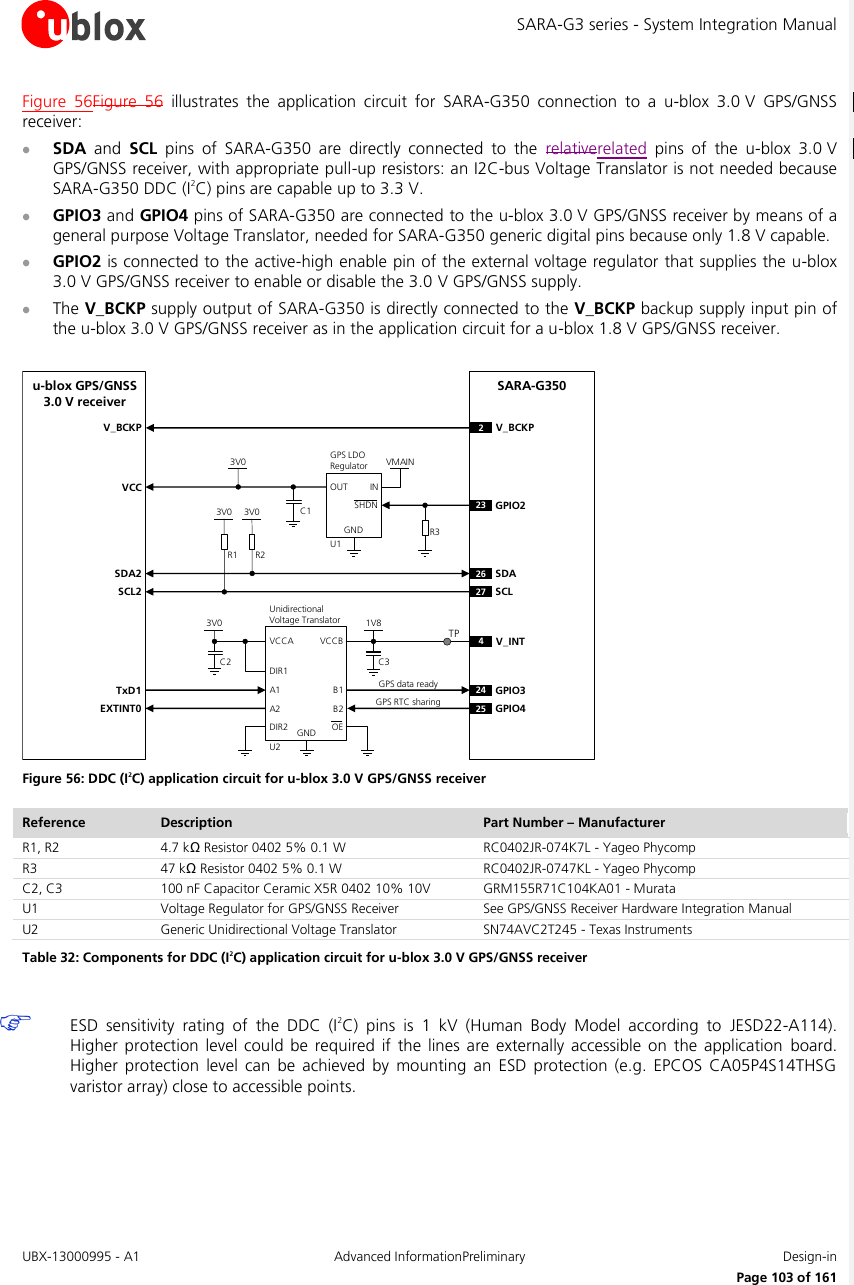
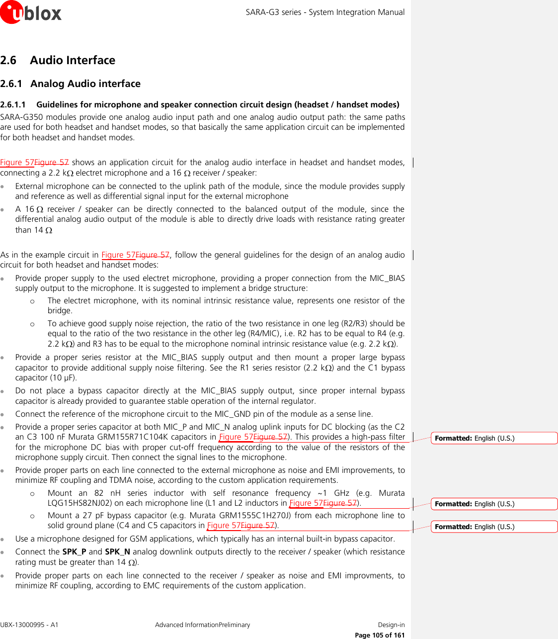
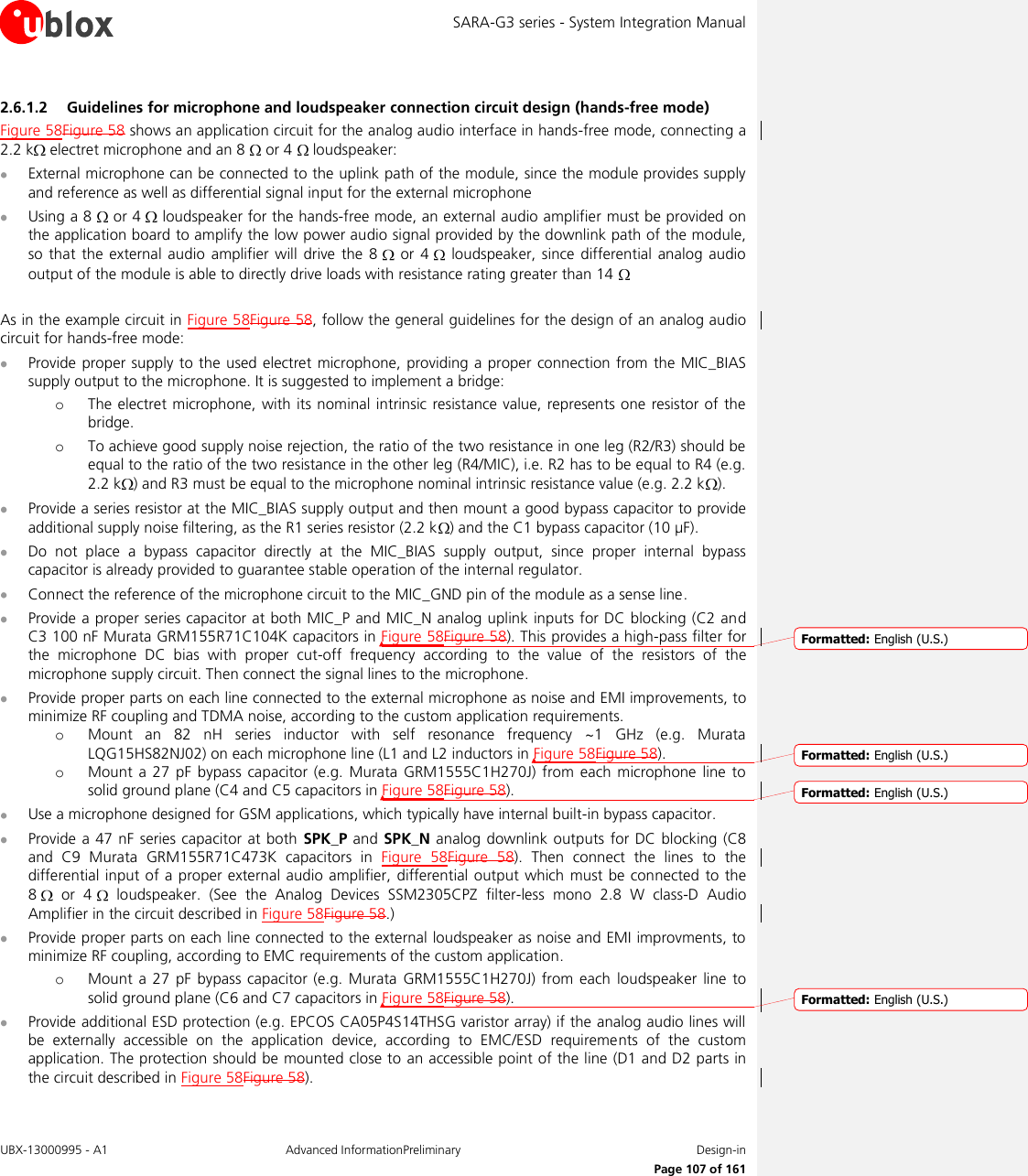
![SARA-G3 series - System Integration Manual UBX-13000995 - A1 Advanced InformationPreliminary Design-in Page 109 of 161 2.6.1.3 Guidelines for external analog audio device connection circuit design The differential analog audio input / output can be used to connect the module to an external analog audio device. Audio devices with a differential analog input / output are preferable, as they are more immune to external disturbances. Figure 59Figure 59 and Table 35Table 35 describe the application circuits, following the suggested circuit design-in. Guidelines for the connection to a differential analog audio input: The SPK_P / SPK_N balanced output of the module must be connected to the differential input of the external audio device by means of series capacitors for DC blocking (e.g. 10 µF Murata GRM188R60J106M) to decouple the bias present at the module output, as described in the left side of Figure 59Figure 59 Guidelines for the connection to a single ended analog audio input: A proper differential to single ended circuit must be inserted from the SPK_P / SPK_N balanced output of the module to the single ended input of the external audio device, as described in the right side of Figure 59Figure 59: 10 µF series capacitors (e.g. Murata GRM188R60J106M) are provided to decouple the bias present at the module output, and a voltage divider is provided to properly adapt the signal level from the module output to the external audio device input Guidelines for the connection to a differential analog audio output: The MIC_P / MIC_N balanced input of the module must be connected to the differential output of the external audio device by means of series capacitors for DC blocking (e.g. 10 µF Murata GRM188R60J106M) to decouple the bias present at the module input, as described in the left side of Figure 59Figure 59 Guidelines for the connection to a single ended analog audio output: A proper single ended to differential circuit has to be inserted from the single ended output of the external audio device to the MIC_P / MIC_N balanced input of the module, as described in the right side of Figure 59Figure 59: 10 µF series capacitors (e.g. Murata GRM188R60J106M) are provided to decouple the bias present at the module input, and a voltage divider is provided to properly adapt the signal level from the external audio device output to the module input Additional guidelines for any connection: The DC-block series capacitor acts as high-pass filter for audio signals, with cut-off frequency depending on both the values of capacitor and on the input impedance of the device. For example: in case of differential input impedance of 600 , the two 10 µF capacitors will set the -3 dB cut-off frequency to 53 Hz, while for single ended connection to 600 external device, the cut-off frequency with just the single 10 µF capacitor will be 103 Hz. In both cases the high-pass filter has a low enough cut-off to not impact the audio signal frequency response Use a suitable power-on sequence to avoid audio bump due to charging of the capacitor: the final audio stage should be always enabled as last one The signal levels can be adapted by setting gain using AT commands (refer to the u-blox AT Commands Manual [2][2], +USGC, +UMGC), but additional circuitry must be inserted if the SPK_P / SPK_N output level of the module is too high for the input of the audio device or if the output level of the audio device is too high for MIC_P / MIC_N, as the voltage dividers present in the circuits described in the right side of Figure 59Figure 59 to properly adapt the signal level Formatted: English (U.S.)Formatted: English (U.S.)Formatted: English (U.S.)Formatted: English (U.S.)Formatted: English (U.S.)Formatted: English (U.S.), Do notcheck spelling or grammar](https://usermanual.wiki/u-blox/SARAG350.User-manual/User-Guide-2055502-Page-109.png)
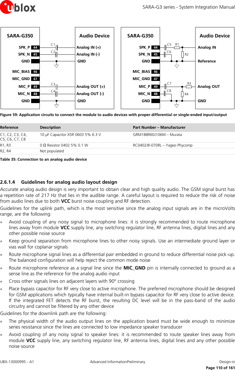
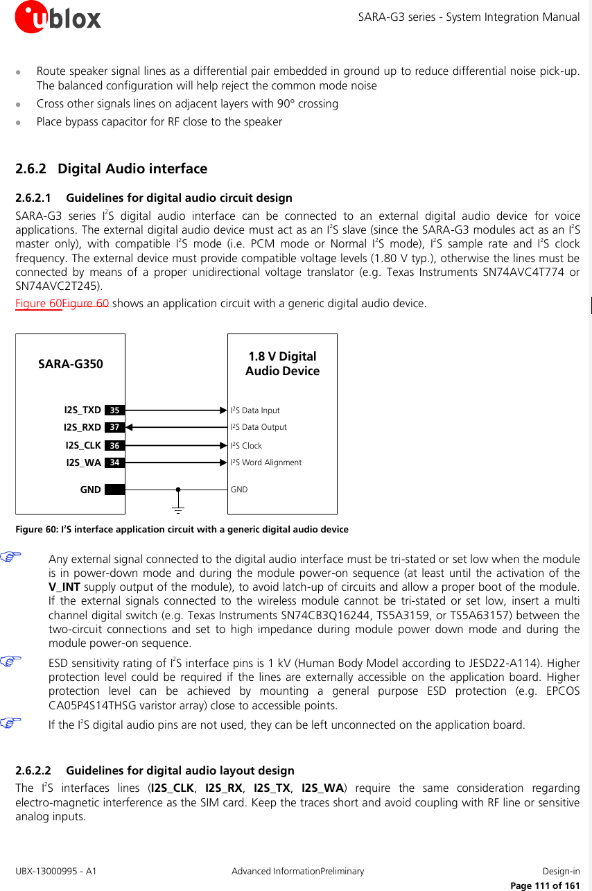
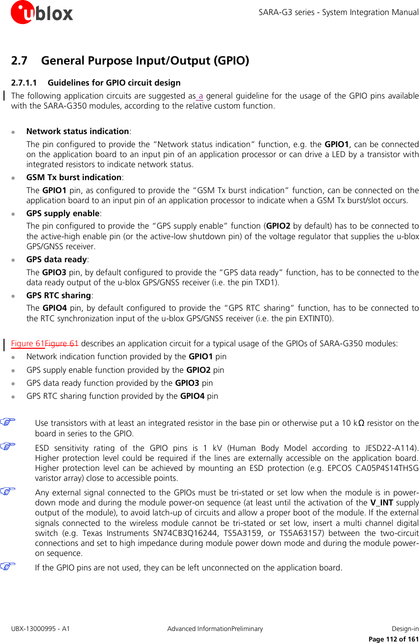
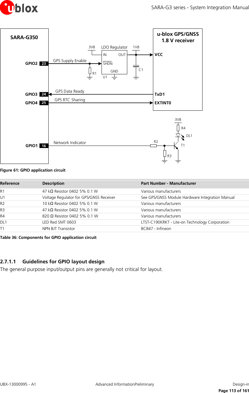
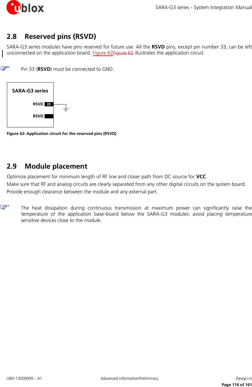
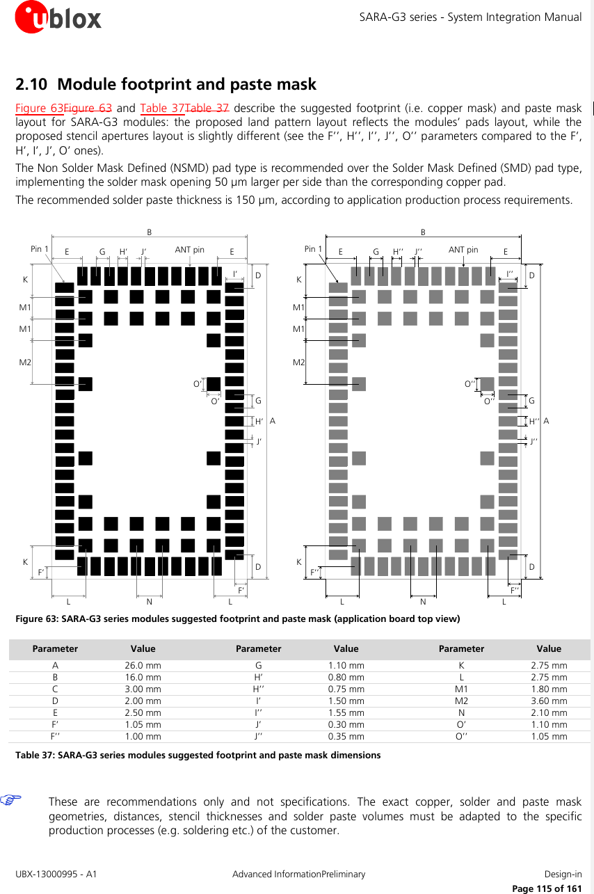
![SARA-G3 series - System Integration Manual UBX-13000995 - A1 Advanced InformationPreliminary Design-in Page 117 of 161 2.11 Thermal guidelines SARA-G3 series module operating temperature range and module thermal resistance are specified in the SARA-G3 series Data Sheet [1]. The most critical condition concerning module thermal performance is the uplink transmission at maximum power (data upload or voice call in connected-mode), when the baseband processor runs at full speed, radio circuits are all active and the RF power amplifier is driven to higher output RF power. This scenario is not often encountered in real networks; however the application should be correctly designed to cope with it. During transmission at maximum RF power the SARA-G3 series modules generate thermal power that can exceed 1 W: this is an indicative value since the exact generated power strictly depends on operating condition such as the number of allocated TX slot, transmitting frequency band, etc. The generated thermal power must be adequately dissipated through the thermal and mechanical design of the application. The spreading of the Module-to-Ambient thermal resistance (Rth,M-A) depends on the module operating condition (e.g. GSM or GPRS mode, transmit band): the overall temperature distribution is influenced by the configuration of the active components during the specific mode of operation and their different thermal resistance toward the case interface. Mounting a SARA-G3 series module on a 79 mm x 62 mm x 1.41 mm 4-Layers PCB with a high coverage of copper in still air conditions8, the increase of the module temperature9 in different modes of operation, referred to idle state initial condition10, can be summarized as following: ~8 °C during a GSM voice call (1 TX slot, 1 RX slot) at max TX power ~12 °C during a GPRS data transfer (2 TX slots, 3 RX slots) at max TX power The Module-to-Ambient thermal resistance value and the relative increase of module temperature will be different for other mechanical deployments of the module, e.g. PCB with different dimensions and characteristics, mechanical shells enclosure, or forced air flow. The increase of thermal dissipation, i.e. the Module-to-Ambient thermal resistance reduction, will decrease the temperature for internal circuitry of SARA-G3 series modules for a given operating ambient temperature. This improves the device long-term reliability for applications operating at high ambient temperature. A few hardware techniques may be used to reduce the Module-to-Ambient thermal resistance in the application: Connect each GND pin with solid ground layer of the application board and connect each ground area of the multilayer application board with complete via stack down to main ground layer Provide a ground plane as wide as possible on the application board Optimize antenna return loss, to optimize overall electrical performance of the module including a decrease of module thermal power Optimize the thermal design of any high-power component included in the application, as linear regulators and amplifiers, to optimize overall temperature distribution in the application device Select the material, the thickness and the surface of the box (i.e. the mechanical enclosure of the application device that integrates the module) so that it provides good thermal dissipation Force ventilation air-flow within mechanical enclosure 8 Refer to SARA-G3 series Data Sheet [1] for the Rth,M-A value in this application condition 9 Temperature is measured by internal sensor of wireless module 10 Steady state thermal equilibrium is assumed. The module’s temperature in idle state can be considered equal to ambient temperature](https://usermanual.wiki/u-blox/SARAG350.User-manual/User-Guide-2055502-Page-117.png)
![SARA-G3 series - System Integration Manual UBX-13000995 - A1 Advanced InformationPreliminary Design-in Page 118 of 161 Provide a heat sink component attached to the module top side, with electrically insulated / high thermal conductivity adhesive, or on the backside of the application board, below the wireless module For example, after the installation of a robust aluminum heat-sink with forced air ventilation on the back of the same application board described above, the Module-to-Ambient thermal resistance (Rth,M-A) is reduced up to the Module-to-Case thermal resistance (Rth,M-C) defined in the SARA-G3 series Data Sheet [1]. The effect of lower Rth,M-A can be seen from the module temperature increase, which now can be summarized as following: ~1 °C during a GSM voice call (1 TX slot, 1 RX slot) at the maximum TX power ~2 °C during a GPRS data transfer (2 TX slots, 3 RX slots) at the maximum TX power Beside the reduction of the Module-to-Ambient thermal resistance implemented by the hardware design of the application device integrating a SARA-G3 series module, the increase of module temperature can be moderated by the software implementation of the application. Since the most critical condition concerning module thermal power occurs when module connected-mode is enabled, the actual module thermal power depends, as module current consumption, on the radio access mode (GSM / GPRS), the operating band and the average TX power. A few software techniques may be implemented to reduce the module temperature increase in the application: Select by means of AT command (refer to the u-blox AT Commands Manual [2][2], +UCLASS command) the module’s GPRS multi-slot class which provides lower current consumption (refer to current consumption values reported in the SARA-G3 series Data Sheet [1][1]) Select by means of AT command (refer to the u-blox AT Commands Manual [2][2], +UBANDSEL command) the operating band which provides lower current consumption (refer to current consumption values reported in the SARA-G3 series Data Sheet [1][1]) Enable module connected-mode for a given time period and then disable it for a time period enough long to properly mitigate temperature increase Formatted: English (U.S.), HiddenFormatted: English (U.S.)Formatted: English (U.S.)Formatted: English (U.S.)Formatted: English (U.S.)](https://usermanual.wiki/u-blox/SARAG350.User-manual/User-Guide-2055502-Page-118.png)
![SARA-G3 series - System Integration Manual UBX-13000995 - A1 Advanced InformationPreliminary Design-in Page 119 of 161 2.12 ESD guidelines 2.12.1 ESD immunity test overview The immunity of devices integrating SARA-G3 series modules to Electro-Static Discharge (ESD) is part of the Electro-Magnetic Compatibility (EMC) conformity, which is required for products bearing the CE marking, compliant with the R&TTE Directive (99/5/EC), the EMC Directive (89/336/EEC) and the Low Voltage Directive (73/23/EEC) issued by the Commission of the European Community. Compliance with these directives implies conformity to the following European Norms for device ESD immunity: ESD testing standard CENELEC EN 61000-4-2 [15] and the radio equipment standards ETSI EN 301 489-1 [16], ETSI EN 301 489-7 [17], ETSI EN 301 489-24 [18], which requirements are summarized in Table 38Table 38. The ESD immunity test is performed at the enclosure port, defined by ETSI EN 301 489-1 [16] as the physical boundary through which the electromagnetic field radiates. If the device implements an integral antenna, the enclosure port is seen defined as all insulating and conductive surfaces housing the device. If the device implements a removable antenna, the antenna port can be separated from the enclosure port. The antenna port includes the antenna element and its interconnecting cable surfaces. The applicability of the ESD immunity test to the whole device depends on the device classification as defined by ETSI EN 301 489-1 [16]. Applicability of the ESD immunity test to the relative device ports or the relative interconnecting cables to auxiliary equipments, depends on device accessible interfaces and manufacturer requirements, as defined by ETSI EN 301 489-1 [16]. Contact discharges are performed at conductive surfaces, while air discharges are performed at insulating surfaces. Indirect contact discharges are performed on the measurement setup horizontal and vertical coupling planes as defined in CENELEC EN 61000-4-2 [15]. For the definition of integral antenna, removable antenna, antenna port, device classification refer to ETSI EN 301 489-1 [16]. CENELEC EN 61000-4-2 [15] defines the contact and air discharges. Application Category Immunity Level All exposed surfaces of the radio equipment and ancillary equipment in a representative configuration Contact Discharge 4 kV Air Discharge 8 kV Table 38: Electro-Magnetic Compatibility ESD immunity requirements as defined by CENELEC EN 61000-4-2, ETSI EN 301 489-1, ETSI EN 301 489-7, ETSI EN 301 489-24 2.12.2 ESD immunity test of u-blox SARA-G3 series reference designs Although Electro-Magnetic Compatibility (EMC) certification is required for customized devices integrating SARA-G3 series modules for R&TTED and European Conformance CE mark, EMC certification (including ESD immunity) has been successfully performed on SARA-G3 series modules reference design according to CENELEC EN 61000-4-2 [15], ETSI EN 301 489-1 [16], ETSI EN 301 489-7 [17], ETSI EN 301 489-24 [18] European Norms. The EMC / ESD approved u-blox reference designs consist of a SARA-G3 series module soldered onto a motherboard which provides supply interface, SIM card, headset and communication port. An external antenna is connected to an SMA connector provided on the motherboard for the GSM antenna. Since an external antenna is used, the antenna port can be separated from the enclosure port. The reference design is not enclosed in a box so that the enclosure port is not indentified with physical surfaces. Therefore, some test cases cannot be applied. Only the antenna port is identified as accessible for direct ESD exposure.](https://usermanual.wiki/u-blox/SARAG350.User-manual/User-Guide-2055502-Page-119.png)
![SARA-G3 series - System Integration Manual UBX-13000995 - A1 Advanced InformationPreliminary Design-in Page 120 of 161 u-blox SARA-G3 series reference design implement all the ESD precautions described in section 2.12.3. Table 39Table 39 reports the u-blox SARA-G3 series reference designs ESD immunity test results, according to test requirements stated in the CENELEC EN 61000-4-2 [15], ETSI EN 301 489-1 [16], ETSI EN 301 489-7 [17] and ETSI EN 301 489-24 [18]. Category Application Immunity Level Remarks Contact Discharge to coupling planes (indirect contact discharge) Enclosure +4 kV / -4 kV Contact Discharges to conducted surfaces (direct contact discharge) Enclosure port Not Applicable Test not applicable to u-blox reference design because it does not provide enclosure surface. The test is applicable only to equipments providing conductive enclosure surface. Antenna port +4 kV / -4 kV Test applicable to u-blox reference design because it provides antenna with conductive & insulating surfaces. The test is applicable only to equipments providing antenna with conductive surface. Air Discharge at insulating surfaces Enclosure port Not Applicable Test not applicable to the u-blox reference design because it does not provide an enclosure surface. The test is applicable only to equipments providing insulating enclosure surface. Antenna port +8 kV / -8 kV Test applicable to u-blox reference design because it provides antenna with conductive & insulating surfaces. The test is applicable only to equipments providing antenna with insulating surface. Table 39: Enclosure ESD immunity level of u-blox SARA-G3 series modules reference designs 2.12.3 ESD application circuits The application circuits described in this section are recommended and should be implemented in the any device that integratinges a SARA-G3 series modules, according to the application board classification (see ETSI EN 301 489-1 [16]), to satisfy the requirements for ESD immunity test summarized in Table 38Table 38. Antenna interface The ANT pin of SARA-G3 series modules provides ESD immunity up to ±4 kV for direct Contact Discharge and up to ±8 kV for Air Discharge: no further precaution to ESD immunity test is needed, as implemented in the EMC / ESD approved reference design of SARA-G3 series modules. The antenna interface application circuit implemented in the EMC / ESD approved reference designs of SARA-G3 series modules is described in Figure 40Figure 40 in case of antenna detection circuit not implemented, and is described in Figure 41Figure 41 and Table 22Table 22 in case of antenna detection circuit implemented (section 2.3). RESET_N pin The following precautions are suggested for the RESET_N line of SARA-G3 series modules, depending on the application board handling, to satisfy ESD immunity test requirements: It is recommended to keep the connection line to RESET_N as short as possible](https://usermanual.wiki/u-blox/SARAG350.User-manual/User-Guide-2055502-Page-120.png)
![SARA-G3 series - System Integration Manual UBX-13000995 - A1 Advanced InformationPreliminary Design-in Page 121 of 161 Maximum ESD sensitivity rating of the RESET_N pin is 1 kV (Human Body Model according to JESD22-A114). Higher protection level could be required if the RESET_N pin is externally accessible on the application board. The following precautions are suggested to achieve higher protection level: A general purpose ESD protection device (e.g. EPCOS CA05P4S14THSG varistor array or EPCOS CT0402S14AHSG varistor) should be mounted on the RESET_N line, close to accessible point The RESET_N application circuit implemented in the EMC / ESD approved reference designs of SARA-G3 series modules is described in Figure 34Figure 34 and Table 20Table 20 (section 2.2.2). SIM interface The following precautions are suggested for SARA-G3 series modules SIM interface (VSIM, SIM_RST, SIM_IO, SIM_CLK pins), depending on the application board handling, to satisfy ESD immunity test requirements: A 47 pF bypass capacitor (e.g. Murata GRM1555C1H470J) must be mounted on the lines connected to VSIM, SIM_RST, SIM_IO and SIM_CLK pins to assure SIM interface functionality when an electrostatic discharge is applied to the application board enclosure It is suggested to use as short as possible connection lines at SIM pins Maximum ESD sensitivity rating of SIM interface pins is 1 kV (Human Body Model according to JESD22-A114). Higher protection level could be required if SIM interface pins are externally accessible on the application board. The following precautions are suggested to achieve higher protection level: A low capacitance (i.e. less than 10 pF) ESD protection device (e.g. Tyco Electronics PESD0402-140) should be mounted on each SIM interface line, close to accessible points (i.e. close to the SIM card holder) The SIM interface application circuit implemented in the EMC / ESD approved reference designs of SARA-G3 series modules is described in Figure 45Figure 45 and Table 25Table 25 (section 2.4). Other pins and interfaces All the module pins that are externally accessible on the device integrating SARA-G3 series module should be included in the ESD immunity test since they are considered to be a port as defined in ETSI EN 301 489-1 [16]. Depending on applicability, to satisfy ESD immunity test requirements according to ESD category level, all the module pins that are externally accessible should be protected up to ±4 kV for direct Contact Discharge and up to ±8 kV for Air Discharge applied to the enclosure surface. The maximum ESD sensitivity rating of all the other pins of the module is 1 kV (Human Body Model according to JESD22-A114). Higher protection level could be required if the relativerelated pin is externally accessible on the application board. The following precautions are suggested to achieve higher protection level: A general purpose ESD protection device (e.g. EPCOS CA05P4S14THSG or EPCOS CT0402S14AHSG varistor) should be mounted on the relativerelated line, close to accessible point](https://usermanual.wiki/u-blox/SARAG350.User-manual/User-Guide-2055502-Page-121.png)
![SARA-G3 series - System Integration Manual UBX-13000995 - A1 Advanced InformationPreliminary Design-in Page 122 of 161 2.13 SARA-G350 ATEX integration in explosive atmospheres applications 2.13.1 General guidelines SARA-G350 ATEX modules are certified as components intended for use in potentially explosive atmospheres (refer to section 4.4 and refer to the ‘Approvals‘ section of the SARA-G3 series Data Sheet [1] for further details), with the following marking: Ex II 1G, Ex ia IIC/IIB According to the marking stated above, the SARA-G350 ATEX modules are certified as electrical equipment of: group ‘II’: intended for use in areas with explosive gas atmosphere other than mines susceptible to firedamp category ‘1G’: intended for use in zone 0 hazardous areas, in which explosive atmospheres caused by mixtures of air and gases, vapours or mists are continuously present, for long periods or frequently, so that the modules are also suitable for applications intended for use in zone 1 and zone 2 hazardous areas level of protection ‘ia’: intrinsically safe apparatus with very high level of protection, not capable of causing ignition in normal operation and with the application of one countable fault or a combination of any two countable fault plus those non-countable faults which give the most onerous condition subdivision ‘IIC/IIB’: intended for use in areas where the nature of the explosive gas atmosphere is considered very dangerous based on the Maximum Experimental Safe Gap or the Minimum Ignition Current ratio of the explosive gas atmosphere in which the equipment may be installed (typical gases are hydrogen, acetylene, carbon disulphide), so that the modules are also suitable for applications intended for use in subdivision IIB (typical gases are ethylene, coke oven gas and other industrial gases) and subdivision IIA (typical gases are industrial methane, propane, petrol and the majority of industrial gases) The temperature range of use of SARA-G350 ATEX modules is defined in the ‘Operating temperature range’ section of the SARA-G3 series Data Sheet [1]. Even if the SARA-G350 ATEX modules are certified as components intended for use in potentially explosive atmospheres as described above, the application device that integrates the module must be approved under all the certification schemes required by the specific application device to be deployed in the market as apparatus intended for use in potentially explosive atmospheres. The certification scheme approvals required for the application device integrating SARA-G350 ATEX modules, intended for use in potentially explosive atmospheres, may differ depending on the following topics: the country or the region where the application device must be deployed the classification of the application device in relation to the use in potentially explosive atmospheres the classification of the hazardous areas in which the application device is intended for use Any specific applicable requirement for the implementation of the appratus integrating SARA-G350 ATEX modules, intended for use in potentially explosive atmospheres, must be fulfilled according to the exact applicable standards: check the detailed requisites on the pertinent normatives for the application, as for example the IEC 60079-0 [27], IEC 60079-11 [28], IEC 60079-26 [29] standards. The certification of the application device that integrates a SARA-G350 ATEX module and the compliance of the application device with all the applicable certification schemes, directives and standards required for use in potentially explosive atmospheres are the sole responsibility of the application device manufacturer. The application device integrating a SARA-G350 ATEX module for use in potentially explosive atmospheres must be designed so that any circuit/part of the apparatus shall not invalidate the specific characteristics of the type of protection of the SARA-G350 ATEX module electrical equipment. The intrinsic safety ‘i’ type of protection of SARA-G350 ATEX modules is based on the restriction of electrical energy within equipment and of interconnecting wiring exposed to the explosive atmosphere to a level below that which can cause ignition by either sparking or heating effects.](https://usermanual.wiki/u-blox/SARAG350.User-manual/User-Guide-2055502-Page-122.png)
![SARA-G3 series - System Integration Manual UBX-13000995 - A1 Advanced InformationPreliminary Design-in Page 123 of 161 The following input and equivalent parameters must be considered integrating a SARA-G350 ATEX module in an application device intended for use in potentially explosive atmospheres: Total internal capacitance, Ci = 103 µF Total internal inductance, Li = 4.1 µH The module does not contain blocks which increase the voltage (e.g. like step-up, duplicators, boosters, etc.) The nameplate of SARA-G350 ATEX modules is described in the ‘Product labeling’ section of the SARA-G3 series Data Sheet [1]. Additional information can be found on the SARA-G350 ATEX modules’ certificate of compliancy for use in potentially explosive atmospheres available on our website (www.u-blox.com). The final enclosure of the application device integrating SARA-G350 ATEX modules, intended for use in potentially explosive atmospheres, must guarantee a minimum degree of ingress protection of IP20. 2.13.2 Guidelines for VCC supply circuit design The power supply ratings, average and pulse, must be considered in the design of the VCC supply circuit on the application device integrating SARA-G350 ATEX module, implementing proper circuits providing adequate maximum voltage and current to the VCC supply input of SARA-G350 ATEX modules, according to the specific potentially explosive gas atmosphere category subdivision where the apparatus is intended for use. The following maximum input and equivalent parameters must be considered in gas sub-division IIC: Ui = 3.8 V Ii = 1.6 A (burst) Pi = 2.5 W Ci = 103 µF Li = 4.1 µH The following maximum input and equivalent parameters must be considered in gas sub-divisions IIB, IIA: Ui = 4.2 V Ii = 2.5 A (burst) Pi = 2.5 W Ci = 103 µF Li = 4.1 µH Primary and secondary cells and batteries Cells and batteries incorporated into equipment with intrinsic safety 'i' protection to potentially explosive gas atmosphere shall conform to the requirements of the IEC 60079-0 [27] and IEC 60079-11 ATEX standards [28]. Shunt voltage limiters For Level of Protection ‘ia’, the application of controllable semiconductor components as shunt voltage limiting devices, for example transistors, thyristors, voltage/current regulators, etc., may be permitted if both the input and output circuits are intrinsically safe circuits or where it can be shown that they cannot be subjected to transients from the power supply network. In circuits complying with the above, two devices are considered to be an infallible assembly. For Level of Protection ‘ia’, three independent active voltage limitation semiconductor circuits may be used in associated apparatus provided the transient conditions of the clause 7.5.1 of IEC 60079-11 standard are met. These circuits shall also be tested in accordance with the clause 10.1.5.3 of the IEC 60079-11 standard [28].](https://usermanual.wiki/u-blox/SARAG350.User-manual/User-Guide-2055502-Page-123.png)
![SARA-G3 series - System Integration Manual UBX-13000995 - A1 Advanced InformationPreliminary Design-in Page 124 of 161 Series current limiters The use of three series blocking diodes in circuits of Level of Protection ‘ia’ is permitted, however, other semiconductors and controllable semiconductor devices shall be used as series current-limiting devices only in Level of Protection ‘ib’ or ‘ic’ apparatus. However, for power limitation purposes, Level of Protection ‘ia’ apparatus may use series current limiters consisting of controllable and non-controllable semiconductor devices. The use of semiconductors and controllable semiconductor devices as current-limiting devices for spark ignition limitation is not permitted for Level of Protection ‘ia’ apparatus because of their possible use in areas in which a continuous or frequent presence of an explosive atmosphere may coincide with the possibility of a brief transient which could cause ignition. The maximum current that may be delivered may have a brief transient but will not be taken as Io, because the compliance with the spark ignition test of the clause 10.1 of IEC 60079-11 standard [28] would have established the successful limitation of the energy in this transient. Protection against polarity reversal Protection against polarity reversal shall be provided within intrinsically safe apparatus to prevent invalidation of the type of protection as a result of reversal of the polarity of supplies to that intrinsically safe apparatus or at connections between cells of a battery where this could occur. For this purpose, single diode shall be acceptable. Other considerations All the recommendations reported in the section 2.13.1 must be considered for the implementation of the VCC supply circuit on application integrating SARA-G350 ATEX modules intended for use in potentially explosive atmospheres. Any specific applicable requirement for the VCC supply circuit design must be fulfilled according to all the exact applicable standards for the apparatus. Check the detailed requisites on the pertinent normatives for the application apparatus, as for example the IEC 60079-0 [27], IEC 60079-11 [28], IEC 60079-26 [29] standards. 2.13.3 Guidelines for antenna RF interface design The RF output power of the SARA-G350 ATEX modules transmitter is compliant to all the applicable 3GPP / ETSI standards, with a maximum output of 2 W RF pulse power and 1.15 mJ RF pulse energy in 850/900 MHz bands and with a maximum output of 1 W RF pulse power and 0.58 mJ RF pulse energy in the 1800/1900 MHz bands according to the GSM/GPRS power classes stated in Table 2Table 2. The RF threshold power of the application device integrating a SARA-G350 ATEX module is defined, according to the IEC 60079-0 ATEX standard [27], as the product of the effective output power of the transmitter (the SARA-G350 ATEX module) multiplied by the antenna gain (implemented/used on the application device). The RF threshold power of the application device integrating a SARA-G350 ATEX module transmitter, according to the IEC 60079-0 ATEX standard [27], must not exceed the limits shown in Table 40Table 40. Gas group II subdivision RF threshold power limits according to the IEC 60079-0 ATEX standard IIA (a typical gas is propane) 6.0 W IIB (a typical gas is ethylene) 3.5 W IIC (a typical gas is hydrogen) 2.0 W Table 40: RF threshold power limits for the different gas group II subdivisions according to the IEC 60079-0 ATEX standard [27] The system antenna(s) implemented/used on the application device for SARA-G350 ATEX modules must be designed/selected so that the antenna gain (i.e. the combined transmission line, connector, cable losses and radiating element gain) multiplied by the output power of the transmitter (SARA-G350 ATEX module) does not exceed the limits shown in Table 40Table 40.](https://usermanual.wiki/u-blox/SARAG350.User-manual/User-Guide-2055502-Page-124.png)
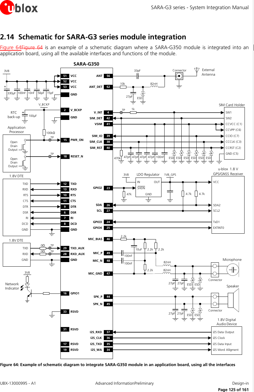
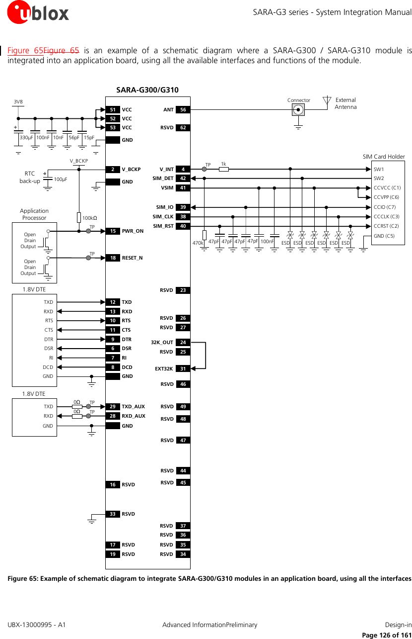
![SARA-G3 series - System Integration Manual UBX-13000995 - A1 Advanced InformationPreliminary Design-in Page 127 of 161 2.15 Design-in checklist This section provides a design-in checklist. 2.15.1 Schematic checklist The following are the most important points for a simple schematic check: DC supply must provide a nominal voltage at VCC pin above the minimum operating range limit. DC supply must be capable of providing 1.9 A current pulses, providing a voltage at VCC pin above the minimum operating range limit and with a maximum 400 mV voltage drop from the nominal value. VCC supply should be clean, with very low ripple/noise: provide the suggested bypass capacitors, in particular if the application device integrates an internal antenna. VCC voltage must ramp from 2.5 V to 3.2 V within 4 ms to allow a proper switch-on of the module. Do not leave PWR_ON floating: fix properly the level, e.g. adding a proper pull-up resistor to V_BCKP. Do not apply loads which might exceed the limit for maximum available current from V_INT supply. Check that voltage level of any connected pin does not exceed the relative operating range. Capacitance and series resistance must be limited on each SIM signal to match the SIM specifications. Insert the suggested capacitors on each SIM signal and low capacitance ESD protections if accessible. Check UART signals direction, since the signal names follow the ITU-T V.24 Recommendation [9]. Provide accessible testpoints directly connected to the following pins: TXD_AUX and RXD_AUX pins, V_INT pin, PWR_ON and/or RESET_N pins, to allow the module firmware upgrade using the u-blox EasyFlash tool and to allow the trace log capture (debug purpose). Add a proper pull-up resistor (e.g. 4.7 k ) to V_INT or another proper 1.8 V supply on each DDC (I2C) interface line, if the interface is used. Capacitance and series resistance must be limited on each line of the DDC (I2C) interface. Use transistors with at least an integrated resistor in the base pin or otherwise put a 10 k resistor on the board in series to the GPIO when those are used to drive LEDs. Connect the pin number 33 (RSVD) to ground. Insert the suggested passive filtering parts on each used analog audio line. Check the digital audio interface specifications to connect a proper device. Provide proper precautions for ESD immunity as required on the application board. Any external signal connected to the UART interface, auxiliary UART interface, I2S interfaces and GPIOs must be tri-stated or set low when the module is in power-down mode and during the module power-on sequence (at least until the activation of the V_INT supply output of the module), to avoid latch-up of circuits and let a proper boot of the module. All unused pins can be left unconnected except the PWR_ON pin (its level must be properly fixed, e.g. adding a 100 k pull-up to V_BCKP) and the RSVD pin number 33 (it must be connected to GND).](https://usermanual.wiki/u-blox/SARAG350.User-manual/User-Guide-2055502-Page-127.png)
![SARA-G3 series - System Integration Manual UBX-13000995 - A1 Advanced InformationPreliminary Handling and soldering Page 129 of 161 3 Handling and soldering No natural rubbers, no hygroscopic materials or materials containing asbestos are employed. 3.1 Packaging, shipping, storage and moisture preconditioning For information pertaining to reels and tapes, Moisture Sensitivity levels (MSD), shipment and storage information, as well as drying for preconditioning see the SARA-G3 series Data Sheet [1] and the u-blox Package Information Guide [24]. The SARA-G3 series modules are Electro-Static Discharge (ESD) sensitive devices. Ensure ESD precautions are implemented during handling of the module. 3.2 Soldering 3.2.1 Soldering paste Use of "No Clean" soldering paste is strongly recommended, as it does not require cleaning after the soldering process has taken place. The paste listed in the example below meets these criteria. Soldering Paste: OM338 SAC405 / Nr.143714 (Cookson Electronics) Alloy specification: 95.5% Sn / 3.9% Ag / 0.6% Cu (95.5% Tin / 3.9% Silver / 0.6% Copper) 95.5% Sn / 4.0% Ag / 0.5% Cu (95.5% Tin / 4.0% Silver / 0.5% Copper) Melting Temperature: 217 °C Stencil Thickness: 150 µm for base boards The final choice of the soldering paste depends on the approved manufacturing procedures. The paste-mask geometry for applying soldering paste should meet the recommendations in section 2.10 The quality of the solder joints on the connectors (’half vias’) should meet the appropriate IPC specification. 3.2.2 Reflow soldering A convection type-soldering oven is strongly recommended over the infrared type radiation oven. Convection heated ovens allow precise control of the temperature and all parts will be heated up evenly, regardless of material properties, thickness of components and surface color. Consider the "IPC-7530 Guidelines for temperature profiling for mass soldering (reflow and wave) processes, published 2001". Reflow profiles are to be selected according to the following recommendations. Failure to observe these recommendations can result in severe damage to the device!](https://usermanual.wiki/u-blox/SARAG350.User-manual/User-Guide-2055502-Page-129.png)
![SARA-G3 series - System Integration Manual UBX-13000995 - A1 Advanced InformationPreliminary Handling and soldering Page 130 of 161 Preheat phase Initial heating of component leads and balls. Residual humidity will be dried out. Note that this preheat phase will not replace prior baking procedures. Temperature rise rate: max 3 °C/s If the temperature rise is too rapid in the preheat phase it may cause excessive slumping. Time: 60 – 120 s If the preheat is insufficient, rather large solder balls tend to be generated. Conversely, if performed excessively, fine balls and large balls will be generated in clusters. End Temperature: 150 - 200 °C If the temperature is too low, non-melting tends to be caused in areas containing large heat capacity. Heating/ reflow phase The temperature rises above the liquidus temperature of 217 °C. Avoid a sudden rise in temperature as the slump of the paste could become worse. Limit time above 217 °C liquidus temperature: 40 - 60 s Peak reflow temperature: 245 °C Cooling phase A controlled cooling avoids negative metallurgical effects (solder becomes more brittle) of the solder and possible mechanical tensions in the products. Controlled cooling helps to achieve bright solder fillets with a good shape and low contact angle. Temperature fall rate: max 4 °C/s To avoid falling off, modules should be placed on the topside of the motherboard during soldering. The soldering temperature profile chosen at the factory depends on additional external factors like choice of soldering paste, size, thickness and properties of the base board, etc. Exceeding the maximum soldering temperature and the maximum liquidus time limit in the recommended soldering profile may permanently damage the module. Preheat Heating Cooling[°C] Peak Temp. 245°C [°C]250 250Liquidus Temperature217 217200 20040 - 60 sEnd Temp.max 4°C/s150 - 200°C150 150max 3°C/s60 - 120 s100 Typical Leadfree 100Soldering Profile50 50Elapsed time [s] Figure 66: Recommended soldering profile SARA-G3 series modules must not be soldered with a damp heat process.](https://usermanual.wiki/u-blox/SARAG350.User-manual/User-Guide-2055502-Page-130.png)
![SARA-G3 series - System Integration Manual UBX-13000995 - A1 Advanced InformationPreliminary Approvals Page 133 of 161 4 Approvals For the complete list of all the certification schemes approvals of SARA-G3 series modules and the corresponding declarations of conformity, refer to the u-blox web-site (http://www.u-blox.com). 4.1 Product certification approval overview Product certification approval is the process of certifying that a product has passed all tests and criteria required by specifications, typically called “certification schemes” that can be divided into three distinct categories: Regulatory certification o Country specific approval required by local government in most regions and countries, as: CE (Conformité Européenne) marking for European Union FCC (Federal Communications Commission) approval for United States Industry certification o Telecom industry specific approval verifying the interoperability between devices and networks: GCF (Global Certification Forum), partnership between European device manufacturers and network operators to ensure and verify global interoperability between devices and networks PTCRB (PCS Type Certification Review Board), created by United States network operators to ensure and verify interoperability between devices and North America networks Operator certification o Operator specific approval required by some mobile network operator, as: AT&T network operator in United States Even if SARA-G3 modules are approved under all major certification schemes, the application device that integrates SARA-G3 modules must be approved under all the certification schemes required by the specific application device to be deployed in the market. The required certification scheme approvals and relative testing specifications differ depending on the country or the region where the device that integrates SARA-G3 series modules must be deployed, on the relative vertical market of the device, on type, features and functionalities of the whole application device, and on the network operators where the device must operate. The certification of the application device that integrates a SARA-G3 module and the compliance of the application device with all the applicable certification schemes, directives and standards are the sole responsibility of the application device manufacturer. SARA-G3 modules are certified according to all capabilities and options stated in the Protocol Implementation Conformance Statement document (PICS) of the module. The PICS, according to 3GPP TS 51.010-2 [14], is a statement of the implemented and supported capabilities and options of a device. The PICS document of the application device integrating a SARA-G3 module must be updated from the module PICS statement if any feature stated as supported by the module in its PICS document is not implemented or disabled in the application device, as for the following cases: o if any RF band is disabled by AT+UBANDSEL command o if the automatic network attach is disabled by AT+COPS command o if the module’s GPRS multi-slot class is changed by AT+UCLASS command](https://usermanual.wiki/u-blox/SARAG350.User-manual/User-Guide-2055502-Page-133.png)
![SARA-G3 series - System Integration Manual UBX-13000995 - A1 Advanced InformationPreliminary Approvals Page 134 of 161 4.2 Federal Communications Commission and Industry Canada notice Federal Communications Commission (FCC) ID for the SARA-G3 series modules are: For SARA-G310 modules: XPYSARAG350 For SARA-G350 modules: XPYSARAG350 Industry Canada (IC) Certification Numbers for the SARA-G3 series modules are: For SARA-G310 modules: 8595A-SARAG350 For SARA-G350 modules: 8595A-SARAG350 4.2.1 Safety Warnings review the structure Equipment for building-in. The requirements for fire enclosure must be evaluated in the end product The clearance and creepage current distances required by the end product must be withheld when the module is installed The cooling of the end product shall not negatively be influenced by the installation of the module Excessive sound pressure from earphones and headphones can cause hearing loss No natural rubbers, no hygroscopic materials nor materials containing asbestos are employed 4.2.2 Declaration of Conformity – United States only This device complies with Part 15 of the FCC rules. Operation is subject to the following two conditions: this device may not cause harmful interference this device must accept any interference received, including interference that may cause undesired operation Radiofrequency radiation exposure Information: this equipment complies with FCC radiation exposure limits prescribed for an uncontrolled environment for fixed and mobile use conditions. This equipment should be installed and operated with a minimum distance of 20 cm between the radiator and the body of the user or nearby persons. This transmitter must not be co-located or operating in conjunction with any other antenna or transmitter except as authorized in the certification of the product. The gain of the system antenna(s) used for the SARA-G350 modules (i.e. the combined transmission line, connector, cable losses and radiating element gain) must not exceed 8.39 dBi (850 MHz) and 3.11 dBi (1900 MHz) for mobile and fixed or mobile operating configurations. 4.2.3 Modifications The FCC requires the user to be notified that any changes or modifications made to this device that are not expressly approved by u-blox could void the user's authority to operate the equipment. Manufacturers of mobile or fixed devices incorporating the SARA-G350 modules are authorized to use the FCC Grants and Industry Canada Certificates of the SARA-G350 modules for their own final products according to the conditions referenced in the certificates. The FCC Label shall in the above case be visible from the outside, or the host device shall bear a second label stating: For SARA-G310 modules: "Contains FCC ID: XPYSARAG310XPYSARAG350" resp. [TBD] For SARA-G350 modules: "Contains FCC ID: XPYSARAG350" resp. The IC Label shall in the above case be visible from the outside, or the host device shall bear a second label stating: For SARA-G310 modules: "Contains IC: 8595A-SARAG310SARAG350" resp. [TBD] Comment [smos1]: Can we change this to one line: For SARA-G310 and SARA-G350 modules: "Contains FCC ID: XPYSARAG350".](https://usermanual.wiki/u-blox/SARAG350.User-manual/User-Guide-2055502-Page-134.png)
![SARA-G3 series - System Integration Manual UBX-13000995 - A1 Advanced InformationPreliminary Approvals Page 135 of 161 For SARA-G350 modules: "Contains IC: 8595A-SARAG350" resp. Canada, Industry Canada (IC) Notices This Class B digital apparatus complies with Canadian CAN ICES-3 (B)/NMB-3(B)ICES-003 and RSS-210. Operation is subject to the following two conditions: o this device may not cause interference o this device must accept any interference, including interference that may cause undesired operation of the device Radio Frequency (RF) Exposure Information The radiated output power of the u-blox Wireless Module is below the Industry Canada (IC) radio frequency exposure limits. The u-blox Wireless Module should be used in such a manner such that the potential for human contact during normal operation is minimized. This device has been evaluated and shown compliant with the IC RF Exposure limits under mobile exposure conditions (antennas are greater than 20cm from a person's body). This device has been certified for use in Canada. Status of the listing in the Industry Canada’s REL (Radio Equipment List) can be found at the following web address: http://www.ic.gc.ca/app/sitt/reltel/srch/nwRdSrch.do?lang=eng Additional Canadian information on RF exposure also can be found at the following web address: http://www.ic.gc.ca/eic/site/smt-gst.nsf/eng/sf08792.html IMPORTANT: Manufacturers of portable applications incorporating the SARA-G310 / SARA-G350 modules are required to have their final product certified and apply for their own FCC Grant and Industry Canada Certificate related to the specific portable device. This is mandatory to meet the SAR requirements for portable devices. Changes or modifications not expressly approved by the party responsible for compliance could void the user's authority to operate the equipment. Canada, avis d'Industrie Canada (IC) Cet appareil numérique de classe B est conforme aux normes canadiennes ICES-003CAN ICES-3 (B)/NMB-3(B) et RSS-210. Son fonctionnement est soumis aux deux conditions suivantes: o cet appareil ne doit pas causer d'interférence o cet appareil doit accepter toute interférence, notamment les interférences qui peuvent affecter son fonctionnement Informations concernant l'exposition aux fréquences radio (RF) La puissance de sortie émise par l’appareil de sans fil u-blox Wireless Module est inférieure à la limite d'exposition aux fréquences radio d'Industrie Canada (IC). Utilisez l’appareil de sans fil u-blox Wireless Module de façon à minimiser les contacts humains lors du fonctionnement normal. Ce périphérique a été évalué et démontré conforme aux limites d'exposition aux fréquences radio (RF) d'IC lorsqu'il est installé dans des produits hôtes particuliers qui fonctionnent dans des conditions d'exposition à des appareils mobiles (les antennes se situent à plus de 20 centimètres du corps d'une personne). Ce périphérique est homologué pour l'utilisation au Canada. Pour consulter l'entrée correspondant à l’appareil dans la liste d'équipement radio (REL - Radio Equipment List) d'Industrie Canada rendez-vous sur: http://www.ic.gc.ca/app/sitt/reltel/srch/nwRdSrch.do?lang=fra Pour des informations supplémentaires concernant l'exposition aux RF au Canada rendez-vous sur: http://www.ic.gc.ca/eic/site/smt-gst.nsf/eng/sf08792.html IMPORTANT: les fabricants d'applications portables contenant les modules SARA-G310 / SARA--G350 doivent faire certifier leur produit final et déposer directement leur candidature pour une Comment [smos2]: Can we change this to one line: For SARA-G310 and SARA-G350 modules: "Contains IC: 8595A-SARAG350". Field Code ChangedField Code Changed](https://usermanual.wiki/u-blox/SARAG350.User-manual/User-Guide-2055502-Page-135.png)
![SARA-G3 series - System Integration Manual UBX-13000995 - A1 Advanced InformationPreliminary Approvals Page 138 of 161 The temperature range for using SARA-G350 ATEX modules is defined in the ‘Operating temperature range’ section of the SARA-G3 series Data Sheet [1]. The RF radiating profile of SARA-G350 ATEX modules is compliant to all the applicable 3GPP / ETSI standards, with a maximum of 2 W RF pulse power and 1.15 mJ RF pulse energy according to the GSM/GPRS power class stated in Table 2Table 2. The nameplate of SARA-G350 ATEX modules is described in the ‘Product labeling’ section of the SARA-G3 series Data Sheet [1]. The following maximum input and equivalent parameters must be considered in sub-division IIC: Ui = 3.8 V Ii = 1.6 A (burst) Pi = 2.5 W Ci = 103 µF Li = 4.1 µH The following maximum input and equivalent parameters must be considered in sub-divisions IIB, IIA: Ui = 4.2 V Ii = 2.5 A (burst) Pi = 2.5 W Ci = 103 µF Li = 4.1 µH](https://usermanual.wiki/u-blox/SARAG350.User-manual/User-Guide-2055502-Page-138.png)
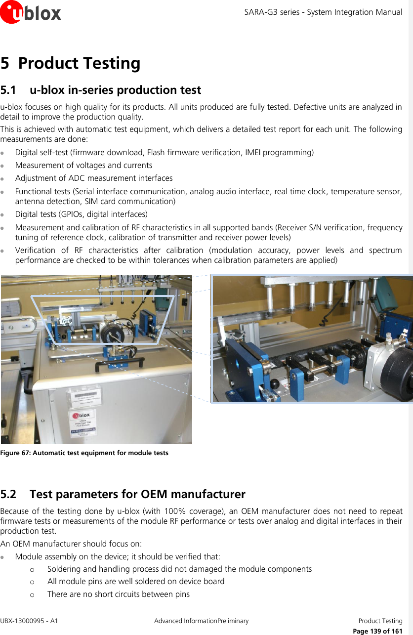
![SARA-G3 series - System Integration Manual UBX-13000995 - A1 Advanced InformationPreliminary Product Testing Page 140 of 161 Component assembly on the device; it should be verified that: o Communication with host controller can be established o The interfaces between module and device are working o Overall RF performance test of the device including antenna Dedicated tests can be implemented to check the device. For example, the measurement of module current consumption when set in a specified status can detect a short circuit if compared with a “Golden Device” result. Module AT commands are used to perform functional tests (communication with host controller, check SIM card interface, check communication between module and GPS/GNSS, GPIOs, etc.) and to perform RF performance tests. 5.2.1 “Go/No go” tests for integrated devices A ‘Go/No go’ test is to compare the signal quality with a “Golden Device” in a position with excellent network coverage and after having dialed a call (refer to u-blox AT Commands Manual [2], AT+CSQ command: <rssi>, <ber> parameters). These kinds of test may be useful as a ‘go/no go’ test but not for RF performance measurements. This test is suitable to check the communication with host controller and SIM card, the audio and power supply functionality and verify if components at antenna interface are well soldered. 5.2.2 Functional tests providing RF operation Overall RF performance test of the device including antenna can be performed with basic instruments such as a spectrum analyzer (or an RF power meter) and a signal generator using AT+UTEST command over AT interface. The AT+UTEST command gives a simple interface to set the module to Rx and Tx test modes ignoring GSM/GPRS signaling protocol. The command can set the module: In transmitting mode in a specified channel and power level in all supported modulation schemes (single slot GMSK) and bands In receiving mode in a specified channel to returns the measured power level in all supported bands Refer to the u-blox AT Commands Manual [2], for AT+UTEST command syntax description. Refer to the End user test Application Note [23], for AT+UTEST command user guide, limitations and examples of use.](https://usermanual.wiki/u-blox/SARAG350.User-manual/User-Guide-2055502-Page-140.png)
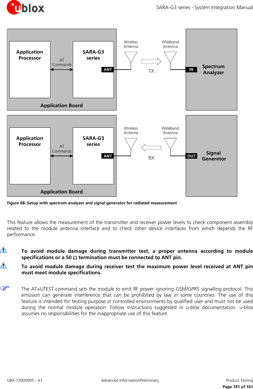
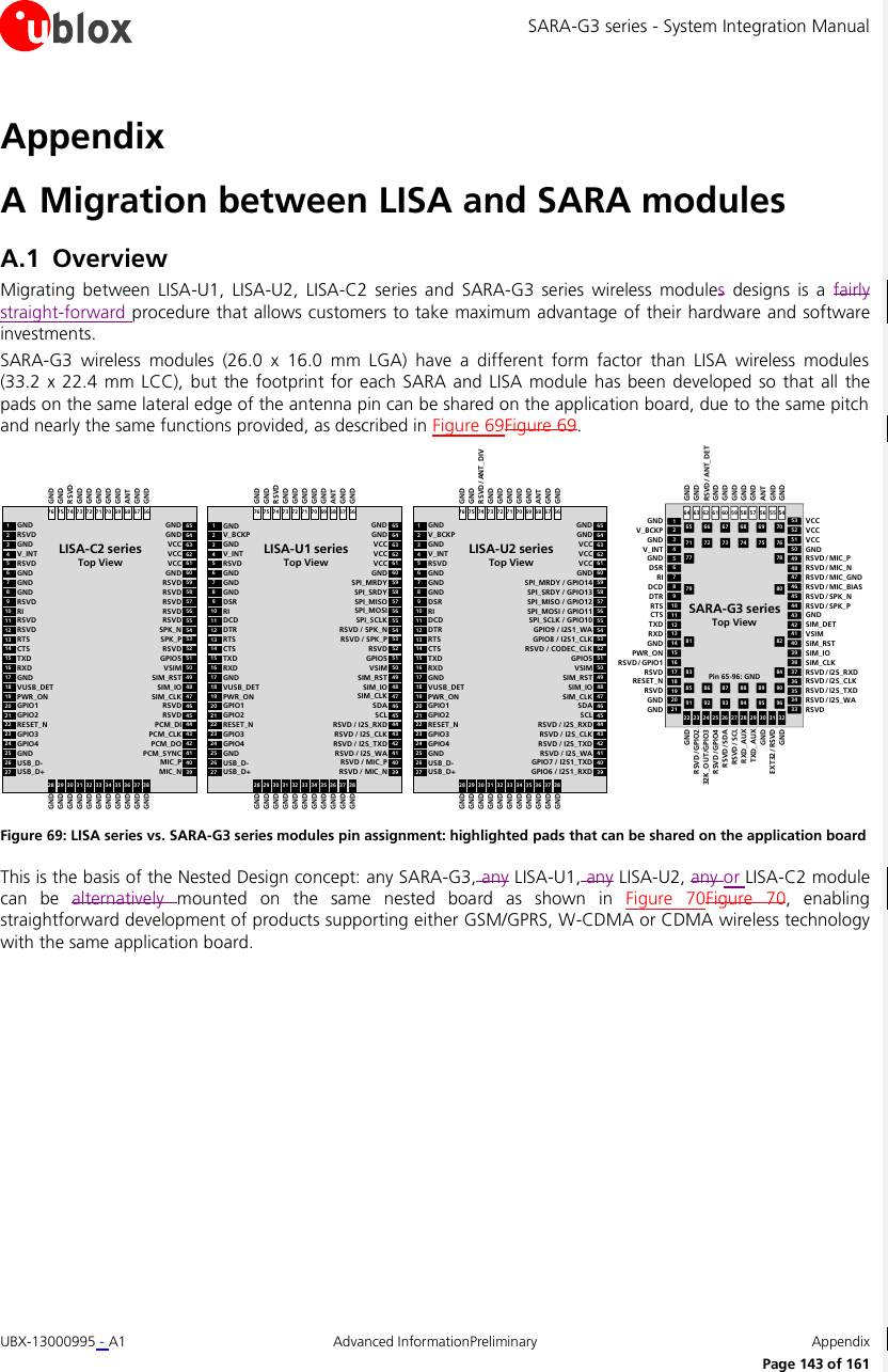
![SARA-G3 series - System Integration Manual UBX-13000995 - A1 Advanced InformationPreliminary Appendix Page 144 of 161 LISANESTED APPLICATION BOARDTop Layer and Solder MaskLISA mounting optionwith LISA Paste MaskSARASARA mounting optionwith SARA Paste MaskANT pad Figure 70: Nested Design concept description: LISA and SARA modules alternatively mounted on the same application board The voltage level of all the digital interfaces of SARA-G3 and LISA modules is 1.8 V: this allows the direct connection from a 1.8 V external device (e.g. application processor) to all the modules. The following sections explains in details all the points to consider during the migration between LISA and SARA designs, implementing or not a nested design For further details regarding SARA-G3 and LISA modules characteristics, usage, or settings, refer to the relative relevant module datasheet [1], [3], [4], [5], System Integration Manual [6], [7], and AT commands manual [2], [8]. A.2 Checklist for migration Have you chosen the optimal SARA-G3 series module? For quad-band GSM/GPRS, full feature set, select the SARA-G350 module. For quad-band GSM/GPRS, reduced feature set, select the SARA-G310 module. For dual-band GSM/GPRS, reduced feature set, select the SARA-G300 module. Check SARA-G3 series modules hardware requirements Check power capabilities of the external supply circuit: SARA-G3 modules require large current pulses in connected-mode as well as LISA-U series modules when a 2G call is enabled. LISA-C2 series modules do not require large current pulses due to the CDMA channel access technology. Check supported bands for proper antenna circuit development: SARA-G3 modules frequency ranges are within LISA-U modules ranges, but LISA-C2 modules range is quite different. Check antenna detection requirements: SARA-G350 modules provide the antenna detection function implementing an external application circuit between ANT_DET and ANT pins. Check the module power-on requirements: Table 41Table 41 and relative section summarize differences between SARA-G3 series and LISA modules. Check the module requirements to enter low power idle-mode: SARA-G300 and SARA-G310 modules require a 32 kHz signal at EXT32K input, which for example can be provided by the 32K_OUT output. Check serial interfaces requirements: SARA-G3 modules provide UART interface for AT command, data communication, multiplexer functionality, FW upgrade over AT and provide auxiliary UART interface for FW upgrade using the u-blox EasyFlash tool and for Trace log capture (debug purpose). Check analog audio requirements: SARA-G350 modules do not provide DC blocking capacitors at the MIC_P / MIC_N input pins and provide supply output and local ground for an external microphone at the MIC_BIAS / MIC_GND pins.](https://usermanual.wiki/u-blox/SARAG350.User-manual/User-Guide-2055502-Page-144.png)
![SARA-G3 series - System Integration Manual UBX-13000995 - A1 Advanced InformationPreliminary Appendix Page 146 of 161 A.3 Software migration Software migration between SARA-G3 and LISA wireless modules is a straightforward procedure. Nevertheless there are some differences to be considered with firmware version. Each wireless module supports AT commands according to 3GPP standards: TS 27.007 [10], TS 27.005 [11], TS 27.010 [12] and the u-blox AT command extension. Backward compatibility has been maintained as far as possible. For the complete list of supported AT commands and their syntax refer to the relativerefer to the relevant AT commands manual of the module [2], [8]. A.4 Hardware migration SARA-G3 series modules have been designed with backward compatibility to LISA series modules in mind but some minor differences were unavoidable. These minor differences are however not relevant for the majority of the designs. The following subsections describe the hardware differences between the interfaces of SARA-G3 series modules and LISA series modules while Table 42Table 42 summarizes the detailed differences between the pins. A.4.1 Supply interfaces Module supply input (VCC) The same compatible external circuit can be implemented for SARA-G3 and LISA even if there are minor differences in the VCC input voltage ranges and some differences in the current consumption figures. The voltage provided must be within the normal operating range limits to allow module switch-on and must be above the minimum limit of the extended operating range to avoid module switch-off. For the detailed VCC input voltage ranges values refer to Table 42Table 42 or to the relative datasheet of the module [1], [3], [4], [5]. The SARA-G3 maximum average current consumption is lower than the LISA one due to the lower data rate or the different channel access technology. SARA-G3 modules require large current pulses in connected-mode as well as LISA-U series when a 2G call is enabled. LISA-C2 series do not require large current pulses due to the CDMA channel access technology. For the detailed current consumption values refer to the relativerefer to the relevant module datasheet of the module [1], [3], [4], [5]. Detailed supply circuit design-in guidelines are reported in section 2.1.1 and in the relative System Integration Manual of the module [6], [7]. RTC supply input/output (V_BCKP) The same compatible external circuit can be implemented for SARA-G3 series and LISA-U series even if there are minor differences in the V_BCKP typical output voltage and input voltage range as reported in Table 42Table 42 or in the relative datasheet of the module [1], [3], [4], [5]. LISA-C2 series do not provide V_BCKP RTC supply input/output as well as the whole RTC functionality. Interfaces supply output (V_INT) The same compatible external circuit can be implemented for SARA-G3 series and LISA series: there are no differences in the V_INT output characteristics.](https://usermanual.wiki/u-blox/SARAG350.User-manual/User-Guide-2055502-Page-146.png)
![SARA-G3 series - System Integration Manual UBX-13000995 - A1 Advanced InformationPreliminary Appendix Page 147 of 161 A.4.2 System functions interfaces Module power-on SARA-G3 and LISA series power-on sequence is initiated in one of the ways summarized in Table 41Table 41. For more details, refer to section 1.6.1 or to the relative System Integration Manual of the module [6], [7]. SARA-G3 series LISA-C2 series LISA-U1 series LISA-U2 series Rising edge on the VCC pins to a valid voltage as module supply Rising edge on the VCC pins to a valid voltage as module supply with PWR_ON pin permanently low when VCC is applied Rising edge on the VCC pins to a valid voltage as module supply Rising edge on the VCC pins to a valid voltage as module supply Low level on the PWR_ON pin for appropriate time period Low pulse on the PWR_ON pin for appropriate time period Low pulse on the PWR_ON pin for appropriate time period Low pulse on the PWR_ON pin for appropriate time period Pre-programmed RTC alarm (external 32 kHz at EXT32K needed for SARA-G300/G310) Pre-programmed RTC alarm Pre-programmed RTC alarm RESET_N input pin released from the low level RESET_N input pin released from the low level Table 41: Summary of power on events among modules The same compatible external power-on circuit can be implemented for SARA-G3 series and LISA series even if there are minor differences in the PWR_ON input voltage levels ranges and in the low level time or low pulse time to switch-on the module, as reported in Table 42Table 42 or in the relative datasheet of the module [1], [3], [4], [5]. PWR_ON falling edge (i.e. low pulse) is required for LISA series, but it is not required for SARA-G3 series. External pull-up is not needed for LISA-C2 series since internal pull-up is provided. Module power-off SARA-G3 and LISA modules can all be all properly switched off by means of the AT+CPWROFF command. Additionally, Aall LISA-U2 modules, except LISA-U200-00S, modules can be additionally properly switched off by low pulse on the PWR_ON pin, as reported in Table 42Table 42 or in the relative datasheet of the module [5]. Module reset SARA-G3 series and LISA series modules reset can be performed in one of the following ways: Forcing a low level on the RESET_N pin, causing an “external” or “hardware” reset By means of the AT+CFUN command, causing an “internal” or “software” reset The same compatible external reset circuit can be implemented for SARA-G3 series and LISA series even if there are minor differences in the RESET_N input voltage levels ranges and in the low level time, as reported in Table 42Table 42 or in the relative datasheet of the module [1], [3], [4], [5]. Additional precautions are suggested for the RESET_N line of LISA-U series modules, depending on the application board handling, to satisfy ESD immunity test requirements as described in the LISA-U Series System Integration Manual [7]. External 32 kHz input and internal 32 kHz output The EXT32K input and the 32K_OUT output are available only on the SARA-G300 and SARA-G310 modules to provide the 32 kHz reference clock for the Real Time Clock (RTC) timing, used by the module processor to reach the low power idle-mode and provide the RTC functions. SARA-G350 and LISA-U modules are equipped with internal 32 kHz oscillator to provide the same functions. LISA-C2 series do not provide RTC and the relative functions.](https://usermanual.wiki/u-blox/SARAG350.User-manual/User-Guide-2055502-Page-147.png)
![SARA-G3 series - System Integration Manual UBX-13000995 - A1 Advanced InformationPreliminary Appendix Page 148 of 161 A.4.3 Antenna interface RF interface for Tx/Rx antenna The same compatible external circuit can be implemented for SARA-G3 series and LISA series ANT pin even if there are some differences in the operating bands frequency ranges, as summarized in Figure 71Figure 71. VV II II850900850800 850 900 950900 18001900 190018001700 1750 1800 1850 1900 1950 2000 2050 2100 2150 2200824 960 1710 1990LISA-U100 LISA-U120 LISA-U260LISA-U200 LISA-U230VV II II850900850800 850 900 950900 18001900 190018001700 1750 1800 1850 1900 1950 2000 2050 2100 2150 2200IIVIVIVIIIVIII IV IV824 960 1710 2170850900850800 850 900 950900 18001900 190018001700 1750 1800 1850 1900 1950 2000 2050 2100 2150 2200IIVIIIVIII824 960 1710 2170LISA-U110 LISA-U130 LISA-U270850900850800 850 900 950900 18001900 190018001700 1750 1800 1850 1900 1950 2000 2050 2100 2150 2200824 960 1710 1990SARA-G310 SARA-G350900800 850 900 950900 1800 18001700 1750 1800 1850 1900 1950 2000 2050 2100 2150 2200880 960 1710 1880SARA-G300800800800 850 900 9501900 19001700 1750 1800 1850 1900 1950 2000 2050 2100 2150 2200824 894 1850 1990LISA-C200 Figure 71: Summary of operating bands frequency ranges among modules An external application circuit can be implemented on the application device integrating LISA-U2 series modules to satisfy ESD immunity test requirements at the antenna port, as described in the LISA-U Series System Integration Manual [7]. The same application circuit is not applicable for SARA-G3 series, LISA-U1 series and LISA-C2 series. RF interface for Rx diversity antenna Only the LISA-U230 modules provide the RF input for Rx diversity antenna (ANT_DIV). SARA-G3, LISA-C2, LISA-U1 and the other LISA-U2 series modules do not support Rx diversity. Antenna detection interface An external application circuit can be implemented on the application device integrating SARA-G350 modules to provide antenna detection functionality, with a proper connection between the ANT_DET pin and the ANT pin, as described in section 2.3.2. LISA-U modules are equipped with internal circuit for antenna detection support. SARA-G300, SARA-G310 and LISA-C2 series modules do not support antenna detection.](https://usermanual.wiki/u-blox/SARAG350.User-manual/User-Guide-2055502-Page-148.png)
![SARA-G3 series - System Integration Manual UBX-13000995 - A1 Advanced InformationPreliminary Appendix Page 149 of 161 A.4.4 SIM interface SIM interface The same compatible external circuit can be implemented for SARA-G3 and LISA modules: 1.8 V and 3.0 V SIM card / IC are supported. LISA-C2 modules do not need an external SIM for Sprint and Verizon mobile operators. LISA-C2 series SIM interface is hardware ready but the support of external SIM card / IC will be provided by the upcoming firmware releases. SIM detection interface The same compatible external circuit can be implemented for SARA-G3 and LISA modules: SIM detection function is provided by the SIM_DET pin on SARA-G3 modules and by the GPIO5 pin on LISA-U modules. SIM card hot insertion/removal is additionally supported by all LISA-U2 series except LISA-U200-00S. LISA-C2 modules do not support SIM detection. A.4.5 Serial interfaces UART interface The same compatible external circuit can be implemented for SARA-G3 and LISA modules: A 1.8 V unbalanced asynchronous serial port with RS-232 functionality is provided on SARA-G3 modules (for AT command, data communication, MUX functionality, FW upgrade over AT), LISA-C2 modules (for AT command, data communication, MUX functionality), LISA-U modules (for AT command, data communication, MUX functionality, FW upgrade over AT or using the u-blox EasyFlash tool). LISA-C2 modules do not support DSR, DCD and DTR functions. Table 42Table 42 and in relativethe module’s datasheet of the module [1], [3], [4], [5] report minor differences in the internal pull-ups and drivers strengths. These are the default settings of the UART interfaces: SARA-G3 modules: automatic baud rate and frame format detection LISA-U2 except LISA-U200-00S modules: one-shot automatic baud rate and frame format detection LISA-C2, LISA-U1 and LISA-U200-00S modules: 115200 b/s baud rate and 8N1 frame format For further details regarding UART interface settings refer to the relativemodule’s datasheet of the module [1], [3], [4], [5] and to the relative relevant AT commands manual of the module [2], [8]. UART AUX interface Only the SARA-G3 modules provide an auxiliary UART interface for FW upgrade using the u-blox EasyFlash tool and for Trace log capture (debug purpose). LISA modules do not provide an auxiliary UART interface. USB interface SARA-G3 modules do not provide a USB interface such asthat is available on LISA-U modules (High-Speed USB 2.0 for AT command, data communication, FW upgrade over AT or using the u-blox EasyFlash tool, and for Trace log capture) and on LISA-C2 modules (Full-Speed USB 2.0 for AT command, Data communication, FW upgrade). SPI interface SARA-G3 and LISA-C2 modules do not provide an SPI interface such asthat is available on LISA-U modules (5-wire IPC interface for AT command, data communication, MUX functionality, FW upgrade over AT). DDC (I2C) interface The same compatible external circuit can be implemented for SARA-G350 and LISA series: A 1.8 V DDC (I2C bus compatible) interface is provided to communicate with u-blox GPS/GNSS receivers.](https://usermanual.wiki/u-blox/SARAG350.User-manual/User-Guide-2055502-Page-149.png)
![SARA-G3 series - System Integration Manual UBX-13000995 - A1 Advanced InformationPreliminary Appendix Page 150 of 161 SARA-G300, SARA-G310 and LISA-U200-00S modules do not support the DDC (I2C) interface. LISA-C2 modules will support the DDC (I2C) interface byin the upcoming firmware releases. All LISA-U2 modules, except LISA-U200-00S, modules additionally support the communication with I2C slaves by means of dedicated AT commands, other then than u-blox positioning receivers over the same DDC (I2C) interface, by means of dedicated AT commands. A.4.6 Audio interfaces Analog audio interfaces Differential analog audio input is provided on the MIC_P / MIC_N pins of SARA-G350 modules (without internal DC blocking capacitor) and LISA-C2 series, LISA-U120, and LISA-U130 modules (with an internal DC blocking capacitor). Supply output and local ground for an external microphone is provided on the MIC_BIAS / MIC_GND pins of SARA-G350 modules only: the supply for an external microphone has to be provided by an external LDO linear regulator with the other modules. Differential analog audio output is provided on the SPK_P / SPK_N pins of SARA-G350, LISA-U120, LISA-U130 modules (16 ohm load capable) and LISA-C2 series modules (32 ohm load capable). SARA-G300/G310, LISA-U100/U110, LISA-U200-00S modules do not provide analog audio interfaces. LISA-U2 series modules do not provide analog audio interfaces, but analog audio can be provided with external audio codec connected to a digital audio interface of all LISA-U2 series modules except LISA-U200-00S modules (e.g. the 4-wire I2S digital audio interface provided instead of the 4 analog audio pins). The modules provide control of the external codec by means of the I2C interface and clock reference by means of the CODEC_CLK pin. For further details regarding analog audio interfaces characteristics, usage, and settings, refer to the relativerefer to the relevant module datasheet [1], [3], [4], [5], System Integration Manual 1.10.1, 2.6.1, [6], [7], and AT commands manual [2], [8]. Digital audio interfaces The dDigital audio interface is provided on the I2S_TXD, I2S_RXD, I2S_CLK, I2S_WA pins of SARA-G350 modules (1.8 V, PCM & Normal I2S modes, master, fixed sample rate) and LISA-U120/U130 and all LISA-U2 series modules except LISA-U200-00S modules (1.8 V, PCM & Normal I2S modes, master & slave, configurable sample rate)., and iIt is provided on the PCM_DO, PCM_DI, PCM_CLK, PCM_SYNC pins of LISA-C2 series modules (1.8 V, PCM): t. The same compatible external circuit can be implemented according to external digital audio device capabilities. An additional digital audio interface is provided on I2S1_TXD, I2S1_RXD, I2S1_CLK, I2S1_WA pins of all LISA--U2 series except LISA-U200-00S (1.8 V, PCM & Normal I2S modes, master & slave, configurable sample rate). SARA-G300/G310, LISA-U100/U110, LISA-U200-00S modules do not provide digital audio interfaces. For further details regarding digital audio interfaces characteristics, usage, and settings, refer to the relativerefer to the relevant module datasheet [1], [3], [4], [5], System Integration Manual 1.10.2, 2.6.2, [6], [7], and AT commands manual [2], [8]. A.4.7 GPIO pins The same compatible external circuit can be implemented for SARA-G350 and LISA series: four 1.8 V GPIOs are provided by SARA-G350 modules, providing the same functionalities as LISA series modules except Module Status and Operating Mode Indications. SIM detection function is provided by tThe SIM_DET pin provides the SIM detection function on SARA-G3 series modules instead ofrather than the GPIO5 pin as on LISA-U series modules. SARA-G300 and SARA-G310 modules do not provide GPIOs.](https://usermanual.wiki/u-blox/SARAG350.User-manual/User-Guide-2055502-Page-150.png)
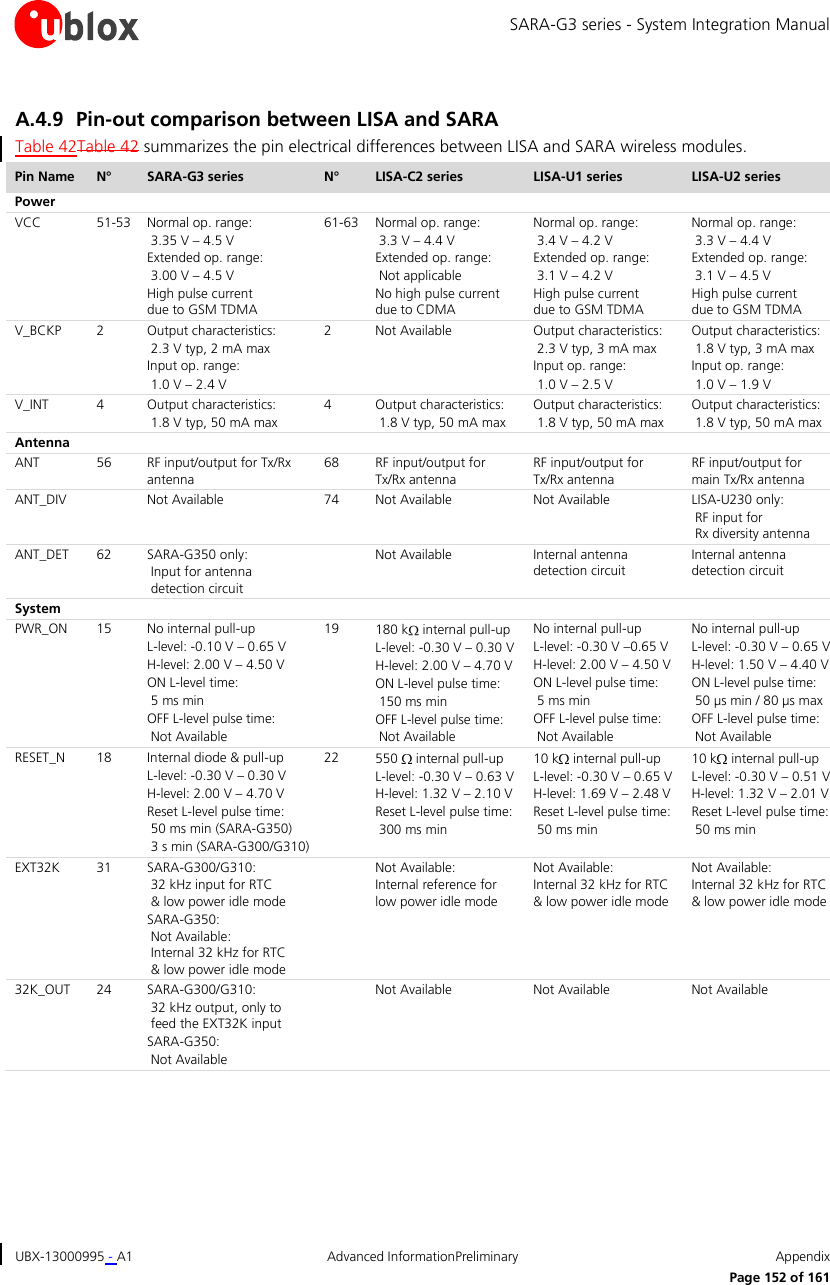
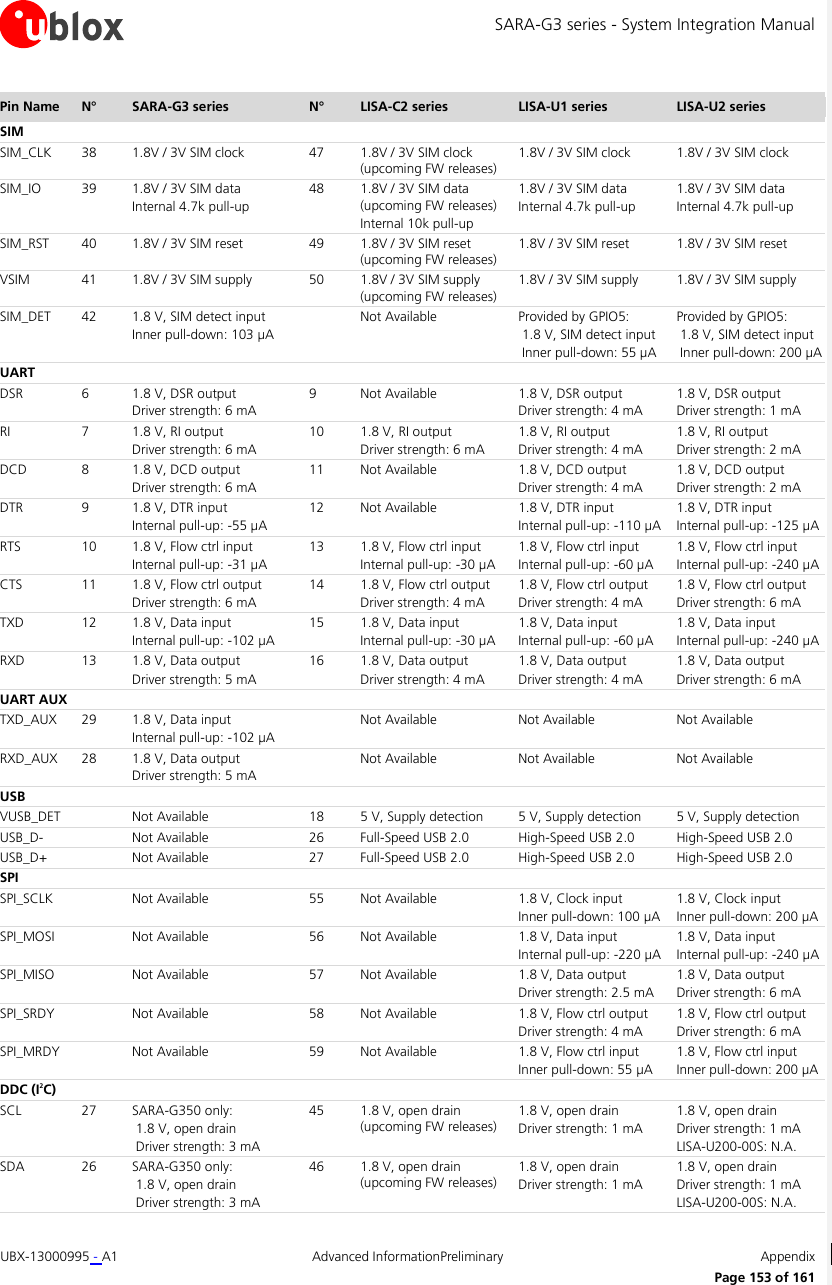
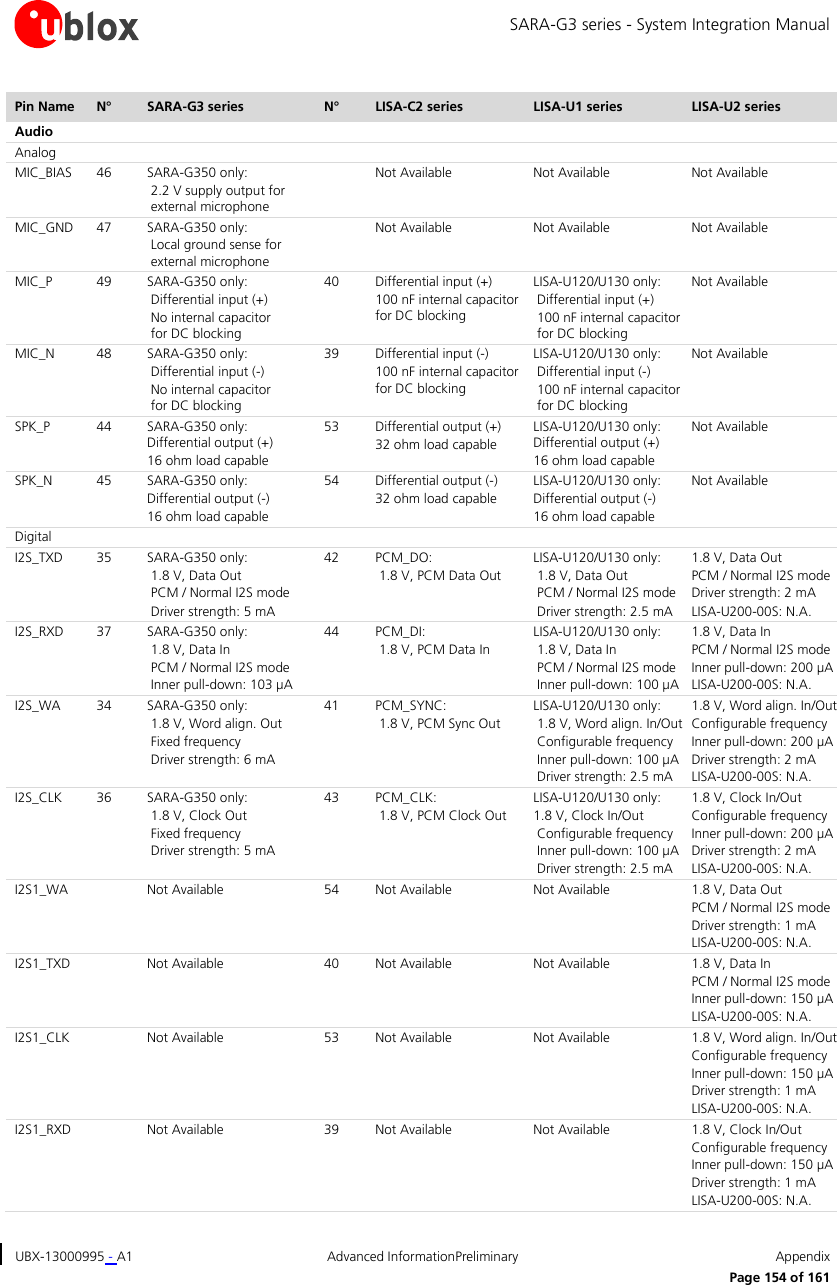
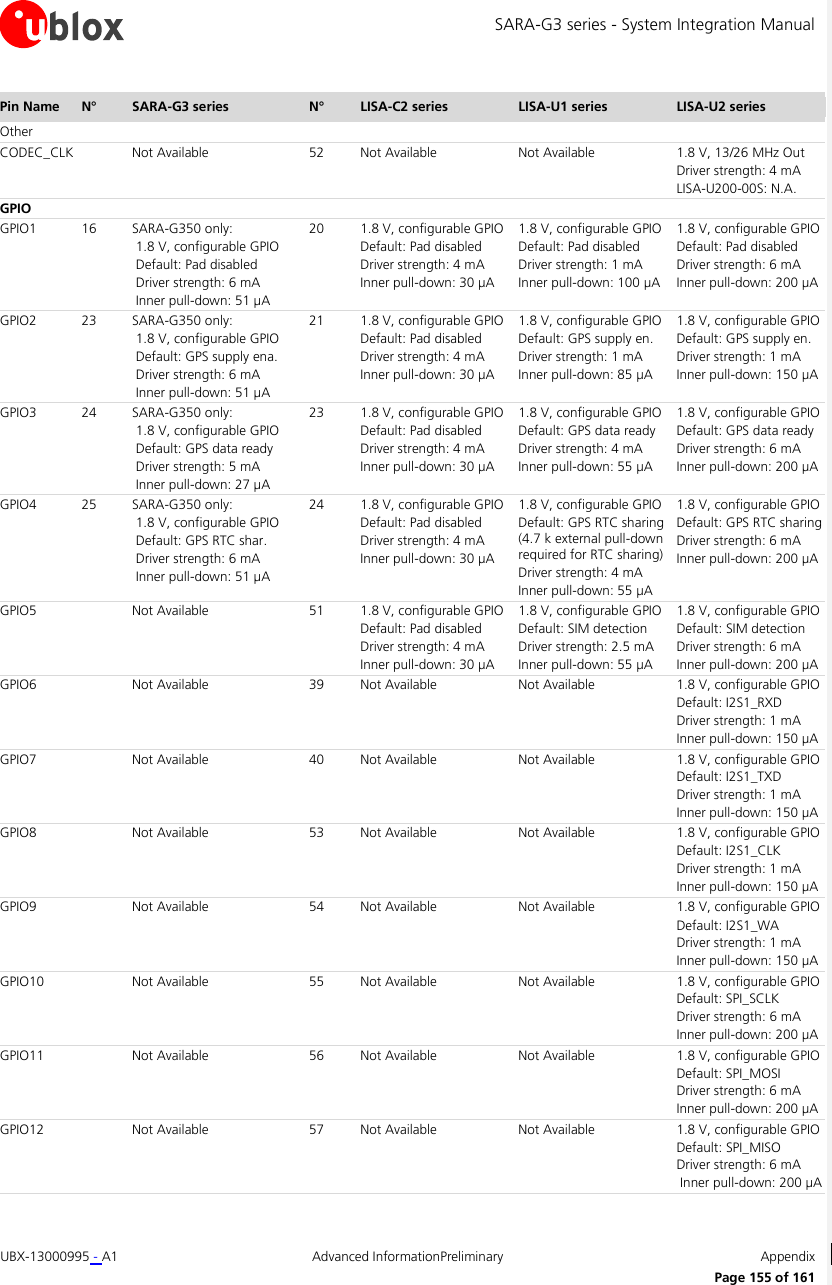
![SARA-G3 series - System Integration Manual UBX-13000995 - A1 Advanced InformationPreliminary Related documents Page 159 of 161 Related documents [1] u-blox SARA-G3 series Data Sheet, Docu No GSM.G2-HW-12001 [2] u-blox AT Commands Manual, Docu No WLS-SW-11000 [3] u-blox LISA-C200 series Data Sheet, Docu No CDMA-2X-11001 [4] u-blox LISA-U1 series Data Sheet, Docu No 3G.G2-HW-10001 [5] u-blox LISA-U2 series Data Sheet, Docu No 3G.G3-HW-11004 [6] u-blox LISA-C200 & FW75-C200 System Integration Manual, Docu No CDMA-2X-11004 [7] u-blox LISA-U series System Integration Manual, Docu No 3G.G2-HW-10002 [8] u-blox C200 AT Commands Manual, Docu No CDMA-2X-11002 [9] ITU-T Recommendation V.24 - 02-2000 - List of definitions for interchange circuits between the Data Terminal Equipment (DTE) and the Data Circuit-terminating Equipment (DCE). http://www.itu.int/rec/T-REC-V.24-200002-I/en [10] 3GPP TS 27.007 – AT command set for User Equipment (UE) (Release 1999) [11] 3GPP TS 27.005 – Use of Data Terminal Equipment – Data Circuit terminating; Equipment (DTE – DCE) interface for Short Message Service (SMS) and Cell Broadcast Service (CBS) (Release 1999) [12] 3GPP TS 27.010 – Terminal Equipment to User Equipment (TE-UE) multiplexer protocol (Release 1999) [13] I2C-Bus Specification Version 2.1 Philips Semiconductors (January 2000), http://www.nxp.com/acrobat_download/literature/9398/39340011_21.pdf [14] 3GPP TS 51.010-2 – Technical Specification Group GSM/EDGE Radio Access Network; Mobile Station (MS) conformance specification; Part 2: Protocol Implementation Conformance Statement (PICS) [15] CENELEC EN 61000-4-2 (2001): "Electromagnetic compatibility (EMC) – Part 4-2: Testing and measurement techniques – Electrostatic discharge immunity test". [16] ETSI EN 301 489-1 V1.8.1: “Electromagnetic compatibility and Radio spectrum Matters; EMC standard for radio equipment and services; Part 1: Common technical requirements” [17] ETSI EN 301 489-7 V1.3.1 “Electromagnetic compatibility and Radio spectrum Matters; EMC standard for radio equipment and services; Part 7: Specific conditions for mobile and portable radio and ancillary equipment of digital cellular radio telecommunications systems (GSM and DCS)“ [18] ETSI EN 301 489-24 V1.4.1 "Electromagnetic compatibility and Radio spectrum Matters; EMC standard for radio equipment and services; Part 24: Specific conditions for IMT-2000 CDMA Direct Spread (UTRA) for Mobile and portable (UE) radio and ancillary equipment" [19] 3GPP TS 26.267 V10.0.0 – eCall Data Transfer; In-band modem solution; General description (Rel. 10) [20] Multiplexer Implementation Application Note, Docu No WLS-CS-11002 [21] GPS Implementation Application Note, Docu No GSM.G1-CS-09007 [22] Firmware Update Application Note, Docu No WLS-CS-11001 [23] End user test Application Note, Docu No WLS-CS-12002 [24] u-blox Package Information Guide, Docu No GPS-X-11004 [25] BS EN 16062:2011 – Intelligent transport systems – eSafety – eCall high level application requirements [26] ETSI TS 122 101 V8.7.0 – Service aspects; Service principles (3GPP TS 22.101 v.8.7.0 Rel. 8) [27] IEC 60079-0 - Explosive atmospheres, Part 0: Equipment general requirements - 2011-06 [28] IEC 60079-11 - Explosive atmospheres, Part 11: Equipment protection by intrinsic safety 'i' - 2011-06 [29] IEC 60079-26 - Explosive atmospheres, Part 26: Equipment with EPL Ga - 2006-08 Some of the above documents can be downloaded from u-blox web-site (http://www.u-blox.com).](https://usermanual.wiki/u-blox/SARAG350.User-manual/User-Guide-2055502-Page-159.png)