Acer orporated N300 PDA with WLAN and Bluetooth User Manual Bluetooth manual
Acer Incorporated PDA with WLAN and Bluetooth Bluetooth manual
UserManual.wiki
>
Acer orporated
>
N300 User Manual
>
Bluetooth manual
Contents
1.
Users Manual
2.
Bluetooth manual
3.
WLAN manual
Bluetooth manual
Navigation menu
Upload a User Manual
Namespaces
Wiki Guide
HTML
PDF
Info
Views
User Manual
Discussion / Help
Navigation
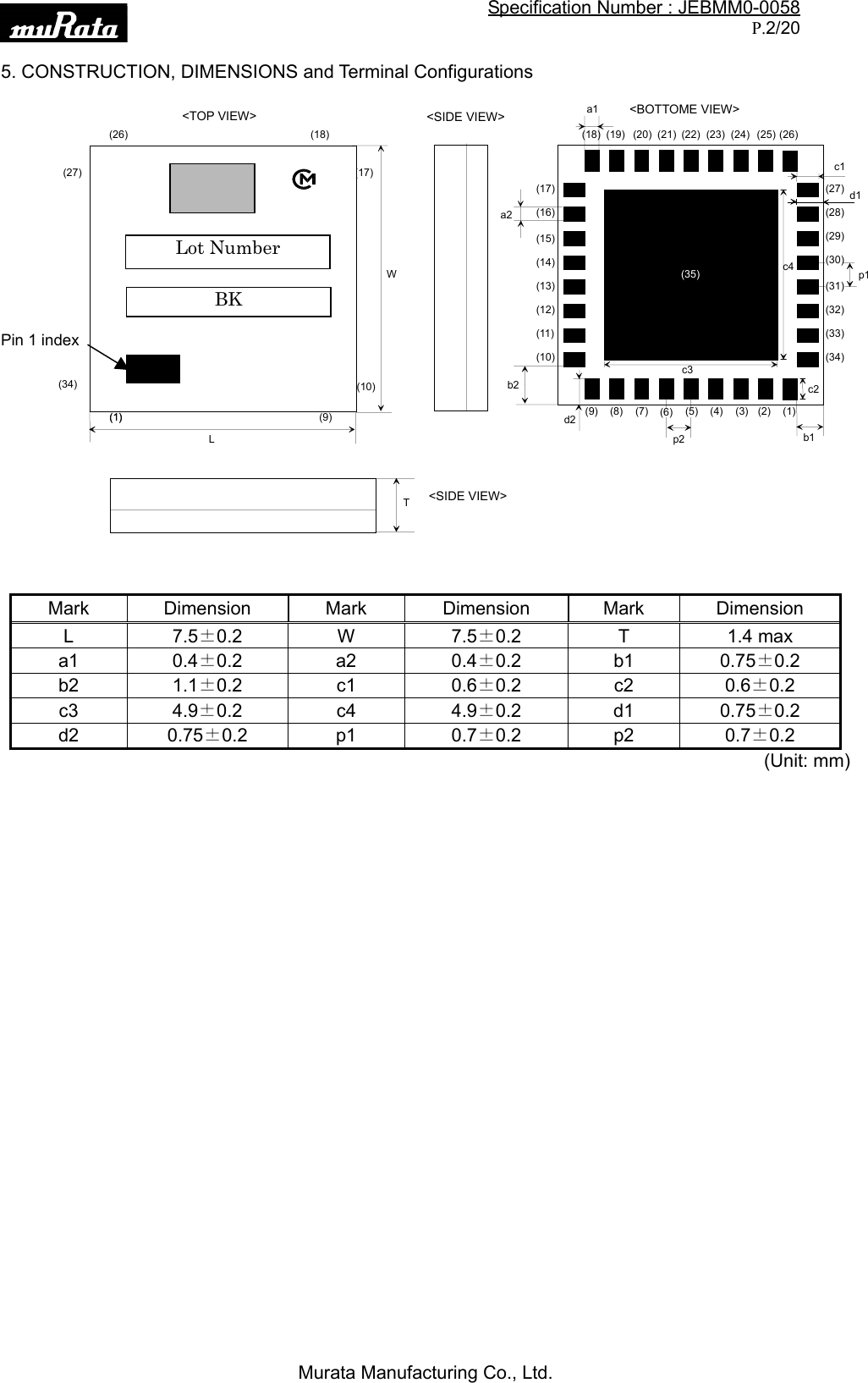
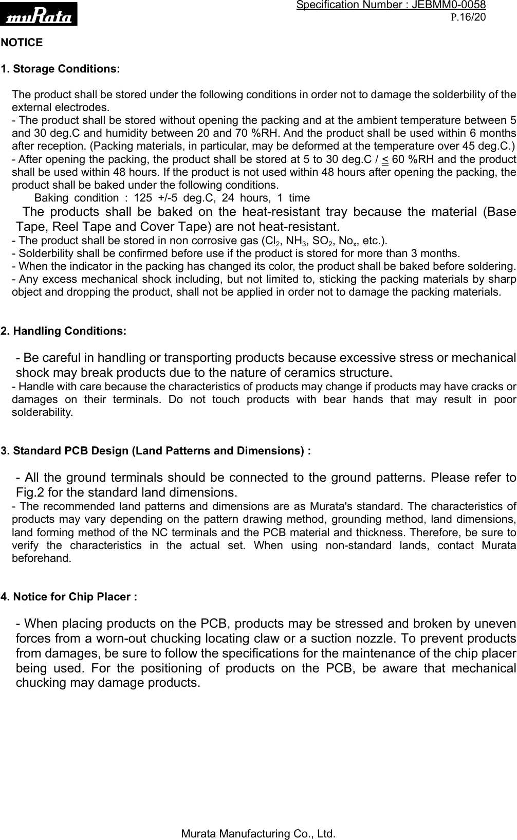
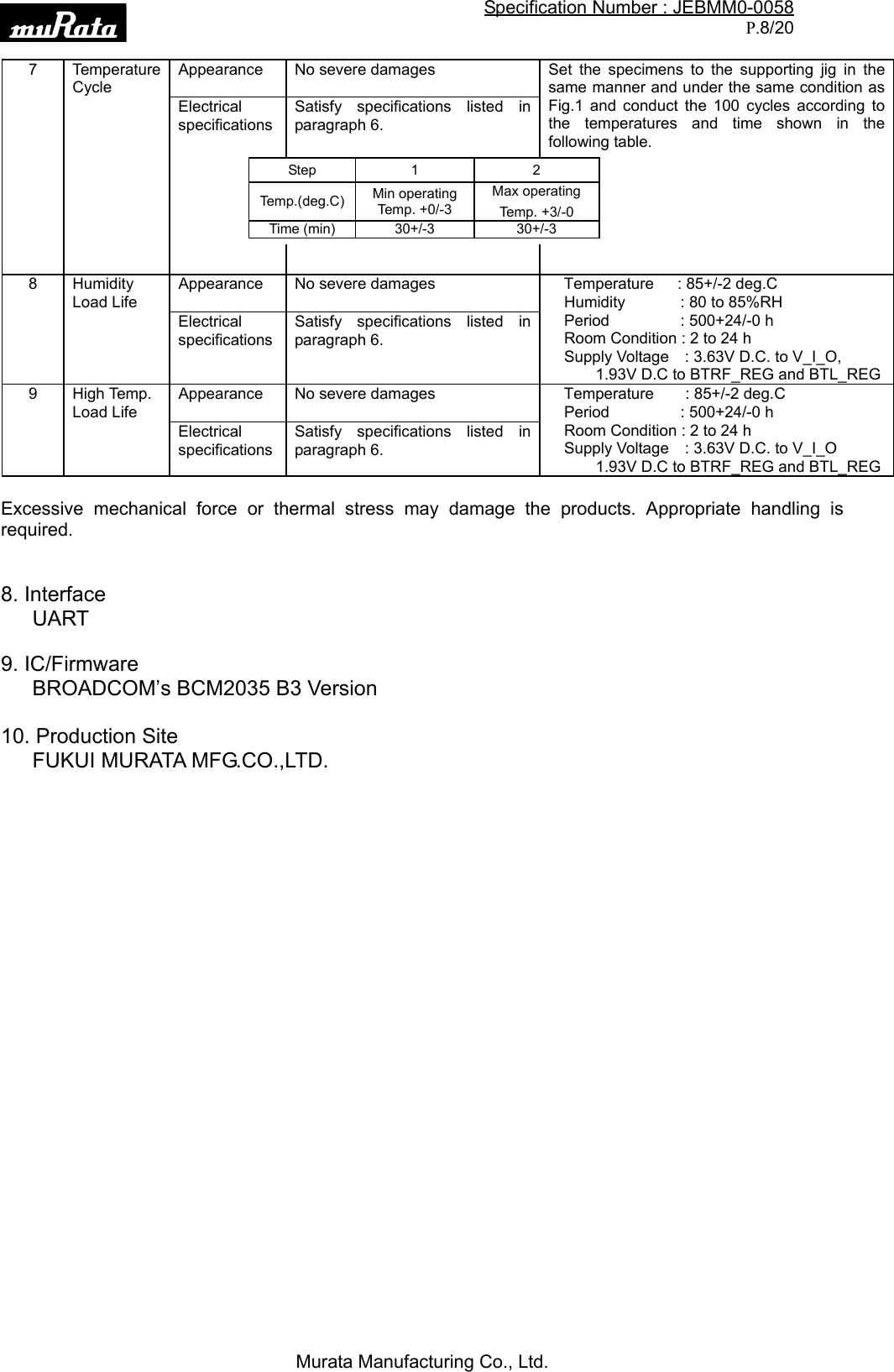
![Specification Number : JEBMM0-0058P.4/20Murata Manufacturing Co., Ltd.6. Electrical Characteristics6-1 Operating ConditionsMin Typ Max UnitOperating Temperature -20 +25 +70 deg.CSupply Voltage BTRF_REG, BTL_REG V_I_O1.711.711.82.81.983.63VV6-2-1 Characteristics +25degC,BTRF_REG/BTL_REG=1.8V, VIO=2.75VItems ContentsBluetooth specification Ver 1.2Channel spacing 1MHzNumber of RF channel 79Power class 2Operation mode(Rx/Tx) Time division multiplex either transmit or receiveFrequency hopping after one Rx/Tx cycleItems Min Typ Max Unit1.Current Consumption RF Register x57=xC6 1.1 BTRF_REG_IDC_max DH5; 100% slot utilization;50% Rx/Tx slot duty cycle75 mA1.3 V_I_O_REG_IDC_max DH5; 100% slot utilization;50% Rx/Tx slot duty cycle10 mA-TX characteristics- Min Typ Max Unit2.Output Power -4 4 dBm3.Frequency range(Rx/Tx)2400.5~2483.5MHz4.-20dB bandwidth 1MHz5.Adjacent Channel Power *1 5.1 [M-N]=2-21 dBm 5.2 [M-N]≧3-41 dBm6.Modulation characteristics 6.1 Modulation δf1avg 145 173 kHz 6.2 Modulation δf2max 125 kHz 6.3 Modulationδf2avg/δf1avg 0.857.Initial Carrier Frequency Tolerance -45 45 kHz8.Carrier Frequency Drift 8.1 1slot -25 25 kHz 8.2 3slot -40 40 kHz 8.3 5slot -40 40 kHz 8.4 Maximum drift rate -20 20 kHz/50μs9.Out-of-Band Spurious Emissions 9.1 30-1000MHz (Operation Mode) -36 dBm 9.2 1000-12750MHz (Operation Mode) -30 dBm 9.3 1800-1900MHz(Operation Mode) -47 dBm 9.4 2110-2170MHz (Operation Mode) -75 dBm 9.5 5150-5300MHz (Operation Mode) -47 dBm](https://usermanual.wiki/Acer-orporated/N300.Bluetooth-manual/User-Guide-600225-Page-5.png)
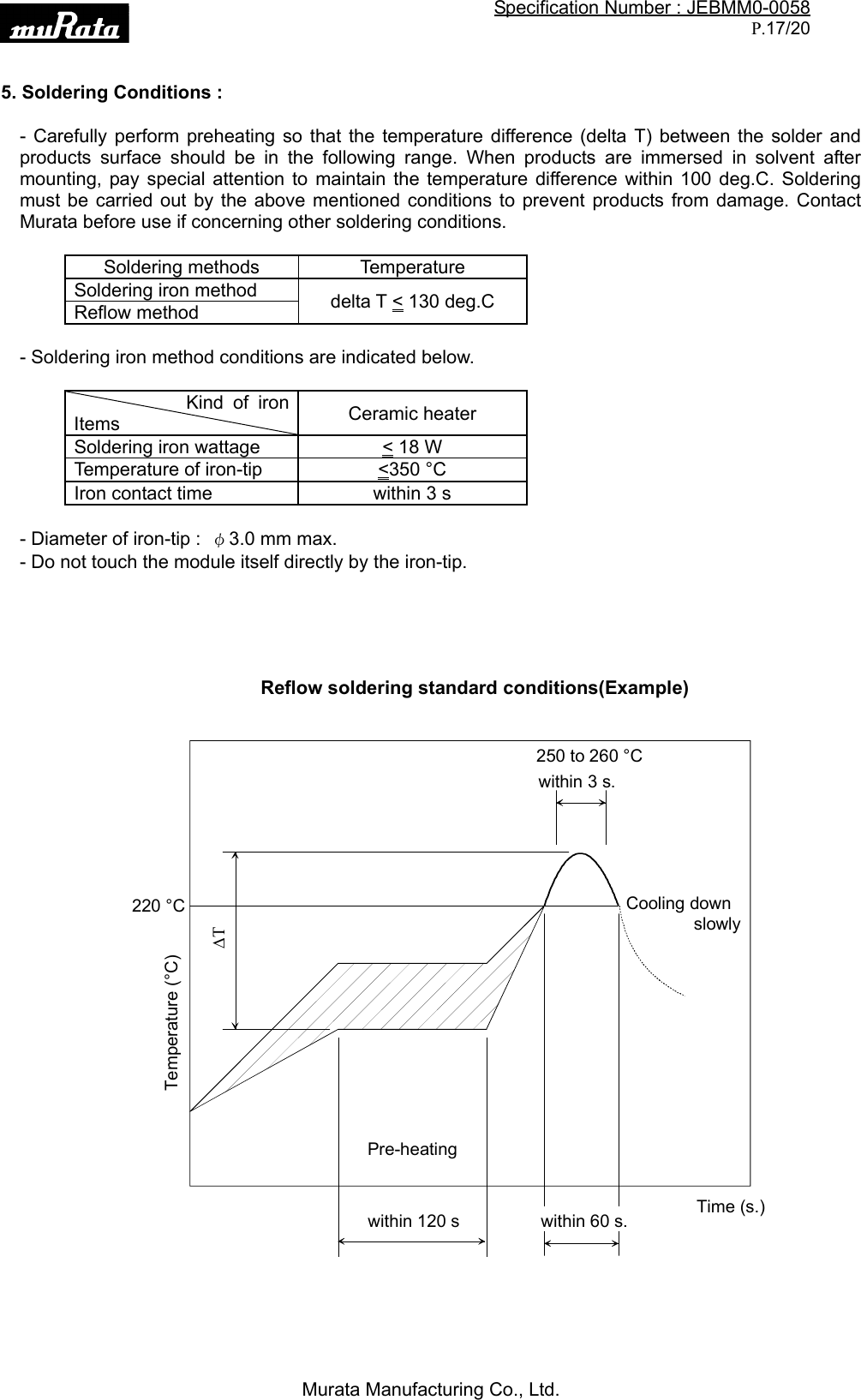
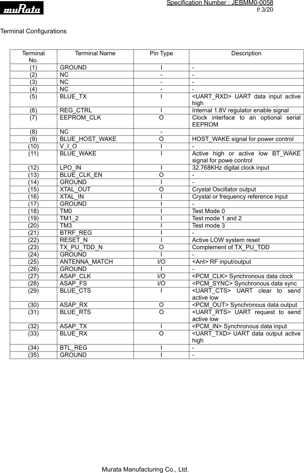
![Specification Number : JEBMM0-0058P.6/20Murata Manufacturing Co., Ltd.6-2-2. Extreme condition : -20 to +70degC, BTRF_REG/BTL_REG=1.71-1.98V, VIO=1.71-3.63VItems Min Typ Max Unit1.Current Consumption RF Register x57=xC6 1.1 BTRF_REG_IDC_max DH5; 100% slot utilization;50% Rx/Tx slot duty cycle80 mA1.3 V_I_O_REG_IDC_max DH5; 100% slot utilization;50% Rx/Tx slot duty cycle12 mA-TX characteristics- Min Typ Max Unit2.Output Power -6 +6 dBm3.Frequency range(Rx/Tx)2400.5~2483.5MHz4.-20dB bandwidth 1MHz5.Adjacent Channel Power *1 5.1 [M-N]=2-20 dBm 5.2 [M-N]≧3-40 dBm6.Modulation characteristics 6.1 Modulation δf1avg 145 175 kHz 6.2 Modulation δf2max 115 kHz 6.3 Modulationδf2avg/δf1avg 0.87.Initial Carrier Frequency Tolerance -75 75 kHz8.Carrier Frequency Drift 8.1 1slot -25 25 kHz 8.2 3slot -40 40 kHz 8.3 5slot -40 40 kHz 8.4 Maximum drift rate -20 20 kHz/50μs9.Out-of-Band Spurious Emissions 9.1 30-1000MHz (Operation Mode) -36 dBm 9.2 1000-12750MHz (Operation Mode) -30 dBm 9.3 1800-1900MHz(Operation Mode) -47 dBm 9.4 2110-2170MHz (Operation Mode) -65 dBm 9.5 5150-5300MHz (Operation Mode) -47 dBm-RX characteristics- min typ max unit10.Sensitivity (BER≦0.1%) 10.1 2402MHz -77 dBm 10.2 2441MHz -77 dBm 10.3 2480MHz -77 dBm*1 Up to three spurious responses within Bluetooth limits are allowed.NoteThe above mentioned values have been obtained according to our own measuring methods (testing jigFig.1) and may very depend on the circuit, in which the component is actually incorporated. Therefore,you are kindly requested to test the performance of the component actually in your set.](https://usermanual.wiki/Acer-orporated/N300.Bluetooth-manual/User-Guide-600225-Page-7.png)
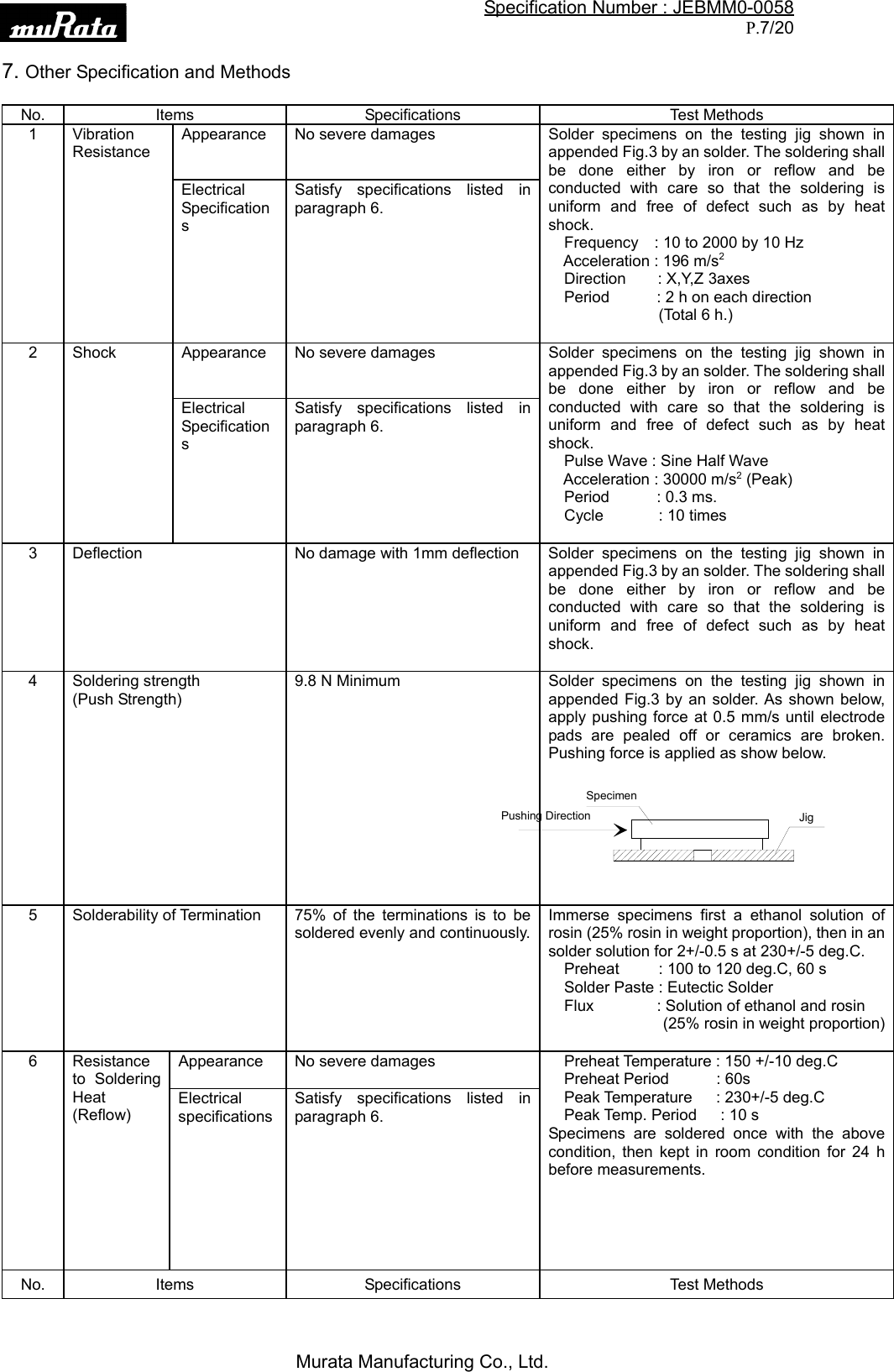
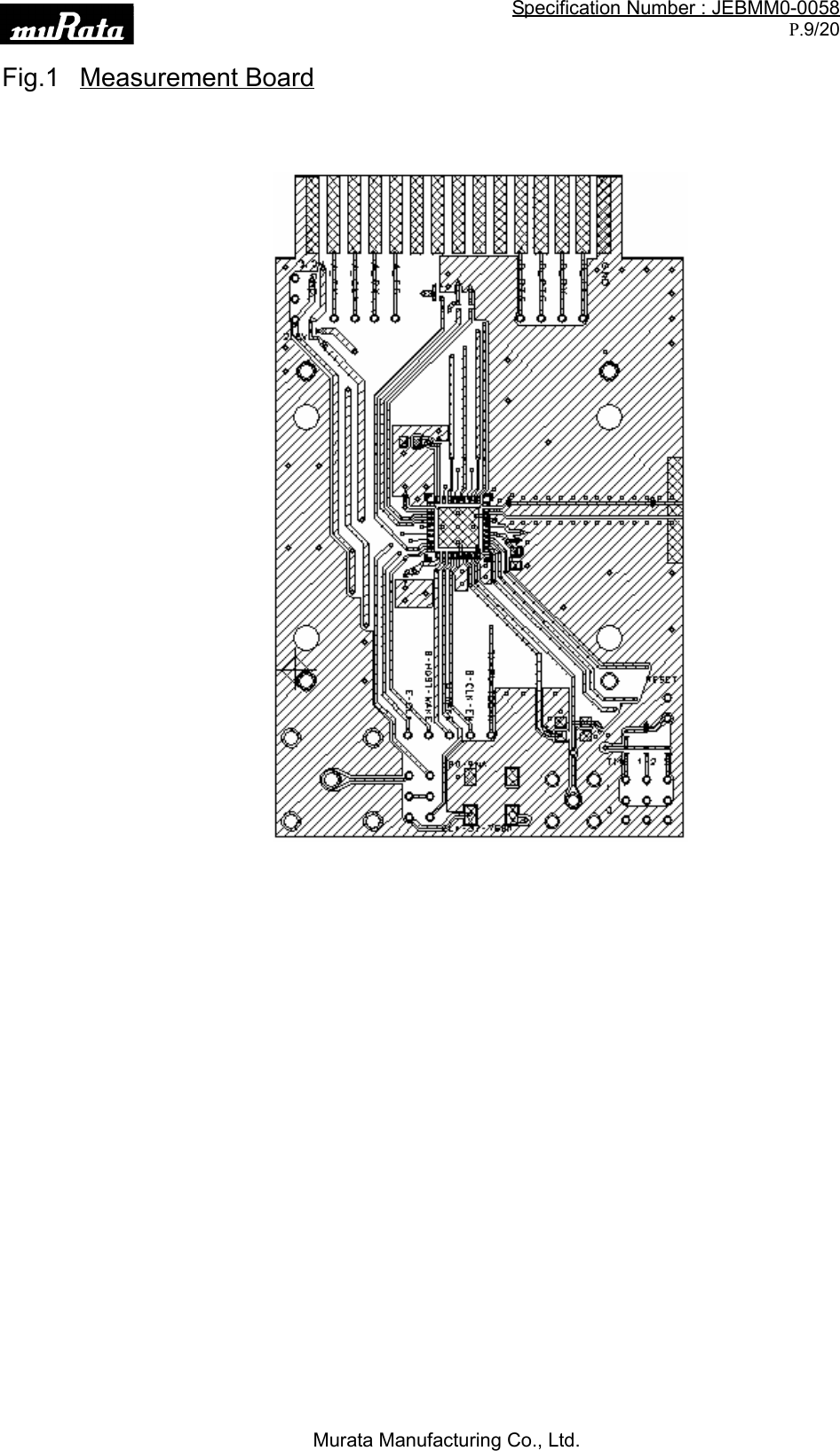
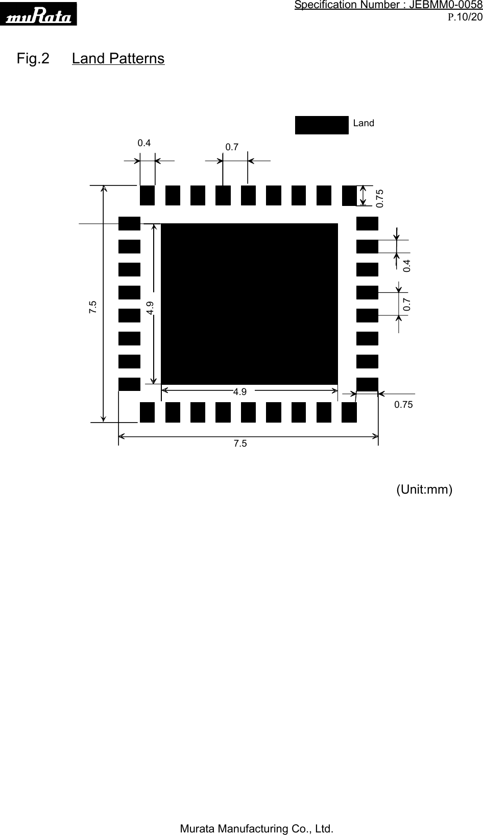
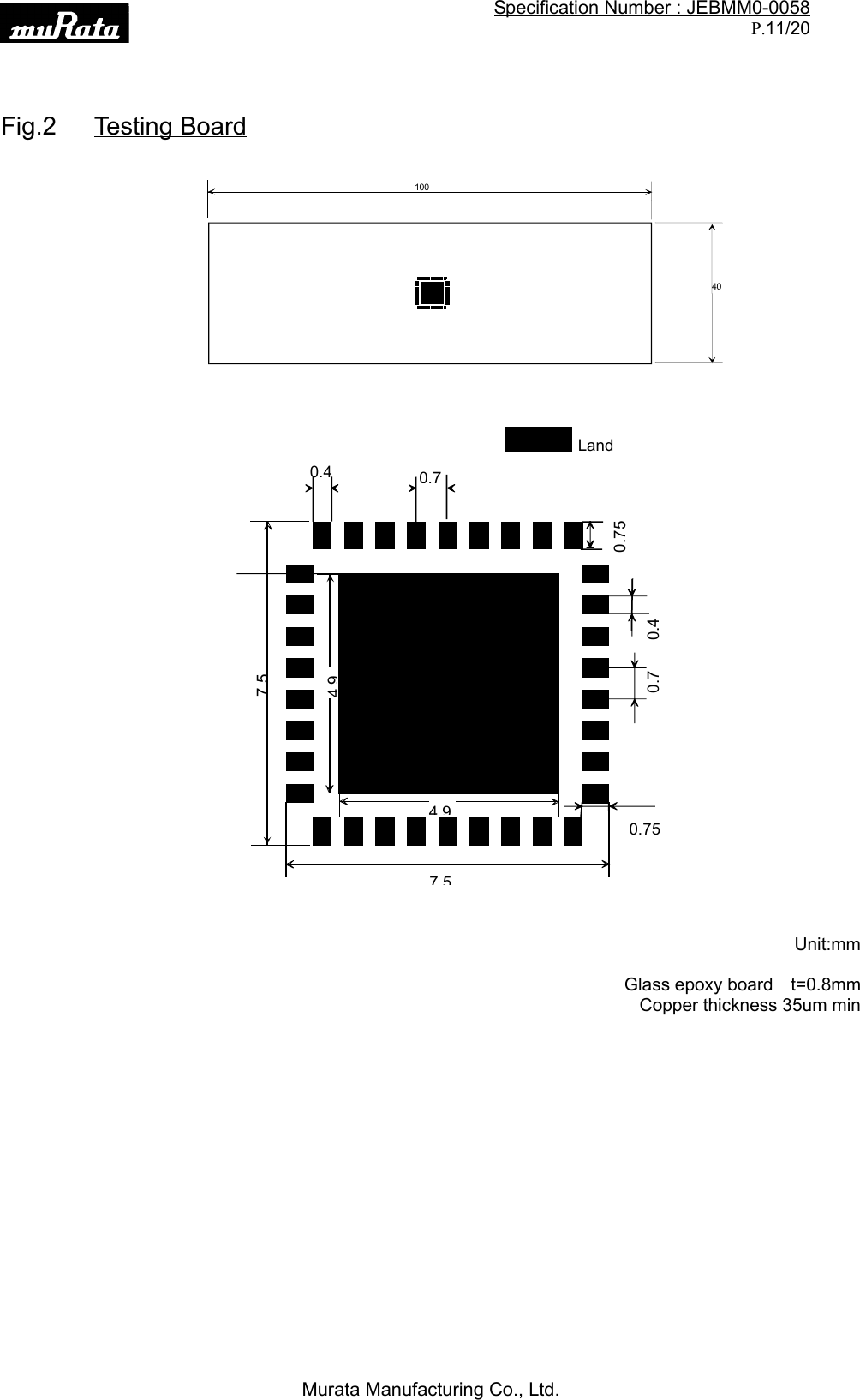
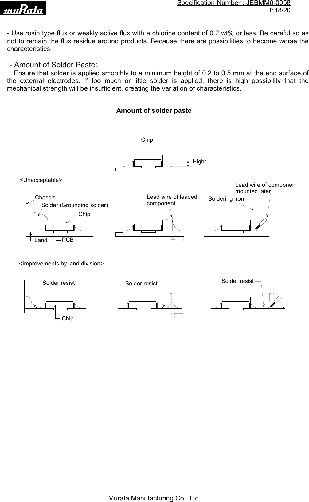
![Specification Number : JEBMM0-0058P.14/20Murata Manufacturing Co., Ltd.(3) Taping Diagrams[1] Feeding Hole : As specified in (1)[2] Hole for chip : As specified in (1)[3] Cover tape : 62 μm in thickness[4] Base tape : As specified in (1) 送り穴[2][3][4][3][1]送り穴ModuleFeeding DirectionFeeding Hole](https://usermanual.wiki/Acer-orporated/N300.Bluetooth-manual/User-Guide-600225-Page-15.png)