Acer orporated N300 PDA with WLAN and Bluetooth User Manual
Acer Incorporated PDA with WLAN and Bluetooth
UserManual.wiki
>
Acer orporated
>
N300 User Manual
>
WLAN manual
Contents
1.
Users Manual
2.
Bluetooth manual
3.
WLAN manual
WLAN manual
Navigation menu
Upload a User Manual
Namespaces
Wiki Guide
HTML
PDF
Info
Views
User Manual
Discussion / Help
Navigation
![Data Sheet Doc no: BB-WLAN2455-01 Version 0.4 Date: 05.25.2005 Page : 8 / 17 © Copyright Samsung Electro-Mechanics. All rights reserved. 2 Software specifications 2.1 OS Support & Driver 2.1.1 Available drivers [SWL-2455C] - Windows XP(Test purpose Only) - Windows CE.NET 4.2, 5.0 - Pocket PC 2003(SE) and higher - Linux [SWL-2455SD] - Windows CE.NET 5.0 - Pocket PC 2005 and higher - Linux - 2.2 Security - WEP - TKIP,AES - 802.1x - WPA - CCX - WPA2 2.3 Utility - RF TEST TOOL - WLAN status program 2.4 Other Feature - WME](https://usermanual.wiki/Acer-orporated/N300.WLAN-manual/User-Guide-600226-Page-8.png)
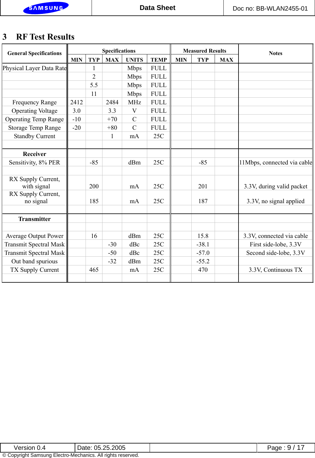
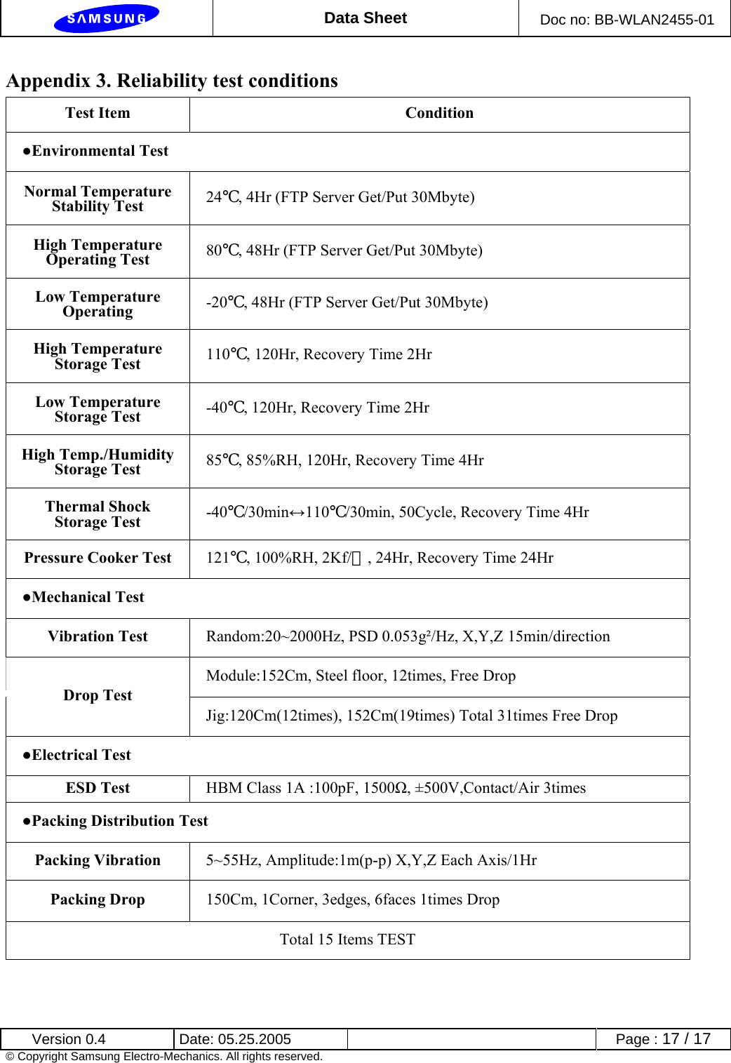
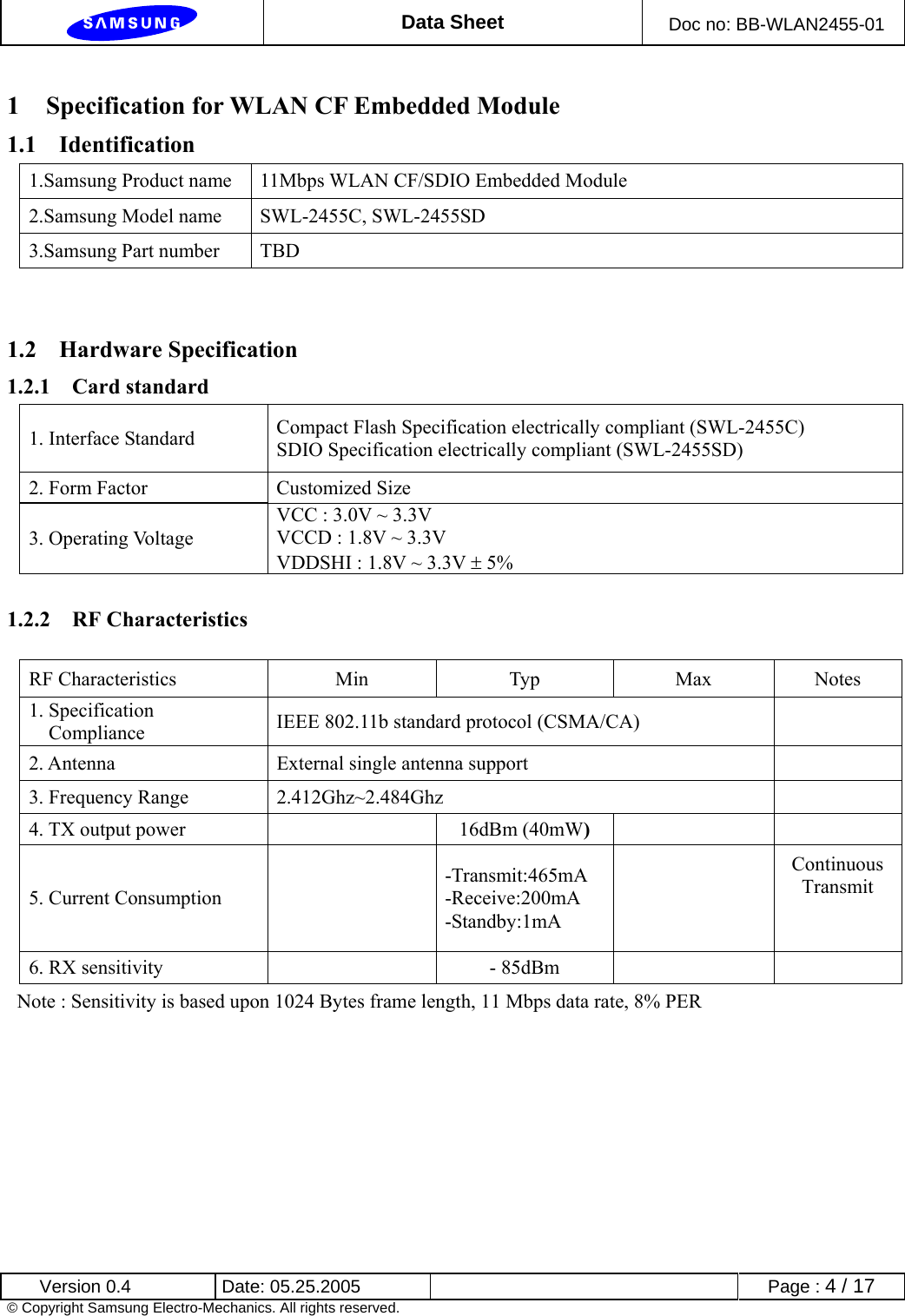
![Data Sheet Doc no: BB-WLAN2455-01 Version 0.4 Date: 05.25.2005 Page : 13 / 17 © Copyright Samsung Electro-Mechanics. All rights reserved. Appendix 1. Pin description. * I/O : Digital Input/Output, I : Digital Input, O : Digital Output, A : Analog, PU : Pull up No. Compact Flash SDIO Type Internal Resister Description 1 GND GND Ground Ground 2 D03 NC I/O 100K PU CF : Data line 3 3 D04 NC I/O 100K PU CF : Data line 4 4 D05 NC I/O 100K PU CF : Data line 5 5 D06 NC I/O 100K PU CF : Data line 6 6 D07 NC I/O 100K PU CF : Data line 7 7 CE1# NC I 100K PUCF Card Enable 1, This enables even-numbered address bytes. 8 MOD1 MOD1 I/O Host interface mode configuration 1 This pin is used as configuration to set parameters a following a reset. To set a configuration bit to 0, attach a 100Kohm resister from this pin to ground. No external circuitry is required to set a configuration bit to 1 After reset is completed, this pin is used for AGC output in module 9 OE# SD_CMD I 100K PUCF : Output Enable. It is used to read data from the Card in Memory mode and to read the CIS and configuration registers. SD 1-bit/4-bit mode : Command/Response 10 A09 SD_DAT[2] I 100K PUCF : Address line 9 SD 4-bit mode : Data line bit 2 or Read wait(optional) SD 1-bit mode : Read Wait(optional) SPI mode : Reserved 11 A08 NC I 100K PU CF : Address line 8 12 A07 NC I 100K PU CF : Address line 7 13 VCCD VCCD Power Digital core power 14 A06 NC I 100K PU CF : Address line 6 15 A05 NC I 100K PU CF : Address line 5 16 A04 NC I 100K PU CF : Address line 4 17 A03 NC I 100K PU CF : Address line 3 18 A02 NC I 100K PU CF : Address line 2 19 A01 NC I 100K PU CF : Address line 1 20 A00 NC I 100K PU CF : Address line 0 21 D00 NC I/O 100K PU CF : Data line 0 22 D01 NC I/O 100K PU CF : Data line 1 23 D02 NC I/O 100K PU CF : Data line 2 24 IOIS16# NC O 100K PUCF : I/O mode A low signal indicates that a 16bit or odd byte only operation can be performed at the addressed port 25 BT_PRIORITY BT_PRIORITY I Bluetooth Priority Asserted 1 during local BT RX and TX slots. 26 BT_STATE BT_STATE I Bluetooth State 0 = normal priority, Rx 1 = high priority, Tx](https://usermanual.wiki/Acer-orporated/N300.WLAN-manual/User-Guide-600226-Page-13.png)
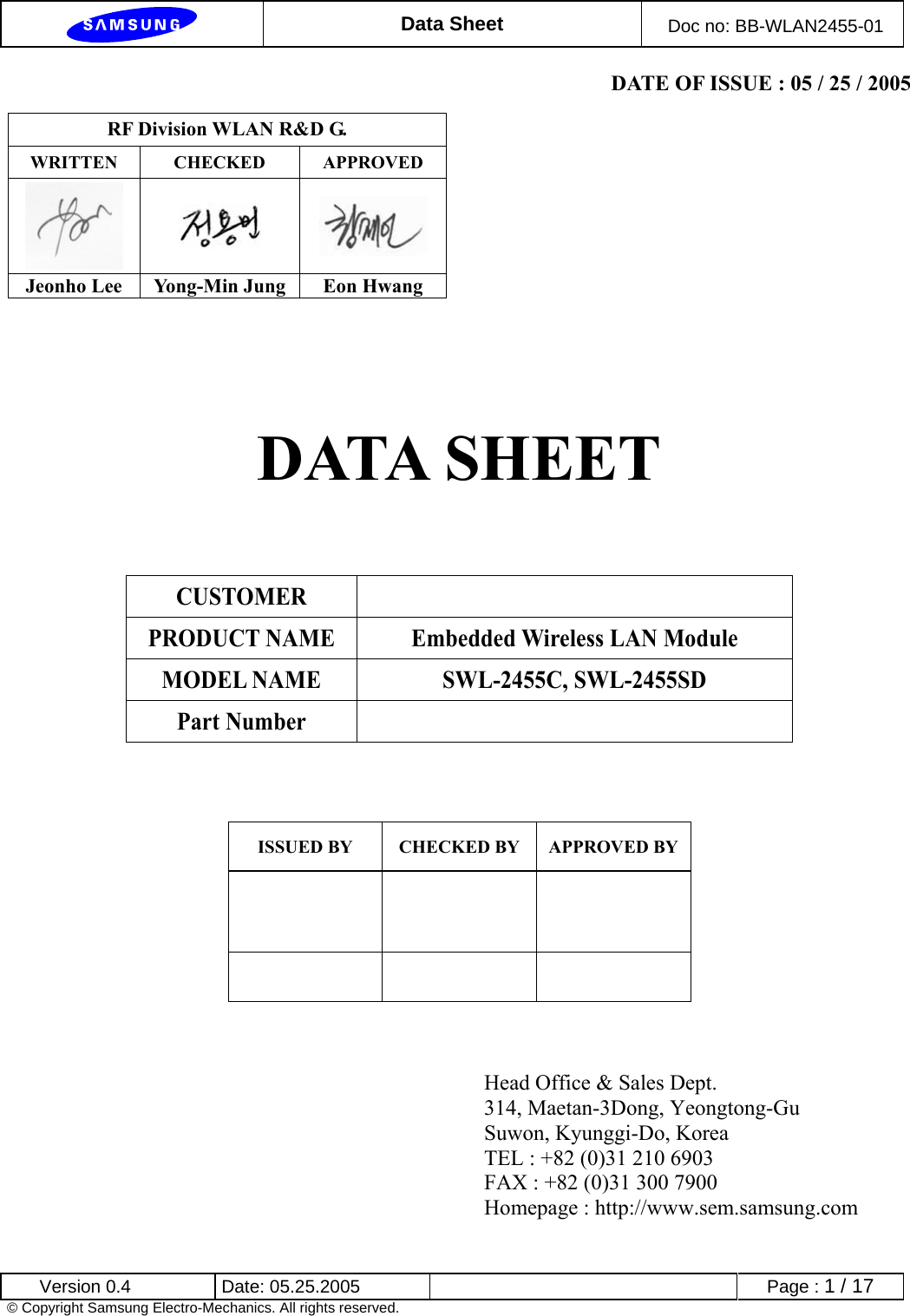
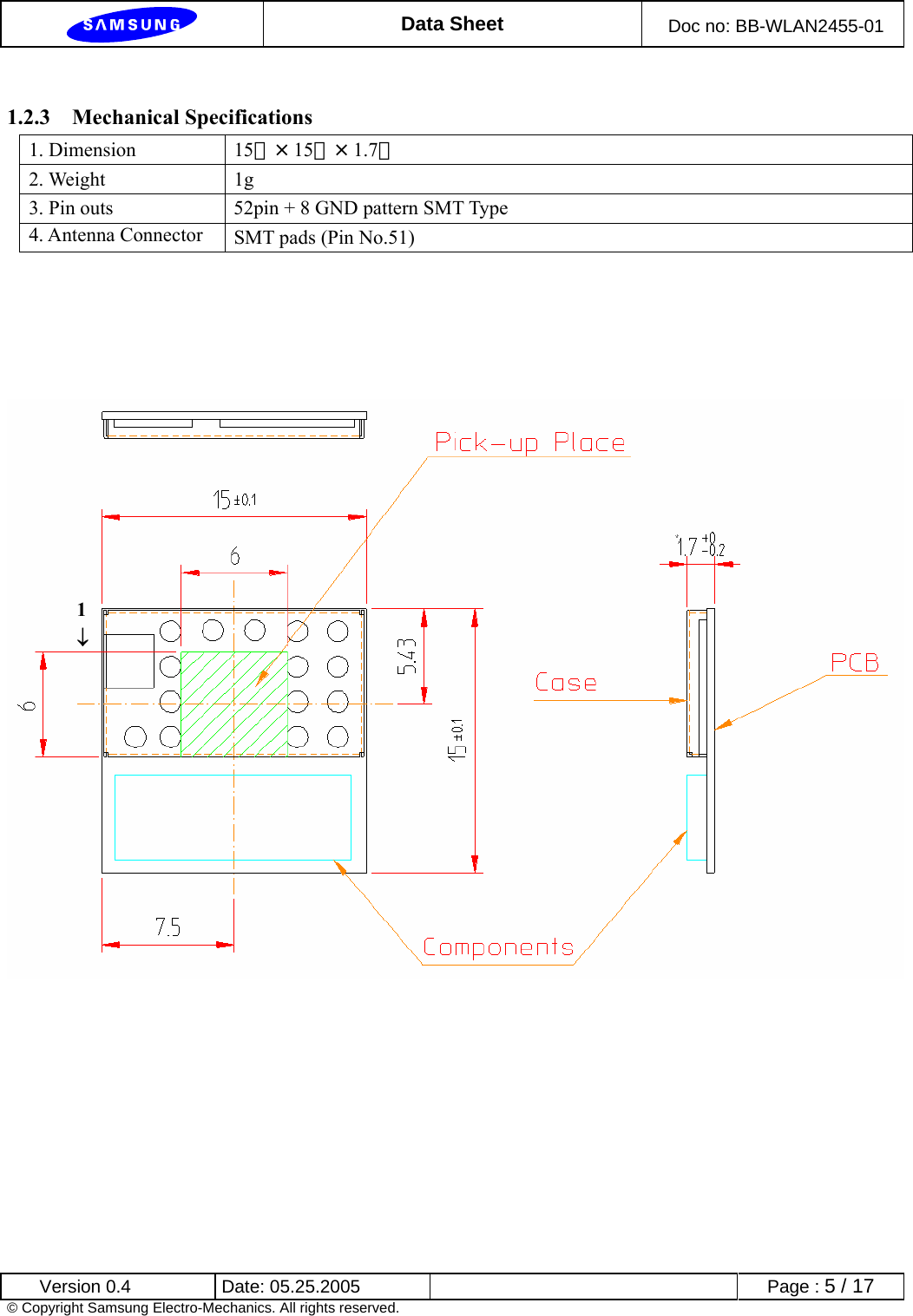
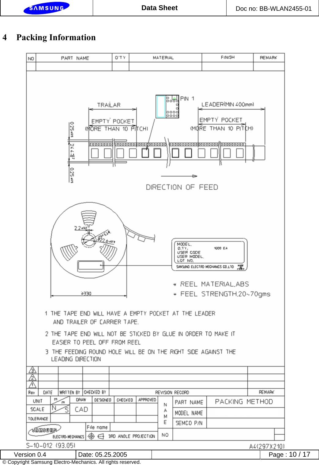
![Data Sheet Doc no: BB-WLAN2455-01 Version 0.4 Date: 05.25.2005 Page : 14 / 17 © Copyright Samsung Electro-Mechanics. All rights reserved. Priority is signaled after BT-PRIORITY has beed asserted. After priority signaling. BT_STATE indicates the Tx/Rx mode of BT radio 27 D11 NC I/O 100K PU CF Data line 11 28 D12 NC I/O 100K PU CF Data line 12 29 D13 NC I/O 100K PU CF Data line 13 30 D14 NC I/O 100K PU CF Data line 14 31 D15 NC I/O 100K PU CF Data line 15 32 CE2# SD_CLK, I 50K PU CF : Card Enable 2, This enables odd-numbered address bytes. SDIO 1-bit/4-bit mode : Clock SPI mode : Clock 33 WL_ACTIVE WL_ACTIVE O 50K PUWL_ACTIVE Transmission Confirmation to BT, active low signal. 0 = BT can transmit. Once asserted, it stays asserted until the BT device completes the transmission. Once allowed to transmit, BT device cannot stop in the middle of a packet. If asserted during BT transmission slot so that the Tx has not been started, the BT module shall not active the transmitter during the rest of the Tx period. Note : In WLAN Sleep mode, all I/O PADs are powered down. This PAD must stay at a low state even in power down mode. 34 IORD# SD_DAT[1] I 100K PUCF : I/O Read strobe SDIO 4-bit mode : Data line bit 1 SDIO 1-bit mode : Interrupt SPI mode : Reserved 35 IOWR# SD_DAT[3] I 50K PUCF : I/O Write strobe SDIO 4-bit mode : Data line bit 3 SDIO 1-bit mode : Reserved SPI mode : Card Select 36 WE# NC I 100K PU CF : Write enable 37 IREQ# NC O 100K PU CF : Interrupt Request 38 VCC VCC Power Power 39 PD# PD# I 200K PU Full power down 40 MOD2 MOD2 I/O Host interface mode configuration. This pin is used as configuration to set parameters a following a reset. To set a configuration bit to 0, attach a 100Kohm resister from this pin to ground. No external circuitry is required to set a configuration bit to 1 After reset is completed, this pin is used for AGC output in module 41 RESET RESET I 100K PU RESET, active high 42 WAIT# NC O 100K PUCF : Wait signal This is driven low by CF module to signal the host to delay completion of a momory or I/O cycle that is in progress 43 INPACK# NC O 100K PU CF : Input Acknowledge signal 44 REG# NC I 100K PUCF : REG This signal is used during Attribute memory accesses or I/O accesses. 45 LED_OUT# LED_OUT# I/O 200K PUGPIO for LED Blinking : AP scanning ON (Low): Link 46 VDDSHI VDDSHI Power This power supplies power to the IO cells.](https://usermanual.wiki/Acer-orporated/N300.WLAN-manual/User-Guide-600226-Page-14.png)
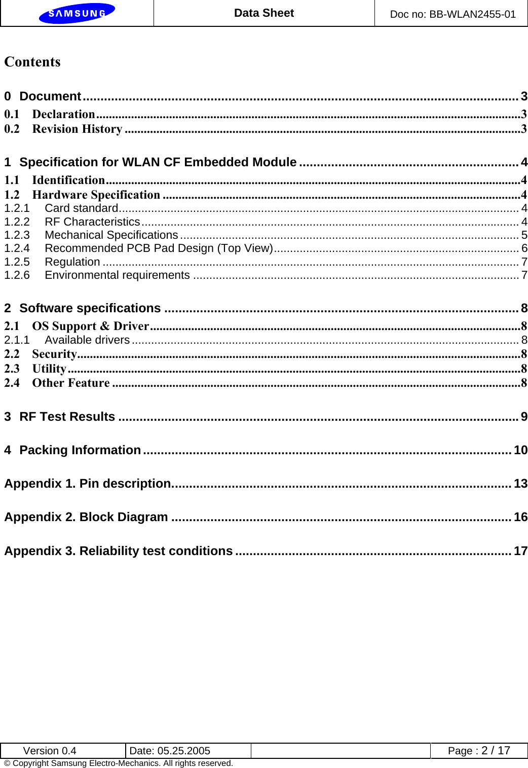
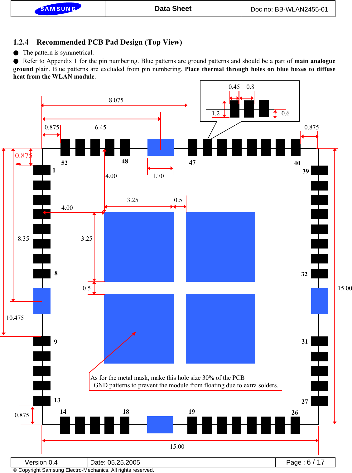
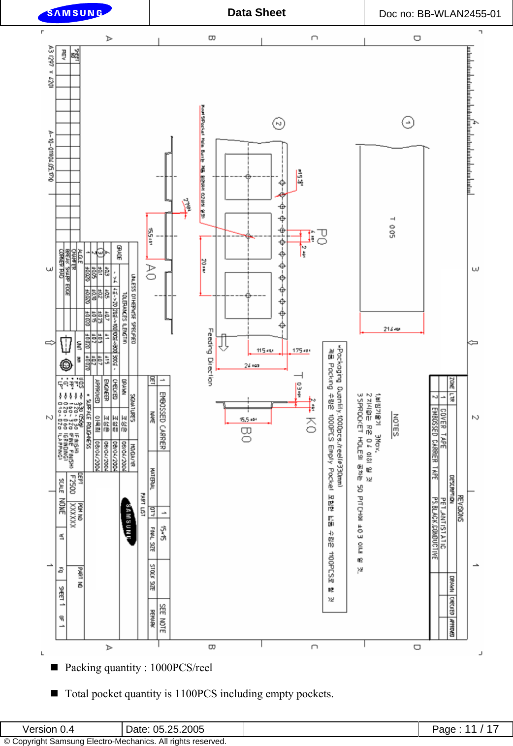
![Data Sheet Doc no: BB-WLAN2455-01 Version 0.4 Date: 05.25.2005 Page : 15 / 17 © Copyright Samsung Electro-Mechanics. All rights reserved. 47 D08 NC I/O 100K PU CF Data line 8 48 D09 NC I/O 100K PU CF Data line 9 49 D10 NC I/O 100K PU CF Data line 10 50 GND GND Ground Ground 51 RF_INOUT RF_INOUT A RF Input/Output 52 NC SD_DAT[0] I/O 100K PUSDIO 4-bit mode : Data line bit 0 SDIO 1-bit mode : Data line SPI mode : Data output * ‘#’ means that the signal is low active. * VCCD power voltage range is from 1.8V to 3.3V. Its current consumption has no relation with its voltage. It means that the lower the input voltage is the smaller power it consumes. It may be tied to the VCC, if you want to use the same voltage for both power inputs. * VDDSHI : Digital I/O Power Supply. When using CF interface, this pin must be connected to same supply as VCC. When using SDIO, this pin can be between 1.8 and 3.3V depending on the host interface I/O supply * PD# signal in CF interface is not matched with CF standard pin outs. This signal replaced the CSEL# signal in CF specification, and is used to set the full power down state. When this signal is connected to 0V, the module will be set to the full power down state. If you don’t use this function, just connect this pin to the main power. * LED_OUT# signal in CF interface is not matched with CF standard pin outs. This signal replaced the SPKR signal in CF specification, and is used to control the external LED. This signal is low active. * Pin No.25,26,33 are for the Bluetooth co-existence interface. If you connect these to the Bluetooth correctly, WLAN and Bluetooth will not conflict each other. * NC pins are used for test procedure or reserved for future use. These signal replaced the unused signals in CF specification. Just leave them unconnected. Connect CD1, CD2, VS1 from CF host to GND and leave VS2, SPKR, CSEL, STSCHG, A10 from CF host unconnected. * Host Interface mode configuration 2455 MOD1 MOD2 CF No connect Connect 100K ohm Pull down SDIO Connect 100K ohm Pull down No connect](https://usermanual.wiki/Acer-orporated/N300.WLAN-manual/User-Guide-600226-Page-15.png)