Acer orporated N300 PDA with WLAN and Bluetooth User Manual
Acer Incorporated PDA with WLAN and Bluetooth
Contents
- 1. Users Manual
- 2. Bluetooth manual
- 3. WLAN manual
WLAN manual
Data Sheet Doc no: BB-WLAN2455-01
Version 0.4 Date: 05.25.2005 Page : 1 / 17
© Copyright Samsung Electro-Mechanics. All rights reserved.
DATE OF ISSUE : 05 / 25 / 2005
DATA SHEET
RF Division WLAN R&D G.
WRITTEN CHECKED APPROVED
Jeonho Lee Yong-Min Jung Eon Hwang
CUSTOMER
PRODUCT NAME Embedded Wireless LAN Module
MODEL NAME SWL-2455C, SWL-2455SD
Part Number
ISSUED BY CHECKED BY APPROVED BY
Head Office & Sales Dept.
314, Maetan-3Dong, Yeongtong-Gu
Suwon, Kyunggi-Do, Korea
TEL : +82 (0)31 210 6903
FAX : +82 (0)31 300 7900
Homepage : http://www.sem.samsung.com

Data Sheet Doc no: BB-WLAN2455-01
Version 0.4 Date: 05.25.2005 Page : 2 / 17
© Copyright Samsung Electro-Mechanics. All rights reserved.
Contents
0 Document...........................................................................................................................3
0.1 Declaration......................................................................................................................................3
0.2 Revision History .............................................................................................................................3
1 Specification for WLAN CF Embedded Module ..............................................................4
1.1 Identification...................................................................................................................................4
1.2 Hardware Specification .................................................................................................................4
1.2.1 Card standard............................................................................................................................ 4
1.2.2 RF Characteristics..................................................................................................................... 4
1.2.3 Mechanical Specifications......................................................................................................... 5
1.2.4 Recommended PCB Pad Design (Top View)............................................................................ 6
1.2.5 Regulation ................................................................................................................................. 7
1.2.6 Environmental requirements .....................................................................................................7
2 Software specifications ....................................................................................................8
2.1 OS Support & Driver.....................................................................................................................8
2.1.1 Available drivers........................................................................................................................ 8
2.2 Security............................................................................................................................................8
2.3 Utility...............................................................................................................................................8
2.4 Other Feature .................................................................................................................................8
3 RF Test Results .................................................................................................................9
4 Packing Information........................................................................................................10
Appendix 1. Pin description................................................................................................ 13
Appendix 2. Block Diagram ................................................................................................16
Appendix 3. Reliability test conditions ..............................................................................17

Data Sheet Doc no: BB-WLAN2455-01
Version 0.4 Date: 05.25.2005 Page : 3 / 17
© Copyright Samsung Electro-Mechanics. All rights reserved.
0 Document
0.1 Declaration
This specification is intended for Samsung 11Mbps embedded wireless LAN module.
0.2 Revision History
08/12/2004 Created
03/24/2005 updated Operating Voltage Page 4
updated Recommended pad design Page 6
updated S/W Drivers Page 8
updated Pin Map Page10
04/20/2005 updated Interface Standard Page 4
updated Current consumption Page 4
updated Recommended pad design Page 6
updated Packing Information Page 10~12
updated Interface mode configuration Page 14
04/20/2005 updated Current consumption, RF test results Page 4,9
05/25/2005 updated Pin description and Reliability test conditions Page 13~17
Data Sheet Doc no: BB-WLAN2455-01
Version 0.4 Date: 05.25.2005 Page : 4 / 17
© Copyright Samsung Electro-Mechanics. All rights reserved.
1 Specification for WLAN CF Embedded Module
1.1 Identification
1.Samsung Product name 11Mbps WLAN CF/SDIO Embedded Module
2.Samsung Model name SWL-2455C, SWL-2455SD
3.Samsung Part number TBD
1.2 Hardware Specification
1.2.1 Card standard
1. Interface Standard Compact Flash Specification electrically compliant (SWL-2455C)
SDIO Specification electrically compliant (SWL-2455SD)
2. Form Factor Customized Size
3. Operating Voltage
VCC : 3.0V ~ 3.3V
VCCD : 1.8V ~ 3.3V
VDDSHI : 1.8V ~ 3.3V ± 5%
1.2.2 RF Characteristics
RF Characteristics Min Typ Max Notes
1. Specification
Compliance IEEE 802.11b standard protocol (CSMA/CA)
2. Antenna External single antenna support
3. Frequency Range 2.412Ghz~2.484Ghz
4. TX output power 16dBm (40mW)
5. Current Consumption
-Transmit:465mA
-Receive:200mA
-Standby:1mA
Continuous
Transmit
6. RX sensitivity - 85dBm
Note : Sensitivity is based upon 1024 Bytes frame length, 11 Mbps data rate, 8% PER
Data Sheet Doc no: BB-WLAN2455-01
Version 0.4 Date: 05.25.2005 Page : 5 / 17
© Copyright Samsung Electro-Mechanics. All rights reserved.
1.2.3 Mechanical Specifications
1. Dimension 15㎜×15㎜×1.7㎜
2. Weight 1g
3. Pin outs 52pin + 8 GND pattern SMT Type
4. Antenna Connector SMT pads (Pin No.51)
1
↓
Data Sheet Doc no: BB-WLAN2455-01
Version 0.4 Date: 05.25.2005 Page : 6 / 17
© Copyright Samsung Electro-Mechanics. All rights reserved.
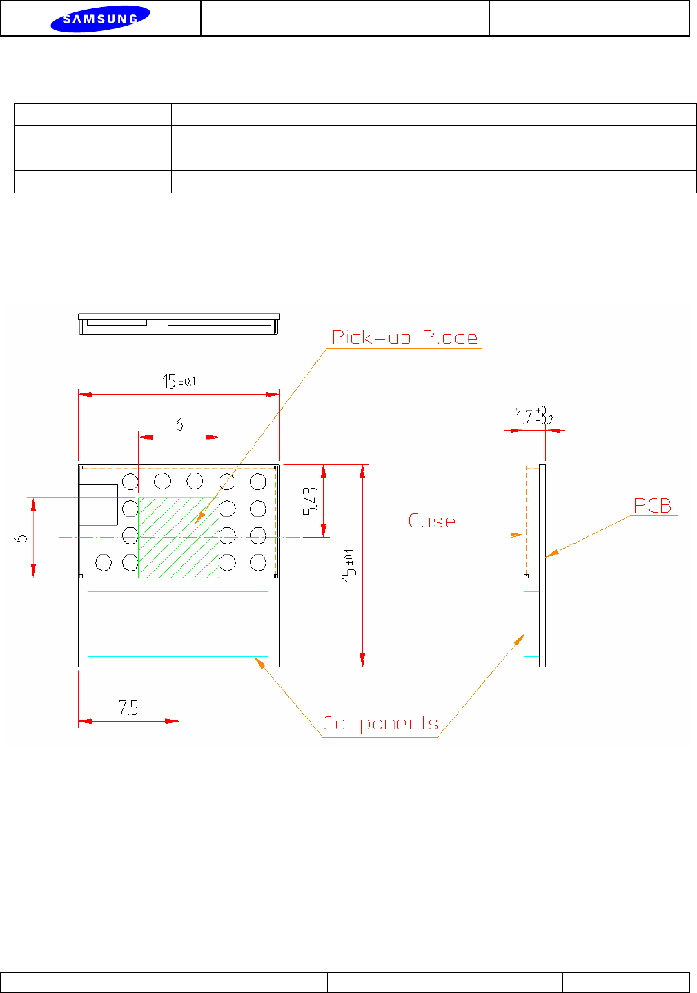
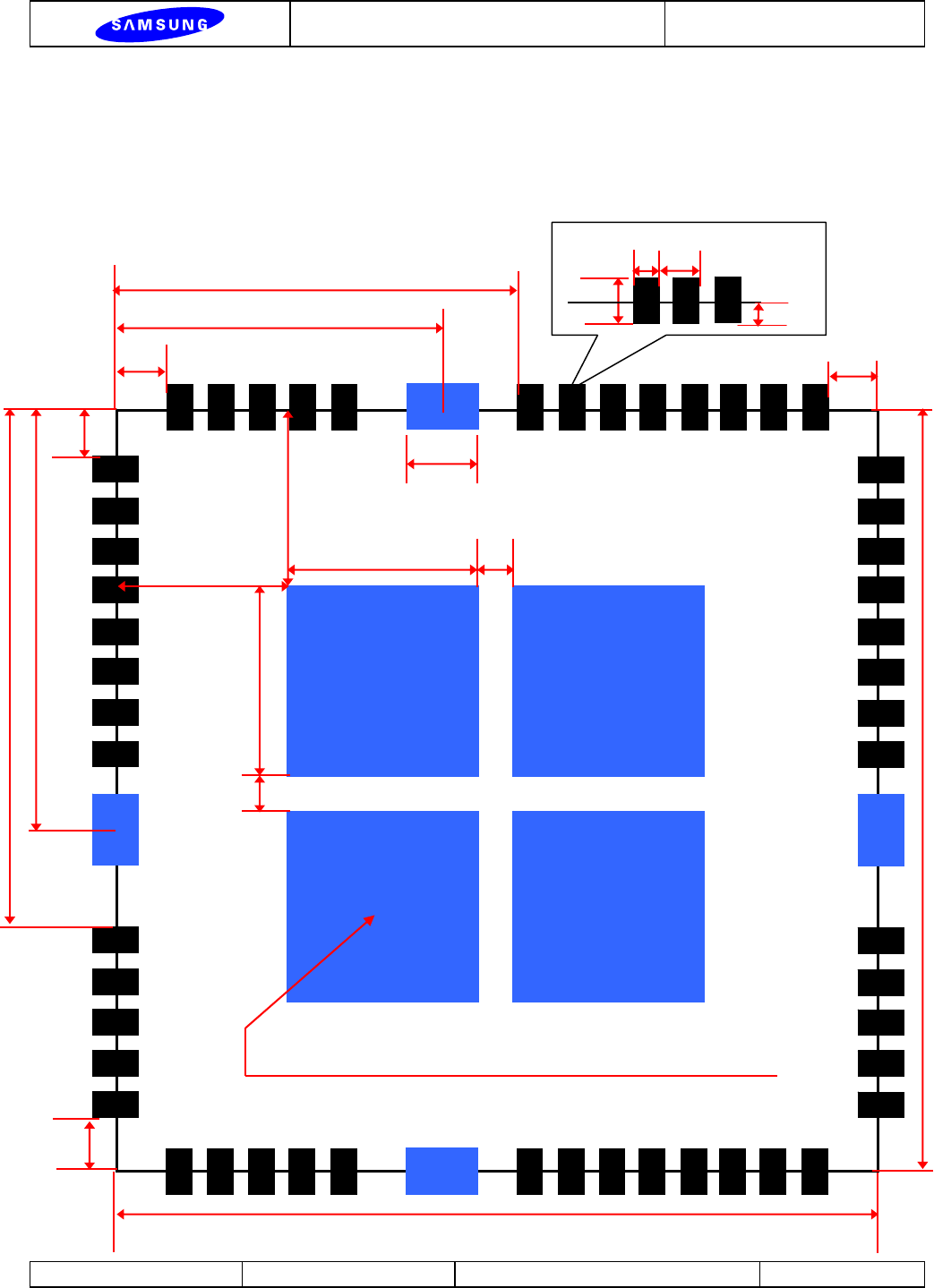
1.2.4 Recommended PCB Pad Design (Top View)
● The pattern is symmetrical.
● Refer to Appendix 1 for the pin numbering. Blue patterns are ground patterns and should be a part of main analogue
ground plain. Blue patterns are excluded from pin numbering. Place thermal through holes on blue boxes to diffuse
heat from the WLAN module.
0.875
●
8.35 3.25
0.875 6.45 0.875
8.075
10.475
As for the metal mask, make this hole size 30% of the PCB
GND patterns to prevent the module from floating due to extra solders.
0.875
15.00
3.25 0.5
4.00
0.45 0.8
1.2 0.6
4.00 1.70
0.5 15.00
1
8
9
13
14
18
19
26
27
31
32
39
40
47
52
48

Data Sheet Doc no: BB-WLAN2455-01
Version 0.4 Date: 05.25.2005 Page : 7 / 17
© Copyright Samsung Electro-Mechanics. All rights reserved.
1.2.5 Regulation
1. Europe Not yet submitted
2. USA,Canada Not yet submitted
3. Others Not yet submitted
1.2.6 Environmental requirements
1. Operating Temperature -10°C ~ +70°C
2. Storage Temperature -20°C ~ +80°C
3. Operating Humidity 0% ~ 90%(RH)

Data Sheet Doc no: BB-WLAN2455-01
Version 0.4 Date: 05.25.2005 Page : 8 / 17
© Copyright Samsung Electro-Mechanics. All rights reserved.
2 Software specifications
2.1 OS Support & Driver
2.1.1 Available drivers
[SWL-2455C]
- Windows XP(Test purpose Only)
- Windows CE.NET 4.2, 5.0
- Pocket PC 2003(SE) and higher
- Linux
[SWL-2455SD]
- Windows CE.NET 5.0
- Pocket PC 2005 and higher
- Linux
-
2.2 Security
- WEP
- TKIP,AES
- 802.1x
- WPA
- CCX
- WPA2
2.3 Utility
- RF TEST TOOL
- WLAN status program
2.4 Other Feature
- WME

Data Sheet Doc no: BB-WLAN2455-01
Version 0.4 Date: 05.25.2005 Page : 9 / 17
© Copyright Samsung Electro-Mechanics. All rights reserved.
3 RF Test Results
Specifications Measured Results
General Specifications
MIN TYP MAX UNITS TEMP MIN TYP MAX
Notes
Physical Layer Data Rate 1 Mbps FULL
2 Mbps FULL
5.5 Mbps FULL
11 Mbps FULL
Frequency Range 2412 2484 MHz FULL
Operating Voltage 3.0 3.3 V FULL
Operating Temp Range -10 +70 C FULL
Storage Temp Range -20 +80 C FULL
Standby Current 1 mA 25C
Receiver
Sensitivity, 8% PER -85 dBm 25C -85 11Mbps, connected via cable
RX Supply Current,
with signal 200 mA 25C 201 3.3V, during valid packet
RX Supply Current,
no signal 185 mA 25C 187 3.3V, no signal applied
Transmitter
Average Output Power 16 dBm 25C 15.8 3.3V, connected via cable
Transmit Spectral Mask -30 dBc 25C -38.1 First side-lobe, 3.3V
Transmit Spectral Mask -50 dBc 25C -57.0 Second side-lobe, 3.3V
Out band spurious -32 dBm 25C -55.2
TX Supply Current 465 mA 25C 470 3.3V, Continuous TX
Data Sheet Doc no: BB-WLAN2455-01
Version 0.4 Date: 05.25.2005 Page : 10 / 17
© Copyright Samsung Electro-Mechanics. All rights reserved.
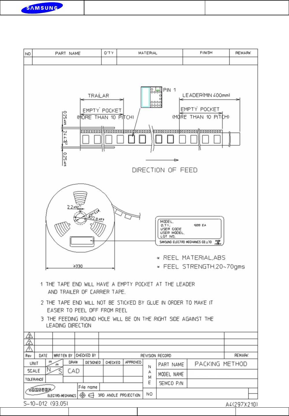
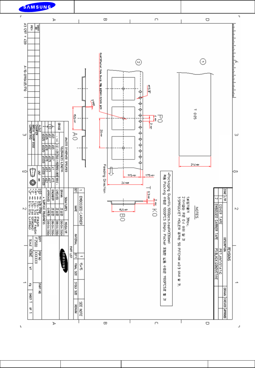
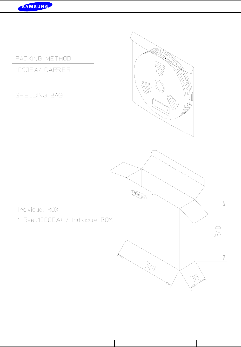
4 Packing Information
Data Sheet Doc no: BB-WLAN2455-01
Version 0.4 Date: 05.25.2005 Page : 11 / 17
© Copyright Samsung Electro-Mechanics. All rights reserved.
Packing quantity : 1000PCS/reel
Total pocket quantity is 1100PCS including empty pockets.
Data Sheet Doc no: BB-WLAN2455-01
Version 0.4 Date: 05.25.2005 Page : 12 / 17
© Copyright Samsung Electro-Mechanics. All rights reserved.
Max storage condition : -40℃ ~ 80℃
※ Recommended to be kept in room temperature.
Data Sheet Doc no: BB-WLAN2455-01
Version 0.4 Date: 05.25.2005 Page : 13 / 17
© Copyright Samsung Electro-Mechanics. All rights reserved.
Appendix 1. Pin description.
* I/O : Digital Input/Output, I : Digital Input, O : Digital Output, A : Analog, PU : Pull up
No. Compact Flash SDIO Type Internal
Resister Description
1 GND GND Ground Ground
2 D03 NC I/O 100K PU CF : Data line 3
3 D04 NC I/O 100K PU CF : Data line 4
4 D05 NC I/O 100K PU CF : Data line 5
5 D06 NC I/O 100K PU CF : Data line 6
6 D07 NC I/O 100K PU CF : Data line 7
7 CE1# NC I 100K PU
CF Card Enable 1,
This enables even-numbered address bytes.
8 MOD1 MOD1 I/O
Host interface mode configuration 1
This pin is used as configuration to set parameters a
following a reset. To set a configuration bit to 0, attach a
100Kohm resister from this pin to ground. No external
circuitry is required to set a configuration bit to 1
After reset is completed, this pin is used for AGC output
in module
9 OE# SD_CMD I 100K PU
CF : Output Enable. It is used to read data from the Card
in Memory mode and to read the CIS and configuration
registers.
SD 1-bit/4-bit mode : Command/Response
10 A09 SD_DAT[2] I 100K PU
CF : Address line 9
SD 4-bit mode : Data line bit 2 or Read wait(optional)
SD 1-bit mode : Read Wait(optional)
SPI mode : Reserved
11 A08 NC I 100K PU CF : Address line 8
12 A07 NC I 100K PU CF : Address line 7
13 VCCD VCCD Power Digital core power
14 A06 NC I 100K PU CF : Address line 6
15 A05 NC I 100K PU CF : Address line 5
16 A04 NC I 100K PU CF : Address line 4
17 A03 NC I 100K PU CF : Address line 3
18 A02 NC I 100K PU CF : Address line 2
19 A01 NC I 100K PU CF : Address line 1
20 A00 NC I 100K PU CF : Address line 0
21 D00 NC I/O 100K PU CF : Data line 0
22 D01 NC I/O 100K PU CF : Data line 1
23 D02 NC I/O 100K PU CF : Data line 2
24 IOIS16# NC O 100K PU
CF : I/O mode
A low signal indicates that a 16bit or odd byte only
operation can be performed at the addressed port
25 BT_PRIORITY BT_PRIORITY I
Bluetooth Priority
Asserted 1 during local BT RX and TX slots.
26 BT_STATE BT_STATE I
Bluetooth State
0 = normal priority, Rx
1 = high priority, Tx
Data Sheet Doc no: BB-WLAN2455-01
Version 0.4 Date: 05.25.2005 Page : 14 / 17
© Copyright Samsung Electro-Mechanics. All rights reserved.
Priority is signaled after BT-PRIORITY has beed
asserted. After priority signaling. BT_STATE indicates
the Tx/Rx mode of BT radio
27 D11 NC I/O 100K PU CF Data line 11
28 D12 NC I/O 100K PU CF Data line 12
29 D13 NC I/O 100K PU CF Data line 13
30 D14 NC I/O 100K PU CF Data line 14
31 D15 NC I/O 100K PU CF Data line 15
32 CE2# SD_CLK, I 50K PU
CF : Card Enable 2,
This enables odd-numbered address bytes.
SDIO 1-bit/4-bit mode : Clock
SPI mode : Clock
33 WL_ACTIVE WL_ACTIVE O 50K PU
WL_ACTIVE
Transmission Confirmation to BT, active low signal. 0
= BT can transmit. Once asserted, it stays asserted until
the BT device completes the transmission. Once allowed
to transmit, BT device cannot stop in the middle of a
packet. If asserted during BT transmission slot so that the
Tx has not been started, the BT module shall not active
the transmitter during the rest of the Tx period.
Note : In WLAN Sleep mode, all I/O PADs are powered
down. This PAD must stay at a low state even in power
down mode.
34 IORD# SD_DAT[1] I 100K PU
CF : I/O Read strobe
SDIO 4-bit mode : Data line bit 1
SDIO 1-bit mode : Interrupt
SPI mode : Reserved
35 IOWR# SD_DAT[3] I 50K PU
CF : I/O Write strobe
SDIO 4-bit mode : Data line bit 3
SDIO 1-bit mode : Reserved
SPI mode : Card Select
36 WE# NC I 100K PU CF : Write enable
37 IREQ# NC O 100K PU CF : Interrupt Request
38 VCC VCC Power Power
39 PD# PD# I 200K PU Full power down
40 MOD2 MOD2 I/O
Host interface mode configuration.
This pin is used as configuration to set parameters a
following a reset. To set a configuration bit to 0, attach a
100Kohm resister from this pin to ground. No external
circuitry is required to set a configuration bit to 1
After reset is completed, this pin is used for AGC output
in module
41 RESET RESET I 100K PU RESET, active high
42 WAIT# NC O 100K PU
CF : Wait signal
This is driven low by CF module to signal the host to
delay completion of a momory or I/O cycle that is in
progress
43 INPACK# NC O 100K PU CF : Input Acknowledge signal
44 REG# NC I 100K PU
CF : REG
This signal is used during Attribute memory accesses or
I/O accesses.
45 LED_OUT# LED_OUT# I/O 200K PU
GPIO for LED
Blinking : AP scanning
ON (Low): Link
46 VDDSHI VDDSHI Power This power supplies power to the IO cells.
Data Sheet Doc no: BB-WLAN2455-01
Version 0.4 Date: 05.25.2005 Page : 15 / 17
© Copyright Samsung Electro-Mechanics. All rights reserved.
47 D08 NC I/O 100K PU CF Data line 8
48 D09 NC I/O 100K PU CF Data line 9
49 D10 NC I/O 100K PU CF Data line 10
50 GND GND Ground Ground
51 RF_INOUT RF_INOUT A RF Input/Output
52 NC SD_DAT[0] I/O 100K PU
SDIO 4-bit mode : Data line bit 0
SDIO 1-bit mode : Data line
SPI mode : Data output
* ‘#’ means that the signal is low active.
* VCCD power voltage range is from 1.8V to 3.3V. Its current consumption has no relation with its voltage. It
means that the lower the input voltage is the smaller power it consumes. It may be tied to the VCC, if you want
to use the same voltage for both power inputs.
* VDDSHI : Digital I/O Power Supply. When using CF interface, this pin must be connected to same supply as
VCC. When using SDIO, this pin can be between 1.8 and 3.3V depending on the host interface I/O supply
* PD# signal in CF interface is not matched with CF standard pin outs. This signal replaced the CSEL# signal in
CF specification, and is used to set the full power down state. When this signal is connected to 0V, the module
will be set to the full power down state. If you don’t use this function, just connect this pin to the main power.
* LED_OUT# signal in CF interface is not matched with CF standard pin outs. This signal replaced the SPKR
signal in CF specification, and is used to control the external LED. This signal is low active.
* Pin No.25,26,33 are for the Bluetooth co-existence interface. If you connect these to the Bluetooth correctly,
WLAN and Bluetooth will not conflict each other.
* NC pins are used for test procedure or reserved for future use. These signal replaced the unused signals in CF
specification. Just leave them unconnected. Connect CD1, CD2, VS1 from CF host to GND and leave VS2,
SPKR, CSEL, STSCHG, A10 from CF host unconnected.
* Host Interface mode configuration
2455 MOD1 MOD2
CF No connect Connect 100K ohm Pull down
SDIO Connect 100K ohm Pull down No connect
Data Sheet Doc no: BB-WLAN2455-01
Version 0.4 Date: 05.25.2005 Page : 16 / 17
© Copyright Samsung Electro-Mechanics. All rights reserved.
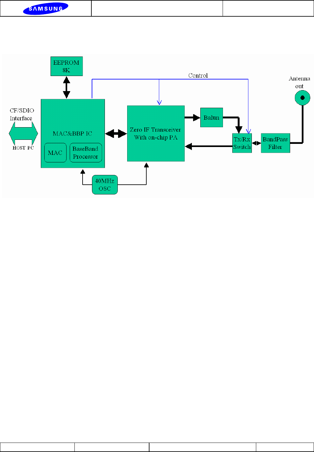
Appendix 2. Block Diagram

Data Sheet Doc no: BB-WLAN2455-01
Version 0.4 Date: 05.25.2005 Page : 17 / 17
© Copyright Samsung Electro-Mechanics. All rights reserved.
Appendix 3. Reliability test conditions
Test Item Condition
●Environmental Test
Normal Temperature
Stability Test 24℃, 4Hr (FTP Server Get/Put 30Mbyte)
High Temperature
Operating Test 80℃, 48Hr (FTP Server Get/Put 30Mbyte)
Low Temperature
Operating -20℃, 48Hr (FTP Server Get/Put 30Mbyte)
High Temperature
Storage Test 110℃, 120Hr, Recovery Time 2Hr
Low Temperature
Storage Test -40℃, 120Hr, Recovery Time 2Hr
High Temp./Humidity
Storage Test 85℃, 85%RH, 120Hr, Recovery Time 4Hr
Thermal Shock
Storage Test -40℃/30min↔110℃/30min, 50Cycle, Recovery Time 4Hr
Pressure Cooker Test 121℃, 100%RH, 2Kf/㎠, 24Hr, Recovery Time 24Hr
●Mechanical Test
Vibration Test Random:20~2000Hz, PSD 0.053g²/Hz, X,Y,Z 15min/direction
Module:152Cm, Steel floor, 12times, Free Drop
Drop Test
Jig:120Cm(12times), 152Cm(19times) Total 31times Free Drop
●Electrical Test
ESD Test HBM Class 1A :100pF, 1500Ω, ±500V,Contact/Air 3times
●Packing Distribution Test
Packing Vibration 5~55Hz, Amplitude:1m(p-p) X,Y,Z Each Axis/1Hr
Packing Drop 150Cm, 1Corner, 3edges, 6faces 1times Drop
Total 15 Items TEST