Acer orporated N300 PDA with WLAN and Bluetooth User Manual Bluetooth manual
Acer Incorporated PDA with WLAN and Bluetooth Bluetooth manual
Contents
- 1. Users Manual
- 2. Bluetooth manual
- 3. WLAN manual
Bluetooth manual
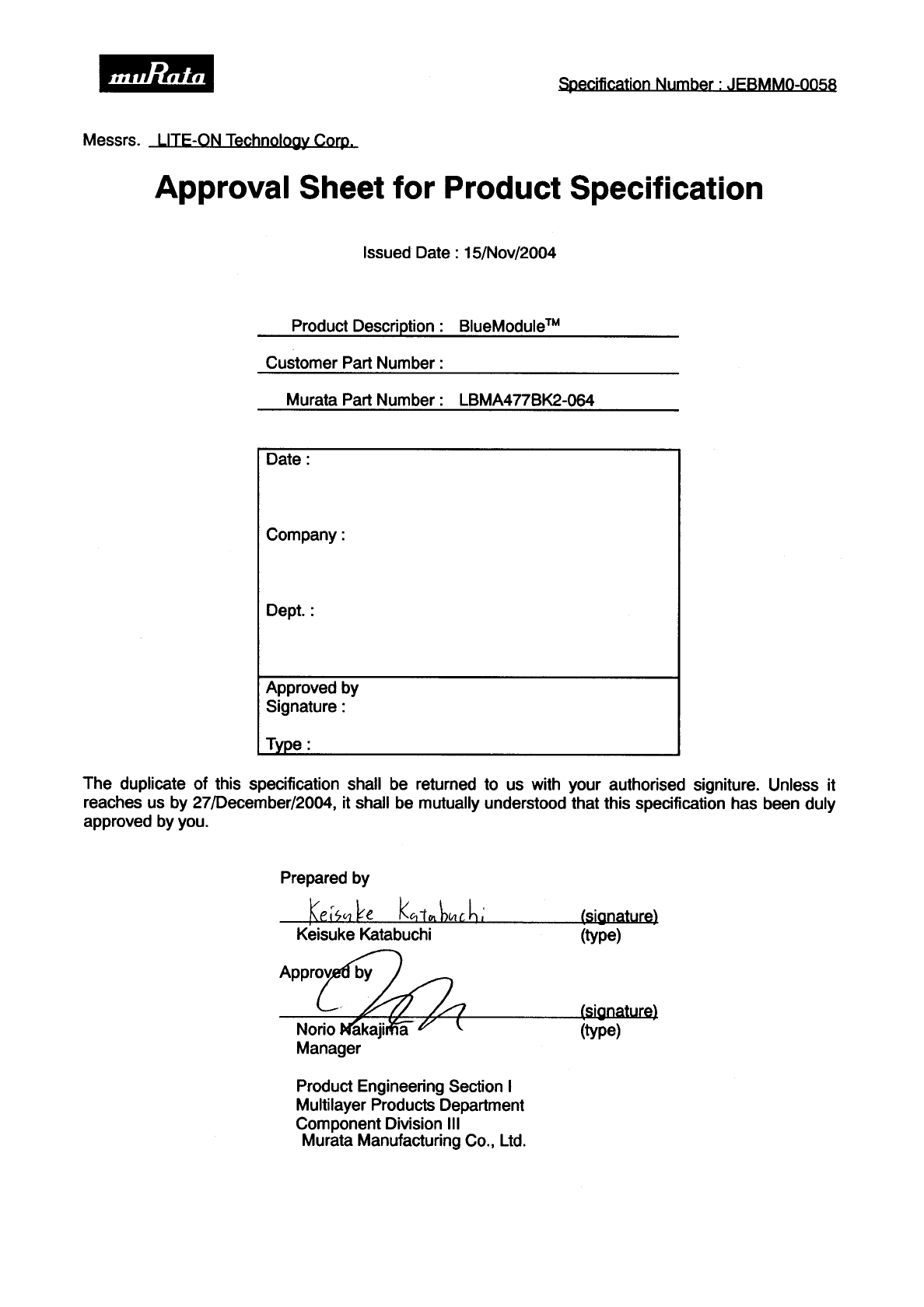
Specification Number : JEBMM0-0058
Messrs. LITE-ON Technology Corp.
Approval Sheet for Product Specification
Issued Date : 15/Nov/2004
Product Description : BlueModuleTM
Customer Part Number :
Murata Part Number : LBMA477BK2-064
Date :
Company :
Dept. :
Approved by
Signature :
Type :
The duplicate of this specification shall be returned to us with your authorised signiture. Unless it
reaches us by 27/December/2004, it shall be mutually understood that this specification has been duly
approved by you.
Prepared by
(signature)
Keisuke Katabuchi (type)
Approved by
(signature)
Norio Nakajima (type)
Manager
Product Engineering Section I
Multilayer Products Department
Component Division III
Murata Manufacturing Co., Ltd.
Specification Number : JEBMM0-0058
P.1/20
Murata Manufacturing Co., Ltd.
1. Scope
This specification is applied to the Bluetooth HCI module (Blue ModuleTM).
2. Part Number
Production Part Number LBMA477BK2-064
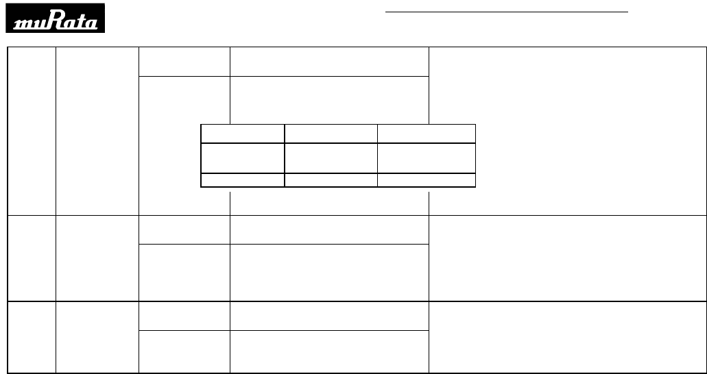
3. Rating
Ratings
Min Max Unit
Operating Temperature -20 +70 deg.C
Storage Temperature -40 +85 deg.C
Terminal Name Min Max Unit
BTRF_REG 2.2 V
BTL_REG 2.2 V
Supply Voltage
V_I_O 4.1 V
Input Terminal Voltage Vss-0.3 VDD+0.3 V
4. Weight (Nominal)
0.3g
Specification Number : JEBMM0-0058
P.2/20
Murata Manufacturing Co., Ltd.
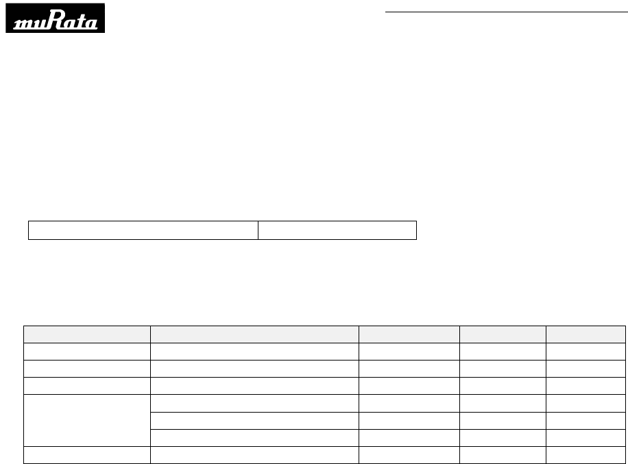
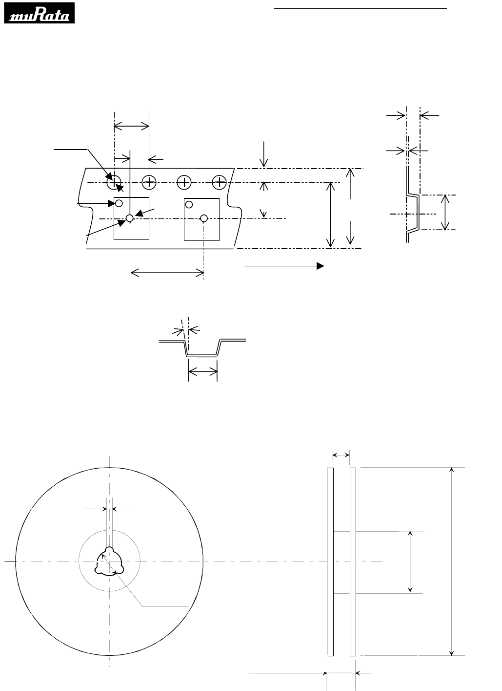
5. CONSTRUCTION, DIMENSIONS and Terminal Configurations
Mark Dimension Mark Dimension Mark Dimension
L7.5±0.2 W7.5±0.2 T 1.4 max
a1 0.4±0.2 a2 0.4±0.2 b1 0.75±0.2
b2 1.1±0.2 c1 0.6±0.2 c2 0.6±0.2
c3 4.9±0.2 c4 4.9±0.2 d1 0.75±0.2
d2 0.75±0.2 p1 0.7±0.2 p2 0.7±0.2
(Unit: mm)
<SIDE VIEW>
T
<SIDE VIEW>
(18)
(19) (20) (21) (22)
(23) (24) (25) (26)
(27)
(29)
(30)
(31)
(32)
(33)
(34)
(1)(2) (3) (4) (5)
(6) (7) (8) (9)
(10)
(11)
(12)
(13)
(15)
(16)
(17)
(14)
<BOTTOME VIEW>
(28)
c4
c3
c1
c2
b1
p1
b2
a2
p2
a1
(35)
d2
d1
(17)
W
Pin 1 index
<TOP VIEW>
L
(1)(1) (9)
(10)
(18)(26)
(27)
(34)
Lot Number
B
K
Specification Number : JEBMM0-0058
P.3/20
Murata Manufacturing Co., Ltd.
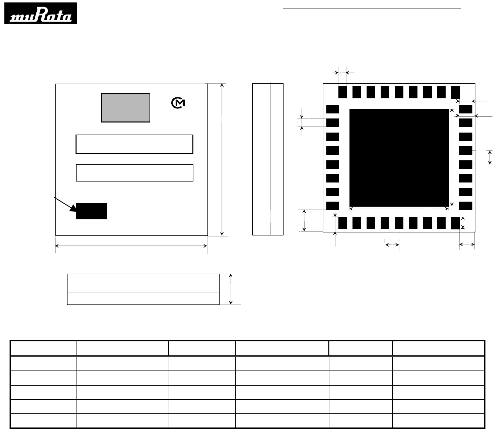
Terminal Configurations
Terminal
No.
Terminal Name Pin Type Description
(1) GROUND I -
(2) NC - -
(3) NC - -
(4) NC - -
(5) BLUE_TX I <UART_RXD> UART data input active
high
(6) REG_CTRL I Internal 1.8V regulator enable signal
(7) EEPROM_CLK O Clock interface to an optional serial
EEPROM
(8) NC -
(9) BLUE_HOST_WAKE O HOST_WAKE signal for power control
(10) V_I_O I -
(11) BLUE_WAKE I Active high or active low BT_WAKE
signal for powe control
(12) LPO_IN I 32.768KHz digital clock input
(13) BLUE_CLK_EN O -
(14) GROUND I -
(15) XTAL_OUT O Crystal Oscillator output
(16) XTAL_IN I Crystal or frequency reference input
(17) GROUND I -
(18) TM0 I Test Mode 0
(19) TM1_2 I Test mode 1 and 2
(20) TM3 I Test mode 3
(21) BTRF_REG I -
(22) RESET_N I Active LOW system reset
(23) TX_PU_TDD_N O Complement of TX_PU_TDD
(24) GROUND I -
(25) ANTENNA_MATCH I/O <Ant> RF input/output
(26) GROUND I -
(27) ASAP_CLK I/O <PCM_CLK> Synchronous data clock
(28) ASAP_FS I/O <PCM_SYNC> Synchronous data sync
(29) BLUE_CTS I <UART_CTS> UART clear to send
active low
(30) ASAP_RX O <PCM_OUT> Synchronous data output
(31) BLUE_RTS O <UART_RTS> UART request to send
active low
(32) ASAP_TX I <PCM_IN> Synchronous data input
(33) BLUE_RX O <UART_TXD> UART data output active
high
(34) BTL_REG I -
(35) GROUND I -
Specification Number : JEBMM0-0058
P.4/20
Murata Manufacturing Co., Ltd.
6. Electrical Characteristics
6-1 Operating Conditions
Min Typ Max Unit
Operating Temperature -20 +25 +70 deg.C
Supply Voltage
BTRF_REG, BTL_REG
V_I_O
1.71
1.71
1.8
2.8
1.98
3.63
V
V
6-2-1 Characteristics
+25degC,BTRF_REG/BTL_REG=1.8V, VIO=2.75V
Items Contents
Bluetooth specification Ver 1.2
Channel spacing 1MHz
Number of RF channel 79
Power class 2
Operation mode(Rx/Tx) Time division multiplex either transmit or receive
Frequency hopping after one Rx/Tx cycle
Items Min Typ Max Unit
1.Current Consumption
RF Register x57=xC6
1.1 BTRF_REG_IDC_max
DH5; 100% slot utilization;
50% Rx/Tx slot duty cycle
75 mA
1.3 V_I_O_REG_IDC_max
DH5; 100% slot utilization;
50% Rx/Tx slot duty cycle
10 mA
-TX characteristics- Min Typ Max Unit
2.Output Power -4 4 dBm
3.Frequency range(Rx/Tx)2400.5~2483.5MHz
4.-20dB bandwidth 1MHz
5.Adjacent Channel Power *1
5.1 [M-N]=2-21 dBm
5.2 [M-N]≧3-41 dBm
6.Modulation characteristics
6.1 Modulation δf1avg 145 173 kHz
6.2 Modulation δf2max 125 kHz
6.3 Modulationδf2avg/δf1avg 0.85
7.Initial Carrier Frequency Tolerance -45 45 kHz
8.Carrier Frequency Drift
8.1 1slot -25 25 kHz
8.2 3slot -40 40 kHz
8.3 5slot -40 40 kHz
8.4 Maximum drift rate -20 20 kHz/50μs
9.Out-of-Band Spurious Emissions
9.1 30-1000MHz (Operation Mode) -36 dBm
9.2 1000-12750MHz (Operation Mode) -30 dBm
9.3 1800-1900MHz(Operation Mode) -47 dBm
9.4 2110-2170MHz (Operation Mode) -75 dBm
9.5 5150-5300MHz (Operation Mode) -47 dBm
Specification Number : JEBMM0-0058
P.5/20
Murata Manufacturing Co., Ltd.
-RX characteristics- min typ max unit
10.Sensitivity (BER≦0.1%)
10.1 2402MHz -79 dBm
10.2 2441MHz -79 dBm
10.3 2480MHz -79 dBm
11.C/I Performance (BER≦0.1%) *2
11.1 co-channel ratio (-60dBm input) 11 dBm
11.2 1MHz ratio (-60dBm input) 0dBm
11.3 2MHz ratio (-60dBm input) -30 dBm
11.4 3MHz ratio (-67dBm input) -40 dBm
11.5 image ratio (-67dBm input) -9 dBm
11.6 image +/- 1MHz ratio (-67dBm input) -20 dBm
12.Blocking performance(BER<0.1%) *3
12.1 30MHz-2000MHz -10 dBm
12.2 2000MHz-2400MHz -27 dBm
12.3 2500MHz-3000MHz -27 dBm
12.4 3000MHz-12750MHz -10 dBm
13.Intermodulation performance
(BER≦0.1%, -64dBm input) -35 dBm
14.Maximum Input Level -20 dBm
*1 Up to three sprious responses within Bluetooth limits are allowed.
*2 Up to five sprious responses within Bluetooth limits are allowed.
*3 Up to twenty-four sprious responses within Bluetooth limits are allowed.
Specification Number : JEBMM0-0058
P.6/20
Murata Manufacturing Co., Ltd.
6-2-2. Extreme condition : -20 to +70degC, BTRF_REG/BTL_REG=1.71-1.98V, VIO=1.71-3.63V
Items Min Typ Max Unit
1.Current Consumption
RF Register x57=xC6
1.1 BTRF_REG_IDC_max
DH5; 100% slot utilization;
50% Rx/Tx slot duty cycle
80 mA
1.3 V_I_O_REG_IDC_max
DH5; 100% slot utilization;
50% Rx/Tx slot duty cycle
12 mA
-TX characteristics- Min Typ Max Unit
2.Output Power -6 +6 dBm
3.Frequency range(Rx/Tx)2400.5~2483.5MHz
4.-20dB bandwidth 1MHz
5.Adjacent Channel Power *1
5.1 [M-N]=2-20 dBm
5.2 [M-N]≧3-40 dBm
6.Modulation characteristics
6.1 Modulation δf1avg 145 175 kHz
6.2 Modulation δf2max 115 kHz
6.3 Modulationδf2avg/δf1avg 0.8
7.Initial Carrier Frequency Tolerance -75 75 kHz
8.Carrier Frequency Drift
8.1 1slot -25 25 kHz
8.2 3slot -40 40 kHz
8.3 5slot -40 40 kHz
8.4 Maximum drift rate -20 20 kHz/50μs
9.Out-of-Band Spurious Emissions
9.1 30-1000MHz (Operation Mode) -36 dBm
9.2 1000-12750MHz (Operation Mode) -30 dBm
9.3 1800-1900MHz(Operation Mode) -47 dBm
9.4 2110-2170MHz (Operation Mode) -65 dBm
9.5 5150-5300MHz (Operation Mode) -47 dBm
-RX characteristics- min typ max unit
10.Sensitivity (BER≦0.1%)
10.1 2402MHz -77 dBm
10.2 2441MHz -77 dBm
10.3 2480MHz -77 dBm
*1 Up to three spurious responses within Bluetooth limits are allowed.
Note
The above mentioned values have been obtained according to our own measuring methods (testing jig
Fig.1) and may very depend on the circuit, in which the component is actually incorporated. Therefore,
you are kindly requested to test the performance of the component actually in your set.
Specification Number : JEBMM0-0058
P.7/20
Murata Manufacturing Co., Ltd.
7. Other Specification and Methods
No. Items Specifications Test Methods
Appearance No severe damages1Vibration
Resistance
Electrical
Specification
s
Satisfy specifications listed in
paragraph 6.
Solder specimens on the testing jig shown in
appended Fig.3 by an solder. The soldering shall
be done either by iron or reflow and be
conducted with care so that the soldering is
uniform and free of defect such as by heat
shock.
Frequency : 10 to 2000 by 10 Hz
Acceleration : 196 m/s2
Direction : X,Y,Z 3axes
Period : 2 h on each direction
(Total 6 h.)
Appearance No severe damages2 Shock
Electrical
Specification
s
Satisfy specifications listed in
paragraph 6.
Solder specimens on the testing jig shown in
appended Fig.3 by an solder. The soldering shall
be done either by iron or reflow and be
conducted with care so that the soldering is
uniform and free of defect such as by heat
shock.
Pulse Wave : Sine Half Wave
Acceleration : 30000 m/s2 (Peak)
Period : 0.3 ms.
Cycle : 10 times
3 Deflection No damage with 1mm deflection Solder specimens on the testing jig shown in
appended Fig.3 by an solder. The soldering shall
be done either by iron or reflow and be
conducted with care so that the soldering is
uniform and free of defect such as by heat
shock.
4 Soldering strength
(Push Strength)
9.8 N Minimum Solder specimens on the testing jig shown in
appended Fig.3 by an solder. As shown below,
apply pushing force at 0.5 mm/s until electrode
pads are pealed off or ceramics are broken.
Pushing force is applied as show below.
5 Solderability of Termination 75% of the terminations is to be
soldered evenly and continuously.
Immerse specimens first a ethanol solution of
rosin (25% rosin in weight proportion), then in an
solder solution for 2+/-0.5 s at 230+/-5 deg.C.
Preheat : 100 to 120 deg.C, 60 s
Solder Paste : Eutectic Solder
Flux : Solution of ethanol and rosin
(25% rosin in weight proportion)
Appearance No severe damages6 Resistance
to Soldering
Heat
(Reflow)
Electrical
specifications
Satisfy specifications listed in
paragraph 6.
Preheat Temperature : 150 +/-10 deg.C
Preheat Period : 60s
Peak Temperature : 230+/-5 deg.C
Peak Temp. Period : 10 s
Specimens are soldered once with the above
condition, then kept in room condition for 24 h
before measurements.
No. Items Specifications Test Methods
Specimen
Jig
Pushing Direction
Specification Number : JEBMM0-0058
P.8/20
Murata Manufacturing Co., Ltd.
Appearance No severe damages7 Temperature
Cycle
Electrical
specifications
Satisfy specifications listed in
paragraph 6.
Set the specimens to the supporting jig in the
same manner and under the same condition as
Fig.1 and conduct the 100 cycles according to
the temperatures and time shown in the
following table.
Appearance No severe damages8 Humidity
Load Life
Electrical
specifications
Satisfy specifications listed in
paragraph 6.
Temperature : 85+/-2 deg.C
Humidity : 80 to 85%RH
Period : 500+24/-0 h
Room Condition : 2 to 24 h
Supply Voltage : 3.63V D.C. to V_I_O,
1.93V D.C to BTRF_REG and BTL_REG
Appearance No severe damages9 High Temp.
Load Life
Electrical
specifications
Satisfy specifications listed in
paragraph 6.
Temperature : 85+/-2 deg.C
Period : 500+24/-0 h
Room Condition : 2 to 24 h
Supply Voltage : 3.63V D.C. to V_I_O
1.93V D.C to BTRF_REG and BTL_REG
Excessive mechanical force or thermal stress may damage the products. Appropriate handling is
required.
8. Interface
UART
9. IC/Firmware
BROADCOM’s BCM2035 B3 Version
10. Production Site
FUKUI MURATA MFG.CO.,LTD.
Step 1 2
Temp.(deg.C) Min operating
Temp . + 0/-3
Max operating
Temp . + 3/-0
Time (min) 30+/-3 30+/-3
Specification Number : JEBMM0-0058
P.9/20
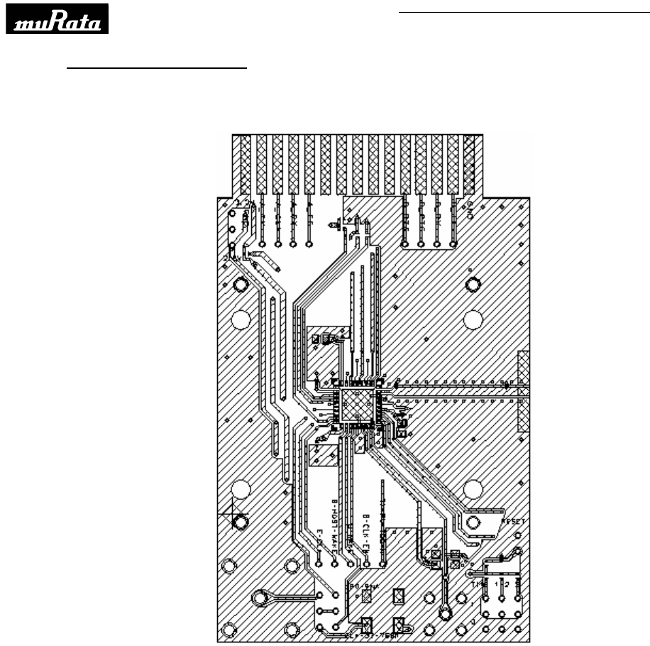
Murata Manufacturing Co., Ltd.
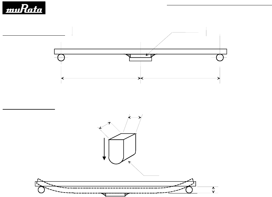
Fig.1 Measurement Board
Specification Number : JEBMM0-0058
P.10/20
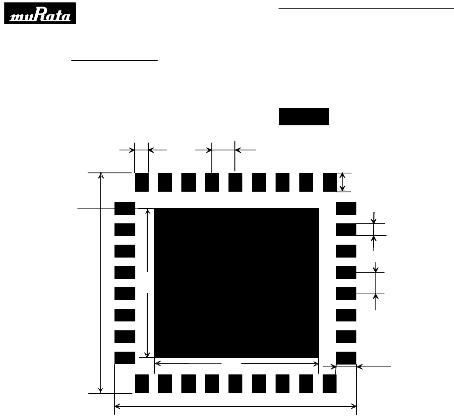
Murata Manufacturing Co., Ltd.
Fig.2 Land Patterns
(Unit:mm)
0.7
0.4
0.75
0.7
4.9
4.9
0.4
0.75
7.5
7.5
Land
Specification Number : JEBMM0-0058
P.11/20
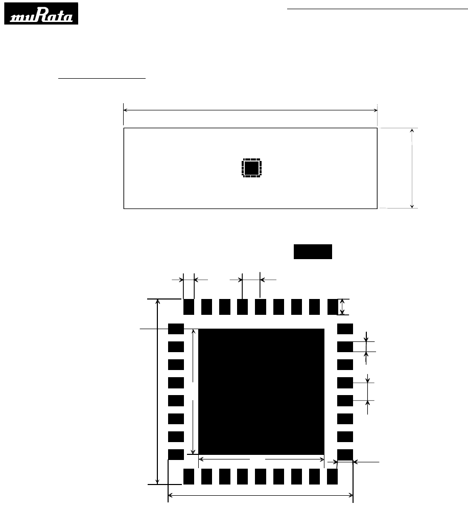
Murata Manufacturing Co., Ltd.
Fig.2 Testing Board
Unit:mm
Glass epoxy board t=0.8mm
Copper thickness 35um min
0.7
0.4
0.75
0.7
49
49
0.4
0.75
75
75
Land
40
100
Specification Number : JEBMM0-0058
P.12/20
Murata Manufacturing Co., Ltd.
Mounted Situation
Testing Method
100
Unit : mm
45 45
Module
R230
50
20
Deflection
Unit : mm
Specification Number : JEBMM0-0058
P.13/20
Murata Manufacturing Co., Ltd.
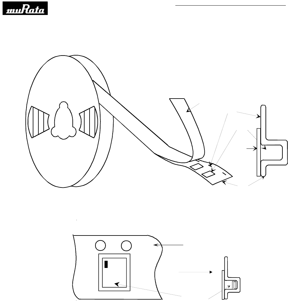
11.Tape and Reel Packing
(1) Dimensions of Tape ( Plastic tape )
1.Cumulative tolerance of max. ± 0.3 every 10 pitches
2.Reference value
(2) Dimensions of Reel
30.5 max.
(Unit :mm)
φ 13±0.2
2.0±0.5
25.5±0.6
100)
(
φ
330)
(
φ
4.0 ± 0.1
Min=14.25
2.0 ± 0.1
7.5 ± 0.1
16.0± 0.3
Max=0.6
1.6 ± 0.1
7.8 ± 0.1
12.0 ± 0.1
7.8 ± 0.1
Max 5.0°
Min=1.5
1.5+0.1
Feeding Direction
Pad 1
17.0±0.6
20.4 max
Specification Number : JEBMM0-0058
P.14/20
Murata Manufacturing Co., Ltd.
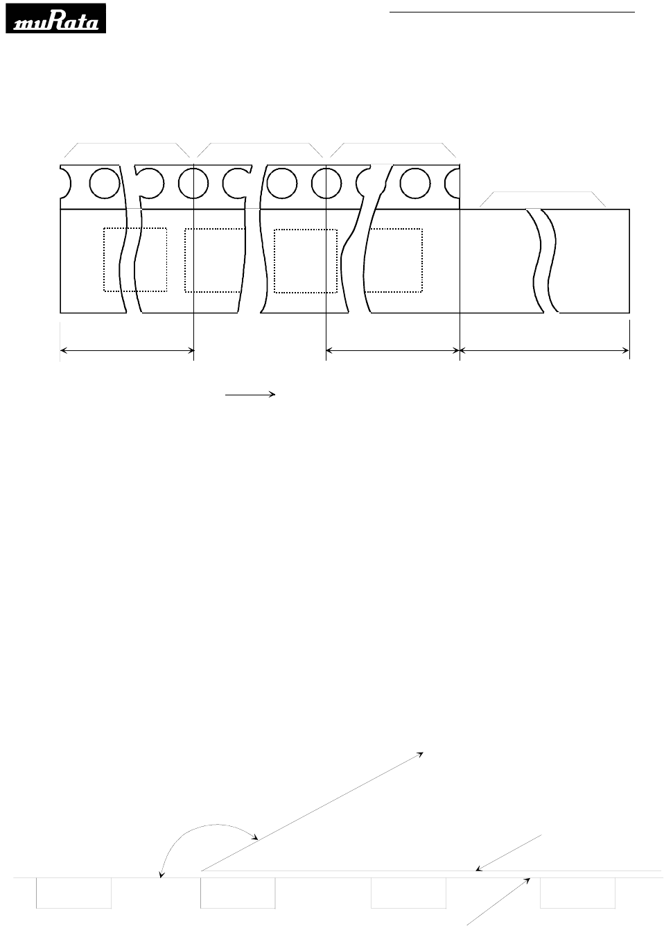
(3) Taping Diagrams
[1] Feeding Hole : As specified in (1)
[2] Hole for chip : As specified in (1)
[3] Cover tape : 62 μm in thickness
[4] Base tape : As specified in (1)
送り穴
[2]
[3]
[4]
[3]
[1]
送り穴
Module
Feeding Direction
Feeding Hole
Specification Number : JEBMM0-0058
P.15/20
Murata Manufacturing Co., Ltd.
(4) Leader and Tail tape
(5) The tape for chips are wound clockwise, the feeding holes to the right side as the ta
pe is pulled toward the user.
(6) The cover tape and base tape are not adhered at no components area for 250 mm min.
(7) Tear off strength against pulling of cover tape : 5 N min.
(8) Packaging unit : 1000 pcs./ reel
(9) material : Base tape : Plastic
Reel : Plastic
Cover tape , cavity tape and reel are made the anti-static processing.
(10) Peeling of force : 0.7 N max. in the direction of peeling as shown below.
165 to 180 °
0.7 N max.
Base tape
Cover tape
40 to 200 mm
Tail tape
(No components) Components No components
Feeding direction
Leader tape
(Cover tape alone)
150 mm min. 250 mm min.

Specification Number : JEBMM0-0058
P.16/20
Murata Manufacturing Co., Ltd.
NOTICE
1. Storage Conditions:
The product shall be stored under the following conditions in order not to damage the solderbility of the
external electrodes.
- The product shall be stored without opening the packing and at the ambient temperature between 5
and 30 deg.C and humidity between 20 and 70 %RH. And the product shall be used within 6 months
after reception. (Packing materials, in particular, may be deformed at the temperature over 45 deg.C.)
- After opening the packing, the product shall be stored at 5 to 30 deg.C / < 60 %RH and the product
shall be used within 48 hours. If the product is not used within 48 hours after opening the packing, the
product shall be baked under the following conditions.
Baking condition : 125 +/-5 deg.C, 24 hours, 1 time
The products shall be baked on the heat-resistant tray because the material (Base
Tape, Reel Tape and Cover Tape) are not heat-resistant.
- The product shall be stored in non corrosive gas (Cl2, NH3, SO2, Nox, etc.).
- Solderbility shall be confirmed before use if the product is stored for more than 3 months.
- When the indicator in the packing has changed its color, the product shall be baked before soldering.
- Any excess mechanical shock including, but not limited to, sticking the packing materials by sharp
object and dropping the product, shall not be applied in order not to damage the packing materials.
2. Handling Conditions:
- Be careful in handling or transporting products because excessive stress or mechanical
shock may break products due to the nature of ceramics structure.
- Handle with care because the characteristics of products may change if products may have cracks or
damages on their terminals. Do not touch products with bear hands that may result in poor
solderability.
3. Standard PCB Design (Land Patterns and Dimensions) :
- All the ground terminals should be connected to the ground patterns. Please refer to
Fig.2 for the standard land dimensions.
- The recommended land patterns and dimensions are as Murata's standard. The characteristics of
products may vary depending on the pattern drawing method, grounding method, land dimensions,
land forming method of the NC terminals and the PCB material and thickness. Therefore, be sure to
verify the characteristics in the actual set. When using non-standard lands, contact Murata
beforehand.
4. Notice for Chip Placer :
- When placing products on the PCB, products may be stressed and broken by uneven
forces from a worn-out chucking locating claw or a suction nozzle. To prevent products
from damages, be sure to follow the specifications for the maintenance of the chip placer
being used. For the positioning of products on the PCB, be aware that mechanical
chucking may damage products.
Specification Number : JEBMM0-0058
P.17/20
Murata Manufacturing Co., Ltd.
5. Soldering Conditions :
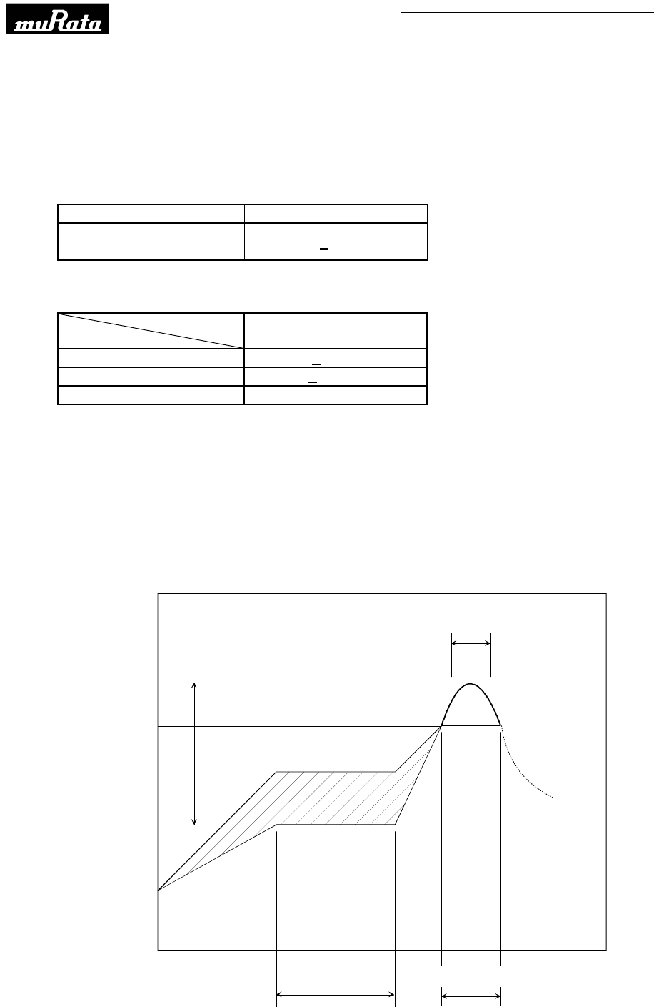
- Carefully perform preheating so that the temperature difference (delta T) between the solder and
products surface should be in the following range. When products are immersed in solvent after
mounting, pay special attention to maintain the temperature difference within 100 deg.C. Soldering
must be carried out by the above mentioned conditions to prevent products from damage. Contact
Murata before use if concerning other soldering conditions.
Soldering methods Temperature
Soldering iron method
Reflow method delta T < 130 deg.C
- Soldering iron method conditions are indicated below.
Kind of iron
Items Ceramic heater
Soldering iron wattage < 18 W
Temperature of iron-tip <350 °C
Iron contact time within 3 s
- Diameter of iron-tip : φ3.0 mm max.
- Do not touch the module itself directly by the iron-tip.
within 3 s.
within 120 s
∆Τ
Temperature (°C)
Pre-heating
Time (s.)
Reflow soldering standard conditions(Example)
220 °C
within 60 s.
Cooling down
slowly
250 to 260 °C
Specification Number : JEBMM0-0058
P.18/20
Murata Manufacturing Co., Ltd.
- Use rosin type flux or weakly active flux with a chlorine content of 0.2 wt% or less. Be careful so as
not to remain the flux residue around products. Because there are possibilities to become worse the
characteristics.
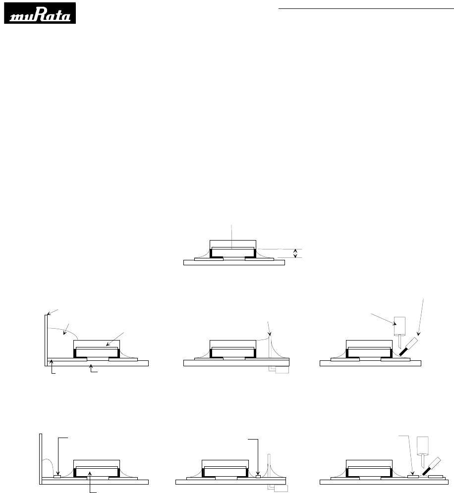
- Amount of Solder Paste:
Ensure that solder is applied smoothly to a minimum height of 0.2 to 0.5 mm at the end surface of
the external electrodes. If too much or little solder is applied, there is high possibility that the
mechanical strength will be insufficient, creating the variation of characteristics.
Amount of solder paste
Chip
Hight
<Unacceptable>
<Improvements by land division>
Lead wire of leaded
component Soldering iron
Lead wire of componen
mounted later
Solder resist Solder resist Solder resist
Chip
Chassis
Solder (Grounding solder)
Chip
Land PCB

Specification Number : JEBMM0-0058
P.19/20
Murata Manufacturing Co., Ltd.
6. Operational Environment Conditions :
- Products are designed to work for electronic products under normal environmental conditions
(ambient temperature, humidity and pressure). Therefore, products have no problems to be used
under the similar conditions to the above-mentioned. However, if products are used under the
following circumstances, it may damage products and electric shock and abnormal temperature may
occur.
- In an atmosphere containing corrosive gas (CL2, NH3, SOx, NOx, etc.).
- In an atmosphere containing combustible and volatile gases.
- Dusty place.
- Direct sunlight place.
- Water splashing place.
- Humid place where water condenses.
- Freezing place.
- If there are possibilities for products to be used under the preceding clause, consult
with Murata before actual use.
- As it might be a cause of degradation or destruction to apply static electricity to
products, do not apply static electricity or excessive voltage while assembling and
measuring.
7. Limitation of Applications :
Please contact Murata before using products for the applications listed below which
require especially high reliability for the prevention of defects which might directly cause
damage to the third party's life, body or property.
- Aircraft equipment.
- Aerospace equipment.
- Undersea equipment.
- Medical equipment.
- Transportation equipment (vehicles, trains, ships, etc.).
- Traffic signal equipment.
- Disaster prevention / crime prevention equipment.
- Data-processing equipment
- Application of similar complexity and/ or reliability requirements to the applications listed in the
above.
Specification Number : JEBMM0-0058
P.20/20
Murata Manufacturing Co., Ltd.
Note :
- Please make sure that your product has been evaluated and confirmed against your specifications
when our product is mounted to your product.
- All the items and parameters in this product specification have been prescribed on the premise that
our product is used for the purpose, under the condition and in the environment agreed upon between
you and us. You are requested not to use our product deviating from such agreement.
- We consider it not appropriate to include other terms and conditions for transaction warranty in
product specifications, drawings or other technical documents. Therefore, even if your original part of
this product specification includes such terms and conditions as warranty clause, product liability
clause, or intellectual property infringement liability clause, we are not able to accept such terms and
conditions in this product specification unless they are based on the governmental regulation or what
we have agreed otherwise in a separate contact. We would like to suggest that you propose to discuss
them under negotiation of contract.