Baron Services DSSR-250C Pulsar Digital Solid-State Radar System User Manual
Baron Services Inc Pulsar Digital Solid-State Radar System
Contents
Hardware Installation
Hardware Installation
RVP8 User’s Manual
September 2005
2–1
2. Hardware Installation
2.1 Overview and Input Power Requirements
This chapter describes how to install the RVP8 hardware. Topics include mechanical installation
and siting, electrical specifications of the interface signals, system-level considerations and the
standard connector panel that is provided.
There are three major modules supplied with the RVP8. These are:
IFD (IF Digitizer) Typically mounted in the radar receiver cabinet.
Input Power 47–63 Hz 100–240 VAC Auto-ranging
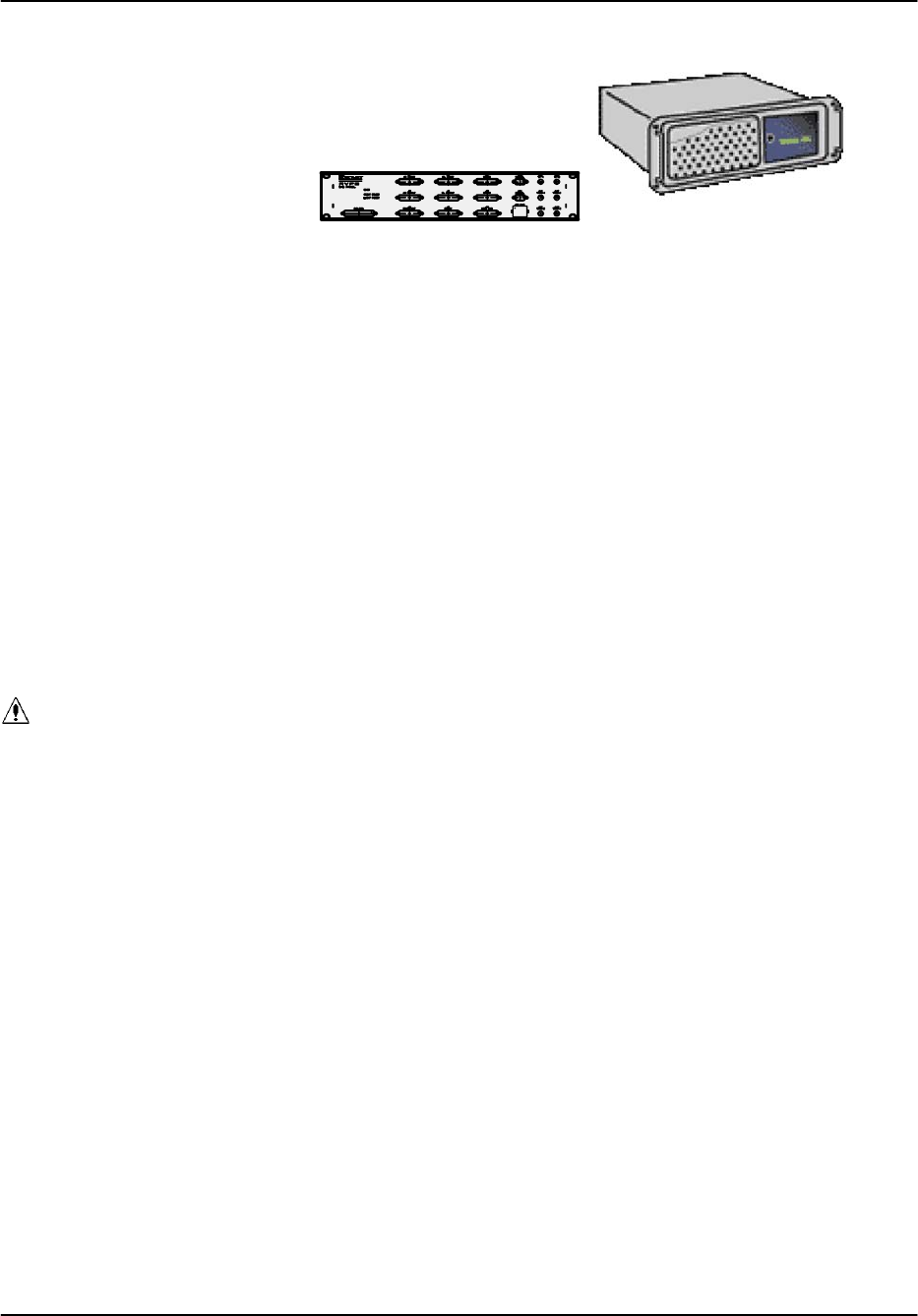
Main Chassis Usually mounted in 19” EIA rack.
Input Power 60/50 Hz 115/230 VAC Manual Switches
I/O-62 Connector Panel
Usually mounted in 19” EIA rack within 2 m of Main Chassis
Much of the RVP8 I/O is configured via software. This makes the unit very flexible. Also, since
there is virtually no custom wiring, it is very easy to insert spare modules and circuit cards. The
software configuration of the I/O is described in Appendix A.
This section, in conjunction with Appendix B, describes the physical installation of the
hardware.
WARNING: The Main Chassis redundant power supplies are NOT auto-ranging
like the IFD. These are factory configured for the expected voltage, but should
be VERIFIED by the customer before power is applied to the system.
Hardware Installation
RVP8 User’s Manual
September 2005
2–2
2.2 IFD IF Digitizer Module Installation
The IFD mains power is to be permanently “hard wired” in a NEMA electrical
enclosure that is accessible only to a trained technician. The ground (earth)
connection should be attached directly to the IFD case mounting screw then
brought to the power supply ground connection.
Disconnect the the mains power before opening the IFD for service. The IFD is
best serviced by disconnecting the mains power, removing it from its mount and
placing it on a bench.
2.2.1 IFD Introduction
The IFD IF digitizer is housed in an electrically sealed solid metal enclosure to achieve good
immunity to external electrical noise. The internal circuitry has been designed to minimize the
number of digital components, and it is carefully grounded and shielded to make the cleanest
possible samples of the input IF signal. The unit is cooled by direct conduction of heat through
the metal chassis; there are no openings required for airflow.
The IFD replaces all of the IF receiver components that are found in a traditional analog receiver
system, i.e.,
SBand Pass Filters
SLOG Receiver
SAFC Circuit
SAGC or IAGC circuit
SQuad Phase Detector
SCOHO (on magnetron systems)
SLine drivers for base band video
Indeed, one of the most time consuming parts of an upgrade is often the removal of old
components. Many customers choose to simply bypass them and leave them in place. In some
cases there will be other receiver modifications required to match the IFD signal input
specifications. For example, IF attenuators or an IF amplifier are sometimes required.
If you are doing an upgrade of an older system, you might want to consider
purchase of a new STALO which can make significant improvements in Doppler
performance.
You should carefully document and red-line your system schematics to reflect any changes to the
receiver.

Hardware Installation
RVP8 User’s Manual
September 2005
2–3
2.2.2 IFD Revision History
There have been several hardware revisions of the IFD module since its introduction initially
with the RVP7. Table 2–1 summarizes the differences among all of the versions that have been
manufactured so far. The remainder of this chapter covers only the 14-bit units, although the
previous generation 12-bit units are compatible with the RVP8 as well.
Table 2–1: Differences Among Versions of the IFD
Rev.B Rev.C Rev.D Rev.E & Higher
A/D Chip Analog Devices AD9042, 12–Bits AD6644, 14–Bits AD6645, 14–Bits
Nominal IF
Sample Rate 36MHz 72MHz
IF Inputs Single IF Input Channel Dual IF Inputs
A/D Noise
Density –76dBm/MHz –82dBm/MHz –85dBm/MHz
Dynamic
Range 86dB at 0.5MHz 93dB at 0.5MHz 96dB at 0.5MHz
Link to Rx Coax uplink, Fiber downlink Integrated CAT-5E
Upgradability FPGA chips must be manually reprogrammed ReFlashable via Rx-Link
Input Signal
Level A/D saturation at +4.5dBm A/D saturation at +6.0dBm
Ext-Clock No Yes (shared with AFC connector)
Noise
Generator
None. The A/D dither power must
be supplied from wideband thermal
noise in the RF/IF chain.
Built-in noise source supplies A/D dither power in the
200–900KHz range.
Power Supplies +5.17V, +12V, –12V +5.23V Primarily.
+12/15V required only for
analog AFC output
+5.33V Primarily.
+12/15V required for
AFC, Hi-DAFC or stable
VCXO (recommended).
–12/15V required only for
analog AFC output.
Jumpers
(Table 2–7) None AFC/Clock I/O AFC/Clock I/O,
Dither and Config
Selections
AFC/Clock I/O, JTAG,
DAFC/Clock and Config
Selections
Uplink
Protocols AFC-16 AFC-16 &
PLL-16 Supports full set of protocols defined in Section 2.5.1
First
Production March 1997 April 1998 December 2000 August 2004

Hardware Installation
RVP8 User’s Manual
September 2005
2–4
2.2.3 IFD Power, Size and Mounting Considerations
The IFD is a compact sealed module with dimensions 23.6 x 10.9 x 3.0 cm. (9.3 x 4.3 x 1.2 in).
The unit is designed to be mounted on edge such that the 23.6 x 3.0 cm. surface is flush on the
back of the receiver cabinet with 10.9 cm. protrusion into the cabinet. The unit is typically
placed where a traditional LOG receiver would be installed. The IFD is cooled by direct
conduction through its metal enclosure. It should be positioned so that air can freely convect
around it, or bolted to a larger surface that will conduct the heat away.
The power supply module is separate and can be mounted nearby in the radar cabinet, or it can
be attached directly to the IFD using a special mounting bracket. The power supply and bracket
will add 3.3 cm. (1.3 in) of overall width to the receiver module.
The power supply is a low noise, low ripple, switching unit; the input voltage range is 100–240
VAC 47–63 Hz, autoranging. The IFD has an internal 3-stage power supply input filter to
minimize interference from the power cable. Nonetheless, it is still good practice to insure that
the four supply wires (+5V, –12V, +12V, and Ground) be kept short and twisted together. A
ferrite choke around the supply wires near the terminal strip is also recommended.
Important: The inductive filtering components inside the IFD introduce a
voltage drop in the +5V supply. To produce the correct internal voltage, the
supply voltage measured at the external terminal block should be 5.33V for
Rev.E and later, 5.23V for Rev.D, and 5.17V for Rev.C and earlier boards.
Important: The voltage drop across the inductive filtering components causes
the ground terminal of the power supply to float several tenths of a volt above
chassis ground. For this reason, the IFD power supply should never be tapped
to supply power to other nearby equipment.
Mounting space should also be reserved for the external analog anti-alias filters. These filters
can be mounted in the radar cabinet itself, or they can be attached directly to the IFD on the
opposite side of the power supply. The filters and mounting bracket will add 2.0 cm. (0.8 in) of
overall width.
The 72MHz CAT-5E IFD (Rev.F) represents a factor–of–two improvement in A/D sampling rate
and communications bandwidth between the IFD and RVP8/Rx card. This provides important
advantages in the performance of your radar system, but it does also place greater demands on
the connecting link. The CAT-5E cable carries real–time 1.080MBaud downlink serial data on
three of its four twisted pairs, and uses the fourth pair for uplink communication. The data rate
on each downlink pair actually exceeds the data rate for GigaBit ethernet, hence very high
quality cable must be used, and maximum cable length is limited to 25-meters. There is also a
minimum cable length of 2-meters.
We recommend using a shielded CAT–5E cable (certified to >= 350MHz) having shielded RJ45
plugs on each end. The Rx board provides a DC return path for the cable shield, while the IFD
provides an AC GND only (isolated to 2KV). This design prevents ground loop currents from
flowing between units, even when they’re plugged into different AC/Mains.

Hardware Installation
RVP8 User’s Manual
September 2005
2–5
2.2.4 IFD I/O Summary
The connectors on the IFD are labelled and described below for each hardware revision.
Table 2–2: IFD Connectors (All Revisions)
IFD I/O Summary
Connector
Label
Style Description Reference
J1
IFĆIN
SMA IF signal from LNA/mixer; via an antiĆaliasing filter
centered at IF (supplied by SIGMET). 50W, + 6.5 dBm
max
2.2.6
2.2.7
2.2.8
2.2.10
J2
BURST
(COHO)
SMA IF Tx sample from waveguide tap and mixer; via an
antiĆaliasing filter centered at IF (supplied by SIGĆ
MET). 50W, +6.5 dBm max
2.2.6
J3
AFC
(CLK)
SMA AFC output (+-10V) or reference clock input for coĆ
herent systems (2-60 MHz -10 to 0 dBm). The funcĆ
tion of the connector is controlled by jumper selecĆ
tion within the IFD.
2.2.11 AFC
2.2.12 CLK
Since they share the same connector, analog AFC output and reference clock input can not be
used simultaneously. However, this is a very rare requirement since an analog AFC output is
used for magnetron systems and a reference clock input is typically used for fully coherent TWT
and Klystron systems.
Table 2–3: IFD Connectors (Rev.A–Rev.D)
IFD I/O Summary
Connector
Label
Style Description Reference
J4
UPLINK
SMA/BNC Connects to the RVP8/Rx PCI card by 75 Ohm
shielded cable. The connector is SMA with an SMA/
BNC adapter provided.
2.2.13
J5
FIBERĆOUT
ST 62.5/125 micron multimode optical cable terminated
in type ST connectors. IFD cam be located up to
100m from the RVP8/Rx PCI card.
2.2.13
Table 2–4: IFD Connectors (Rev.E & Greater)
IFD I/O Summary
Connector
Label
Style Description Reference
J4
DAFC(CLK)
SMA Synthesized legacy coax uplink stream for backward
compatibility, or Expansion Clock input or output.
2.2.13
J5
RxĆLink
RJĆ45 Connects to the RVP8/Rx PCI card via CATĆ5E cable
up to 25Ćmeters in length.
2.2.13

Hardware Installation
RVP8 User’s Manual
September 2005
2–6
2.2.5 IFD Adjustments and Test/Status Indicators
The IFD is packaged in a tight metal enclosure for maximum noise immunity. The only
adjustments on the module are the internal gain and offset pots that adjust the AFC analog
output. Two switches on the unit provide standalone test features to verify the proper functioning
of the IFD and to assist with setting the voltage span of the AFC DAC.
Table 2–5: IFD Toggle Switch Settings
SW1 SW2 Function
A A AFC Test Low Voltage
A B AFC Test Midpoint Voltage
A C AFC Test High Voltage
B A Swap Burst and IF Input Signals
B B Normal Operation (also labeled as “run”)
B C Reserved (downlink test pattern)
C A Reserved
C B Reserved (downlink test pattern)
C C Reserved (downlink test pattern)
Two LEDs provide status information for the IFD itself, as well as status of the communication
link(s) to the RVP8/Rx PCI card. These LEDs have the same interpretation across all revisions
of the IFD. For Rev.B through Rev.D the words “uplink” and “downlink” refer to the physical
coax uplink and fiber downlink cables. For Rev.E and higher, those words refer to conceptually
similar uses of the four twisted pairs within the integrated CAT-5E link.
Table 2–6: IFD LED Indicator Interpretations
Red (Uplink) Green (Ready) Meaning
Blink Blink Reset sequence (powerup, or from uplink)
Blink Off Uplink is dead (no uplink protocol from RVP8/Rx)
On Off Uplink is alive, but downlink is dead
On On Normal Operation (IFD and Main are both okay)
For IFDs at Rev.E and higher, the two LEDs on the RJ-45 connector also convey status about the
CAT-5E link itself. Green indicates that valid clock and framing waveforms are present on the
uplink. Yellow indicates that the RVP8/Rx card is receiving valid data from the IFD, including
the IFD’s report of the uplink being okay. These LEDs show valid status at all times (not just
when the RVP8 software is running) and thus, both indicators should be illuminated whenever
the CAT-5E cable is connected. Moreover, the Green/Yellow interpretation is consistent at both
the IFD and RVP8/Rx ends: green indicates the reception of proper low-level electrical and

Hardware Installation
RVP8 User’s Manual
September 2005
2–7
framing protocols, and yellow indicates that the green LED is ON at the other end, i.e., that the
other end is receiving our transmissions correctly and is able to communicate that information
back to us.
The internal jumper settings are summarized in the following table. Please also refer to Sections
2.2.11 and 2.2.12 for more information on setting up the AFC or External Clock options.
Table 2–7: IFD Internal Jumper Settings
Rev.B Rev.C Rev.D Rev.E and Higher
JP1 N/A AB: AFC Voltage Output
BC: External Clock Input, 50W Termination
Open: External Clock Input, No Termination
JP2 N/A Reserved (Open) AB: Normal JTAG control
BC: Factory reserved
JP3 N/A AB: Unused
BC: External Clock
Open: AFC Voltage Output
Power Supply to Oscillator
Use wirewrap, not jumper
AB: Regulated from +12V
BC: Direct from +5V
JP4 N/A AB: Dither Applied to Burst
BC: No Dither on Burst AB: Oscillator is a VCXO
BC: Oscillator is fixed XO
JP5 N/A Reserved for factory tests
Must be left open
JP6 N/A J4 Protocol Selector
AB: Legacy DAFC output
BC: Auxiliary CLK In/Out
JP7 N/A J4 DAFC Output Level
AB: +5V Signaling
BC: +12V Signaling

Hardware Installation
RVP8 User’s Manual
September 2005
2–8
2.2.6 IFD Input A/D Saturation Levels
There are two analog signals that must be supplied to the IFD:
SIF receiver signal
SIF Tx Sample (Burst Pulse) for magnetron, or COHO reference for klystron.
Both of these inputs are on SMA connectors. The IF signal should be driven by the front-end
mixer/LNA/IF-Amp. components, similar to the way that a LOG receiver would normally be
installed. The magnetron burst pulse or klystron COHO reference is also derived in the same
manner as a traditional analog receiver.
Note: Even for fully coherent Klystron and TWT systems, SIGMET
recommends the use of an actual IF Tx sample. If this is not possible, then the
COHO itself may be used instead. If there is phase modulation, then the
phase-shifted COHO should be input.
The A/D input saturation level for both the IF-Input and Burst-Input is +6 dBm (4.5 dBm for
Rev.C or earlier). In almost all installations an external anti-alias filter is installed on both of
these inputs. These filters (if supplied by SIGMET) are mounted externally on one side of the
IFD, and have an insertion loss of approximately 1–2dB. Thus, the input saturation level will be
+8dBm measured at the filter inputs.
For the burst pulse or COHO reference it is important not to exceed the A/D saturation level.
This reference signal should be strong enough so that most of the bits in the A/D converter are
used effectively, but it should also allow a few deciBels below the saturation level for safety.
The recommended power level is in the range –12 to +1 dBm, measured as described in section
D.14. This is important for making a precise phase measurement on each pulse.
In contrast, for the IF receiver input it is permissible (in fact desirable) to occasionally exceed
the A/D input saturation level at the strongest targets. The RVP8 employs a statistical
linearization algorithm to derive correct power levels from targets that are as much as 6dB above
saturation. The actual IF signal level should be established by weak-signal and noise
considerations (see below), rather than by working backwards from the saturation level.

Hardware Installation
RVP8 User’s Manual
September 2005
2–9
2.2.7 IF Bandwidth and Dynamic Range
The RVP8 performs best with a wide bandwidth IF input signal. This is because a wideband
signal can be made free of phase distortions within the (relatively narrow) matched passband of
the received signal. The RVP8 uses an external analog anti-aliasing filter at each of its IF and
Burst inputs. The purpose of these filters is to block frequencies that would otherwise alias into
the matched filter passband. The anti-alias filters have a nominal passband width of 14 MHz
centered at 30MHz, i.e. from 23MHz to 37MHz. This is the recommended operating bandwidth
for the IF signal, although the RVP8 will still work successfully with lesser IF bandwidth.
At the 36MHz sampling rate the quantization noise introduced by LSB uncertainties is spread
over an 18MHz bandwidth. For an ideal 14-bit A/D converter that saturates at +6dBm the
effective quantization noise level would be:
)6dBm *20log10(214)*10log10(18MHz
1MHz )+*90dBm (at 1MHz BW)
If samples from this ideal converter were processed with a digital filter having a bandwidth of
1MHz, then an input signal at –90dBm would have a signal-to-noise ratio of 0dB. A narrower
FIR passband (corresponding to a longer transmitted pulse) would decrease the quantization
noise even further, so that 0dB SNR would be achieved at even lower input power.
In practice, the 14-bit A/D converter used inside the IFD does not behave quite this well. The
Analog Devices AD6644 chip has been measured to have a wideband SNR of 76dB, i.e., 8dB
less than the 84dB range expected for an ideal converter. The above calculation for noise
density thus becomes:
)6dBm *76dB *10log10(18MHz
1MHz )+*82dBm (at 1MHz BW)
Indeed, the RVP8’s receiver power monitor described in Section 4.5 will show a filtered power
level of approximately –82dBm when the FIR bandwidth is 1MHz and the IFD inputs are
terminated in 50–Ohms.
The inverse correspondence between filter bandwidth and the 0dB SNR signal level leads to an
interesting and useful property of wideband digital receivers: they can operate over a dynamic
range that is much greater than the inherent SNR of their A/D converter would imply. If this
particular A/D chip were performing direct conversion at “base band” it would have a dynamic
range of only 76dB. However, by utilizing the extra bandwidth of the converter, the RVP8 is
able to extend the dynamic range to approximately 100dB.
To understand this, begin with the 88dB interval between the converter’s +6dBm saturation level
and the –82dBm 0dB SNR level at 1MHz bandwidth. Add to this:
S6dB for the statistical linearization that is performed on signals that exceed the saturation
level. The RVP8 can recover signal power accurately even when the A/D converter is
driven beyond saturation. Velocity data will also be valid, but spectral width may be
overestimated.
S4dB for usable dynamic range below the 0dB SNR level. In practice, a coherent signal at
–4dB SNR can easily be measured when 25 or more pulses are used.
Hardware Installation
RVP8 User’s Manual
September 2005
2–10
Thus, the overall dynamic range at 1MHz bandwidth (approx. 1 msec transmit pulse) is 88+6+4
= 98dB. For a 0.5 msec pulse the dynamic range would be reduced to 95dB; but it would
increase to 101dB for a 2.0 msec pulse. An actual calibration curve demonstrating this
performance is shown in Figure 2–1, for which the RVP8’s digital bandwidth was set to
0.53MHz and external signal generator steps of 1dB were used over the full operating range.
Figure 2–1: Calibration Plot for a Stand-alone 14-Bit IFD
–100
–90
–80
–70
–60
–50
–40
–30
–20
–10
0
10
20
–100 –90 –80 –70 –60 –50 –40 –30 –20 –10 0 10 20
1-dB Detection Threshold
Input Power in dBm Measured at IFD IF-Input
1-dB Compression Point
Overall Dynamic Range of 101dB
Hardware Installation
RVP8 User’s Manual
September 2005
2–11
2.2.8 IF Gain and System Performance
The previous discussion was concerned with measuring the dynamic range of a stand-alone IFD.
We will now examine how the unit performs in the context of a complete radar receiver. We
assume that an LNA/Mixer has already been selected that offers an appropriate balance between
price and noise figure. Having chosen these front-end components, the only parameter that
remains to be determined is the total RF/IF gain between the antenna waveguide and the IFD.
Assume that the thermal noise (kT) of the system is –114dBm/MHz, and that the noise figure of
the LNA/Mixer is 2dB. We wish to bring this –112dBm/MHz noise level up into the working
range of the IFD so that the received echoes can be optimally processed. However, in trying to
select the required gain, we realize that we must make a tradeoff between preserving the receiver
sensitivity that has been established by the LNA, and preserving the overall dynamic range of
the IFD. This is the exact same tradeoff that is made in traditional multi-stage analog receiver
systems that include a wide dynamic range LOG receiver.
0
1
2
3
4
5
6
7
8
9
10
012345678910
Reduction of Receiver Sensitivity (dB)
Reduction of IFD Dynamic Range (dB)
Figure 2–2: Tradeoff Between Dynamic Range and Sensitivity
Recommended
Operating Region
Power Ratio R = 10log10( NLNA / NIFD )
The solid red curve in Figure 2–2 shows that these two variables interact in a symmetric manner,
so that any operating point (x,y) is always matched by a dual operating point at (y,x). To
understand the construction of this plot, let NIFD represent the stand-alone (terminated input)

Hardware Installation
RVP8 User’s Manual
September 2005
2–12
noise power of the IFD over some bandwidth. Similarly, let NLNA represent the LNA/Mixer
thermal noise power over that same bandwidth, and after amplification by all RF and IF stages.
Note that NIFD is primarily due to the quantization noise that is introduced by the A/D converter,
whereas NLNA has its origins in the fundamental thermal noise of the receiving system. The
reduction of receiver sensitivity is the amount by which the LNA thermal noise is increased over
the original level established by the front-end components:
DSensitivity +10 log10(NLNA )NIFD )*10 log10(NLNA )+10 log10ǒ1)NIFD
NLNAǓ
Likewise, the reduction of RVP8 dynamic range is the amount by which the IFD quantization
noise is increased over its stand-alone value:
DDynamicRange +10 log10(NLNA )NIFD )*10 log10(NIFD )+10 log10ǒ1)NLNA
NIFDǓ
Note that both of these quantities depend only on the ratio of the two powers; hence, the two
equations define a parametric relationship in the dimensionless variable R+(NLNA ńNIFD ).
Figure 2–2 was created by sweeping the value of R from 1/9 to 9. The solid red curve shows the
locus of ( DDynamicRange,DSensitivity ) points, and the dashed green curve shows R itself
(expressed in dB) as a function of DDynamicRange. For example, when the LNA noise power
is equal to the IFD noise power, R is 1.0 (0dB) and there will be a 3dB reduction in both
sensitivity and dynamic range.
The recommended operating region is the portion of the curve that limits the loss of sensitivity
to between 1.4dB and 0.65dB. The attendant loss of dynamic range will fall between 5.5dB and
8.5dB respectively. Each axis of the plot has an important physical interpretation within the
radar system.
SThe horizontal axis is equivalent to the increase in the RVP8’s report of filtered power
when the IF-Input coax cable is connected versus disconnected. This is an easy quantity
to measure, and thus provides a simple way to check the overall gain of the
LNA/Mixer/IF components.
SThe vertical axis is equivalent to a worsening of the LNA/Mixer noise figure. This can
also be interpreted as the amount of transmit power that is, in some sense, “wasted” when
observing very weak echoes. If you have installed an expensive LNA with a very low
noise figure, then you will want to pick an operating point that makes the most of
preserving that investment.
Figure 2–2 can be used to calculate the net gain that is required by the front-end components,
and to predict the final system performance:
1. Choose an operating point that balances your need for sensitivity versus dynamic
range. For this example, we will allow a 1dB loss of sensitivity from the
theoretical limit of the LNA/Mixer, and will assume a bandwidth of 0.5MHz.
2. For a 1dB loss of sensitivity, the DDynamicRange is first determined from the
solid red curve as 7dB. The required noise ratio R is then read vertically on the
dashed green curve as 6.1dB.

Hardware Installation
RVP8 User’s Manual
September 2005
2–13
3. Thus, the RF/IF gain must bring the front-end thermal noise at –112dBm/MHz up
to a level that is 6.1dB higher than the IFD noise density of –82dBm/MHz. The
gain is therefore (–82dBm/MHz + 6dB) – (–112dBm/MHz) = 36dB. Note that
this gain does not depend on bandwidth, and therefore will be correct for all
pulsewidth/bandwidth combinations.
4. The dynamic range for the complete system at 0.5MHz bandwidth may now be
calculated as 101dB – 7dB = 94dB.
5. After assembling all of the RF and IF components we can check whether we
achieved the correct gain by verifying a 7dB rise (independent of bandwidth) in
RVP8 filtered power when the IF-Input cable is connected versus disconnected.
Keep in mind when designing your RF and IF components that the final amplifier driving the
IFD must be capable of driving up to, perhaps, +12dBm, so that signals above saturation can still
be correctly measured.
2.2.9 IF Gain Based on System Noise Figure
The previous section described how to compute the front-end RF/IF gain based on the desired
tradeoff of dynamic range versus sensitivity. Since arriving at the proper gain is so important,
we present an alternate but equivalent approach based on system noise figure.
Every amplifier can be partially characterized by its gain “G” and noise figure “F”. Gain is
measured quite simply by injecting a test signal at the mid-power range of the amplifier and
measuring the ratio of Output/Input power. Noise figure is a little trickier, and is measured by
terminating the input of the amplifier, measuring the output power within some prescribed
bandwidth, and then dividing by the thermal noise power expected over that same bandwidth
from an ideal amplifier having the same gain. For example, suppose that an amplifier with a
gain of 20dB delivers –90dBm of output power within a 1MHz bandwidth when its input is
terminated. We would expect the Boltzman thermal input noise at –114dBm/MHz to produce
–94dBm from an ideal 20dB amplifier under the same conditions. The noise figure of the real
amplifier is therefore +4dB, i.e., –90 minus –94.
Although the above definitions are typically applied to linear analog amplifiers, these same
terms can be applied to hybrid analog/digital systems such as the RVP8.
STo calculate the gain of the RVP8/IFD we apply a calibrated mid-power signal generator
directly to its IF-Input and use the Pr plot (Section 4.5) to print the measured power. For
a wide range of analog input power levels the RVP8 will report the exact same measured
digital power; hence the overall analog/digital gain is 1.0 (0 dB).
STo calculate the noise figure of the RVP8/IFD, we set the receiver bandwidth to 1MHz
(Section 4.4.2), terminate the IF-Input in 50-Ohms, and again use the Pr plot, this time to
examine the in-band thermal noise power. For the Rev.D IFD this measured noise level
will be around –82dBm. Since an ideal unity gain amplifier would have produced a
noise power of –114dBm in an equivalent bandwidth, the noise figure of the RVP8/IFD
is 32dB.

Hardware Installation
RVP8 User’s Manual
September 2005
2–14
When two amplifiers are cascaded so that the output of the first drives the input of the second,
the overall gain is the product of the two linear gains G1
lin and G2
lin, and the overall noise figure is
computed from the two noise factors F1
lin and F2
lin as:
NoiseFigure +10 log10ƪF1
lin )ǒF2
lin *1
G1
lin Ǔƫ
where the two noise factors are simply the linear representations of the noise figures that were
expressed in deciBels:
NoiseFigure +10 log10[NoiseFactor ] .
Suppose that our first amplifier is an LNA/Preamp with a 2dB noise figure (noise factor 1.58),
and we want to know what gain it must have such that, when cascaded into the RVP8/IFD, the
overall noise figure will be 3dB. The 32dB noise figure of the IFD is equivalent to a noise
factor of 1585, hence we have:
3dB +10 log10ƪ1.58 )ǒ1585 *1
G1
lin Ǔƫ
from which we solve G1
lin +3771, i.e., 35.8dB. This agrees with the 36dB of gain that was
computed in the example of the previous section for the same RF/IF components and desired
overall performance.
2.2.10 Choice of Intermediate Frequency
The RVP8 does not assume any particular relationship between the A/D sample clock and the
receiver’s intermediate frequency. You may operate at any IF that is at least 2MHz away from
any multiple of half the 35.9751MHz sampling rate (nominally 18, 36, 54, 72 MHz). The valid
frequency bands are thus:
6-16MHz, 20-34 MHz, 38-52 MHz, 56-70 MHz
There are many reasons for staying clear of the Nyquist frequency multiples. Most of these
considerations would apply to all types of digital processors, and are not specific to the RVP8.
As an example of what can go wrong at the Nyquist frequencies, suppose that an intermediate
frequency of 35MHz was used. This is only 1MHz away from the (approximately) 36MHz
sampling rate. The external anti-alias filter must now be designed much more carefully since a
spurious input signal at 37MHz would be aliased into the valid 35MHz band. If the valid signal
bandwidth were 2MHz, then the anti-alias filter would have the difficult task of passing
34–36MHz free of distortion while rejecting everything above 36MHz. The filter’s transition
zone would have to be very sharp, and this is difficult to achieve.
Another problem that would arise with a 35MHz IF on a magnetron system would be the RVP8’s
computation of AFC. If the processor can not distinguish 37MHz from 35MHz, then it can not
tell the difference between the STALO being correctly on frequency, versus being 2MHz too
high. The symmetric AFC tracking range would be reduced to the very small interval
34–36MHz.

Hardware Installation
RVP8 User’s Manual
September 2005
2–15
For similar reasons (i.e., transition band width), the digital FIR filter itself also becomes difficult
to design when its passband is near a Nyquist multiple. But there is an additional constraint that
the digital filter should have a very large attenuation at DC. This is so that fixed offsets in the
A/D converter do not propagate into the synthesized “I” and “Q” data. Since 36MHz is aliased
into DC, we are left with the contradictory requirements of a zero very close to the edge of the
filter’s passband.
2.2.11 IFD Analog AFC Output Voltage (Optional)
An analog AFC voltage is produced by a 16-bit DAC whose output limits are –10V to +10V.
Gain and Offset potentiometers on the IFD module set the actual operating span within these
limits. Use the switch settings described below to force the low, center, and high voltages to be
output, and then adjust the two potentiometers so that the desired voltage span is achieved. The
Offset adjustment is independent of the Gain adjustment. Hence, a good strategy is to first set
the switches for the midpoint voltage, and adjust the Offset potentiometer so that the center IF
frequency is produced by the STALO mixer. Then, adjust the Gain potentiometer for the desired
tuning range around that center point. The midpoint voltage will not change as you vary the
overall span.
AFC voltage output is always enabled on Rev.B (and earlier) IFD boards. On Rev.C (and later)
boards, the AFC function shares the same connector with the optional reference clock input (See
Section 2.2.12). AFC can be enabled on a Rev.C board as follows:
SRemove U14
SInstall U11, U12, U13
SSet JP1 to its AB position, which is also labeled “AFC”.
SInstall fixed frequency stable 35.975MHz oscillator at U5.
The instructions are similar for a Rev.D board except that you do not need to remove U14, and
you must check that no jumper has been placed on JP3/BC (See Table 2–7).
Additional information about using AFC can be found in Sections 2.4, 3.2.6, and 5.1.3.
2.2.12 IFD Reference Clock Input (Optional)
When the RVP8 is used in a klystron system, or in any type of synchronous radar, the radar
COHO is supplied to the IFD so that the processor can digitally lock to it. The COHO phase is
measured at the beginning of each transmitted pulse, and is used to lock the subsequent (I,Q)
data for that pulse. The COHO phase is measured relative to the IFD’s own internal stable
sampling clock, which is nominally 35.975MHz. The internal sampling clock itself is not
affected by the application of the COHO. Rather, A/D samples of the COHO are obtained at the
fixed sampling rate, and the (I,Q) data are digitally locked downstream in the RVP8 IF-to-I/Q
processing chain (see Figure 1–3). The procedure is identical to the manner in which phase is
recovered in a magnetron system, except that the COHO signal is used in place of a sample of
the transmit burst.

Hardware Installation
RVP8 User’s Manual
September 2005
2–16
There are two special concerns that may come up when the RVP8 is used in the above manner
within a synchronous radar system. Both concerns are the result of the IFD’s sampling clock
being asynchronous with the radar system clock.
SRVP8 Generates the Radar Trigger
The trigger signals supplied by the RVP8 are synchronous with the IFD data sampling
clock. This is accomplished by a clock recovery PLL on the RVP8/Rx that provides
on-board timing which is identical to the sampling clock in the IFD. However, since the
IFD sampling clock is asynchronous with the radar clock(s), the RVP8 trigger outputs are
likewise asynchronous. The result is that each transmitted pulse envelope will be
triggered independently of the COHO phase. The transmitted pulse is still synchronous
–– but the precise alignment of the amplitude modulated envelope will vary.
SIn almost all cases, the exact placement of the transmitter’s amplitude envelope does not
affect the overall system stability, nor the ability of the RVP8 to reject ground clutter and
to process multi-mode return signals. For this reason, a synchronous radar system that is
triggered using the RVP8 triggers will still perform optimally using the standard digital
COHO locking techniques. In spite of this, however, some system designers may still
prefer that the amplitude envelope itself be locked to the COHO.
SRVP8 Receives the Existing Radar Trigger
When an external trigger is supplied to the RVP8, the processor synchronizes its internal
range bin selection circuitry to that external trigger. The placement of the range bins
themselves, however, is always synchronous with the IFD’s 35.975MHz acquisition
clock. The result is that 27.8ns of jitter is introduced in the placement of the RVP8’s
range bins relative to the transmitted pulse itself.
SThe effect of this synchronization jitter is that targets appear to be fluctuating in range by
approximately 4.2 meters. Although this is small relative to the range bin spacing itself,
and thus does not affect the range accuracy of the data, the effect on overall system
stability is more severe. Using both numerical modeling and actual field measurements,
we have found that sub-clutter visibility of a msec pulse may be limited to approximately
43dB as a result of this 27.8ns range jitter. This falls quite short of the usual expectations
of a synchronous radar system in which clutter rejection of 55–60dB should be
attainable.
The solution to either of the above concerns is to provide some means for the IFD’s internal
sampling clock to be phase locked to the radar system. If the RVP8 provides the radar triggers,
then those triggers would become synchronous with the radar COHO; and if the RVP8 receives
an external trigger, then its range bin clock would be synchronous with that external trigger, and
thus, there will be no synchronization jitter in the range bins.
Beginning with Rev. C, the IFD offers the option of locking its sampling clock to an external
system clock reference. This results in an RVP8 that is fully synchronous with the existing radar
timing. Rather than being derived from a fixed-frequency oscillator, the phase locked IFD
sampling clock is driven by a custom Voltage-Controlled-Crystal-Oscillator (VCXO). This
oscillator can have a center frequency in the 33.5 to 39.5MHz range, which is any rational
multiple P/Q of twice the input reference frequency, where P and Q are integers between 1 and

Hardware Installation
RVP8 User’s Manual
September 2005
2–17
128 (See also, Section 3.2.6). The tuning range of the VCXO is purposely kept very narrow (to
improve the clock stability), and is restricted to approximately +/–50ppm. Thus, the input
reference clock frequency (range 2–60MHz) must be precisely specified so as to stay within
these limits. The reference clock input power level level should be between –10 and 0dBm.
Use the following configuration to allow a Rev.C IFD to lock its sampling clock to an external
reference:
SInstall U14
SRemove U11, U12, U13
SSet JP1 to its BC position to terminate the reference input in 50W, or leave the jumper
open to achieve a high-impedance input (approx. 5KW).
SInstall custom Voltage-Controlled-Crystal-Oscillator (VCXO) at U5. Please contact
SIGMET for assistance in specifying this device.
For a Rev.D board the instructions are similar except that you do not need to remove any
components, and should place a jumper on JP3/BC (See Table 2–7).
Note: As described in the previous section, for Rev.C boards U14 Must Be
Removed whenever the VCXO phase lock mode is not being used, i.e., when a
free-running crystal is installed.
2.2.13 Communications Between the IFD and RVP8/Rx
For all revisions of the IFD hardware, the RVP8 software measures the round trip cable delays
each time it boots up and then uses that information to correct for range and timing offsets due to
cable length.
In the Rev.A through Rev.D IFD modules there are two cable links between the IFD and the
RVP8/Rx PCI card. These cables can be any length up to 100 meters apiece.
SCopper coax uplink from the RVP8/Rx board. This cable provides timing information
for the burst pulse window, and 16-bit data for setting the AFC output level. The uplink
input from the RVP8/Rx is an SMA connector from a 75W shielded cable (e.g., RG59
cable). This cable is electrically isolated from the receiver’s ground (40KW isolation) so
that any noise or ground loops picked up by the cable will not be coupled into the
receiver circuitry. Details of the uplink protocol can be found in Section 2.5.1.
SOptical fiber downlink to the RVP8/Rx board. The receiver and burst pulse data samples
are encoded into a 540MHz 8B/10B serial stream. The downlink operates at the infrared
wavelength of 850nm, using a 62.5/125 micron multimode optical cable terminated in
type ST connectors.
In the Rev.E and higher IFD modules there is a single CAT-5E cable (quad twisted pair) with
RJ-45 connectors that links the IFD to the RVP8/Rx PCI card. This cable carries GigaBit rate
data and should be of high quality construction. The cable length can be up to 75 feet, but a
minimum length of six feet is also recommended. Electrical isolation at the IFD side is >2KV

Hardware Installation
RVP8 User’s Manual
September 2005
2–18
for the data pairs and outer cable shield. In most radar applications it is highly recommended
that shielded twisted pair cable be used rather than the more common unshielded variety. The
DC shield ground is established only at the RVP8/Rx side to avoid ground loops between the
IFD and PCI chassis.
Three of the four CAT-5E twisted pairs are used as dedicated downlink channels, and the fourth
pair carries a dedicated uplink channel. Thus, each driver/receiver operates in a single direction
only, i.e., the data direction is fixed on each wire pair. The RJ-45 connector on both the IFD and
Rx cards is a Gigjack T12 (JK0-0016 from Pulse Engineering, www.pulseeng.com).
SThe three downlink channels are identical and use RJ-45 line pairs MX1, MX2 and MX3.
Each line is driven from the PECL outputs of a Cypress CY7B923 “Hotlink” transmitter
via 33W series resistors. Each transmitter chip produces an independent 360MBaud data
stream using 8B/10B encoding, yielding an aggregate line rate of 1080MBaud (payload
rate of 864MBaud). The spectral characteristics of each downlink twisted pair can be
predicted entirely from this baud rate and encoding technique. Maximum differential
delay (propagation skew) among the three downlink pairs must be less than 25ns.
SThe single uplink channel uses RJ-45 line pair MX4, and is driven by a PECL transmitter
having 33W series output resistors. The uplink data rate is 72MBaud, and is presented in
a manner having nearly the same spectral characteristics as Manchester encoding.
The exact content of the four CAT-5E data streams is beyond the scope of this manual, but the
above descriptions should be sufficient to understand the bandwidth and electrical properties of
the signals on each twisted pair. This information is applicable for cable selection, or toward the
design of a repeater to carry the CAT-5E signals over different media.
2.2.14 Summary of Crystal and Filter Configurations
The RVP8/Rx, RVP8/Tx and IFD can operate in many different clocking and sampling
configurations, depending on the requirements of the radar in which they are installed. The
following summary describes how to setup the crystals and filters in your equipment.
Step 1. Choose the Intermediate Frequency
Custom analog bandpass filters are installed in the RVP8/Tx and IFD to match to the radar’s
Intermediate Frequency. The RVP8/Tx filters are soldered directly onto the PCI card and are not
really meant to be changed by the user. The IFD filters, however, attach via coax cables and are
located on a serviceable mounting plate attached to the IFD.
Simply verify that the center frequency of all of your bandpass filters match the IF of your radar.
Our standard filter frequencies are: 16MHz, 30MHz, 57.5MHz, and 60MHz.
Step 2. Choose Clock Locking Options
The RVP8 acquisition and trigger clocks can operate as free-running oscillators, or they can be
phase locked to an external reference signal.
SFor simple magnetron radars there is generally no system reference clock, and the
free-running clock mode is therefore appropriate. However, if a synthesized STALO is
Hardware Installation
RVP8 User’s Manual
September 2005
2–19
being used as the RF source, then you may want to lock your RVP8 to the STALO’s own
reference clock (generally 10MHz). For dual-pol magnetron systems you must lock the
RVP8 in this manner to measure differential phase.
SFor klystron and other synchronous radars there will always be some kind of reference
clock in the system. In the simplest case of a single-pol radar in which the RVP8 fires
the transmitter directly, you may be able to get away with using free-running clocks.
However, in virtually all cases it is best to lock the RVP8 to (one of) the radar’s existing
timing reference(s).
The following table lists the different clock modes for the RVP8/Rx, RVP8/Tx, and IFD. The
frequency of the required crystal oscillator is given, along with the type that is required. The
VF155 oscillators are general purpose units, VFAC170 is low-jitter free-running, and VF940 is
low-jitter Voltage Controlled Crystal Oscillator (VCXO).
Table 2–8: Clock Locking Component Options
Lock Mode RVP8/Rx RVP8/Tx IFD
U16: 26.983 (VF155) U9 : 80.944 (VF940) 35.975 (VFAC170)
Free-Running The IFD is free-running, and the Rx and Tx cards lock to it. Use this mode for simple
magnetron radars in which there is no system reference clock.
U16: 26.983 (VF155) U9 : 81.000 (VF940) 36.000 (VF940)
N-MHz External
Reference A reference clock at some integer N-MHz is applied to both the IFD and Tx inputs, both
of which lock directly to it. This is the recommended hookup for klystron radars or
magnetron radars that use a synthesized STALO derived from, e.g., 10MHz.
57 5491 MHz
U16: 26.983 (VF155) U9 : 80.928 (VF940) 35.968 (VF940)
57
.
5491
-
MH
z
WSR88D COHO For NEXRAD systems, the COHO is fed directly into both the IFD and Tx inputs. The
IFD sampling rate is 5/8 of the COHO frequency, and the Tx rate is 45/32.
31 0703 MHz
U16: 27.186 (VF155) N/A 36.248 (VF940)
31
.
0703
-
MH
z
ASR-9 COHO These special frequencies are used for the ASR-9 surveillance radars. The IFD locks to
7/6 times the COHO frequency of the radar.
Hardware Installation
RVP8 User’s Manual
September 2005
2–20
2.3 RVP8 Chassis
2.3.1 RVP8 Chassis Overview
The RVP8 main chassis can assume a variety of forms depending on the customer requirements.
Appendix C describes a standard SIGMET system. A typical unit supplied by SIGMET
contains at least the following:
SA dual CPU on either motherboard or SBC in a passive PCI backplane
SRVP8/Rx Card
SI/O-62 Card and Connector Panel
The system is also shipped with an integrated hard disk drive (HDD), 1.44 MB floppy (FDD)
and CDRW unit. Note some installations may use a flash disk drive instead of an HDD. There is
an LED display panel on the front of the chassis that is used to report system status.
2.3.2 Power Requirements, Size and Physical Mounting
WARNING: The Main Chassis redundant power supplies are NOT auto-ranging
like the IFD. These are factory configured for the expected voltage, but should
be VERIFIED by the customer before power is applied to the system.
There a three redundant power supplies
The standard SIGMET chassis is a 19” EIA 4U rackmount unit, 17” (43 cm) deep. The chassis is
usually mounted in a nearby equipment rack on rack slides (provided as standard). The
connector panel is usually mounted on either the front or the rear of the same rack. The standard
cable provided to connect the I/O-62 card in the main chassis to the connector panel is 6 feet
long (1.8 m) .
The power requirements are 100–240 VAC 47–63 Hz. The IFD is autoranging, i.e., there are no
switches or jumpers that must be set. However, the main chassis is not. To check that the power
supply is properly configured for your line voltage, follow the procedure in Section C.1.3.
Hardware Installation
RVP8 User’s Manual
September 2005
2–21
2.3.3 Main Chassis Direct Connections
The direct connections to the RVP8 chassis are made either to the
back of the unit to PCI cards (e.g., left) or to the remote connector
panel. The direct connections are summarized in the table below.
Table 2–9: Direct Connections to RVP8 Main Chassis
IFD I/O Summary
Connector
Label
Style Description
Rx Card Connections
Uplink BNC COAX uplink to IFD (75ĆOhm shielded cable) For IFD
Fiber ST Fiberoptic downlink from IFD (orange cable) Rev.AĆD
IFDĆLink RJĆ45 CATĆ5E (UTP) link between IFD and RVP8/Rx For IFD
MiscĆI/O DB9F Four RSĆ422 I/O lines for future expansion Rev.E
TRĆ1 / LOG BNC Trigger outputs (5 or 12V, 75ĆOhm) or preĆtrigger input (1.8V threshĆ
old 75 Ohm) Jumpers on the card select the function
TRĆ2 /
PreTrigger In
BNC old, 75ĆOhm) Jumpers on the card select the function.
SBC or Motherboard Connections
Network RJĆ45 10/100/1000 BaseT TCP/IP
Keyboard PS/2 Standard PC Keyboard
Mouse PS/2 Standard PC Mouse
Monitor VGA Standard PC Video Monitor
I/OĆ62 Connections
<no label> DBĆ62F SIGMETĆsupplied cable to IO62/CP remote panel
Optional Tx Card
IF Out 1 BNC Two independently synthesized IF output waveforms, up to +12dBm
into 50 Ohm 8 75MHz
IF Out 2 BNC into 50ĆOhm, 8Ć75MHz.
CLK BNC Optional input or output reference clock (50ĆOhm)
Misc DBĆ9F Four optional RSĆ422 clocks or control lines
Hardware Installation
RVP8 User’s Manual
September 2005
2–22
Depending on the installation, the jumpers on the I-O 62, Rx and Tx Cards may require
configuration. These are described in Appendix C.
2.3.4 External Pre-Trigger Input
Users may supply the RVP8 with their own CMOS-Level pre-trigger for installations in which
adequate trigger control already exists. The trigger input is provided directly on the Rx Card
(bottom BNC connector on the card panel labeled “TR-2 / In). See Appendix C for instructions
on how to set the Rx card jumpers to enable a pre–trigger input.
The trigger input uses CMOS levels (1.5V max low, 2.5V min high) for improved noise
immunity. The trigger input may also be driven as high as +100V or as low as –100V without
damage. This makes it easier to connect to existing high-voltage trigger distribution systems.
The rising or falling edge of this external “TRIGIN”signal is interpreted by the RVP8 as the
pretrigger point; the actual pulsewidth of the signal does not matter. The delay to range zero is
configured via the TTY Setups. The other trigger outputs are then synchronized to the input
trigger. The synchronization jitter between the user pretrigger and the other trigger outputs is
less than 0.014 microseconds.
Trigger jitter can be improved in the case of coherent systems, by phase locking the IFD to the
same reference clock used to generate the external triggers (typically the COHO). This provides
approximately 10 dB of additional phase stability.
The RVP8’s response to a missing external trigger is that the processor will insert fake (software)
”triggers” at a rate of 250Hz whenever the trigger input is missing for more than 0.100 seconds.
These fake triggers will keep the RVP8’s internal code and external outputs running in spite of
the missing input (the data values will all be zero, and the ”no trigger” bit will be set in GPARM
immediate status word #1). Normal operation automatically resumes as soon as the external
trigger is restored.
2.3.5 Connector Panel I/O Connections
Most of the connections between the radar and the RVP8 are made using the RVP8 Connector
Panel which connects to the I/O-62 by 1.8m (6 foot) cable. The panel is usually mounted on the
front or the back of the same 19” EIA rack that contains the RVP8 chassis. The I/O-62 cable
may be plugged into either the front or the back of the connector panel to optimize the cable run.
The Connector Panel uses a DC–DC converter to convert 12V unregulated input from the PCI
card into regulated +5V, +3.3V, and +/–12V to run the main electronics on the panel. The LEDs
on the panel are described below:

Hardware Installation
RVP8 User’s Manual
September 2005
2–23
SEXT LED indicates that the 12V input power is present
SINT LED indicates that +3.3V is present
SGO LED indicates that the panel is properly communicating with the PCI card. It will
blink slowly when communication is absent and very rapidly during the BRIEF times
that the backpanel firmware are being updated with an rdaflash command. It will be
solid when the panel is being used by the RCP8 software.
The table in Section 1.9.5 provides a summary of the I/O for each connector. Detailed pin–out
assignments are given in Appendix C. Descriptions of the various signals are provided below.
J1 & J4- AZ/EL Input: TTL parallel angles
Thirty two TTL-Level input lines. These are sampled by the RVP8, and the bits accompany
each processed output ray (See PROC command, Section 6.7). The inputs can also be read
directly via the GPARM command (See Section 6.9). The RVP8 supports an antenna
synchronizing mode and inserts the AZ and EL start and stop angles into the ray header of each
radial (nominally 1 degree). Whenever antenna angle data are required, the processor reads the
azimuth lines up to ten times in a row (spaced by 0.5 msec) until two successive values compare
equal. This is done so that unsynchronized input data will be latched in a valid state. If after ten
retries the lines were never observed in a consistent state, then the last observed state is used.
Sampling for elevation is identical.
The format can be BCD or binary angle. Detailed pin assignments are given in Appendix B.
J2 & J5- AZ/EL Output: TTL parallel angles
These provide output of the AZ and EL angles in TTL BCD or binary angle format. Detailed pin
assignments are given in Appendix B. This feature could output the parallel angles to a separate
antenna controller for example.
J3- PHASE OUT: 8-bit RS422 phase shifter control output
Can be used as differential RS422 or as single–ended TTL. This is used to control a phase
shifter for coherent systems that use phase modulation, but do not have a Tx card. This is
typically used for legacy systems.
J6- RELAY: Control for external equipment
Often, external equipment in the radar will require relay control (e.g., power on, radiate on,
environmental systems, reset lines, slow polarization switch). This connector has connections for
3 internal relays that are on the connector panel itself. The maximum current through the relay
contacts is 0.5 A continuous. The switching load is 0.25 A and 100V, with the additional
constraint that the total power not exceed 4VA.

Hardware Installation
RVP8 User’s Manual
September 2005
2–24
If larger current and voltage loads are required, then the connector panel relays can be used to
switch external relays provided by the customer. Another alternative is to use the additional 4,
12V relay signals (up to 200mA) that are also supported on this connector.
Hazard: External relays must be equipped with proper diode protection against
back-EMF or damage to the I/O-62 and or the connector panel might result.
J7 SPARE: Configurable 20 lines of TTL I/O
This connector supports 20 lines of TTL each of which can be configured as either input or
output via the softplane.conf file.
J8 SPARE: Analog Inputs
10 differential analog inputs, up to ±20V max multiplexed into a single A/D convertor sampling
each at >1000 Hz. This can be used for monitoring environmental systems at the radar site.
J9- MISC: RS422 I/O, D/A and A/D
7 additional RS422 lines, each configurable to be either input or output, and 2 each dedicated
(non–multiplexed) A/D inputs (±580V with pot adjust) and D/A outputs (±10V). The RS422
lines are convenient for high-speed polarization switch control.
J10-11: RS232C I/O
These two connectors can be used for serial angle input. The most common format is the RCV01
format, although custom formats from antenna/pedestal manufacturers such as Orbit, Andrew
and Scientific Atlanta are also supported.
J12: S-D- AZ and EL synchro input
For systems that have synchros, the RVP8 can accept a direct synchro input from both AZ and
EL. The nominal voltage and frequency are 100V @ 60 Hz. S/D conversion is performed in the
I/O-62.
J13-14: TP1 & TP2: Programmable test point scope outputs
Am exciting feature of the RVP8 is the programmable test points. These are usually used to
connect to an oscilloscope. The user can then specify what is output to the test points in the form
of an analog voltage for display on the scope. Some examples are:
S“LOG” receiver power output (an old–time radar A–Scope)
SBurst pulse
SAnalog input monitor
The advantage of using the test points is that technicians can leave them permanently connected
to a rackmount oscilloscope and then select what is displayed. This saves time and reduces
cabling errors when test switching cables.

Hardware Installation
RVP8 User’s Manual
September 2005
2–25
J15-18: TRIG1-4- Output triggers
The waveforms appearing on the four trigger outputs are programmed by the user to meet the
radar’s exact timing needs. These correspond to the trigger generators TGEN1, TGEN2,
TGEN3 and TGEN4. More triggers can be configured on the “SPARE” connectors if they are
required. All lines may be setup and used independently and can contain, for example,
pre-trigger pulses, calibration gates, range strobes, scope triggers, etc. The triggers are driven at
+12V into 75W and can be independently-timed at rates between 50Hz and 20000Hz with better
than 0.02% accuracy. For dual-PRF velocity unfolding applications, the RVP8 trigger generator
must be used as opposed to an externally supplied pre-trigger (see next section).
The timing of the triggers is phase-locked to the sample clock in the IFD, which can be phase
locked to the COHO of a coherent system. For coherent systems that do not sample the actual
transmit pulse (for phase correction), this is recommended.
The trigger waveforms are configurable in software using the “mt” commands. This sets the
trigger timing, trigger sense (active high or active low pulse) and the minimum and maximum
PRF for each pulse width. See sections 3.2.4.
It is sometimes useful to dedicate one of the TRIG outputs to trigger an
oscilloscope.
See Section XXX for a description of how to configure an input pre–trigger from an external
source such as an existing radar trigger system.
Selectable input pre-trigger
Users may supply the RVP8 with their own CMOS-Level pre-trigger for installations in which
adequate trigger control already exists. The trigger input is provided directly on the Rx Card
(bottom BNC connector on the card panel). The trigger input uses CMOS levels (1.5V max low,
2.5V min high) for improved noise immunity. The trigger input may also be driven as high as
+100V or as low as –100V without damage. This makes it easier to connect to existing
high-voltage trigger distribution systems. The rising or falling edge of this external
“TRIGIN”signal is interpreted by the RVP8 as the pretrigger point; the actual pulsewidth of the
signal does not matter. The delay to range zero is configured via the TTY Setups. The other
trigger outputs are then synchronized to the input trigger. The synchronization jitter between the
user pretrigger and the other trigger outputs is less than 0.014 microseconds.
Trigger jitter can be improved in the case of coherent systems, by phase locking the IFD to the
same reference clock used to generate the external triggers (typically the COHO). This provides
approximately 10 dB of additional phase stability.
The RVP8’s response to a missing external trigger is that the processor will insert fake (software)
”triggers” at a rate of 250Hz whenever the trigger input is missing for more than 0.100 seconds.
These fake triggers will keep the RVP8’s internal code and external outputs running in spite of
the missing input (the data values will all be zero, and the ”no trigger” bit will be set in GPARM
immediate status word #1). Normal operation automatically resumes as soon as the external
trigger is restored.

Hardware Installation
RVP8 User’s Manual
September 2005
2–26
2.3.6 Power-Up Details
WARNING: The Main Chassis redundant power supplies are NOT auto-ranging
like the IFD. These are factory configured for the expected voltage, but should
be VERIFIED by the customer before power is applied to the system.
When the RVP8 is powered–up or reset, the host Linux PC goes through an automated boot
process that ultimately starts the RVP8 application. The RVP8 then runs extensive internal
diagnostics. In most cases, there is no display connected to the RVP8 to monitor the boot
sequence. For troubleshooting it is useful to connect a display to view any error messages.
The RDA front panel display shows the status of the Linux boot sequence and summary status of
the diagnostic self-tests. During the Linux boot stage, the front panel shows the following which
indicates how much time has elapsed since the start of the boot process.
–––––––––––––––––––––––––––––––
| SIGMET Inc. Open RDA |
| Boot < 00:24 > |
–––––––––––––––––––––––––––––––
After the Linux boot process is complete, the RVP8 runs its internal self-tests during which the
front panel display appears as follows.
–––––––––––––––––––––––––––––––
| RVP8 V4.3 Starting |
| Running Diagnostics |
–––––––––––––––––––––––––––––––
After successful completion of the self-tests, the display will show the following,
–––––––––––––––––––––––––––––––
| RVP8 V4.3 Starting |
| Diagnostics Pass |
–––––––––––––––––––––––––––––––
and then switch to the standard operational display which shows the current azimuth and
elevation, the major mode, the number of range bins, the PRF and XXX:
–––––––––––––––––––––––––––––––
| 179.23 AZ/EL 14.96 |
| FFT 1646 1800 Hz x1 |
–––––––––––––––––––––––––––––––
In the event that the diagnostics do not pass, then the display will indicate the number of tests
that “Fail”. Note that the “dspx –nochat” utility “gparm” command or the “v” command in the
TTY setups can be used to learn the details of the failures.

Hardware Installation
RVP8 User’s Manual
September 2005
2–27
2.3.7 Socket Interface
The RVP8 as shipped is configured to listen on a network port. It is ready to interface to a host
computer via the network using a program called DspExport. It is also ready to run some
commands on the RVP8 itself. The RVP8 comes with some built–in SIGMET supplied utilities
such as setup, dspx and ascope. These utilities are described in the IRIS Utilities Manual.
Because the RVP8 can only have one program controlling it at a time, use of a local program
like dspx will block network access, and vice versa.
How DspExport Works
DspExport is a daemon program which is normally configured to run all the time. When it
receives a socket connection request it will establish a connection to the RVP8. At this point,
multiple connections are allowed. It will only handle the “INFO”, “SETU” and “OPEN”
commands. Once the “OPEN” command is sent, an exclusive connection for I/O to the RVP8 is
established. If a second OPEN request comes in while the first is still active, it will fail, and
return the message “Device allocated to another user”. To see if it is running on your RVP8, try
typing
$ ps –aef | grep DspExport
During development, it can always be started up manually by typing “DspExport” at a shell
prompt. It can be started with the “–v” option for more detailed logging. It defaults to using
port 30740. If you wish to use another port, start it with an option such as “–port:12345”. The
command line option “–help” lists these options.
Source Examples
The source code for DspExport and for the dsp library is supplied on the RVP8 release cdrom.
This can be optionally installed as part of the upgrade procedure as discussed in Software
Installation manual. You will find DspExport in ${IRIS_ROOT}utils/dsp, and you will find
the dsp library in ${IRIS_ROOT}libs/dsp. In the library, you will find example code which
talks to DspExport in file OpenSocket.c, dsp_read.c and dsp_write.c. Search for the string
“SOCKET”, and you can see how the code differs between SCSI interface and socket interface.
Socket protocol
The socket interface basically supports all the “Host Computer Commands” in chapter 6. There
are a few layers of formatting on top of that. All messages going both ways consist at the lowest
level of an 8-character decimal ASCII number, followed by a block of data. The decimal
number indicates how many bytes follow. Generally, all data transfers are initiated by the host
computer by sending a block of data which consists of a command word followed by the “|”
character, followed by optional data.
It will respond to all commands with either an “Ack|” indicating acknowledgment that the
command was OK, or “Nak|” indicating that there was an error. For Nak, the reply will always
include a string indicating what the error was. For Ack there is optional data following.
On initial socket connection request DspExport will provide a response of either Nak indicating
the connection failed, and why, or Ack followed by some connection information. This Ack
string is in the form of name/value pairs, and will look something like:

Hardware Installation
RVP8 User’s Manual
September 2005
2–28
Ack|CanCompress=1,Model=RVP8,Version=7.32
Your program can choose to evaluate or ignore any of these keywords. “CanCompress=1”
indicates that the DspExport computer supports compression. The host computer can then
choose to use compression if it wants to. When you first connect, you are in the “info only”
mode. That means that the server will only respond to INFO and OPEN commands. DspExport
supports only the 6 commands discussed individually below:
Read command (READ)
Example: “READ|100|” means read 100 bytes from the RVP8. Since the RVP8 interface is a
16-bit word interface, these read sizes should always be even. It will always reply with a “Ack|”
followed by 100 bytes of binary data, or with a “Nak|”, in other words there can be no partial
reads.
Write command (WRIT)
Example: “WRIT|<data>” Where <data> is some binary data. This data is written to the RVP8.
Again, the data size should be even.
Read Status command (STAT)
Example: “STAT|” This reads the status bits back from the RVP8. This is a 1 bit value, set to 1
if the RVP8 has data available in its output buffer. It will return either “Ack|0”, or “Ack|1”, or a
“Nak”. This is the equivalent of the dspr_status() call in the dsp library.
Set Information command (INFO)
Example: “INFO|ByteOrder=LittleEndian,WillCompress=1,Version=7.32”. This command can
be used to inform RVP8’s DspExport about the host computer. Current options available are:
ByteOrder to inform DspExport of the byte order of the host computer. This is needed because
all the data read or written to/from the RVP8 is in 16-bit words. If the host computer has a
different byte order from the RVP8, DspExport will byte swap the data.
WillCompress to inform DspExport to use compression or not. Compression is only used if
both sides agree to use it. The host computer should only set this to 1 if it received a
“CanCompress” of 1 on initial connection. The only thing compressed is the data from normal
READ commands. If it is compressed, it will reply with the acknowledge compressed string of
“AkC”. The compression program is the zlib compress and uncompress. The uncompress
function requires that the caller know the expected uncompressed size. This is true for RVP8
reads, because the reader always specifies the read size.
Version, send the IRIS version.
Read data available command (RDAV)
Example: “RDAV|100|2|” This means read up to 100 bytes of data from the RVP8 in individual
DMA transfers of 2 bytes each. Before each read, the status is checked to see if there is more
data available. If not, the read stops, and the number of bytes read is returned. This is merely a
performance enhancing command since the same feature is available by using the READ
command and the STAT command.

Hardware Installation
RVP8 User’s Manual
September 2005
2–29
Open the connection for I/O (OPEN)
Example: “OPEN” This means switch from open for “info only” mode to open for I/O. If the
signal processor is in use by another device, you will get an error in response to this command.
Multiple clients are allowed to connect for info only, but only one can do I/O. Note that if you
run DspExport with the –803 command line option, you will get the legacy behavior which
means that every connection will automatically send the OPEN command. There is no reverse
command to switch back to open for info only. There is also no such library call in the driver.
Read Z cal information (RCAL)
Example: “ZCAL” This means read the dsp_refl_cal structure from the RVP8 machine and send
it back in an ASCII name=value pair format. This is the structure configured by zauto and by
zcal. That configuration is served out to all clients who wish to use the RVP8.
Reset Kernel FIFOs (RKFF)
Example: “RKFF|2|” This means reset the kernel FIFOs on the RVP8. The argument specifies
which direction FIFOs to reset.
Read Setup information (SETU)
Example: “SETU” This means read the dsp_manual_setup structure from the RVP8 machine
and send it back in an ASCII name=value pair format. This is the structure configured in the
RVP section of setup. That configuration is served out to all clients who wish to use the RVP8.
Write Z cal Information (WCAL)
Example: “WCAL|...”. This command writes the dsp_refl_cal structure to the RVP8 to be saved
there.
Notes on migrating from the SCSI interface
Here are suggestions for customers who are converting an existing program which used a SCSI
interface to the RVP7 to the socket interface to the RVP8. First take a look at our source code
which handles either SCSI or socket. In OpenSocket.c you can see the code which replaces the
SCSI device open call. The SCSI inquiry command is replaced by reading the string returned
after the socket is opened. The SCSI read command is replaced by the “READ|..” command.
The SCSI mode sense command is replaced by the “STAT|” command. The SCSI write
command is replaced by the ”WRIT|...” command. You should get your code working first
without using the RDAV command or using compression.
There is a significant difference between the RVP7 and RVP8 in regards to the FIFO reset
command. This is the RVP8 command 0x008C (see section 6.11). The RVP8 is unable to read
incoming commands if the output FIFO is entirely full. Therefore, if you put the RVP8 into
continuous output mode, then issue the FIFO reset command to return to interactive mode, it
may hang. We have added special dsp library support to solve this. To see how we have
handled this problem, look in the source file DspResetFifo.c.
Hardware Installation
RVP8 User’s Manual
September 2005
2–30
2.4 Digital AFC Module (DAFC)
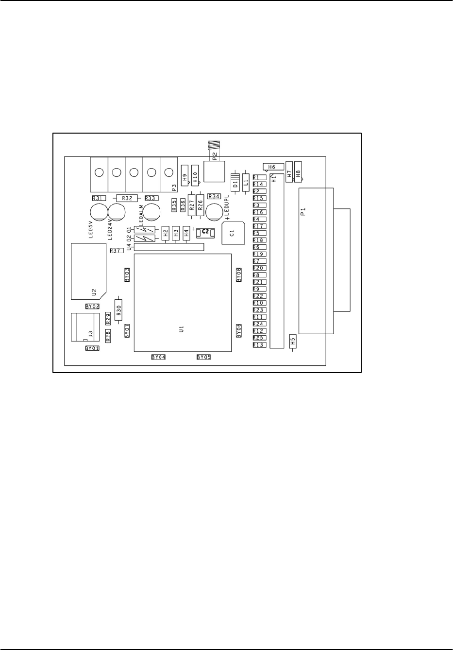
The DAFC is a small self-contained circuit board which can passively “eavesdrop” on the
RVP8’s serial uplink transmissions. Its purpose is to generate a set of digital AFC control lines
that could be applied, for example, to a custom STALO frequency synthesizer. A full size
(3”x3.75”) assembly diagram of the board is shown in Figure 2–3. It can be installed in the
radar system either as a bare board, or packaged into a small metal enclosure.
Figure 2–3: Assembly Diagram of the DAFC
SIGMET recommends that the DAFC board be used in new system designs whenever AFC is
required, as it offers these advantages over other methods of frequency control:
1) The use of a digital frequency synthesizer is superior to using analog AFC because
the stability of a synthesized STALO can be made much greater than that of a tunable
cavity oscillator. Also, noise on the AFC control voltage directly contributes to phase
noise in the received weather targets in analog AFC systems, so cabling of the control
signal can become tricky.
2) The RVP8 Connector Panel can also be made to output 8–bit AFC (TTL or
RS422). However, this is not in general recommended because of the potential for
noise on the cable which is typically run >2m into a radar cabinet. Using the DAFC
module is preferable because the board can be physically located very close to the
STALO. The length of the control cable and its susceptibility to noise and ground
loops are therefore reduced. Also, the DAFC board can supply up to 24 output
control lines, rather than just eight.
The digital output lines are made available as TTL levels on a 25-pin female “D” connector
(P1). There are 130W resistors (R1–R25) in series with each output line to help protect the
board against momentary application of non-TTL voltages on its external pins. However, these
resistors do impose a restriction on the input line configuration of the receiving device. To

Hardware Installation
RVP8 User’s Manual
September 2005
2–31
assure a valid TTL low level of 0.6V max. requires that the STALO inputs be pulled up to +5
with nothing less than (approx.) 1.2KW. Put another way, the low level input current of the
receiving device should not exceed 4.5mA. Most STALOs that we have seen use 5-20KW
pull-up resistors, so this should not be a problem.
All twenty five pins of the “D” connector are wired identically on the DAFC board, i.e., each pin
connects to one end of a 2-pin jumper (2x25 header H1), the other end of which connects to a
Programmable Logic Device (PLD) chip. The PLD lines can be configured either as inputs or
outputs, and this single chip handles all of the decoding and driving needs for the entire board.
For each “D” connector pin that is to be used as an AFC output or Fault Status input, you should
install the corresponding jumper to connect that pin through to the PLD, or use a wirewrap wire
if the pin must go to a different PLD line. The “D” connector pin numbers are printed next to
each of the jumper locations. Because of the ordering of the pins in the connector housing,
jumpers 1 through 13 are interleaved with jumpers 14 through 25.
The uplink protocol that the board should be expecting is selected by jumpers H3 and H4, as
summarized in Table 2–10. The first three table entries describe three fixed mappings of the
traditional AFC-16 uplink format onto various pins of the 25-pin “D” connector. One of these
choices must be used whenever the DAFC is interfaced to an RVP8 system whose uplink uses
the older style 16-bit AFC uplink format. In this case you will have to make most or all of the
pin assignments using wirewrap wire to connect each bit to its corresponding pin. This will be
somewhat tedious, but hopefully one of the three formats will be a reasonable starting point for
doing the wiring. By far the most preferable solution, however, is to use the Pinmap uplink
protocol (available since Rev.19) which allows for complete software mapping of all 25 external
pins.
Table 2–10: DAFC Protocol Jumper Selections
H4 H3 Function
On On AFC-16 format, Bits<0:15> on Pins<1:16>, Fault input on Pin 25
On Off AFC-16 format, Bits<0:15> on Pins<25:10>, Fault input on Pin 3
Off On AFC-16 format, Bits<0:15> on Pins<18, 19, 6, 7, 21, 22, 23, 11, 10, 9, 20,
8, 12, 25, 13, 24>, Fault input on Pin 4
Off Off Pinmap format, software assignment of all pins
Ground, +5V, and +24V power supply pins on the “D” connector should be connected with
wirewrap wire to the nearby power and ground posts H6, H7, and H8. The PLD jumpers for
these power supply pins must not be installed. Two 3K/6K resistive terminators are also
available at H5 for pulling pins up to approximately +3.3V when that is appropriate. Unused
“D” connector pins should remain both unwired and not jumpered.
Warning: It is important that the jumpers only be installed for pins that carry
TTL inputs or outputs destined for the on-board PLD. The jumpers must be
removed for all power supply pins, and for unused and reserved pins of the
external device.

Hardware Installation
RVP8 User’s Manual
September 2005
2–32
The DAFC board runs off of a single +5V power supply which can be applied either from the
STALO through the “D” connector, or externally through the terminal block. There are also
provisions for supplying +24V (approx.) between the terminal block and the “D” connector,
which is handy for cabling power to a STALO that requires the second voltage. Two green
LEDs indicate the presence of +5V and +24V. Terminal block Pin #1 is +5V, Pin #2 is +24V,
and Pin#3 is Ground. Pin #1 is the one nearest the corner of the board.
There is an option for having a “Fault Status” input on the “D” connector of the DAFC. Since
the board is completely passive in its connection to the uplink, the fault status bit will not affect
the uplink in any way. Rather, the bit is simply received by the board (with optional polarity
reversal) and driven onto the terminal block (P3) from whence it can be wired to some other
device, e.g., a BITE input line of an RCP02. A yellow LED is included to indicate the presence
of any external fault conditions.
The “AB” position of the 3-pin “Alarm” jumper (H9) connects the Fault Status signal to Pin #4
of the terminal block, whereas the “BC” position grounds that terminal block pin. A second
ground can be made available at Pin #5 of the terminal block by installing a jumper in the “BC”
position of the “Spare” 3-pin jumper (H10). This second ground could be used as a ground
return when the Fault Status line is driven off of the terminal block. The “AB” position of the
“Spare” jumper is reserved for some future input or output line on the terminal block.
Both the shield and the center conductor of the uplink SMA input connector (P2) are electrically
isolated (> 100KW) from the rest of the DAFC board. Moreover, the SMA connector pins
themselves are high-impedance and unterminated. What this means is that the board can be teed
into the uplink cable anywhere in the cable run from the RVP8/Rx board to the IFD. Since the
cable is driven by the RVP8/Rx, it must be at one end of the cable; and since termination is
provided by the IFD, it must be at the other end. The DAFC can be anywhere in the middle. Be
sure, however, that the TEE is located right at the DAFC itself so that an unterminated cable stub
is not created. A red LED is included to indicate that a valid uplink data stream is being
received.
A crystal oscillator is used to supply the operating clock for the on-board logic, and there are
two choices of frequency to use. If jumper H2 is “Off” then the crystal frequency should be
equal to the IFD’s sampling clock faq, and if H2 is “On” the frequency should be (0.75 faq).
Additional information about using AFC can be found in Sections 2.2.11, 3.2.6, and 5.1.3.
2.4.1 Example Hookup to a CTI “MVSR-xxx” STALO
Here is a complete example of what would need to be done in hardware and software to interface
the DAFC to a Communication Techniques Inc. digital STALO. The electrical interface for the
STALO is via a 26-pin ribbon cable which carries both Control and Status, as well as DC power.
This cable can be crimped onto a mass-terminated 25-pin “D” connector (with one wire
removed) and plugged directly into the DAFC. The resulting pinout is shown in Table 2–11.
The STALO frequency is controlled by a 14-bit binary integer whose LSB has a weight of 100
KiloHertz. In addition, the “Inhb” pin must be low for the STALO to function. Power is
supplied on the +5V and +24V pins, and two grounds are provided. An “alarm” output is also
available.

Hardware Installation
RVP8 User’s Manual
September 2005
2–33
Table 2–11: Pinout for the CTI “MVSR-xxx” STALO
Ribbon Pin “D” Pin Function Ribbon Pin “D” Pin Function
1 1 Ground 2 14 ––
3 2 +5V 4 15 ––
5 3 +24V 6 16 ––
7 4 Alarm 8 17 ––
9 5 –– 10 18 Bit–0
11 6 Bit–2 12 19 Bit–1
13 7 Bit–3 14 20 Bit–10
15 8 Bit–11 16 21 Bit–4
17 9 Bit–9 18 22 Bit–5
19 10 Bit–8 20 23 Bit–6
21 11 Bit–7 22 24 Ground
23 12 Bit–12 24 25 Bit–13
25 13 Inhb 26 –– ––
First configure the IFD pins themselves. Pins 1 and 24 are power supply grounds, and are
connected with wirewrap wire to the nearby ground posts. Pins 2 and 3 supply +5V and +24V
to the STALO, and should be wire wrapped to the internal power posts. The STALO power, as
well as the DAFC power, is then supplied externally via the terminal block on the DAFC itself.
Sixteen jumpers should be installed to connect the Control and Status lines, i.e., pins 4, 6–13,
18–23, and 25. We will use pinmap uplink protocol, so H3 and H4 are removed; and a x1
on-board crystal, so H2 is also removed.
The STALO has an output frequency range from 5200–6020MHz in 100KHz steps. In this
example we will assume that we need an AFC frequency span of 5580–5600MHz. This can be
done with the following setups from the Mb section:
AFC span– [–100%,+100%] maps into [ 3800 , 4000 ]
AFC format– 0:Bin, 1:BCD, 2:8B4D: 0, ActLow: NO
AFC uplink protocol– 0:Off, 1:Normal, 2:PinMap : 2
PinMap Table (Type ’31’ for GND, ’30’ for +5)
–––––––––––––––––––––––––––––––––––––––––––––
Pin01:GND Pin02:GND Pin03:GND Pin04:GND Pin05:GND
Pin06:02 Pin07:03 Pin08:11 Pin09:09 Pin10:08
Pin11:07 Pin12:12 Pin13:GND Pin14:GND Pin15:GND
Pin16:GND Pin17:GND Pin18:00 Pin19:01 Pin20:10
Pin21:04 Pin22:05 Pin23:06 Pin24:GND Pin25:13
FAULT status pin (0:None): 4, ActLow: NO
We map the AFC interval into the numeric span 3800–4000, and choose the “Bin” (simple
binary) encoding format. The actual frequency limits therefore match the desired values:
5200MHz + ( 3800 x 100KHz ) = 5580MHz
5200MHz + (4000 x 100KHz ) = 5600MHz
The “Inhb” line is held low, and fault status is input on Pin 4. Note that all pins that are not
directly controlled by the software uplink (e.g., power pins, and unused pins) are merely set to
“GND” in the setup table.

Hardware Installation
RVP8 User’s Manual
September 2005
2–34
2.4.2 Example Hookup to a MITEQ “MFS-xxx” STALO
The electrical interface for this STALO uses a 25-pin “D” connector with the following pin
assignments
SGROUND on pins 1 and 2.
SFour BCD digits of 1KHz, 10KHz, 100KHz, and 1MHz frequency steps, using Pins
<25:22>, <21:18>, <17:14>, <13:10>.
SSeven binary bits of representing 10MHz steps, Bits<0:6> on Pins<9:3>.
First configure the IFD pins themselves. Pins 1 and 2 are ground, and are connected with
wirewrap wire to the nearby ground posts. Pins 3 through 25 all are signal pins, so we plug in a
jumper for each of these 23 pins. We will use pinmap uplink protocol, so H3 and H4 are
removed; and a x1 on-board crystal, so H2 is also removed.
In this example we will assume that we wish to control the STALO in 20KHz steps from
1.350GHz to 1.365GHz. This can be done with the following setups from the Mb section:
AFC span– [–100%,+100%] maps into [ 1350000 , 1365000 ]
AFC format– 0:Bin, 1:BCD, 2:8B4D: 2, ActLow: NO
AFC uplink protocol– 0:Off, 1:Normal, 2:PinMap : 2
PinMap Table (Type ’31’ for GND, ’30’ for +5)
–––––––––––––––––––––––––––––––––––––––––––––
Pin01:GND Pin02:GND Pin03:22 Pin04:21 Pin05:20
Pin06:19 Pin07:18 Pin08:17 Pin09:16 Pin10:15
Pin11:14 Pin12:13 Pin13:12 Pin14:11 Pin15:10
Pin16:09 Pin17:08 Pin18:07 Pin19:06 Pin20:05
Pin21:GND Pin22:GND Pin23:GND Pin24:GND Pin25:GND
FAULT status pin (0:None): 0, ActLow: NO
We map the AFC interval into a numeric span from 1350000 to 1365000, and choose the
“8B4D” mixed-radix encoding format. The STALO itself has 1KHz frequency steps, but the
AFC servo will be easier to tune if we intentionally degrade this to 20KHz. This is done simply
by grounding all four of the 1KHz BCD input lines, plus the LSB of the 10KHz BCD digit. A
more creative use for one of these unused pins would be to remove the pin 25 jumper, wirewrap
pin 25 to ground (so the STALO sill reads it a logic low), and assign pin 25 as a fault status
input. That pin could then be connected to an external fault line, if the STALO has one.
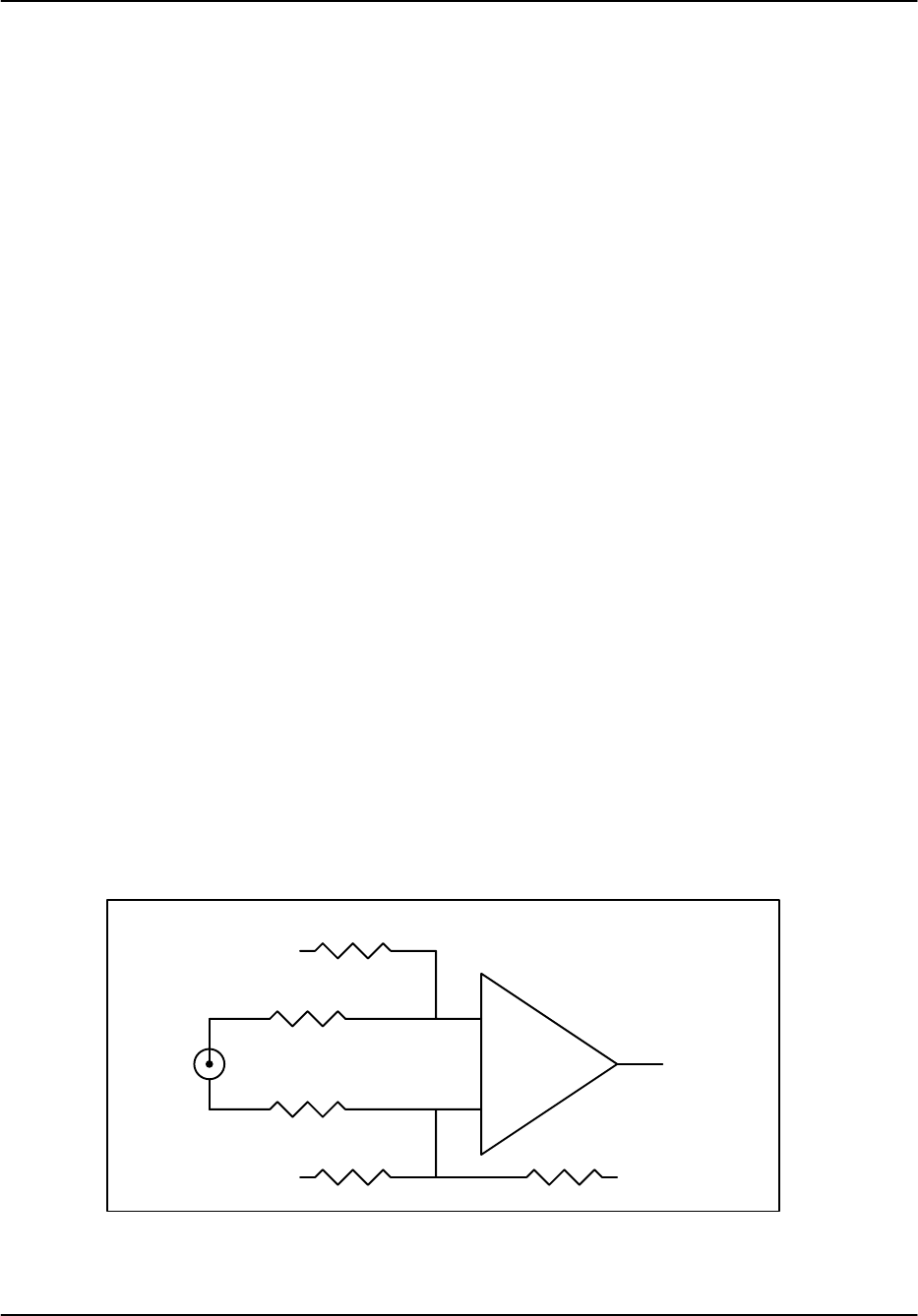
Hardware Installation
RVP8 User’s Manual
September 2005
2–35
2.5 RVP8 Custom Interfaces
This section describes some additional points of interface to the RVP8. These hookups are less
conventional than the “standard” interfaces described earlier in this chapter, but they sometimes
can supply exactly what is needed in exactly the right place. For the most part, these custom
interfaces are merely taps into existing internal signals that would normally not be seen by the
user.
2.5.1 Using the Legacy IFD Coax “Uplink”
In the previous RVP7 processor the Coax Uplink was the IFD’s single line of communication
from the main processor board. All of the information that was needed by the IFD would arrive
through this uplink; and as such, it contained information that might also be useful for other
parts of the radar system. In particular, it is a convenient source of digital AFC.
The RVP8 uses a single CAT-5E Uplink/Downlink cable between the IFD and RVP8/Rx PCI
card. The legacy coax uplink protocol is no longer used directly; but to help with backward
compatibility, the waveform is now synthesized as an output from the IFD. Any hardware that
used to be attached to the RVP7 coax uplink can still be driven from this new IFD port.
The uplink is a single digital transmission line that carries a hybrid serial protocol. The two
logic states, “zero” and “one” are represented by 0-Volt and +12-Volt (open circuit) electrical
levels. The output impedance of the uplink driver is approximately 55Ω. When the cable is
terminated in 75Ω the overall positive voltage swing will be approximately 8.6-Volts.
The electrical characteristics of the uplink have been optimized for balanced “groundless”
reception. The recommended eavesdropping circuit is shown in Figure 2–4, and consists of a
high speed comparator (Maxim MAX913, or equivalent) and input conditioning resistors. Both
the shield and the center conductor of the coax uplink feed the comparator through 33KΩ
isolation resistors; no direct ground attachment is made to the shield itself. The 500Ω resistors
provide the local ground reference, and the 47KΩ resistor supplies a bias to shift the unipolar
uplink signal into a bipolar range for the comparator.
Figure 2–4: Recommended Receiving Circuit for the Coax Uplink
Max913
or equiv.
33KW
33KW
500W
500W
47KW
Received
TTL
Signal
+5V
GND
GND
Coax
Uplink
Input
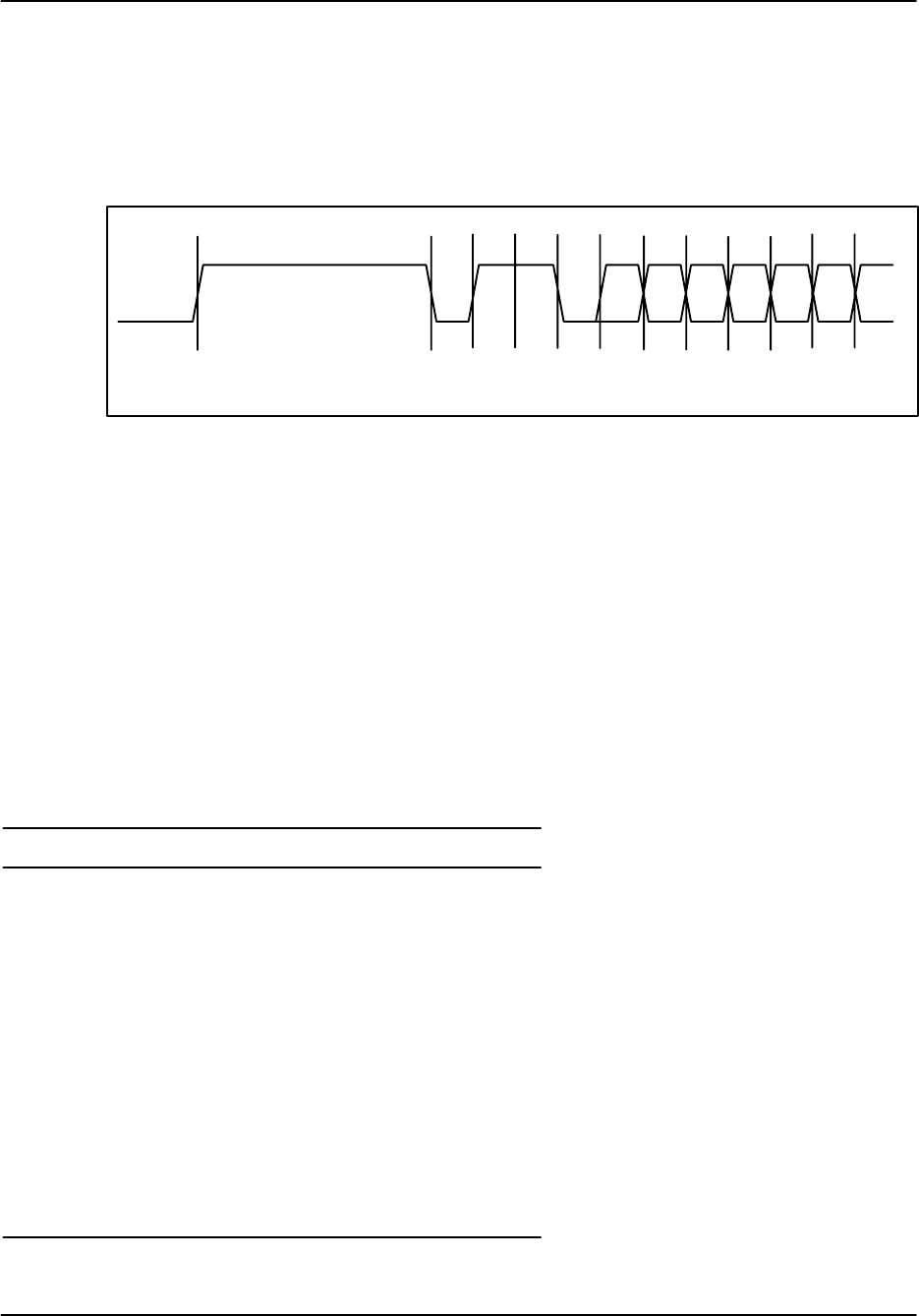
Hardware Installation
RVP8 User’s Manual
September 2005
2–36
The uplink signal, shown in Figure 2–5, is periodic at the radar pulse repetition frequency, and
conveys two distinct types of information to the IFD. The signal is normally low most of the
time (to minimize driver and termination power), but begins a transition sequence at the
beginning of each transmitted pulse.
Figure 2–5: Timing Diagram of the IFD Coax Uplink
12 345678910...
tburst tststststs
The first part of each pulse sequence is a variable length “burst window” which is centered on
the transmitted pulse itself, and which has a duration tburst approximately 800ns greater than the
length of the current FIR matched filter. The burst window defines the interval of time during
which the IFD transmits digitized burst pulse samples, rather than digitized IF samples, on its
downlink. The exact placement and width of the burst window will depend on the trigger timing
and digital filter specifications that the user has chosen, usually via the Pb and Ps plotting setup
commands.
Following the burst window is a fixed-length sequence of 25 serial data bits which convey
information from the RVP8/Rx board. The first four data bits form a characteristic (0,1,1,0)
marker pattern. The first zero in this pattern effectively marks the end of the variable length
burst window, and the other three bits should be checked for added confidence that a valid bit
sequence is being received. Table 2–12 defines the interpretation of the serial data bits.
Table 2–12: Bit Assignments for the IFD Coax Uplink
Bit(s) Meaning
1–4 Marker Sequence (0,1,1,0). This fixed 4-bit sequence identifies the start
of a valid data sequence following the variable-length burst window.
5–20 16-bit multi-purpose data word, MSB is transmitted first (See below)
21 Reset Request. This bit will be set in just one transmitted sequence
whenever an RVP8 reset occurs.
22 If set, then interpret the 16-bit data word as 4-bits of command and
12-bits of data, rather than as a single 16-bit quantity (See below)
23–24 Diagnostic select bits. These are used by the RVP8 power-up diagnostic
routines; they will both be zero during normal operation.
25 Green LED Request; 0=Off, 1=On. The state of this bit normally
follows the “Downlink Detect” LED on the RVP8/Rx board.

Hardware Installation
RVP8 User’s Manual
September 2005
2–37
The period ts of the serial data is (128ńfaq), where faq is the acquisition clock frequency given
in the Mc section of the RVP8 setup menu. For the default clock frequency of 71.9502MHz, the
period of the serial data will be 1.779μsec. The logic that is receiving the serial data should first
locate the center of the first data bit at (0.5 ts) past the falling edge at the end of the burst
window. Subsequent data bits are then sampled at uniform ts intervals.
The actual data sampling rate can be in error by as much as one part in 75 while still maintaining
accurate reception. This is because the data sequence is only 25-bits long, and hence, the last
data bit would still be sampled within 1/3 bit time of its center. Having this flexibility makes
it easier to design the receiving logic. For example, if a 5MHz or 10MHz clock were available,
then sampling at 1.8μsec intervals (1:85 error) would be fine. Likewise, one could sample at
1.75μsec based on a 4MHz or 8MHz clock (1:61 error), but only if the first sample were moved
slightly ahead of center so that the sampling errors were equalized over the 25-bit span.
Interpreting the Serial 16-bit Data Word
The serial 16-bit data word has several different interpretations according to how the RVP8 has
been configured, and whether Bit #22 of the uplink stream is set or clear. The evolution of these
different formats has been in response to new features being added to the IFD (Section 2.2), and
the production of the DAFC Digital AFC Module (Section 2.4).
The original use of the uplink data word was simply to convey a 16-bit AFC level, generally for
use with a magnetron system. Bit #22 is clear in this case, and the word is interpreted as a linear
signed binary value. The use of this format is discouraged for new hardware designs, but it will
remain available to guarantee compatibility with older equipment.
15 14 13 12 11 10 9 8 7 6 5 4 3 2 1 0
| | | | | | | | | | | | | | | | |
| 16–Bit AFC Level | AFC–16
|_______________________________________________________________|
Level 0111111111111111 (most positive AFC voltage)
0000000000000000 (center AFC voltage)
1000000000000000 (most negative AFC voltage)
When the IFD is jumpered for phase locking to an external reference clock, then Bit #22 will be
clear and the data word conveys the PLL clock ratio, and the Positive/Negative deviation sign of
the Voltage Controlled Crystal Oscillator (VCXO). This format is commonly used with klystron
systems, especially when the RVP8 is locking to an external trigger.
15 14 13 12 11 10 9 8 7 6 5 4 3 2 1 0
| | | | | | | | | | | | | | | | |
| |Pos| Numerator – 1 | Denominator – 1 | PLL–16
|___|___|___________________________|___________________________|
Note that the AFC-16 and PLL-16 formats can never be interleaved for use at the same time,
since there would be no way to distinguish them at the receiving end.
Finally, an expanded format has been defined to handle all future requirements of the serial
uplink. Bit #22 is set in this case, and the data word is interpreted as a 4-bit command and 12-bit
data value. A total of 16x12=192 auxiliary data bits thus become available via sequential
transmission of one or more of these words. The CMD/DATA words can also be used along
with one of the AFC-16 or PLL-16 formats, since Bit #22 marks them differently.

Hardware Installation
RVP8 User’s Manual
September 2005
2–38
15 14 13 12 11 10 9 8 7 6 5 4 3 2 1 0
| | | | | | | | | | | | | | | | |
| Command | Data | CMD/DATA
|_______________|_______________________________________________|
Commands #1, #2, and #3 control the 25 output pin levels of the DAFC board. These
transmissions may be interspersed with the PLL-16 format in systems that require both clock
locking and AFC, e.g., a dual-receiver magnetron system using a digitally synthesized COHO.
Note that the entire 25-bits of pin information are transferred synchronously to the output pins
only when CMD=3 is received. This assures that momentary invalid patterns will not be
produced upon arrival of CMD=1 or CMD=2 when the output bits are changing.
CMD=1 Data<0> DAFC output pin 25
Data<6> Fault Input is active high
Data<11:7> Which pin to use for Fault Input (0:None)
CMD=2 Data<11:0> DAFC output pins 24 through 13
CMD=3 Data<11:0> DAFC output pins 12 through 1
These three digital AFC pinmap commands are recommended as a replacement for the original
AFC-16 format in all new hardware designs. If you only need 12-bits of linear AFC, then map
the AFC range into the –2048 to +2047 numeric span, and select binary coding format (See
Section 3.2.6); the 12-bit data with CMD=3 will then hold the required values. To get a full
16-bit value, use a –32768 to +32767 span and extract the full word from both CMD=2 and
CMD=3. Of course, other combinations of bit formats and number of bits (up to 25) are also
possible.
Command #4 is used to control some of the internal features of the IFD. Bits <4:0> configure
the on-board noise generator so that it adds a selectable amount of dither power to the A/D
converters. This noise is bandlimited using a 10-pole lowpass filter so that most of the energy is
within the 150KHz to 900KHz band, with negligible residual power above 1.4MHz. Each of the
five bits switch in additional noise power when they are set, with the upper bits making
successively greater contributions. Bits <6:5> permit the IF-Input and Burst-Input signals to be
reassigned on the downlink.
CMD=4 Data<4:0> Built-in noise generator level
IF-Input and Burst-Input selection
Data<6:5> 00 : Normal 01 : Swap IF/Burst
10 : Burst Always 11 : IF Always
Data<7> 0 : Normal 1: Swap Pri/Sec IF
Data<8> Downlink IF data stream format
0 : Normal 72MHz single channel
1 : Half-band 36MHz dual channel
Data<9> 0 : Low Half-band 1: High Half-band