Baron Services DSSR-250C Pulsar Digital Solid-State Radar System User Manual
Baron Services Inc Pulsar Digital Solid-State Radar System
UserManual.wiki
>
Baron Services
>
DSSR-250C User Manual
>
Hardware Installation
Contents
1.
Users Manaul Cover Page and Table of Contents
2.
Hardware Limited Warranty
3.
Introduction and Specifications
4.
Hardware Installation
5.
Plot Assisted Setups
6.
Processing Algorithms
7.
TTY Nonvolatile Setups
8.
Host Computer Commands
Hardware Installation
Navigation menu
Upload a User Manual
Namespaces
Wiki Guide
HTML
PDF
Info
Views
User Manual
Discussion / Help
Navigation
![Hardware InstallationRVP8 User’s ManualSeptember 20052–14When two amplifiers are cascaded so that the output of the first drives the input of the second,the overall gain is the product of the two linear gains G1lin and G2lin, and the overall noise figure iscomputed from the two noise factors F1lin and F2lin as:NoiseFigure +10 log10ƪF1lin )ǒF2lin *1G1lin Ǔƫwhere the two noise factors are simply the linear representations of the noise figures that wereexpressed in deciBels:NoiseFigure +10 log10[NoiseFactor ] .Suppose that our first amplifier is an LNA/Preamp with a 2dB noise figure (noise factor 1.58),and we want to know what gain it must have such that, when cascaded into the RVP8/IFD, theoverall noise figure will be 3dB. The 32dB noise figure of the IFD is equivalent to a noisefactor of 1585, hence we have:3dB +10 log10ƪ1.58 )ǒ1585 *1G1lin Ǔƫfrom which we solve G1lin +3771, i.e., 35.8dB. This agrees with the 36dB of gain that wascomputed in the example of the previous section for the same RF/IF components and desiredoverall performance.2.2.10 Choice of Intermediate FrequencyThe RVP8 does not assume any particular relationship between the A/D sample clock and thereceiver’s intermediate frequency. You may operate at any IF that is at least 2MHz away fromany multiple of half the 35.9751MHz sampling rate (nominally 18, 36, 54, 72 MHz). The validfrequency bands are thus:6-16MHz, 20-34 MHz, 38-52 MHz, 56-70 MHzThere are many reasons for staying clear of the Nyquist frequency multiples. Most of theseconsiderations would apply to all types of digital processors, and are not specific to the RVP8.As an example of what can go wrong at the Nyquist frequencies, suppose that an intermediatefrequency of 35MHz was used. This is only 1MHz away from the (approximately) 36MHzsampling rate. The external anti-alias filter must now be designed much more carefully since aspurious input signal at 37MHz would be aliased into the valid 35MHz band. If the valid signalbandwidth were 2MHz, then the anti-alias filter would have the difficult task of passing34–36MHz free of distortion while rejecting everything above 36MHz. The filter’s transitionzone would have to be very sharp, and this is difficult to achieve.Another problem that would arise with a 35MHz IF on a magnetron system would be the RVP8’scomputation of AFC. If the processor can not distinguish 37MHz from 35MHz, then it can nottell the difference between the STALO being correctly on frequency, versus being 2MHz toohigh. The symmetric AFC tracking range would be reduced to the very small interval34–36MHz.](https://usermanual.wiki/Baron-Services/DSSR-250C.Hardware-Installation/User-Guide-669119-Page-14.png)
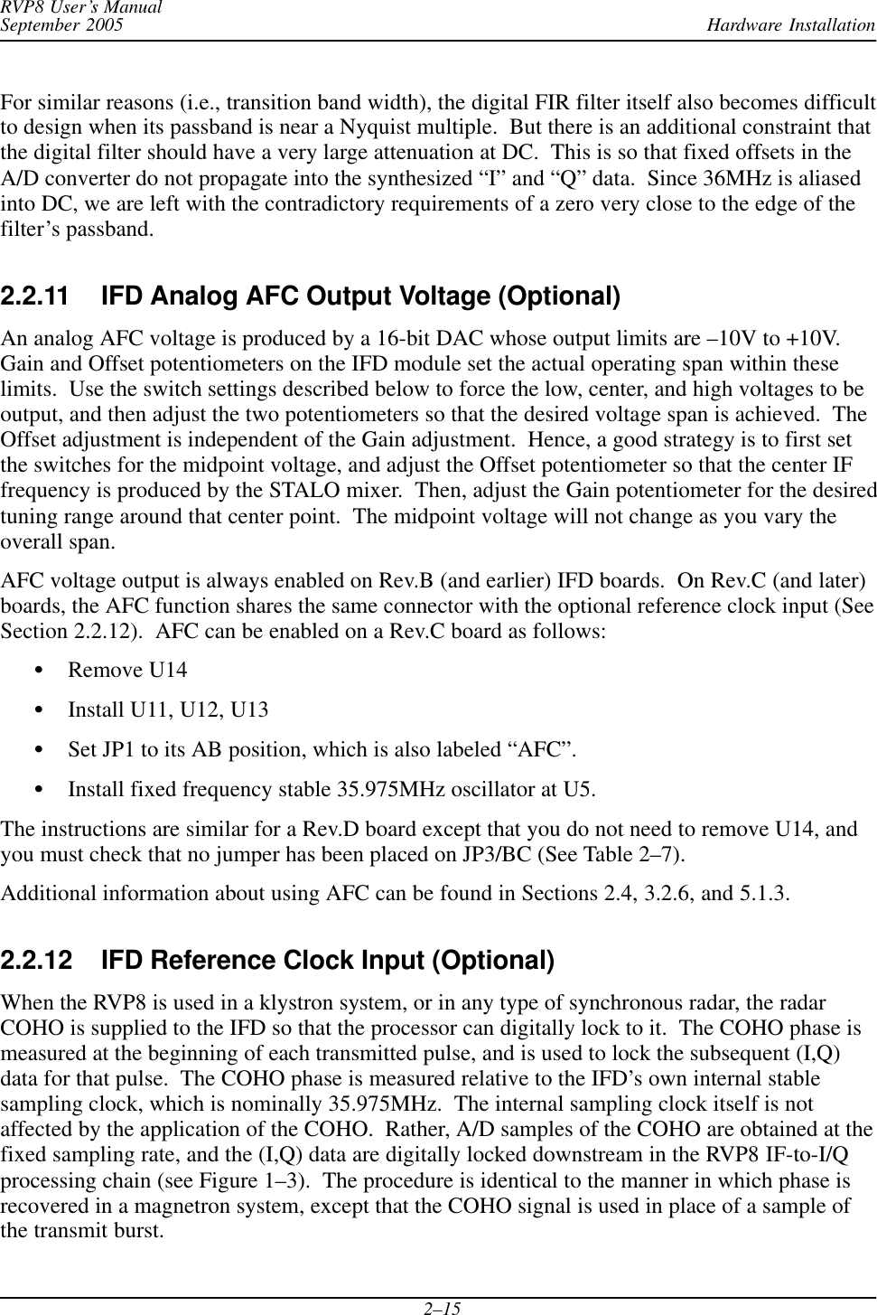
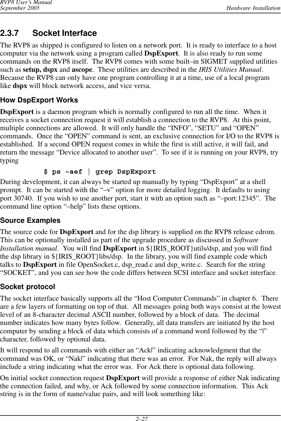
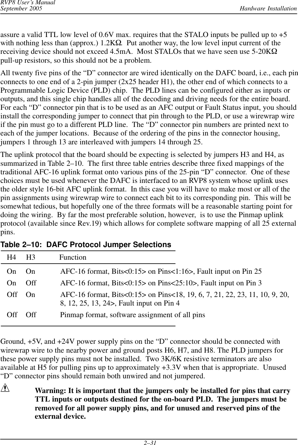
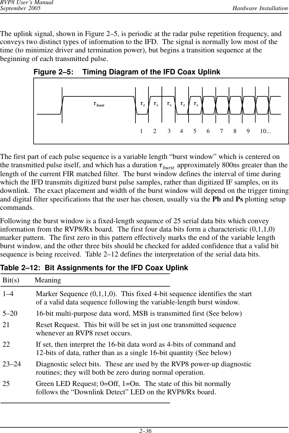
![Hardware InstallationRVP8 User’s ManualSeptember 20052–33Table 2–11: Pinout for the CTI “MVSR-xxx” STALO Ribbon Pin “D” Pin Function Ribbon Pin “D” Pin Function 1 1 Ground 2 14 –– 3 2 +5V 4 15 –– 5 3 +24V 6 16 –– 7 4 Alarm 8 17 –– 9 5 –– 10 18 Bit–0 11 6 Bit–2 12 19 Bit–1 13 7 Bit–3 14 20 Bit–10 15 8 Bit–11 16 21 Bit–4 17 9 Bit–9 18 22 Bit–5 19 10 Bit–8 20 23 Bit–6 21 11 Bit–7 22 24 Ground 23 12 Bit–12 24 25 Bit–13 25 13 Inhb 26 –– ––First configure the IFD pins themselves. Pins 1 and 24 are power supply grounds, and areconnected with wirewrap wire to the nearby ground posts. Pins 2 and 3 supply +5V and +24Vto the STALO, and should be wire wrapped to the internal power posts. The STALO power, aswell as the DAFC power, is then supplied externally via the terminal block on the DAFC itself.Sixteen jumpers should be installed to connect the Control and Status lines, i.e., pins 4, 6–13,18–23, and 25. We will use pinmap uplink protocol, so H3 and H4 are removed; and a x1on-board crystal, so H2 is also removed.The STALO has an output frequency range from 5200–6020MHz in 100KHz steps. In thisexample we will assume that we need an AFC frequency span of 5580–5600MHz. This can bedone with the following setups from the Mb section: AFC span– [–100%,+100%] maps into [ 3800 , 4000 ] AFC format– 0:Bin, 1:BCD, 2:8B4D: 0, ActLow: NO AFC uplink protocol– 0:Off, 1:Normal, 2:PinMap : 2 PinMap Table (Type ’31’ for GND, ’30’ for +5) ––––––––––––––––––––––––––––––––––––––––––––– Pin01:GND Pin02:GND Pin03:GND Pin04:GND Pin05:GND Pin06:02 Pin07:03 Pin08:11 Pin09:09 Pin10:08 Pin11:07 Pin12:12 Pin13:GND Pin14:GND Pin15:GND Pin16:GND Pin17:GND Pin18:00 Pin19:01 Pin20:10 Pin21:04 Pin22:05 Pin23:06 Pin24:GND Pin25:13 FAULT status pin (0:None): 4, ActLow: NOWe map the AFC interval into the numeric span 3800–4000, and choose the “Bin” (simplebinary) encoding format. The actual frequency limits therefore match the desired values:5200MHz + ( 3800 x 100KHz ) = 5580MHz5200MHz + (4000 x 100KHz ) = 5600MHzThe “Inhb” line is held low, and fault status is input on Pin 4. Note that all pins that are notdirectly controlled by the software uplink (e.g., power pins, and unused pins) are merely set to“GND” in the setup table.](https://usermanual.wiki/Baron-Services/DSSR-250C.Hardware-Installation/User-Guide-669119-Page-33.png)
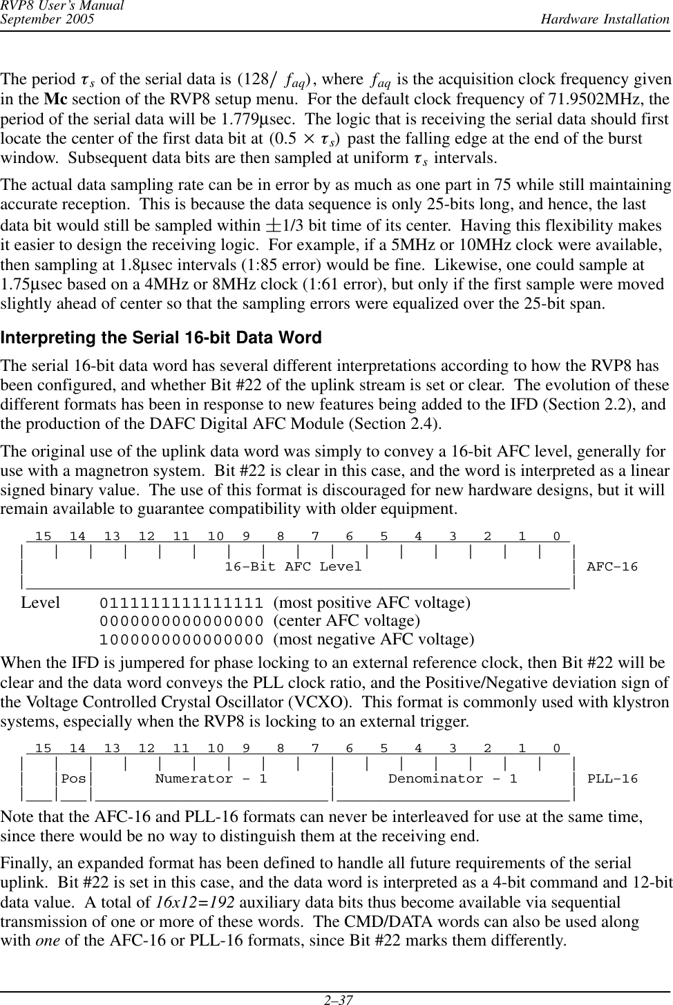
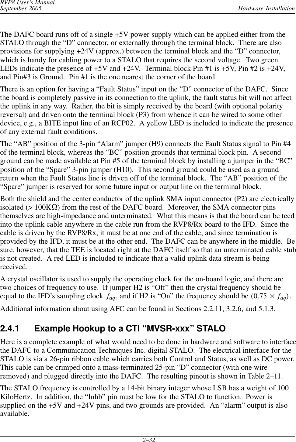
![Hardware InstallationRVP8 User’s ManualSeptember 20052–342.4.2 Example Hookup to a MITEQ “MFS-xxx” STALO The electrical interface for this STALO uses a 25-pin “D” connector with the following pinassignmentsSGROUND on pins 1 and 2.SFour BCD digits of 1KHz, 10KHz, 100KHz, and 1MHz frequency steps, using Pins<25:22>, <21:18>, <17:14>, <13:10>.SSeven binary bits of representing 10MHz steps, Bits<0:6> on Pins<9:3>.First configure the IFD pins themselves. Pins 1 and 2 are ground, and are connected withwirewrap wire to the nearby ground posts. Pins 3 through 25 all are signal pins, so we plug in ajumper for each of these 23 pins. We will use pinmap uplink protocol, so H3 and H4 areremoved; and a x1 on-board crystal, so H2 is also removed.In this example we will assume that we wish to control the STALO in 20KHz steps from1.350GHz to 1.365GHz. This can be done with the following setups from the Mb section: AFC span– [–100%,+100%] maps into [ 1350000 , 1365000 ] AFC format– 0:Bin, 1:BCD, 2:8B4D: 2, ActLow: NO AFC uplink protocol– 0:Off, 1:Normal, 2:PinMap : 2 PinMap Table (Type ’31’ for GND, ’30’ for +5) ––––––––––––––––––––––––––––––––––––––––––––– Pin01:GND Pin02:GND Pin03:22 Pin04:21 Pin05:20 Pin06:19 Pin07:18 Pin08:17 Pin09:16 Pin10:15 Pin11:14 Pin12:13 Pin13:12 Pin14:11 Pin15:10 Pin16:09 Pin17:08 Pin18:07 Pin19:06 Pin20:05 Pin21:GND Pin22:GND Pin23:GND Pin24:GND Pin25:GND FAULT status pin (0:None): 0, ActLow: NOWe map the AFC interval into a numeric span from 1350000 to 1365000, and choose the“8B4D” mixed-radix encoding format. The STALO itself has 1KHz frequency steps, but theAFC servo will be easier to tune if we intentionally degrade this to 20KHz. This is done simplyby grounding all four of the 1KHz BCD input lines, plus the LSB of the 10KHz BCD digit. Amore creative use for one of these unused pins would be to remove the pin 25 jumper, wirewrappin 25 to ground (so the STALO sill reads it a logic low), and assign pin 25 as a fault statusinput. That pin could then be connected to an external fault line, if the STALO has one.](https://usermanual.wiki/Baron-Services/DSSR-250C.Hardware-Installation/User-Guide-669119-Page-34.png)