CAEN RFID srl CAENRFID010 Low Power OEM UHF Compact RFID Reader User Manual CAENRFIDLibrary
CAEN RFID srl Low Power OEM UHF Compact RFID Reader CAENRFIDLibrary
Contents
- 1. Users Manual I
- 2. Users Manual II
- 3. Users Manual III
- 4. Users Manual IV
- 5. User Manual
Users Manual III
R1230CB
OEM UHF Multiregional Ultra Compact Reader
R1230CBEVB
Quark Reader Evaluation Board
R1230ADAT
Quark Adapter Board
Technical Information Manual
Revision n. 00
25/11/2010

Scope of Manual
The goal of this manual is to provide the basic information to work with the QUARK family.
Change Document Record
Date
Revision
Changes
25 Nov 2010
00
Preliminary release.
CAEN RFID srl
Via Vetraia, 11 55049 Viareggio (LU) - ITALY
Tel. +39.0584.388.398 Fax +39.0584.388.959
info@caenrfid.it
www.caenrfid.it
© CAEN RFID srl – 2010
Disclaimer
No part of this manual may be reproduced in any form or by any means, electronic, mechanical, recording, or
otherwise, without the prior written permission of CAEN RFID.
The information contained herein has been carefully checked and is believed to be accurate; however, no responsibility
is assumed for inaccuracies. CAEN RFID reserves the right to modify its products specifications without giving any
notice; for up to date information please visit www.caenrfid.it.
Federal Communications Commission (FCC) Notice (Preliminary)
This device was tested and found to comply with the limits set forth in Part 15 of the FCC Rules. Operation is subject to
the following conditions: (1) this device may not cause harmful interference, and (2) this device must accept any
interference received including interference that may cause undesired operation. These limits are designed to provide
reasonable protection against harmful interference when the equipment is operated in a commercial environment.
This device generates, uses, and can radiate radio frequency energy. If not installed and used in accordance with the
instruction manual, the product may cause harmful interference to radio communications. Operation of this product in
a residential area is likely to cause harmful interference, in which case, the user is required to correct the interference
at their own expense. The authority to operate this product is conditioned by the requirements that no modifications
be made to the equipment unless the changes or modifications are expressly approved by CAEN RFID.
Preliminary Product Information
This document contains information for a new product. CAEN RFID reserves the right to modify this product without
notice.
“Preliminary” product information describes products that are ready for production, but for which full characterization
data is not yet available. CAEN RFID believes that the information contained in this document is accurate and reliable.
However, the information is subject to change without notice and is provided “AS IS” without warranty of any kind
(Express or implied). You are advised to obtain the latest version of relevant information to verify, before placing
orders, that information being relied on is current and complete. All products are sold subject to the terms and
conditions of sale supplied at the time of order acknowledgement, including those pertaining to warranty, patent
infringement, and limitation of liability. No responsibility is assumed by CAEN RFID for the use of this information,
including use of this information as the basis for manufacture or sale of any items, or for infringement of patents or
other rights of third parties.
Disposal of the product
Do not dispose the product in municipal or household waste. Please check your local regulations for
disposal/recycle of electronic products.
QUARK R1230CB - R1230BEVB - R1230ADAT - Technical Information Manual
3
Index
Scope of Manual .......................................................................................................................... 2
Change Document Record ........................................................................................................... 2
Index.......................................................................................................................................... 3
List of Figures ............................................................................................................................. 4
List of Tables .............................................................................................................................. 4
1 Introduction ....................................................................................................................... 5
General Information .................................................................................................................... 6
Ordering Code .............................................................................................................................. 7
Installation Notice ........................................................................................................................ 8
2 Quark R1230CB .................................................................................................................. 9
Technical Specifications Table ................................................................................................... 10
External Connections ................................................................................................................. 11
R1230CB supply and I/O connector electrical characteristics ......................................... 13
Power supply connection ................................................................................................. 14
General purpose I/O connections .................................................................................... 14
External reset ................................................................................................................... 15
UART connection .............................................................................................................. 15
Antenna port specifications ............................................................................................. 15
Reader – Tag Link Profiles .......................................................................................................... 16
Firmware Upgrade ..................................................................................................................... 16
BLS operation ................................................................................................................... 16
Firmware upgrade via R1230CBEVB board ...................................................................... 17
PCB Pad Layout .......................................................................................................................... 17
3 Quark R1230CBEVB .......................................................................................................... 18
Technical Specifications Table ................................................................................................... 19
Connection diagram .................................................................................................................. 19
Technical drawings .................................................................................................................... 20
Electrical scheme ....................................................................................................................... 21
External Connections ................................................................................................................. 22
4 Quark R1230ADAT ............................................................................................................ 23
Technical Specifications Table ................................................................................................... 24
Technical drawings .................................................................................................................... 24
Electrical scheme ....................................................................................................................... 25
External Connections ................................................................................................................. 26
5 Quark Regulatory Compliance .......................................................................................... 27
FCC Compliance ......................................................................................................................... 28

QUARK R1230CB - R1230BEVB - R1230ADAT - Technical Information Manual
4
List of Figures
Fig. 1.1: QUARK R1230CB OEM UHF Multiregional compact reader................................................... 6
Fig. 1.2: QUARK R1230CBEVB - Quark Reader Evaluation Board ........................................................ 6
Fig. 1.3: QUARK R1230ADAT - Quark Adapter Board .......................................................................... 6
Fig. 1.4: Connection of the R1230CBEVB to the Quark R1230CB module. .......................................... 8
Fig. 1.5: Connection of the R1230ADAT to the Quark R1230CB module. ........................................... 8
Fig. 2.1: QUARK R1230CB technical drawings: top view.................................................................... 11
Fig. 2.2: QUARK R1230CB technical drawings: lateral views ............................................................. 11
Fig. 2.3: QUARK R1230CB power supply connection ......................................................................... 14
Fig. 2.4: QUARK R1230CB GPIO connection example ........................................................................ 14
Fig. 2.5: QUARK R1230CB external reset ........................................................................................... 15
Fig. 2.6: QUARK R1230CB RS232 connection ..................................................................................... 15
Fig. 2.7: BSL sequence ........................................................................................................................ 16
Fig. 2.8: QUARK R1230CB upgrade program window ........................................................................ 17
Fig. 2.9: PCB pad layout ...................................................................................................................... 17
Fig. 3.1: Quark R1230CBEVB technical drawing ................................................................................. 20
Fig. 3.2: Quark R1230CBEVB electrical scheme ................................................................................. 21
Fig. 4.1: Quark R1230ADAT technical drawing .................................................................................. 24
Fig. 4.2: Quark R1230ADAT electrical scheme ................................................................................... 25
List of Tables
Tab. 2.1: QUARK R1230CB Technical Specifications .......................................................................... 10
Tab. 2.2: QUARK R1230CB connector pinout .................................................................................... 12
Tab. 2.3: QUARK R1230CB supply and I/O connector electrical characteristics ............................... 13
Tab. 2.4: RF port pinout ..................................................................................................................... 15
Tab. 2.5: RF port electrical characteristics ......................................................................................... 16
Tab. 2.6: QUARK R1230CB reader to tag link profiles........................................................................ 16
Tab. 3.1: QUARK R1230CBEVB Technical Specifications .................................................................... 19
Tab. 3.2: QUARK R1230CBEVB connector pinout .............................................................................. 22
Tab. 4.1: QUARK R1230ADAT Technical Specifications ..................................................................... 24
Tab. 4.2: QUARK R1230ADAT connector pinout ................................................................................ 26

QUARK R1230CB - R1230BEVB - R1230ADAT - Technical Information Manual
6
General Information
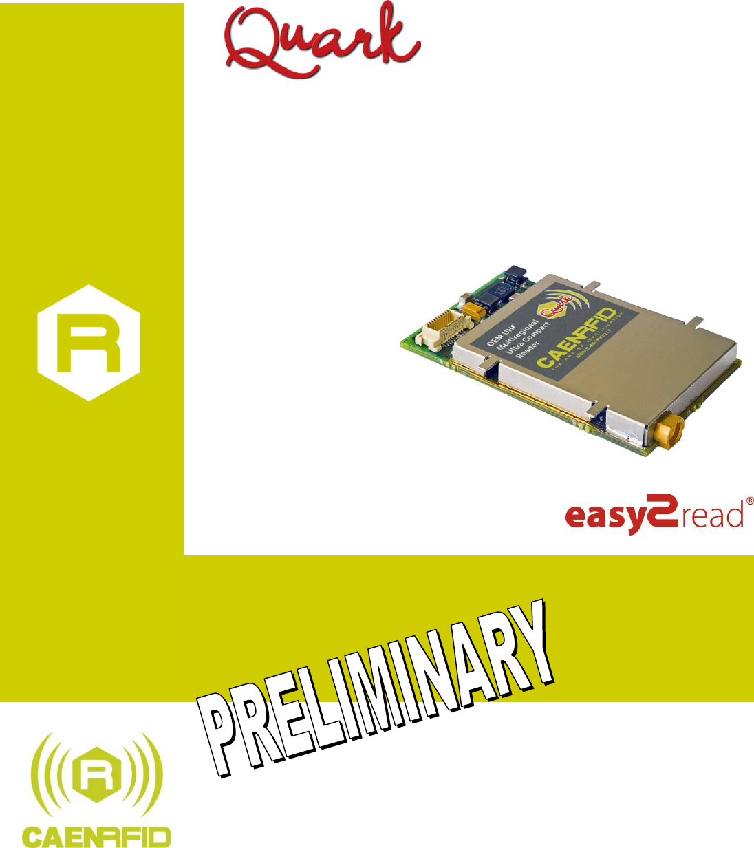
The Quark (Model R1230CB), the new OEM reader of the easy2read© Family, is an UHF multiregional ultra compact
reader for low-power, high performances UHF RFID applications.
With programmable output power in 15 steps from 9dBm to 23dBm, the reader can detect tags at more than 2 mt of
distance (depending on antenna and tag dimensions).
Due to its low power consumption, the module is specifically designed to be easily integrated in battery powered
devices as well as powered directly by a standard USB port.
The radio frequency core of the module permits to achieve fast reading and to be used in dense reader and dense tag
environments for top-class rated performances.
The compactness of the device and the board-to-board connector allow to embed the R1230CB inside the new small
form factor industrial handhelds, smartphone accessories, small USB dongles and other compact form factor devices.
The R1230CB complies with and can operate in both European and US regulatory environments and due to its
multiregional capabilities, it is ideal for integration in devices requiring compliance to different geographical regions.
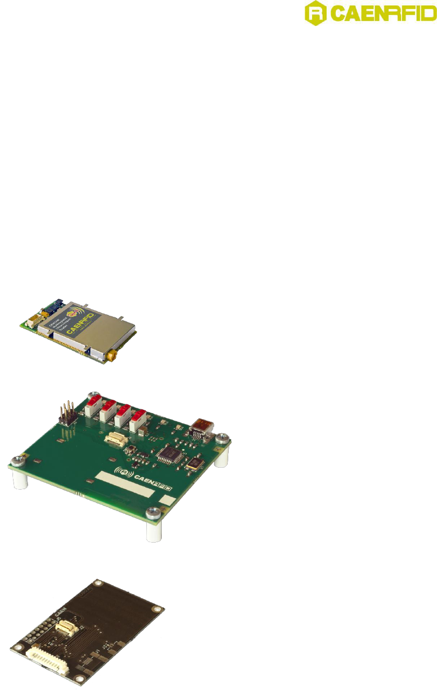
The Mod. R1230CBEVB evaluation board allows to manage the Mod. R1230CB OEM UHF multiregional Compact Reader
directly via USB
In case customers want to replace directly with Quark reader others CAEN RFID OEM modules (i.e. A828, A828A, A528),
the Mod. R1230ADAT adapter board can be used.
Fig. 1.1: QUARK R1230CB OEM UHF Multiregional compact reader
Fig. 1.2: QUARK R1230CBEVB - Quark Reader Evaluation Board
Fig. 1.3: QUARK R1230ADAT - Quark Adapter Board
QUARK R1230CB - R1230BEVB - R1230ADAT - Technical Information Manual
7
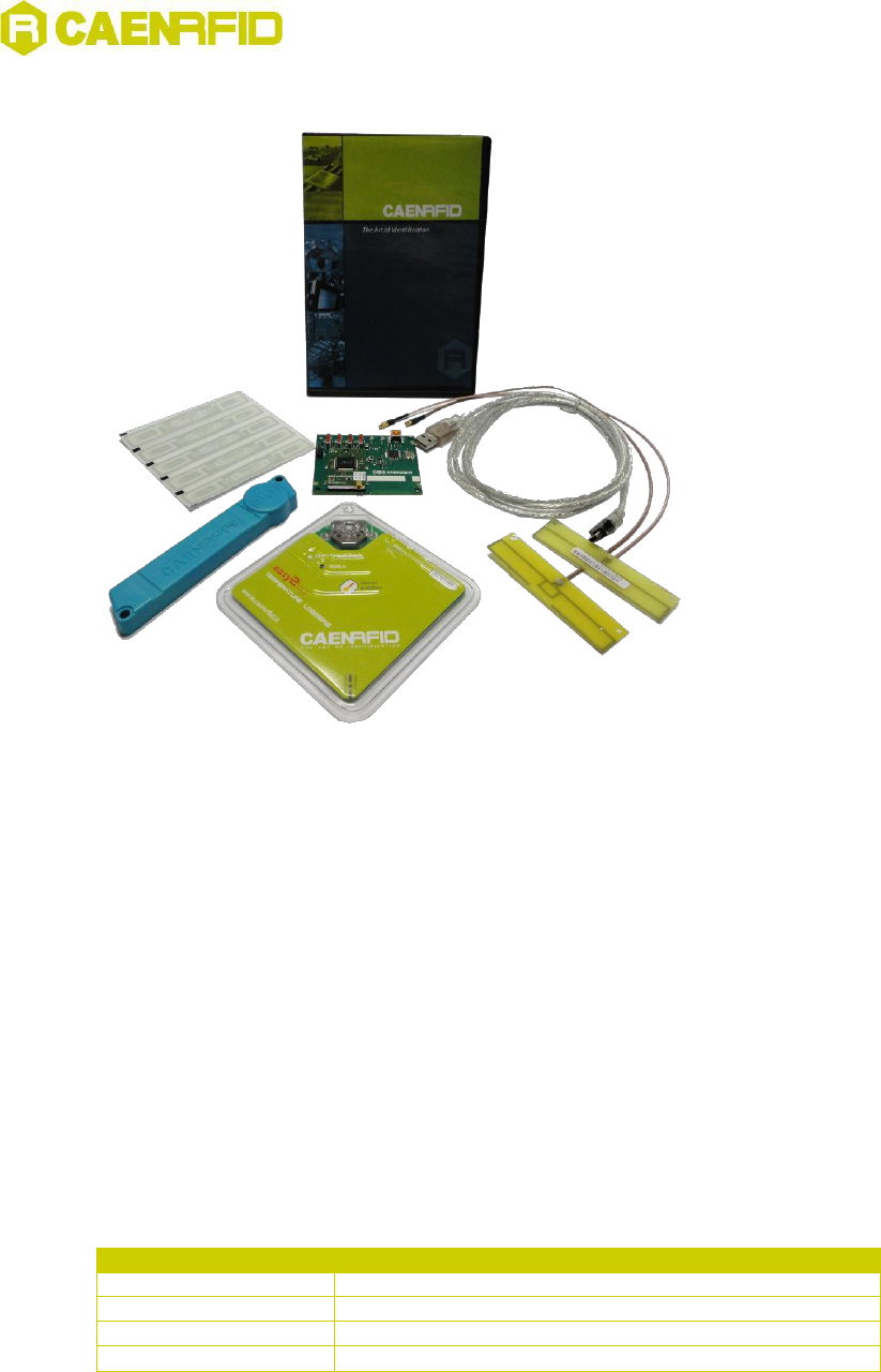
It is also available the R1230CBDK Development KIT with QUARK reader, antenna, tags.
Kit contents:
no. 1 R1230CB - Quark Low Power OEM UHF Compact RFID Reader
no. 1 R1230CBEVB - Quark Reader Evaluation Board
no. 5 WEPCLABEL002 - EPC C1G2 Label Short Dipole EU
no. 1 A927Z - Temperature logger UHF semi-passive tag (EPC C1G2)
no. 1 RT0005 - Temperature logger UHF semi-passive tag (EPC C1G2) Blistered
no. 1 WANTENNAX009 - Linear polarized antenna for printers 865 - 870 MHz (ETSI)
no. 1 WANTENNAX012 - Linear polarized antenna for printers 902 - 928 MHz (FCC)
no. 1 cable MINI USB - no. 1 CD-ROM containing SW libraries, CAENRFID demo SW and technical manuals
Ordering Code
Code
Description
WR1230ADAT01
R1230ADAT - Quark Adapter Board
WR1230CBEVBX
R1230CBEVB - Quark Reader Evaluation Board
WR1230CXBAAA
R1230CB – Quark Low Power OEM UHF Compact RFID Reader
WR1230CBDKEU
R1230CBDK - Development KIT with QUARK reader, antenna, tags
QUARK R1230CB - R1230BEVB - R1230ADAT - Technical Information Manual
8
Installation Notice
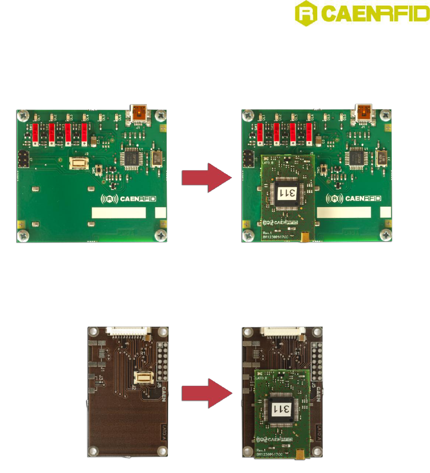
The correct way to connect the Quark R1230CB module to the evaluation board and the adapter board is shown in the
following pictures.
Fig. 1.4: Connection of the R1230CBEVB to the Quark R1230CB module.
Fig. 1.5: Connection of the R1230ADAT to the Quark R1230CB module.

QUARK R1230CB - R1230BEVB - R1230ADAT - Technical Information Manual
9
2 Quark R1230CB
This Chapter provide the basic information to work with the Quark R1230CB multiregional
ultra compact reader. It contains these topics:
Technical Specifications Table
External Connections
Reader – Tag Link Profiles
Firmware Upgrade
PCB Pad Layout

QUARK R1230CB - R1230BEVB - R1230ADAT - Technical Information Manual
10
Technical Specifications Table
Frequency Band
902÷928 MHz (FCC part 15)
865.600÷867.600 MHz (ETSI EN 302 208)
Output Power Level
Programmable in 15 levels (1dB step) from 9dBm to 23dBm (from 8mW to
200mW) conducted
Output Power Accuracy
+/- 1dB
Antenna VSWR Requirement
2:1 or better for optimum performances
Antenna Connector
Nr. 1 MMCX type
Frequency Tolerance
±10 ppm over the entire temperature range
Number of Channels
4 channels (compliant to ETSI EN 302 208 v1.2.1)
50 hopping channels (compliant to FCC part 15.247).
All subsets of 902-928 MHz band are supported
Standard Compliance
EPC C1G2
Others by FW upgrade
Digital I/O
Four I/O lines 3.3V out @ 3mA; 3.3V input level
UART Serial Port
Baudrate: 115200
Databits: 8
Stopbits: 1
Parity: none
Flow control: none
3.3 V I/O voltage level
9.6÷115 kbit/s data rate (settable)
Dimensions
(W)25 x (L)40 x (H)6 mm3
(1.0 x 1.6 x 0.2 inch3)
Supply Voltage Range
2.5V ÷ 5.5V
Power Consumption
- 1.6W @ RF out = 23dBm
- 1.3W @ RF out = 17dBm
- 0.25W in idle mode
Operating Temperature
-10 °C to +55 °C
Weight
8 g
Tab. 2.1: QUARK R1230CB Technical Specifications
QUARK R1230CB - R1230BEVB - R1230ADAT - Technical Information Manual
11
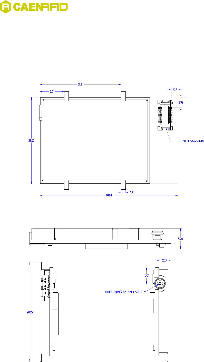
External Connections
The location of the connectors is shown in Fig. 2.1. Their mechanical specifications are listed below:
Antenna Port: RF Coax Connector Huber+Suhner type 82MMCX-S50-0-2/111_K (to be used with Huber+Suhner type
11MMCX-50-1-1/111_O).
Supply and I/O connector: Molex P.N. 53748-0208 (mates with Molex 52991-0208 to be used on the host board).
Fig. 2.1: QUARK R1230CB technical drawings: top view
Fig. 2.2: QUARK R1230CB technical drawings: lateral views

QUARK R1230CB - R1230BEVB - R1230ADAT - Technical Information Manual
12
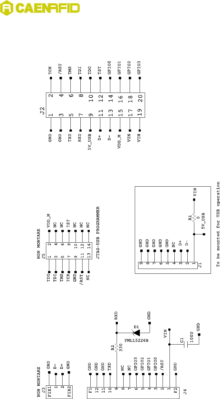
Supply and I/O connector pinout is shown in the following table1:
Pin #
Signal
Description
1
GND
Ground
2
TCK
TCK JTAG signal (debug purpose only)
3
GND
Ground
4
/RST
Reset (active low)
5
TXD
UART TX to host
6
TMS
TMS JTAG signal (debug purpose only)
7
RXD
UART RX from host
8
TDI
TDI JTAG signal (debug purpose only)
9
5V_OUT
5Vdc auxiliary output voltage
10
TDO
TDO JTAG signal (debug purpose only)
11
BSL_SEL
Bootloader interface selection2
12
TST
TST JTAG signal (also for BSL operation)
13
VDD_M
3.3Vdc auxiliary output voltage
14
GPIO0
General Purpose IO #0
15
VDD_M
3.3Vdc auxiliary output voltage
16
GPIO1
General Purpose IO #1
17
VIN
Input supply voltage
18
GPIO2
General Purpose IO #2
19
VIN
Input supply voltage
20
GPIO3
General Purpose IO #3
Tab. 2.2: QUARK R1230CB connector pinout
The GPIO0-GPIO3 pins are 4 general purpose bidirectional pins, their default direction (or after a Reset) is input.
The RXD/TXD pins are used to communicate with the Quark reader via UART port; to establish a link with the device
you must configure your COM port as follows:
Baud rate: 115200
Parity: None
Data bits: 8
Stop bits: 1
Flow Control: none
JTAG pins, unless otherwise noted, are for internal debug purpose only and shall not be connected by the user.
/RST, BSL_SEL and TST pins shall be properly driven to start the bootloader of R1230CB embedded microcontroller in
case the user wants to upgrade the firmware image of the reader. In normal operation BSL_SEL and TST shall be at low
level or left unconnected.
See § BLS operation (pag. 16) for the description of bootloader operation.
VDD_M and 5V_OUT are two auxiliary supply sources with 20mA maximum current capability to be used as supply
voltages of external components.
1 Debug purpose and unused pins should not be connected.
2 If BSL_SEL is at high level, the UART interface is connected to the serial port dedicated to microcontroller Boot Strap Loader operation required for
flashing the firmware inside the MCU memory. This pin shall be at low level or left unconnected in normal operation.

QUARK R1230CB - R1230BEVB - R1230ADAT - Technical Information Manual
13
R1230CB supply and I/O connector electrical characteristics3
Pin name
Pin No.
Parameter
Min
Type
Max
Unit
GND
1,3
TCK
2
VIL
-0.3
0.75
V
VIH
1.5
3.6
V
Input current
10
μA
/RESET
4
VIL
-0.3
0.6
V
VIH
1.65
3.6
V
Internal pull-up resistance
47
k
Ω
Pulse width
10
μs
TXD
5
VOL
0
0.55
V
VOH
2.5
3.5
V
Output current
3.0
mA
TMS
6
VIL
-0.3
0.75
V
VIH
1.5
3.6
V
Input current
10
μA
RXD
7
VIL
-0.3
0.75
V
VIH
1.5
3.6
V
Input current
10
μA
TDI
8
VIL
-0.3
0.75
V
VIH
1.5
3.6
V
Input current
10
μA
5V_OUT
9
Output DC voltage
4.75
5.00
5.25
V
Output current
20
mA
TDO
10
VOL
0
0.55
V
VOH
2.5
3.5
V
Output current
3.0
μA
BSL_SEL
11
VIL
-0.3
1.0
V
VIH
2.2
3.6
V
Internal pull-down resistance
10
kΩ
TST
12
VIL
-0.3
0.75
V
VIH
1.5
3.6
V
Internal pull-down resistance
45
kΩ
VDD_M
13,15
Output DC voltage
3.1
3.3
3.5
V
Output current
20
mA
GPIO[0:3]
14, 16,
18, 20
VOL
0
0.55
V
VOH
2.5
3.5
V
Output current
3.0
mA
VIL
-0.3
0.75
V
VIH
1.5
3.6
V
Input current
10
μA
VIN4
17,19
Input supply voltage
2.5
5.5
V
Supply current @ Vin = 2.5V
0.68
A
Supply current @ Vin = 3.7V
0.42
A
Supply current @ Vin = 5.0V
0.30
A
Tab. 2.3: QUARK R1230CB supply and I/O connector electrical characteristics
3 Exceeding maximum values reported in the table may cause permanent damage to the model.
4 External 100uF bypass capacitor between Vin and GND is recommended for proper operation.
QUARK R1230CB - R1230BEVB - R1230ADAT - Technical Information Manual
14
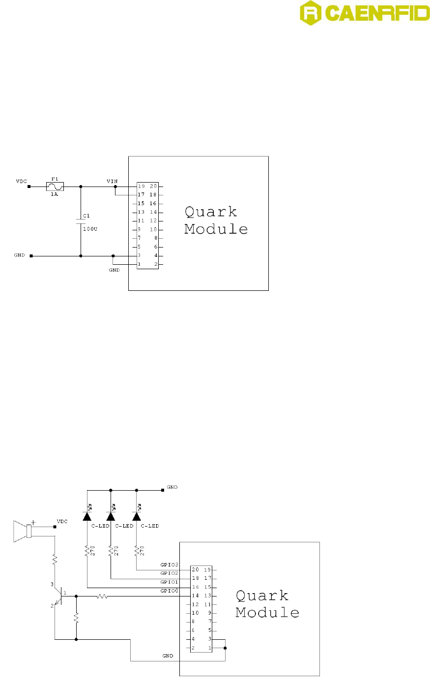
Power supply connection
In the following schematic suggested R1230CB power supply connection is shown.
An external 100uF bypass capacitor between Vin and GND is recommended for proper operation.
The use of fuse F1 (or an equivalent solid state current limiter) is recommended since R1230CB doesn't provide internal
current limitation protection.
Fig. 2.3: QUARK R1230CB power supply connection
General purpose I/O connections
The GPIO0-GPIO3 pins are 4 general-purpose bidirectional pins. Their default direction after a power on reset or a
general reset is set to input.
GPIO, when configured as Outputs, can be used to drive indicators as leds or buzzers or to send trigger signal to others
equipments.
GPIO, when configured as Inputs, can accept control signals from other equipments or trigger signals from sensors (i.e.
photocells).
In the following schematic an example of application of GPIO is shown.
Fig. 2.4: QUARK R1230CB GPIO connection example
QUARK R1230CB - R1230BEVB - R1230ADAT - Technical Information Manual
15
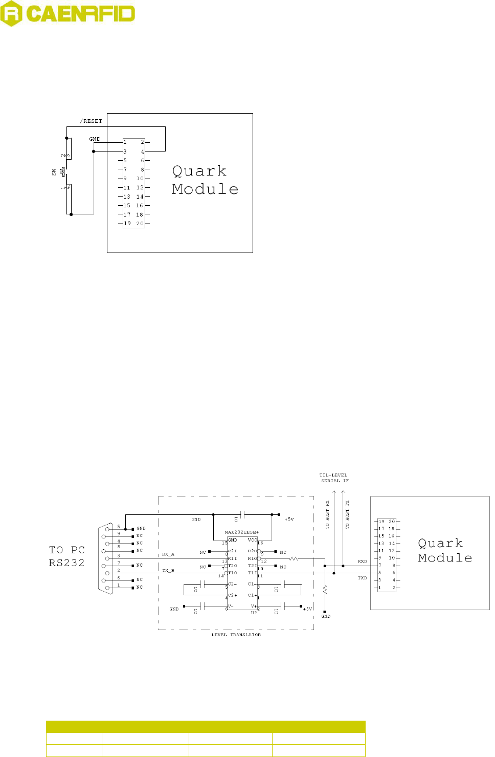
External reset
R1230CB manual reset can be performed by forcing at low level /RESET pin for 10μs at least. /RESET pin is pulled-up by
an internal resistor.
Fig. 2.5: QUARK R1230CB external reset
UART connection
The RXD/TXD pins are used to communicate with the R1230CB board via UART port. Since Quark RX/TX are TTL level
signals, in order to connect it with a PC, a TTL/RS232 translator shall be used (please refer to the diagram below).
To establish a link with the device host COM port shall be configured as follows:
Baud rate: 115200
Parity: None
Data bits: 8
Stop bits: 1
Flow Control: none
Fig. 2.6: QUARK R1230CB RS232 connection
Antenna port specifications
In the following table the pinout of R1230CB antenna is shown.
Pin #
Function
Direction
Description
INNER
RF OUT
OUT
RF output
OUTER
GND
-
Ground
Tab. 2.4: RF port pinout
QUARK R1230CB - R1230BEVB - R1230ADAT - Technical Information Manual
16
Parameter
Min
Typ.
Max
Unit
RF output power
8
200
mW
9
23
dBm
Output power vs. power setting accuracy
± 1
dB
RF port impedance
50
Ω
Recommended antenna VSWR
2:1
-
Tab. 2.5: RF port electrical characteristics
Reader – Tag Link Profiles
Quark reader supports different modulation and return link profiles according to EPC Class1 Gen2 protocol.
In the following table are reported all profiles that have been tested for the compliance with ETSI and FCC regulations.
Link profile #
Regulation
Modulation
Return Link
0
ETSI - FCC
DSB–ASK; f=40kHz
FM0; f = 40kHz
1
ETSI - FCC
DSB–ASK; f=40kHz
Miller (M=4); f = 256kHz
Tab. 2.6: QUARK R1230CB reader to tag link profiles
Firmware Upgrade
Quark reader firmware upgrade is based on Boot Start Loader (BSL) of the embedded microcontroller inside the
module.
An upgrade software has been developed to be used with Quark evaluation board (mod. R1230CBEVB).
BLS operation
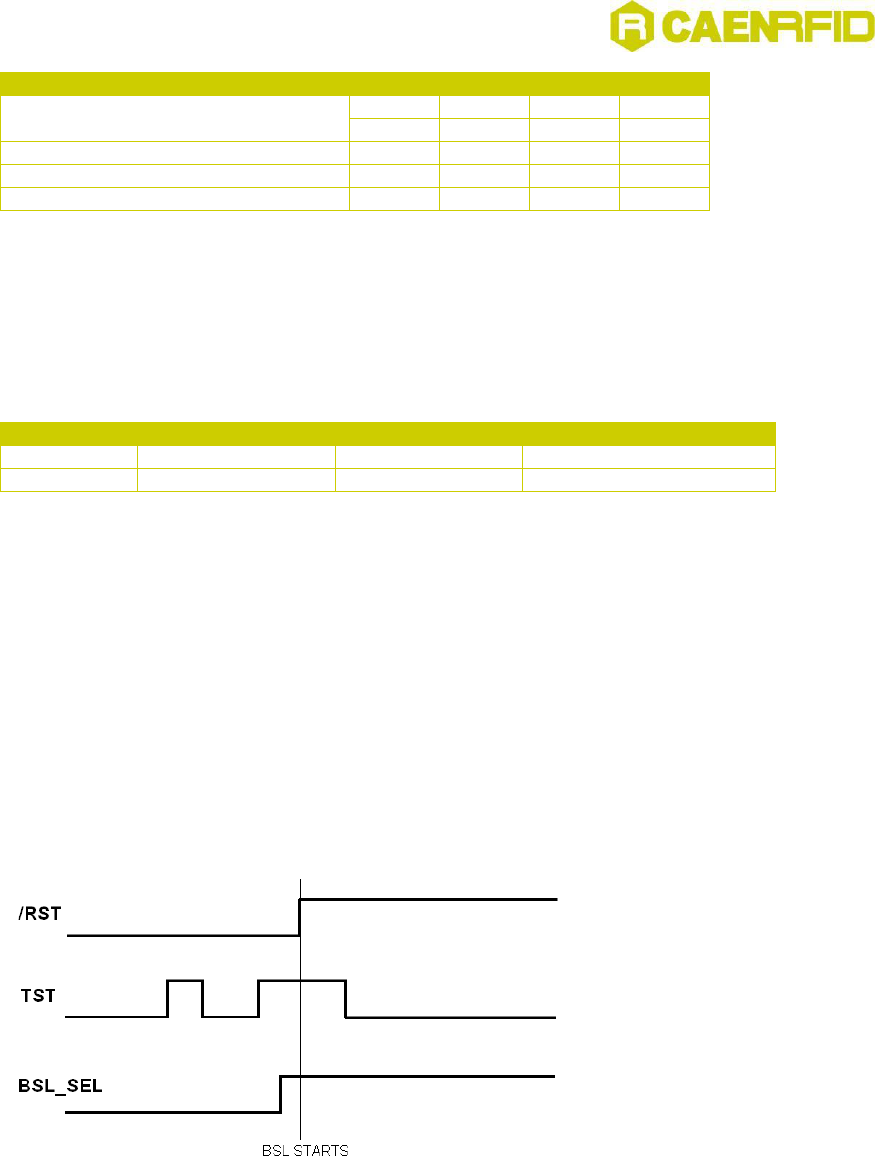
In order to start the BSL of Quark internal microcontroller /RST, TST and BSL_SEL signal shall be driven as in the picture
below:
Fig. 2.7: BSL sequence
The BSL program execution starts when TST pin has received a minimum of two positive transitions and if TST is high
while /RST rises from low to high. BSL_SEL shall be at high level before BSL starts. Pulses length and distance between
edges of all signals shall be 10ms at least.
QUARK R1230CB - R1230BEVB - R1230ADAT - Technical Information Manual
17
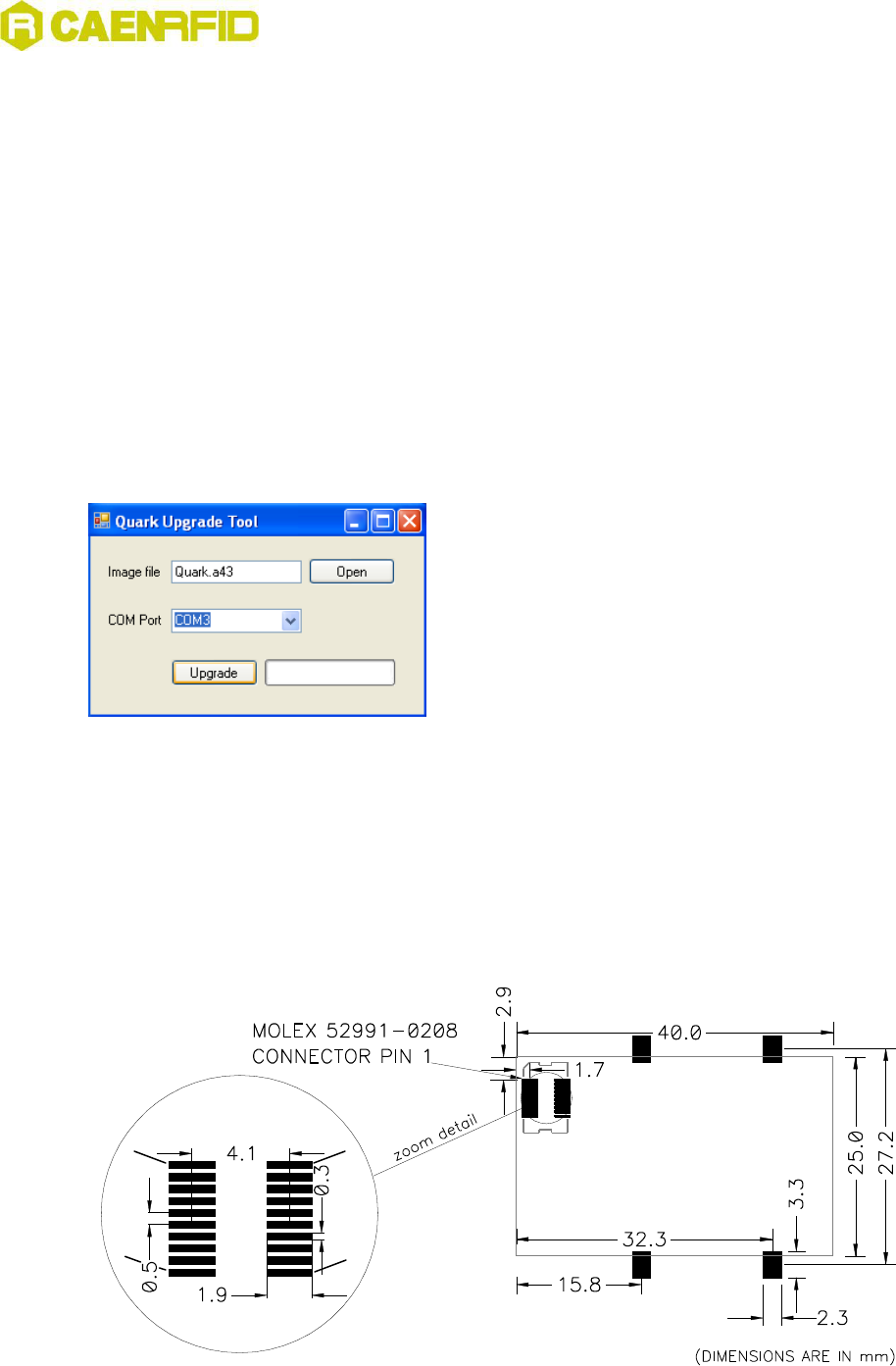
Firmware upgrade via R1230CBEVB board
Quark firmware upgrade can be managed via USB by using the evaluation board (mod.R1230CBEVB) and the SW
upgrade program.
In order to upgrade the firmware follow the steps below:
- Connect to the USB port the evaluation board with the Quark reader installed
- Verify the virtual COM port associated to the board
- Open the FW upgrade program
- Select the COM port
- Select the image file by clicking on “Open” button
- Click on “Upgrade” button
- Disconnect the USB cable from the evaluation board
- Connect again the USB cable in order to restore normal reader operation.
Fig. 2.8: QUARK R1230CB upgrade program window
PCB Pad Layout
In the picture below the recommended PCB pad layout to be implemented on the user host board is shown. The 4
square pads shall be used to solder R1230CB shield and shall be connected to ground. In addition is shown the position
and the layout required for Molex 52991-0208 connector, which mates with R1230CB supply and I/O connector, and
which shall be soldered on the host board.
Fig. 2.9: PCB pad layout
1
19
2
20

QUARK R1230CB - R1230BEVB - R1230ADAT - Technical Information Manual
18
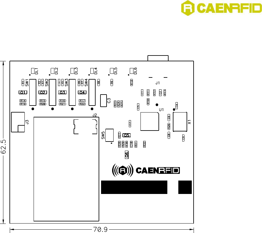
3 Quark R1230CBEVB
This Chapter provide the basic information to work with the Quark R1230CBEVB Evaluation
Board. It contains these topics:
Technical Specifications Table
Connection diagram
Technical drawings
Electrical scheme
External Connections
QUARK R1230CB - R1230BEVB - R1230ADAT - Technical Information Manual
19
Technical Specifications Table
Switch
SW1= RESET
SW2...SW5=GPIO
USB Port
USB Type A plug connector
Bus powered USB 2.0 device
Must be connected to Hight-power Port (500 mA @ VBUS)
It appears as USB serial port
Virtual Com Port (VCP) drivers for Windows XP/Vista/Seven (7), Windows
CE 4.2, Linux 2.40 and greater
Baudrate: 115200
Databits: 8
Stopbits: 1
Parity: none
Flow control: none
User Interface
Red LED: Power
Yellow LED: USB communication activity
Green LED: GPIO[0..3].
Dimensions
(W)70.9 x (L)62.5 x (H)11.6 mm3
(2.8 x 2.5 x 0.5 inch3)
Electrical Power
DC Voltage 5V +/-5%
Max 400 mA5
Operating Temperature
-10 °C to +55 °C
Tab. 3.1: QUARK R1230CBEVB Technical Specifications
Connection diagram
The following block diagram shows how to connect the Mod. R1230CB with the PC host via the Mod. R1230CBEVB evaluation board.
5 With Quark reader operating.
Antenna
USB
R1230CBEVB
Molex Connector
R1230CB
OEM UHF
Multiregional Ultra
Compact Reader
to host

QUARK R1230CB - R1230BEVB - R1230ADAT - Technical Information Manual
22
External Connections
GPIO connector pinout is shown in the following table:
Pin #
Signal
1
GPIO 1
2
GPIO 0
3
GPIO 2
4
GPIO 3
5
GND
6
GND
Tab. 3.2: QUARK R1230CBEVB connector pinout

QUARK R1230CB - R1230BEVB - R1230ADAT - Technical Information Manual
23
4 Quark R1230ADAT
This Chapter provide the basic information to work with the Quark R1230ADAT Adapter
Board. It contains these topics:
Technical Specifications Table
Technical drawings
Electrical scheme
External Connections
QUARK R1230CB - R1230BEVB - R1230ADAT - Technical Information Manual
24
Technical Specifications Table
Digital I/O
Four I/O lines 3.3 V out @ 3mA
UART Serial Port
Baudrate: 115200
Databits: 8
Stopbits: 1
Parity: none
Flow control: none
3.3 V I/O voltage level
9.6÷115 kbit/s data rate (settable)
Dimensions
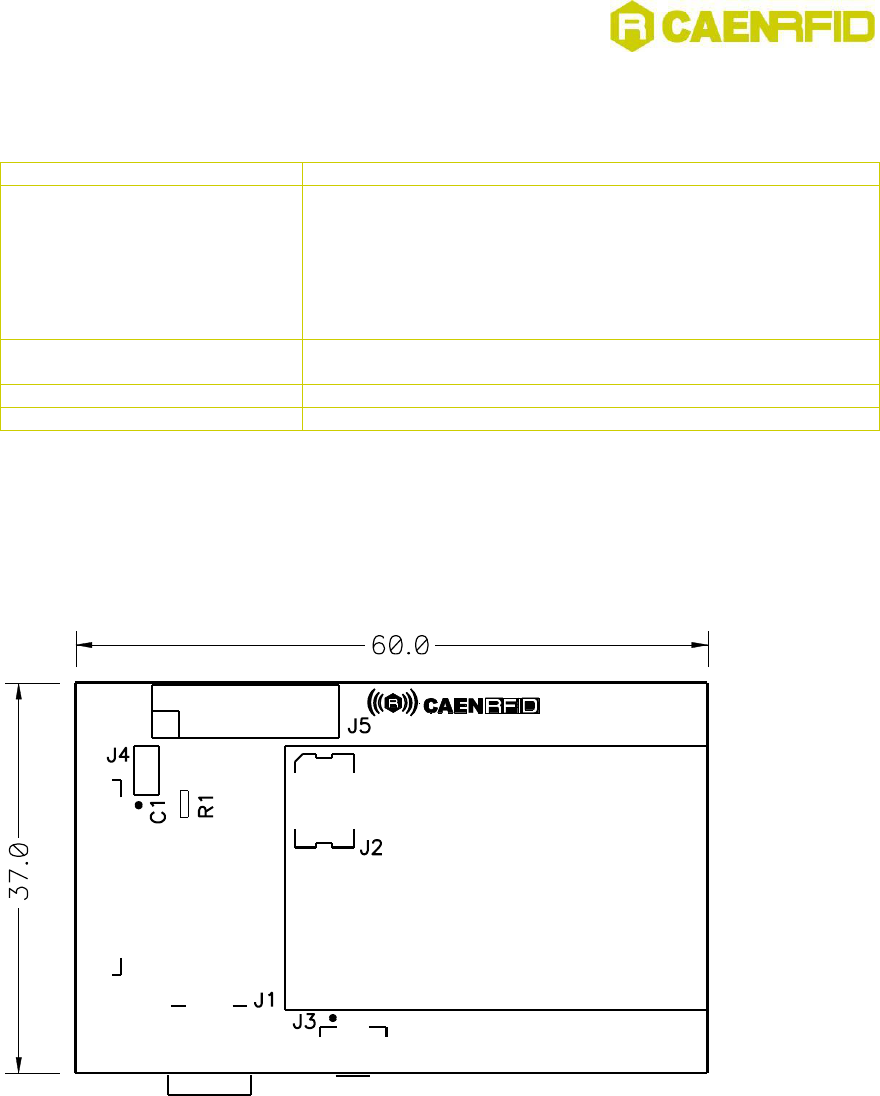
(W)60 x (L)37 x (H)4.6 mm3
(2.4 x 1.5 x 0.2 inch3)
Supply Voltage Range
2.5V ÷ 5.5V
Operating Temperature
-10 °C to +55 °C
Tab. 4.1: QUARK R1230ADAT Technical Specifications
Technical drawings
The location of the connector is shown in Fig. 4.1. The mechanical specifications are listed below:
Fig. 4.1: Quark R1230ADAT technical drawing
QUARK R1230CB
mounting location

QUARK R1230CB - R1230BEVB - R1230ADAT - Technical Information Manual
26
External Connections
Supply and I/O connector pinout is shown in the following table:
Pin #
Signal
Description
1
VIN
Input supply voltage
2
/RST
Reset (active low)
3
GPIO0
General Purpose IO #0
4
GPIO1
General Purpose IO #1
5
GPIO2
General Purpose IO #2
6
GPIO3
General Purpose IO #3
7
NC
Not connected
8
NC
Not connected
9
RXD
UART RX from host
10
TXD
UART TX to host
11
GND
Ground
12
GND
Ground
Tab. 4.2: QUARK R1230ADAT connector pinout

QUARK R1230CB - R1230BEVB - R1230ADAT - Technical Information Manual
27
5 Quark Regulatory Compliance

QUARK R1230CB - R1230BEVB - R1230ADAT - Technical Information Manual
28
FCC Compliance
This equipment has been tested and found to comply with Part 15 of the FCC Rules.
NOTE:
(a) Any changes or modification not approved by CAEN RFID could void the user’s authority to operate the
equipment.
(b) The QUARK R1230CB Module, which is rated at 200 mW output, is approved for operation with the CAENRFID
antenna Mod. WANTENNAX012 (Linear polarized antenna 1.3dBi gain 902 - 928 MHz). Use of other than the approved
antenna with this unit may result in harmful interference with other users, and cause the unit to fail to meet regulatory
requirements.
(c) The QUARK R1230CB transmitter module is approved for battery operation. In case that the module is
embedded inside a device powered by AC line, the overall equipment shall be tested to comply with Section 15.207
requirements.