DETECTION MONITORING TECHNOLOGIES AIMSFS-05X AIMS FAST SCAN RADAR SYSTEM (AIMSFS-05X) User Manual MSM855 Detailed
DETECTION MONITORING TECHNOLOGIES, LLC (dba DMT, LLC) AIMS FAST SCAN RADAR SYSTEM (AIMSFS-05X) MSM855 Detailed
Contents
User Manual 1A
DIGITAL-LOGIC AG MSM855/HLV/B/B2 Detailed Manual V1.0A
2
For internal use only:
File: MSM855_Detailed_V1.0A
Path: R:\HANDBUCH\MSM\cpu_boards\MSM855\MSM855_Detailed_V1.0A.doc
COPYRIGHT
2008 BY DIGITAL-LOGIC AG
This publication is protected by copyright and all rights are reserved. No part of this document may be
reproduced, transmitted, transcribed or stored in a retrieval system, in any form or by any means, electronic,
mechanical, optical, manual, or otherwise, without the prior written permission of DIGITAL-LOGIC AG.
The software described herein, together with this document, are furnished under a license agreement and
may be used or copied only in accordance with the terms of that agreement.
About this Manual and How to Use It
This manual is written for the original equipment manufacturer (OEM) who plans to build computer systems
based on the single board MICROSPACE-PC. It is for integrators and programmers of systems based on the
MICROSPACE-Computer family. This manual provides instructions for installing and configuring the board,
and describes the system and setup requirements. This document contains information on hardware
requirements, interconnections, and details of how to program the system. Please check the Product CD for
further information and manuals.
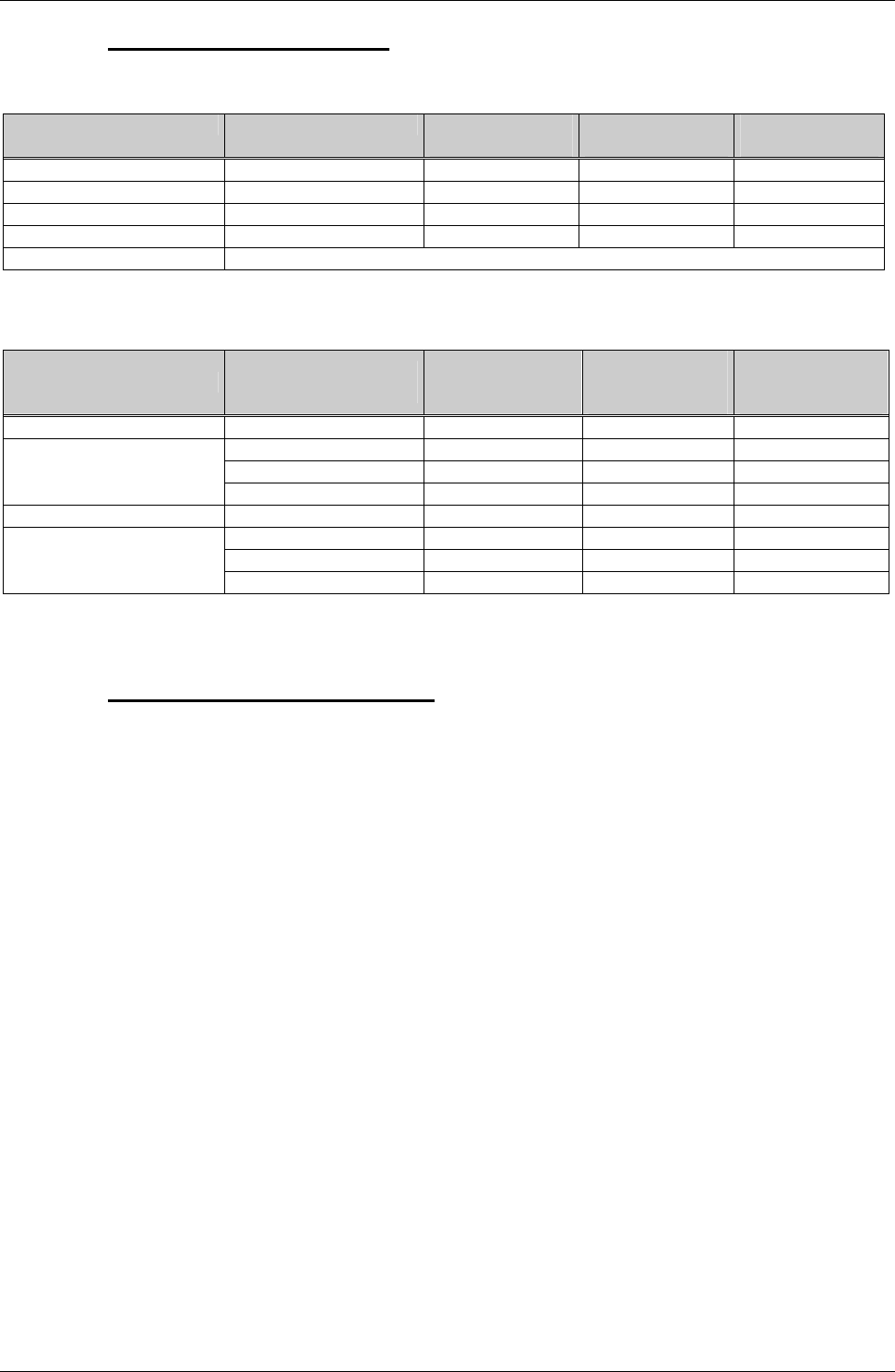
REVISION HISTORY:
Document
Version
Date/Initials: Modification:
Remarks, News, Attention:
V1.0 02.2008 WAS Initial Version of Detailed Manual adapted from existing V1.4C
Sections 1.12, 1.13 added / 2.11.1 & 2.11.2 updated
V1.0A 07.2008 DAR Chapter 5.3.6 / 9.71
Attention!
1. All information in this manual, and the product, are subject to change without prior notice.
2. Read this manual prior to installation of the product.
3. Read the security information carefully prior to installation of the product.

DIGITAL-LOGIC AG MSM855/HLV/B/B2 Detailed Manual V1.0A
3
Table of Contents
1. PREFACE .....................................................................................................................................................6
1.1. Trademarks ..................................................................................................................................... 6
1.2. Disclaimer ....................................................................................................................................... 6
1.3. Environmental Protection Statement ........................................................................................... 6
1.4. Who should use this Product ....................................................................................................... 6
1.5. Recycling Information.................................................................................................................... 7
1.6. Technical Support .......................................................................................................................... 7
1.7. Limited Two Year Warranty........................................................................................................... 7
1.8. Explanation of Symbols................................................................................................................. 8
1.9. Applicable Documents and Standards ........................................................................................ 9
1.10. For Your Safety............................................................................................................................. 10
1.11. RoHS Commitment....................................................................................................................... 10
1.11.1. RoHS Compatible Product Design ........................................................................................ 11
1.11.2. RoHS Compliant Production Process ................................................................................... 11
1.11.3. WEEE Application.................................................................................................................. 11
1.12. Swiss Quality ................................................................................................................................ 12
1.13. The Swiss Association for Quality and Management Systems............................................... 12
2. OVERVIEW .................................................................................................................................................13
2.1. Standard Features........................................................................................................................ 13
2.2. Unique Features ........................................................................................................................... 13
2.3. Standards ...................................................................................................................................... 13
2.4. Block Diagrams ............................................................................................................................ 14
2.4.1. SM855 ................................................................................................................................... 14
2.4.2. MSM855 ................................................................................................................................ 14
2.4.3. MSM855B.............................................................................................................................. 15
2.4.4. MSM855B2 ............................................................................................................................ 15
2.5. Specifications ............................................................................................................................... 16
2.6. Dimensions and Diagrams .......................................................................................................... 19
2.6.1. MSM855/B/B2 (all versions) .................................................................................................. 19
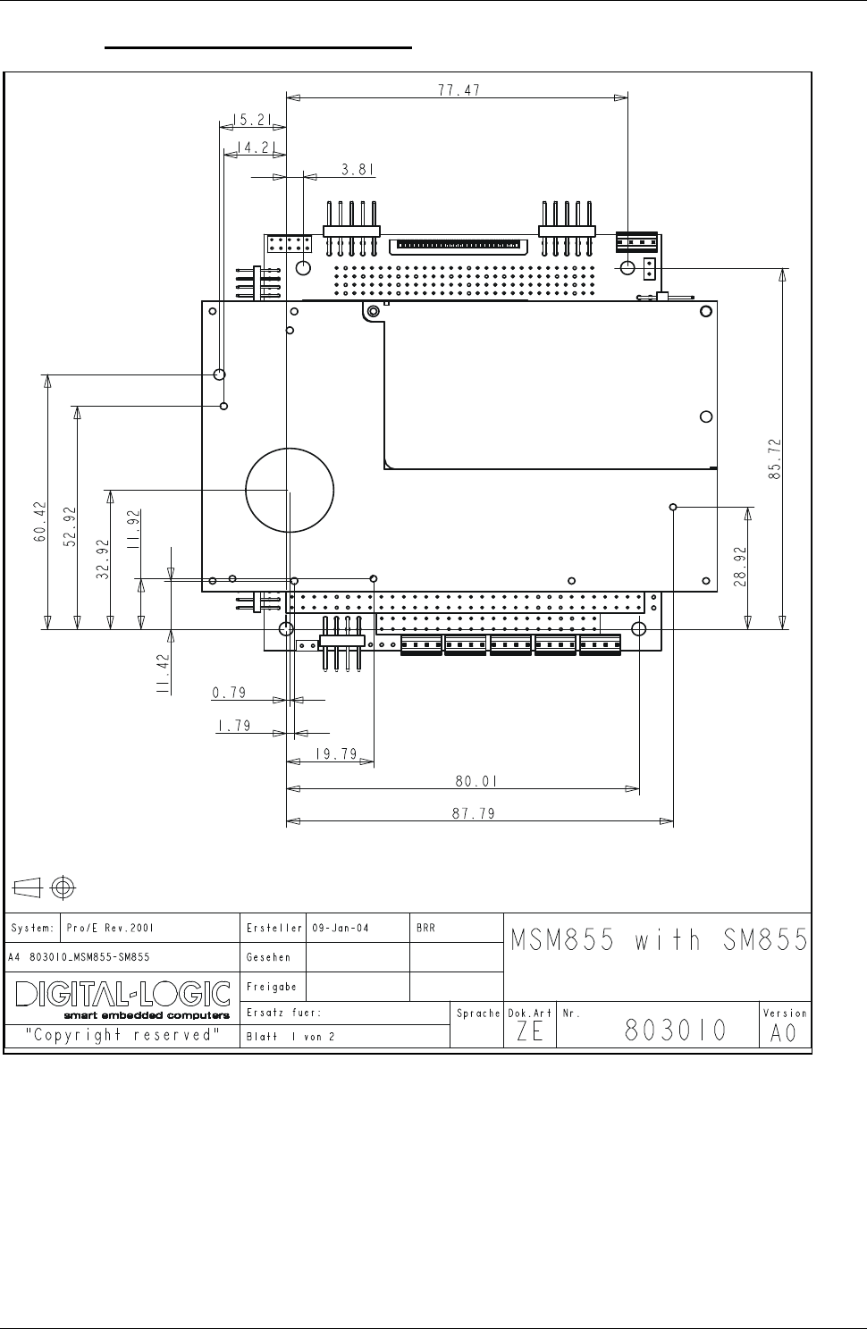
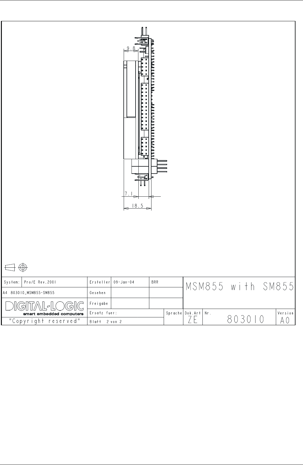
2.6.2. MSM855/B/B2 with SM855.................................................................................................... 20
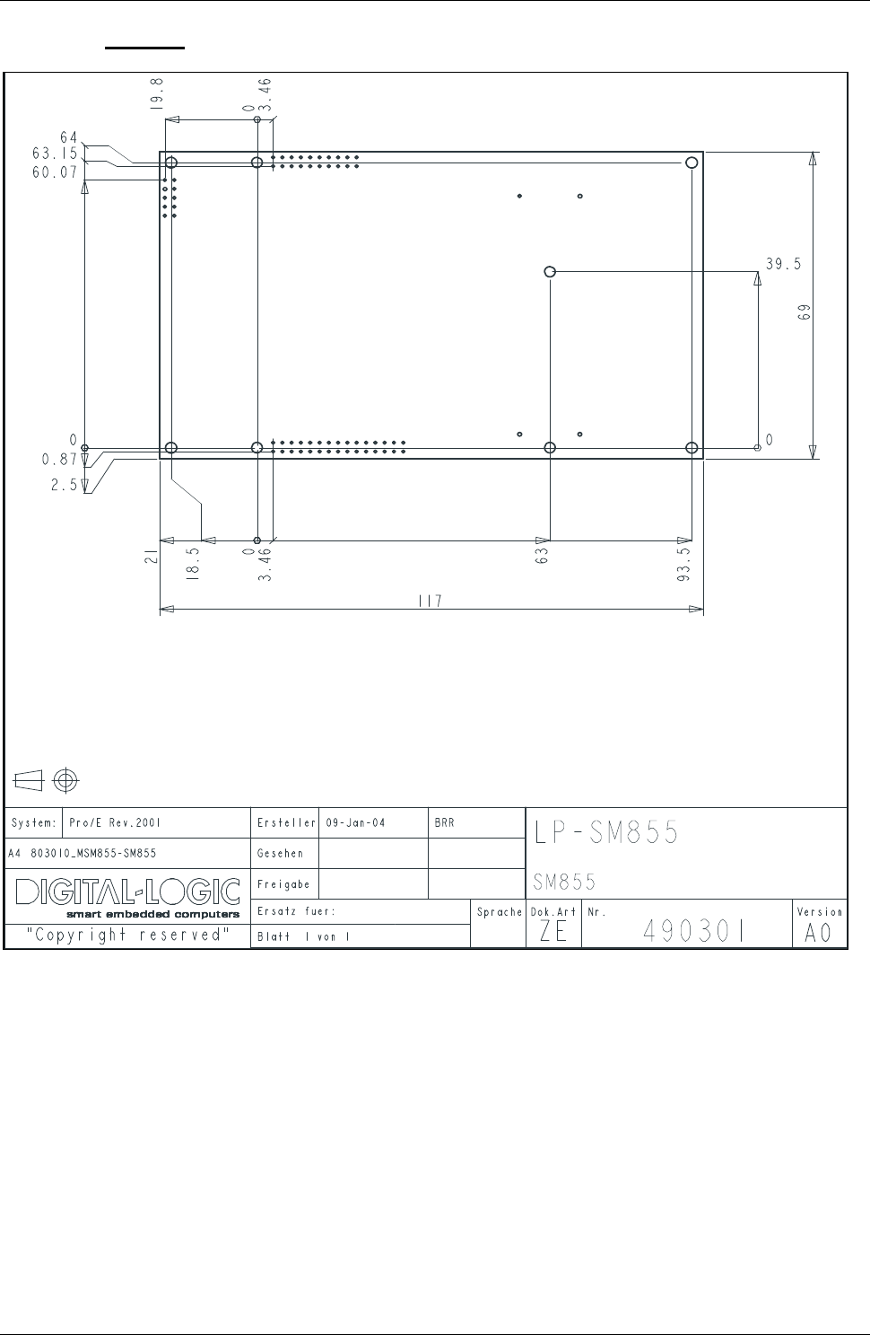
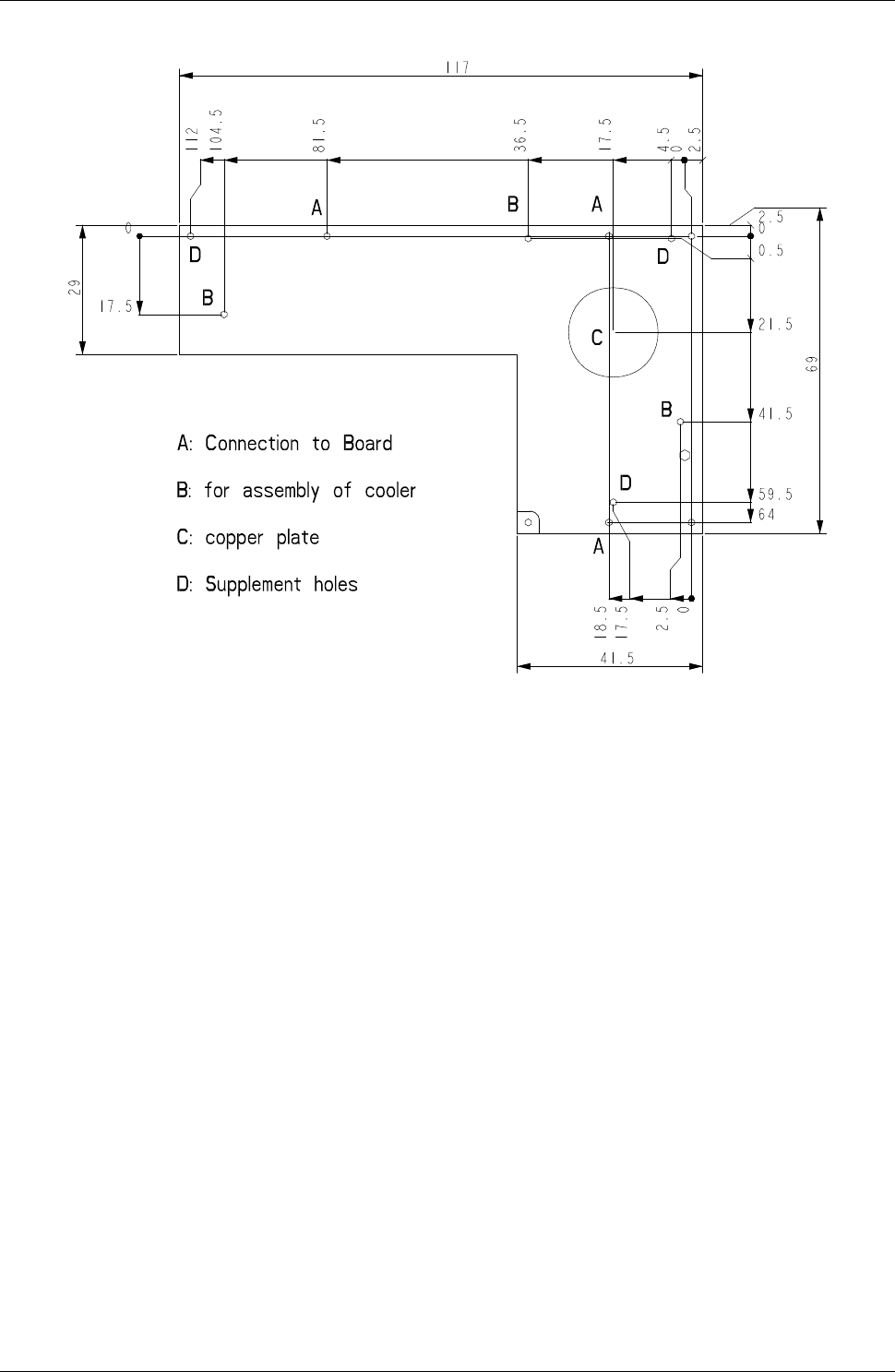
2.6.3. SM855 ................................................................................................................................... 22
2.6.4. MSM855 LANCON ................................................................................................................ 24
2.6.5. MSM855 USB connector PCB............................................................................................... 26
2.6.6. MSM855 AUDIO/SPDIF connector PCB............................................................................... 27
2.6.7. MSM855-CKCON (USB-, AUDIO- and LAN connector print) ............................................... 28
2.6.8. MSM855-DVICON V1.0......................................................................................................... 29
2.7. MSM855/B/B2 Incompatibilities to a standard PC/AT............................................................... 31
2.7.1. MSM855 / HLV ...................................................................................................................... 31
2.7.2. ISA-Incompatibilitiy with ISA-PCCARD-Controller ................................................................ 31
2.7.3. ISA-Incompatibilitiy with 16bit I/O Transfer with FPGA-Decoder .......................................... 32
2.7.4. ISA-Incompatibilitiy with 16bit Memory Transfer with FPGA-Decoder .................................. 32
2.7.5. Compatibilitiy with DIGITAL-LOGIC Peripheral ISA-Boards ................................................. 32
2.8. MSM855/B/B2/HLV Related Application Notes.......................................................................... 32
2.9. Thermoscan .................................................................................................................................. 33
2.10. High Frequency Radiation (to meet EN55022/EN61000) .......................................................... 35
2.10.1. For Peripheral Cables:........................................................................................................... 35
2.10.2. For Stack-Through Applications: ........................................................................................... 35
2.10.3. Power Supply:........................................................................................................................ 35
2.11. RTC Battery Lifetime.................................................................................................................... 36
2.11.1. Maxell ER3 (MSM855) .......................................................................................................... 36
2.11.2. BR1225 (MSM855B/B2) ........................................................................................................ 37
2.11.3. External Battery Assembly .................................................................................................... 37
3. CHIPSET DESCRIPTION ...............................................................................................................................38
3.1. INTEL Processor Pentium-M....................................................................................................... 38
3.1.1. Introduction ............................................................................................................................ 39
3.1.2. Deep Sleep State................................................................................................................... 39
3.1.3. Low Power Features.............................................................................................................. 39
3.1.4. Deeper Sleep State ............................................................................................................... 39
3.1.5. Enhanced Intel® SpeedStep® Technology............................................................................. 40

DIGITAL-LOGIC AG MSM855/HLV/B/B2 Detailed Manual V1.0A
4
3.2. Graphic-Memory-Control Hub: INTEL 855GME........................................................................ 41
3.2.1. Processor Host Interface ....................................................................................................... 41
3.2.2. Intel 855GME GMCH Host Bus Error Checking.................................................................... 41
3.2.3. Intel 855GME GMCH System Memory Interface .................................................................. 41
3.2.4. Intel 855GME GMCH Internal Graphics ................................................................................ 42
3.2.5. Intel 855GME GMCH Analog Display Port............................................................................ 42
3.2.6. Intel 855GME GMCH Integrated DVO Ports ......................................................................... 42
3.2.7. Hub Interface ......................................................................................................................... 42
3.2.8. Address Decode Policies....................................................................................................... 42
3.3. IO Control Hub Intel-ICH4M / ICH4.............................................................................................. 43
4. BUS SIGNALS ............................................................................................................................................45
4.1. PC104 Bus..................................................................................................................................... 45
4.2. Expansion Bus ............................................................................................................................. 47
4.3. Addressing PCI Devices.............................................................................................................. 48
4.3.1. MSM855/HLV ........................................................................................................................ 48
4.3.2. MSM855B/B2:........................................................................................................................ 49
5. DETAILED SYSTEM DESCRIPTION ................................................................................................................50
5.1. Power Requirements.................................................................................................................... 50
5.1.1. Power Supply Cords.............................................................................................................. 50
5.1.2. Typical Power Consumption.................................................................................................. 51
5.1.3. Minimum Power-Off Time...................................................................................................... 51
5.1.4. ATX–Compatible Power Function ......................................................................................... 51
5.1.5. MSM855-HLV-Input (High Level Voltage Input).................................................................... 52
5.1.6. MSMPS104 (PC104 power supply)....................................................................................... 53
5.2. Boot Time...................................................................................................................................... 54
5.3. Interfaces ...................................................................................................................................... 54
5.3.1. AT Compatible Keyboard and PS/2 Mouse........................................................................... 54
5.3.2. Line Printer Port LPT1 ........................................................................................................... 54
5.3.3. Serial Ports COM1-COM2 ..................................................................................................... 55
5.3.4. Floppy Disk Interface............................................................................................................. 55
5.3.5. Speaker Interface .................................................................................................................. 56
5.3.6. 6 Port USB V2.0 .................................................................................................................... 57
5.3.7. Console Redirection .............................................................................................................. 58
5.4. Controllers .................................................................................................................................... 59
5.4.1. Interrupt Controllers............................................................................................................... 59
5.5. Timers and Counters ................................................................................................................... 59
5.5.1. Programmable Timers ........................................................................................................... 59
5.5.2. Watchdog............................................................................................................................... 59
5.6. BIOS............................................................................................................................................... 60
5.6.1. BIOS History.......................................................................................................................... 60
5.6.2. Core BIOS Download ............................................................................................................ 61
5.6.3. ROM-BIOS Sockets............................................................................................................... 62
5.7. CMOS RAM Map ........................................................................................................................... 62
5.8. EEPROM Saved CMOS Setup ..................................................................................................... 67
5.8.1. EEPROM Memory for Setup ................................................................................................. 67
5.9. Memory & I/O Map ........................................................................................................................ 68
5.9.1. Replacement of the SODIMM-DDRAM ................................................................................. 68
5.9.2. System I/O Map..................................................................................................................... 70
5.10. VGA / LCD ..................................................................................................................................... 71
5.11. LVDS-Display................................................................................................................................ 73
5.12. LAN / Ethernet .............................................................................................................................. 73
5.12.1. LAN Cable Connection .......................................................................................................... 73
5.12.2. Boot from LAN ....................................................................................................................... 74
5.13. AC97 Sound .................................................................................................................................. 75
5.13.1. Audio Cable Connection........................................................................................................ 75
5.13.2. Sound Settings ...................................................................................................................... 75
5.14. SpeedStep Performance Control................................................................................................ 76
5.14.1. Set up Power Management ................................................................................................... 76
6. DESCRIPTION & LOCATION OF THE CONNECTORS........................................................................................78
6.1. Top Side of the MSM855 V1.2/V1.3 ............................................................................................. 79
6.2. Bottom Side of the MSM855 V1.2/V1.3 ....................................................................................... 80

DIGITAL-LOGIC AG MSM855/HLV/B/B2 Detailed Manual V1.0A
5
6.3. Top Side of the MSM855B/B2 V1.1 ............................................................................................. 81
6.4. Top Side of the MSM855B/B2 V1.1 ............................................................................................. 81
7. JUMPER LOCATIONS ON THE BOARD...........................................................................................................91
7.1. The Jumpers on the MSM855...................................................................................................... 92
7.2. The Jumpers on the MSM855/B2 ................................................................................................ 93
8. LED CRITERIA ...........................................................................................................................................94
9. CABLE INTERFACES ...................................................................................................................................95
9.1. The Hard Disk Cable 44pin.......................................................................................................... 95
9.2. The COM 1/2 Serial Cable ............................................................................................................ 96
9.3. VGA Cable..................................................................................................................................... 96
9.4. The Printer Cable (P4).................................................................................................................. 97
9.5. USB Cable ..................................................................................................................................... 97
9.6. The Micro Floppy Cable............................................................................................................... 98
9.7. The LAN Interface Cable (RJ45).................................................................................................. 99
9.7.1. MSM855 LANCON .............................................................................................................. 100
9.7.2. MSM855B/B2 LANCON ...................................................................................................... 100
10. THERMAL SPECIFICATIONS...................................................................................................................101
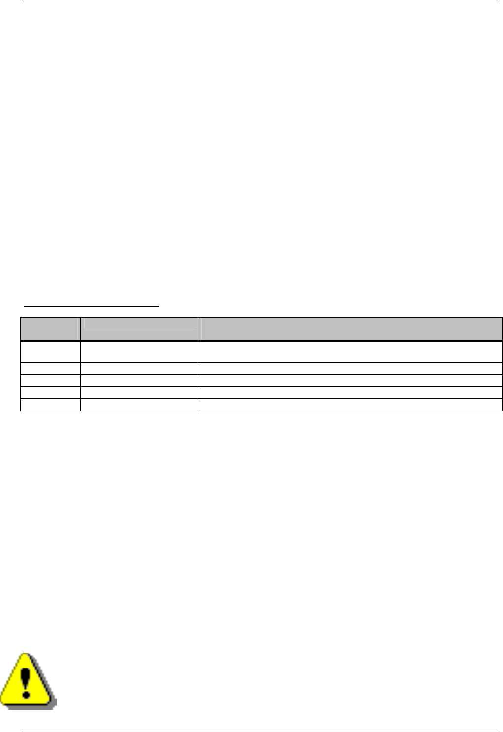
10.1. Thermal Analysis for Case Integration .................................................................................... 101
10.2. Assembly of the Passive Heat Sink.......................................................................................... 102
10.3. Assembly of the Active Heat Sink ............................................................................................ 103
11. ASSEMBLY VIEWS................................................................................................................................104
11.1. MSM855 V1.2 / V1.3 .................................................................................................................... 104
11.2. MSM855B/B2............................................................................................................................... 106
12. Q&A – QUESTIONS & ANSWERS ..........................................................................................................108
13. PREVIOUS PRODUCT VERSIONS............................................................................................................109
13.1. Mechanical Drawing V0.3/V0.4.................................................................................................. 109
13.2. Assembly Views ......................................................................................................................... 110
13.2.1. MSM855 V0.3 / V0.4 ........................................................................................................... 110
13.2.2. MSM855 V1.0 / V1.1 ........................................................................................................... 112
13.3. Connectors & Jumpers.............................................................................................................. 114
13.3.1. MSM855 V0.3 / V0.4 ........................................................................................................... 114
13.3.2. MSM855 V0.3 / V0.4 – Jumpers only.................................................................................. 116
13.3.3. MSM855 V1.0 / V1.1 ........................................................................................................... 118
13.4. Description of the Connectors for V0.4 ................................................................................... 120
13.5. Description of the Jumpers for V0.4 ........................................................................................ 121
14. INDEX ..................................................................................................................................................122

DIGITAL-LOGIC AG MSM855/HLV/B/B2 Detailed Manual V1.0A
6
1. PREFACE
The information contained in this manual has been carefully checked and is believed to be accurate; it is
subject to change without notice. Product advances mean that some specifications may have changed.
DIGITAL-LOGIC AG assumes no responsibility for any inaccuracies, or the consequences thereof, that may
appear in this manual. Furthermore, DIGITAL-LOGIC AG does not accept any liability arising from the use or
application of any circuit or product described herein.
1.1. Trademarks
DIGITAL-LOGIC, DIGITAL-LOGIC-Logo, MICROSPACE, and smartModule are registered trademarks
owned worldwide by DIGITAL-LOGIC AG, Luterbach (Switzerland). In addition, this document may include
names, company logos, and registered trademarks which are, therefore, proprietary to their respective
owners.
1.2. Disclaimer
DIGITAL-LOGIC AG makes no representations or warranties with respect to the contents of this manual, and
specifically disclaims any implied warranty of merchantability or fitness, for any particular purpose. DIGITAL-
LOGIC AG shall, under no circumstances, be liable for incidental or consequential damages or related
expenses resulting from the use of this product, even if it has been notified of the possibility of such damage.
1.3. Environmental Protection Statement
This product has been manufactured to satisfy environmental protection requirements wherever possible.
Many of the components used (structural parts, printed circuit boards, connectors, batteries, etc.) are
capable of being recycled. Final disposal of this product after its service life must be accomplished in
accordance with applicable country, state, or local laws or regulations.
1.4. Who should use this Product
Electrical engineers with know-how in PC-technology.
Because of the complexity and the variability of PC-technology, we cannot guarantee that the product
will work in any particular situation or set-up. Our technical support will try to help you find a solution.
Pay attention to electrostatic discharges; use a CMOS protected workplace.
Power supply must be OFF when working on the board or connecting any cables or devices.

DIGITAL-LOGIC AG MSM855/HLV/B/B2 Detailed Manual V1.0A
7
1.5. Recycling Information
All components within this product fulfill the requirements of the RoHS (Restriction of Hazardous Substances
Directive). The product is soldered with a lead free process.
1.6. Technical Support
1. Contact your local DIGITAL-LOGIC Technical Support, in your country.
2. Use the Internet Support Request form at http://support.digitallogic.ch/ embedded products New
Support Request
Support requests are only accepted with detailed information about the product (i.e., BIOS-, Board-
version)!
1.7. Limited Two Year Warranty
DIGITAL-LOGIC AG guarantees the hardware and software products it manufactures and produces to be
free from defects in materials and workmanship for two years following the date of shipment from DIGITAL-
LOGIC AG, Switzerland. This warranty is limited to the original purchaser of the product and is not
transferable.
During the two year warranty period, DIGITAL-LOGIC AG will repair or replace, at its discretion, any
defective product or part at no additional charge, provided that the product is returned, shipping prepaid, to
DIGITAL-LOGIC AG. All replaced parts and products become property of DIGITAL-LOGIC AG.
Before returning any product for repair, direct customers of DIGITAL-LOGIC AG, Switzerland
are required to register a RMA (Return Material Authorization) number in the Support Center at
http://support.digitallogic.ch/
All other customers must contact their local distributors for returning defective materials.
This limited warranty does not extend to any product which has been damaged as a result of accident,
misuse, abuse (such as use of incorrect input voltages, wrong cabling, wrong polarity, improper or
insufficient ventilation, failure to follow the operating instructions that are provided by DIGITAL-LOGIC AG or
other contingencies beyond the control of DIGITAL-LOGIC AG), wrong connection, wrong information or as
a result of service or modification by anyone other than DIGITAL-LOGIC AG. Nor if the user has insufficient
knowledge of these technologies or has not consulted the product manuals or the technical support of
DIGITAL-LOGIC AG and therefore the product has been damaged.
Empty batteries (external and onboard), as well as all other battery failures, are not covered by this
manufacturer’s limited warranty.
Except, as directly set forth above, no other warranties are expressed or implied, including, but not limited to,
any implied warranty of merchantability and fitness for a particular purpose, and DIGITAL-LOGIC AG
expressly disclaims all warranties not stated herein. Under no circumstances will DIGITAL-LOGIC AG be
liable to the purchaser or any user for any damage, including any incidental or consequential damage,
expenses, lost profits, lost savings, or other damages arising out of the use or inability to use the product.
DIGITAL-LOGIC AG MSM855/HLV/B/B2 Detailed Manual V1.0A
8
1.8. Explanation of Symbols
CE Conformity
This symbol indicates that the product described in this manual is in compliance with all
applied CE standards.
Caution, Electric Shock!
This symbol and title warn of hazards due to electrical shocks (> 60V) when touching
products or parts of them. Failure to observe the precautions indicated and/or prescribed by
the law may endanger your life/health and/or result in damage to your equipment.
Caution, Electric Shock!
This symbol and title warn of hazards due to electrical shocks (> 32V) when touching
products or parts of them. Failure to observe the precautions indicated and/or prescribed by
the law may endanger your life/health and/or result in damage to your equipment
Warning, ESD Sensitive Device!
This symbol and title inform that electronic boards and their components are sensitive to
Electro Static Discharge (ESD). In order to ensure product integrity at all times, care must
always be taken while handling and examining this product.
Attention!
This symbol and title emphasize points which, if not fully understood and taken into
consideration by the reader, may endanger your health and/or result in damage to your
equipment.
Note...
This symbol and title emphasize aspects the user should read through carefully for his, or
her, own advantage.
Warning, Heat Sensitive Device!
This symbol indicates a heat sensitive component.
Safety Instructions
This symbol shows safety instructions for the operator to follow.
This symbol warns of general hazards from mechanical, electrical, and/or
chemical failure. This may endanger your life/health and/or result in damage
to your equipment.

DIGITAL-LOGIC AG MSM855/HLV/B/B2 Detailed Manual V1.0A
9
1.9. Applicable Documents and Standards
The following publications are used in conjunction with this manual. When any of the referenced
specifications are superseded by an approved revision, that revision shall apply. All documents may be
obtained from their respective organizations.
Advanced Configuration and Power Interface Specification Revision 2.0c, August 25, 2003 Copyright
© 1996-2003 Compaq Computer Corporation, Intel Corporation, Microsoft Corporation, Phoenix
Technologies Ltd., Toshiba Corporation. All rights reserved. http://www.acpi.info/
ANSI/TIA/EIA-644-A-2001: Electrical Characteristics of Low Voltage Differential Signaling (LVDS)
Interface Circuits, January 1, 2001. http://www.ansi.org/
ANSI INCITS 361-2002: AT Attachment with Packet Interface - 6 (ATA/ATAPI-6), November 1, 2002.
http://www.ansi.org/
ANSI INCITS 376-2003: American National Standard for Information Technology – Serial Attached
SCSI (SAS), October 30, 2003. http://www.ansi.org/
Audio Codec ’97 Revision 2.3 Revision 1.0, April 2002 Copyright © 2002 Intel Corporation. All rights
reserved. http://www.intel.com/labs/media/audio/
Display Data Channel Command Interface (DDC/CI) Standard (formerly DDC2Bi) Version 1, August
14, 1998 Copyright © 1998 Video Electronics Standards Association. All rights reserved.
http://www.vesa.org/summary/sumddcci.htm
ExpressCard Standard Release 1.0, December 2003 Copyright © 2003 PCMCIA. All rights reserved.
http://www.expresscard.org/
IEEE 802.3-2002, IEEE Standard for Information technology, Telecommunications and information
exchange between systems–Local and metropolitan area networks–Specific requirements – Part 3:
Carrier Sense Multiple Access with Collision Detection (CSMA/CD) Access Method and Physical
Layer Specifications. http://www.ieee.org
IEEE 802.3ae (Amendment to IEEE 802.3-2002), Part 3: Carrier Sense Multiple Access with Collision
Detection (CSMA/CD) Access Method and Physical Layer Specifications, Amendment: Media Access
Control (MAC) Parameters, Physical Layers, and Management Parameters for 10 GB/s Operation.
http://www.ieee.org
Intel Low Pin Count (LPC) Interface Specification Revision 1.1, August 2002 Copyright © 2002 Intel
Corporation. All rights reserved. http://developer.intel.com/design/chipsets/industry/lpc.htm
PCI Express Base Specification Revision 1.1, March 28, 2005, Copyright © 2002-2005 PCI Special
Interest Group. All rights reserved. http://www.pcisig.com/
PCI Express Card Electromechanical Specification Revision 1.1, March 28, 2005, Copyright © 2002-
2005 PCI Special Interest Group. All rights reserved. http://www.pcisig.com/
PCI Local Bus Specification Revision 2.3, March 29, 2002 Copyright © 1992, 1993, 1995, 1998, 2002
PCI Special Interest Group. All rights reserved. http://www.pcisig.com/
PCI-104 Specification, Version V1.0, November 2003. All rights reserved. http://www.pc104.org
PICMG® Policies and Procedures for Specification Development, Revision 2.0, September 14, 2004,
PCI Industrial Computer Manufacturers Group (PICMG®), 401 Edgewater Place, Suite 500,
Wakefield, MA 01880, USA, Tel: 781.224.1100, Fax: 781.224.1239. http://www.picmg.org/
Serial ATA: High Speed Serialized AT Attachment Revision 1.0a January 7, 2003 Copyright © 2000-
2003, APT Technologies, Inc, Dell Computer Corporation, Intel Corporation, Maxtor Corporation,
Seagate Technology LLC. All rights reserved. http://www.sata-io.org/
DIGITAL-LOGIC AG MSM855/HLV/B/B2 Detailed Manual V1.0A
10
Smart Battery Data Specification Revision 1.1, December 11, 1998. www.sbs-forum.org
System Management Bus (SMBus) Specification Version 2.0, August 3, 2000 Copyright © 1994, 1995,
1998, 2000 Duracell, Inc., Energizer Power Systems, Inc., Fujitsu, Ltd., Intel Corporation, Linear
Technology Inc., Maxim Integrated Products, Mitsubishi Electric Semiconductor Company, Power-
Smart, Inc., Toshiba Battery Co. Ltd., Unitrode Corporation, USAR Systems, Inc. All rights reserved.
http://www.smbus.org/
Universal Serial Bus Specification Revision 2.0, April 27, 2000 Copyright © 2000 Compaq Computer
Corporation, Hewlett-Packard Company, Intel Corporation, Lucent Technologies Inc., Microsoft
Corporation, NEC Corporation, Koninklijke Philips Electronics N.V. All rights reserved.
http://www.usb.org/
1.10. For Your Safety
Your new DIGITAL-LOGIC product was developed and tested carefully to provide all features
necessary to ensure its compliance with electrical safety requirements. It was also designed for a
long, fault-free life. However, this life expectancy can be drastically reduced by improper treatment
during unpacking and installation. Therefore, in the interest of your own safety and for the correct
operation of your new DIGITAL-LOGIC product, please comply with the following guidelines.
Attention!
All work on this device must only be carried out by sufficiently skilled personnel.
Caution, Electric Shock!
Before installing your new DIGITAL-LOGIC product, always ensure that your mains power is
switched off. This applies also to the installation of piggybacks or peripherals. Serious
electrical shock hazards can exist during all installation, repair and maintenance operations
with this product. Therefore, always unplug the power cable and any other cables which
provide external voltage before performing work.
Warning, ESD Sensitive Device!
Electronic boards and their components are sensitive to static electricity. In order to ensure
product integrity at all times, be careful during all handling and examinations of this product.
1.11. RoHS Commitment
DIGITAL-LOGIC AG is committed to develop and produce environmentally friendly products according to the
Restriction of Hazardous Substances (RoHS) Directive (2002/95/EC) and the Waste Electrical and Electronic
Equipment (WEEE) Directive (2002/96/EC) established by the European Union. The RoHS directive was
adopted in February 2003 by the European Union and came into effect on July 1, 2006. It is not a law but a
directive, which restricts the use of six hazardous materials in the manufacturing of various types of
electronic and electrical equipment. It is closely linked with the Waste Electrical and Electronic Equipment
Directive (WEEE) 2002/96/EC, which has set targets for collection, recycling and recovery of electrical goods
and is part of a legislative initiative to solve the problem of huge amounts of toxic e-waste.
Each European Union member state is adopting its own enforcement and implementation policies using the
directive as a guide. Therefore, there could be as many different versions of the law as there are states in
the EU. Additionally, non-EU countries like China, Japan, or states in the U.S. such as California may have
their own regulations for green products, which are similar, but not identical, to the RoHS directive.

DIGITAL-LOGIC AG MSM855/HLV/B/B2 Detailed Manual V1.0A
11
RoHS is often referred to as the "lead-free" directive but it restricts the use of the following substances:
Lead
Mercury
Cadmium
Chromium VI
PBB and PBDE
The maximum allowable concentration of any of the above mentioned substances is 0.1% (except for
Cadmium, which is limited to 0.01%) by weight of homogeneous material. This means that the limits do not
apply to the weight of the finished product, or even to a component but to any single substance that could
(theoretically) be separated mechanically.
1.11.1. RoHS Compatible Product Design
All DIGITAL-LOGIC standard products comply with RoHS legislation.
Since July 1, 2006, there has been a strict adherence to the use of RoHS compliant electronic and
mechanical components during the design-in phase of all DIGITAL-LOGIC standard products.
1.11.2. RoHS Compliant Production Process
DIGITAL-LOGIC selects external suppliers that are capable of producing RoHS compliant devices. These
capabilities are verified by:
1. A confirmation from the supplier indicating that their production processes and resulting devices are
RoHS compliant.
2. If there is any doubt of the RoHS compliancy, the concentration of the previously mentioned
substances in a produced device will be measured. These measurements are carried out by an
accredited laboratory.
1.11.3. WEEE Application
The WEEE directive is closely related to the RoHS directive and applies to the following devices:
Large and small household appliances
IT equipment
Telecommunications equipment (although infrastructure equipment is exempt in some countries)
Consumer equipment
Lighting equipment – including light bulbs
Electronic and electrical tools
Toys, leisure and sports equipment
Automatic dispensers
It does not apply to fixed industrial plants and tools. The compliance is the responsibility of the company that
brings the product to market, as defined in the directive. Components and sub-assemblies are not subject to
product compliance. In other words, since DIGITAL-LOGIC does not deliver ready-made products to end
users the WEEE directive is not applicable for DIGITAL-LOGIC. Users are nevertheless encouraged to
properly recycle all electronic products that have reached the end of their life cycle.

DIGITAL-LOGIC AG MSM855/HLV/B/B2 Detailed Manual V1.0A
12
1.12. Swiss Quality
100% Made in Switzerland
DIGITAL-LOGIC is a member of "Swiss-Label"
This product was not manufactured by employees earning
piecework wages
This product was manufactured in humane work conditions
All employees who worked on this product are paid
customary Swiss market wages and are insured
ISO 9000:2001 (quality management system)
1.13. The Swiss Association for Quality and Management
Systems
The Swiss Association for Quality and Management Systems (SQS) provides certification and assessment
services for all types of industries and services. SQS certificates are accepted worldwide thanks to
accreditation by the Swiss Accreditation Service (SAS), active membership in the International Certification
Network, IQNet, and co-operation contracts/agreements with accredited partners.
www.sqs.ch
The SQS Certificate ISO 9001:2000 has been issued to DIGITAL-LOGIC AG, the entire company, in the field
of development, manufacturing and sales of embedded computer boards, embedded computer modules and
computer systems. The certification is valid for three years at which time an audit is performed for
recertification.

DIGITAL-LOGIC AG MSM855/HLV/B/B2 Detailed Manual V1.0A
13
2. OVERVIEW
2.1. Standard Features
The MICROSPACE PC/104 is a miniaturized modular device incorporating the major elements of a PC/AT
compatible computer. It includes standard PC/AT compatible elements, such as:
Powerful PENTIUM -M from 600MHz up to 2GHz
BIOS ROM
DDRAM 128-1024MByte SODIMM 200pin
1024/2048kByte second level cache
Timers
DMA
Real-time clock with CMOS-RAM and 10 year battery buffer
LPT1 parallel port
COM1-, COM2- RS2332 serial port 16C550 comp.
Speaker interface
AT-keyboard interface or PS/2-keyboard interface
Floppy disk interface
AT-IDE hard disk interface
VGA video interface
6 channel sound interface AC97-V2.3
100/10-Base-T LAN (second LAN interface on the MSM855B2 with an Intel 82551ER)
PC/104 embedded BUS (8bit on the MSM855; 8/16bit on the MSM855B/B2)
PS/2 mouse interface
Power management functions AMP and ACPI
6 channel USB V1.1 & V2.0
2.2. Unique Features
The MICROSPACE MSM855 includes all standard PC/AT functions plus unique DIGITAL-LOGIC AG
enhancements, such as:
Single 5Volt supply
Watchdog
Power-fail detection
EEPROM for setup and configuration
IrDA
Optional: Compact Card holder type 1
UL approved parts
Console redirection
2.3. Standards
This MICROSPACE product meets all standards for personal computer architecture.
Standard How to contact the organization Remarks
PC/104BUS www.pc104.org
USB www.usb.org
PCI www.pcisig.com
SMB www.smbus.org
WfM www.intel.com/labs/manage/wfm Wired for management baseline
AC97 www.developer.intel.com/ial/scalableplatforms/audio
LPC www.developer.intel.com/design/chipsets/industry/lpc.htm
ATA/ATAPI-6 www.t13.org
ACPI www.acpi.info Power management
DIGITAL-LOGIC AG MSM855/HLV/B/B2 Detailed Manual V1.0A
14
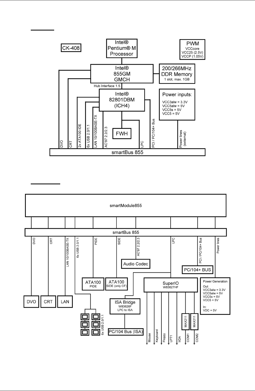
2.4. Block Diagrams
2.4.1. SM855
2.4.2. MSM855
DIGITAL-LOGIC AG MSM855/HLV/B/B2 Detailed Manual V1.0A
15
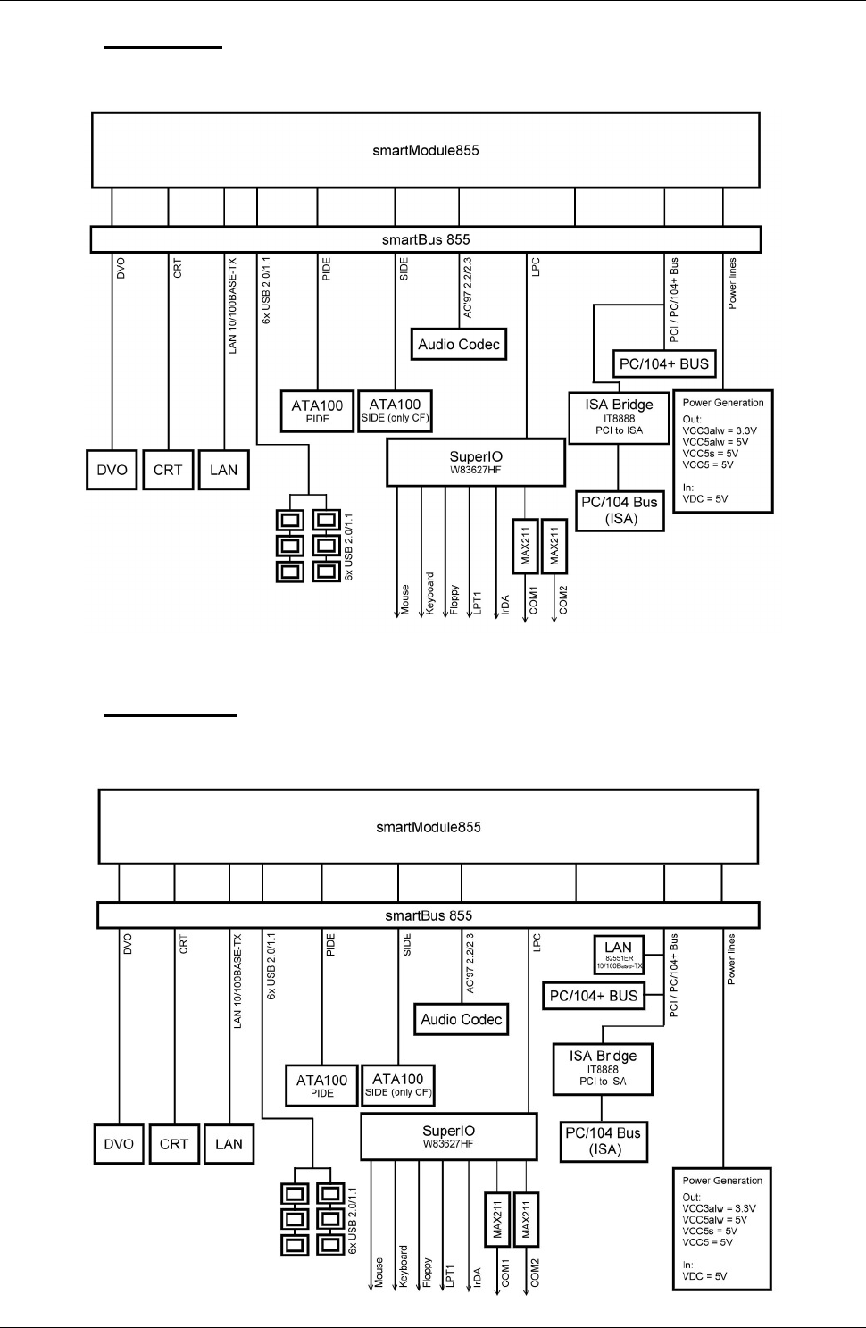
2.4.3. MSM855B
On the MSM855B/B2 there is a PCI to ISA bridge (not an LPC to ISA bridge).
2.4.4. MSM855B2
There is a second LAN chip (Intel 82551ER) assembled on the MSM855B2.

DIGITAL-LOGIC AG MSM855/HLV/B/B2 Detailed Manual V1.0A
16
2.5. Specifications
CPU
CPU Intel® Pentium®-M or Intel® Celeron-M
Compatibility 8086-PentiumM
1st Level Cache 16k data and 16k code
2nd Level Cache 1024/2048kByte
Socket SmartBus855 320pin
Clock MSM855-16 1600MHz (600MHz up to 2GHz available)
FSB 400MHz
Power management Yes, APM2.1 and ACPI 1.2
FPU Integrated
Chipset
Northbridge I from Intel
Southbridge ICH4 from Intel
LAN Integrated (comp. to 82C559 Intel)
On the MSM855B2 is an additional Intel 82551ER.
Audio AC97 – V2.3 5.1-Sound
Firewire IEEE1394 Not on board
Video Intel Extreme Graphics 2
DirectX-9 compatible, 64MByte Video-DDRAM
Memory
Main Memory 1x SODIMM200 socket
SDRAM, 64bit, up to 1024Mbyte stacked
Flash-BIOS 1024kByte Flash
Setup EEPROM 2kByte for CMOS-backup in battery-free applications
Flash-Video BIOS Serial-Flash
Video RAM 16MByte to 64MByte DDRAM
Video
Controller Intel Extreme Graphics 2 is integrated in the Intel 855GME chipset
Memory 64MB
Channel 1 CRT VGA up to 2048 x 1600 pixels
Channel 2 LVDS ,DVI, TV-Out = with the MSM855-DVICON
Bootup-Resolution 640x480 / 800x600 / 1024x768
2D-Graphics Integrated accelerator
3D-Graphics Integrated accelerator
Direct-X, Version 9
PnP Integrated
External Interfaces
Video interfaces CRT1, DVO
USB V1.1/2.0 6 channels
LPT1 IEEE1293 Printer
COM1 RS232
COM2 RS232
Keyboard PS/2
Mouse PS/2
Floppy 26pin FCC Interface for TEAC Mini-floppy
Hard disk 1 channel, 44pin RM2.0mm ATAIDE-cable
Speaker 0.1Watt Speaker
ISA-Bus PC/104
PCI-Bus PC/104plus
LAN 10/100 Base-TX (from the SM855)
LAN 2 10/100 Base-TX (only available on the MSM855B2 with Intel's 82551ER)
DIGITAL-LOGIC AG MSM855/HLV/B/B2 Detailed Manual V1.0A
17
Power Supply MSM855/B/B2
Input voltage Nominal 5V Tolerance +/- 3%
Input inrush current Typically 5Amp, inrush current 15Amp for power-up of 10ms
Protection Not integrated, EMI filter must be added externally
Specification None
3.3Volt power output Not available
Power Supply MSM855-HLV
Input voltage 5-32V (typically 24V) and 5V (tolerance +/- 3%)
Input inrush current
Protection Not integrated, EMI filter must be added externally
Specification MIL-Norm VG 96916-5
3.3Volt power output Not available
Power Consumption
At 5V (with 256MByte)
MSM855-16
typically 2.0Amp (10W) at 600MHz
typically 5.0Amp (25W) at 1600MHz
Standby Typically 0.5Amp
Power-off Typically 40mA
Physical Characteristics PC/104plus
Dimensions Length: 91mm
Depth: 99mm
Height: 25mm
Weight 170gr
Operating Environment
Relative Humidity 5-90% non condensing
IEC68-2-30 at -20° to +50°C, operating
Vibration, operating IEC68-2-6 10-50Hz, 0.075mm and 55-500Hz, 1.0G
Vibration, non-operating IEC68-2-6 10-50Hz, 0.15mm and 55-500Hz, 2.0G
Shock, operating IEC68-2-27 10G, 11ms ½ sine
Shock, non-operating IEC68-2-27 50G, 11ms, ½ sine
Altitude IEC68-2-13 4571meter operating
Temperature, operating IEC68-2-1,2,14 MSM855, standard -20°C to +60°C
Extended Temperature (option)
MIL-810-501/502 see separate table below
Temperature, storage IEC68-2-1,2,14 -65°C to +125°C
The back-up battery is limited on -40°C to
+80°C operating and storage temperatures
Operating Temperature MIL-810-501
MIL-810-502
Extended Temperature Range
MSM855-16 (600MHz)
-40°C to +70°C
Security
e1 Not planned
UL Not planned
ETS 301 Not planned
CE/SEV Yes
Safety AR385-16

DIGITAL-LOGIC AG MSM855/HLV/B/B2 Detailed Manual V1.0A
18
EMI / EMC Tests
Provided all signals are externally filtered and assembled into a closed metallic housing!
EMC Emission EN61000-6-2:2001
Conducted Disturbance EN55022 Class B
Radiated Disturbance EN55022 Class B
EMC Immunity EN61000-6-2
ESD Electrostatic Discharge EN61000-4-2
Voltage = 4kV contact / 8kV air, Criteria A
RF Radiated Field EN61000-4-3
Level = 10V/m, Criteria A
EFT Electrical Fast Transient (Burst) EN61000-4-4
Grade 2: DC-Power lines = 1000V (5/50ns)
Grade 2: AC-Power lines = 2000V (5/50ns)
Grade 2: Signal lines = 500V (5/50ns)
Criteria B
Surge EN61000-4-5
Grade 2: DC-Power lines = 1kV, (1.2/50us)
Grade 2: AC-Power lines = 2kV, (1.2/50us)
Criteria B
Conducted Disturbances EN61000-4-6
Voltage = 10V coupled by case, Criteria A
All information is subject to change without notice.
DIGITAL-LOGIC AG MSM855/HLV/B/B2 Detailed Manual V1.0A
19
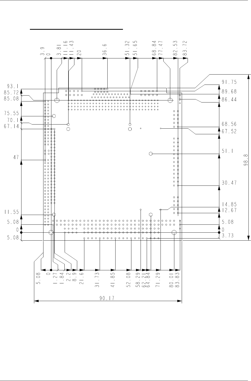
2.6. Dimensions and Diagrams
2.6.1. MSM855/B/B2 (all versions)
DIGITAL-LOGIC AG MSM855/HLV/B/B2 Detailed Manual V1.0A
20
2.6.2. MSM855/B/B2 with SM855
DIGITAL-LOGIC AG MSM855/HLV/B/B2 Detailed Manual V1.0A
21
DIGITAL-LOGIC AG MSM855/HLV/B/B2 Detailed Manual V1.0A
22
2.6.3. SM855
DIGITAL-LOGIC AG MSM855/HLV/B/B2 Detailed Manual V1.0A
23
DIGITAL-LOGIC AG MSM855/HLV/B/B2 Detailed Manual V1.0A
24
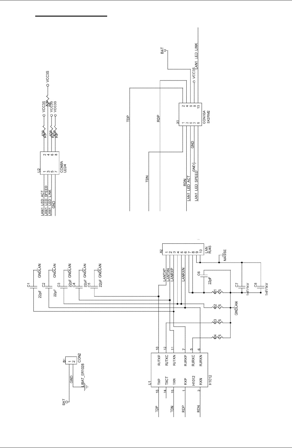
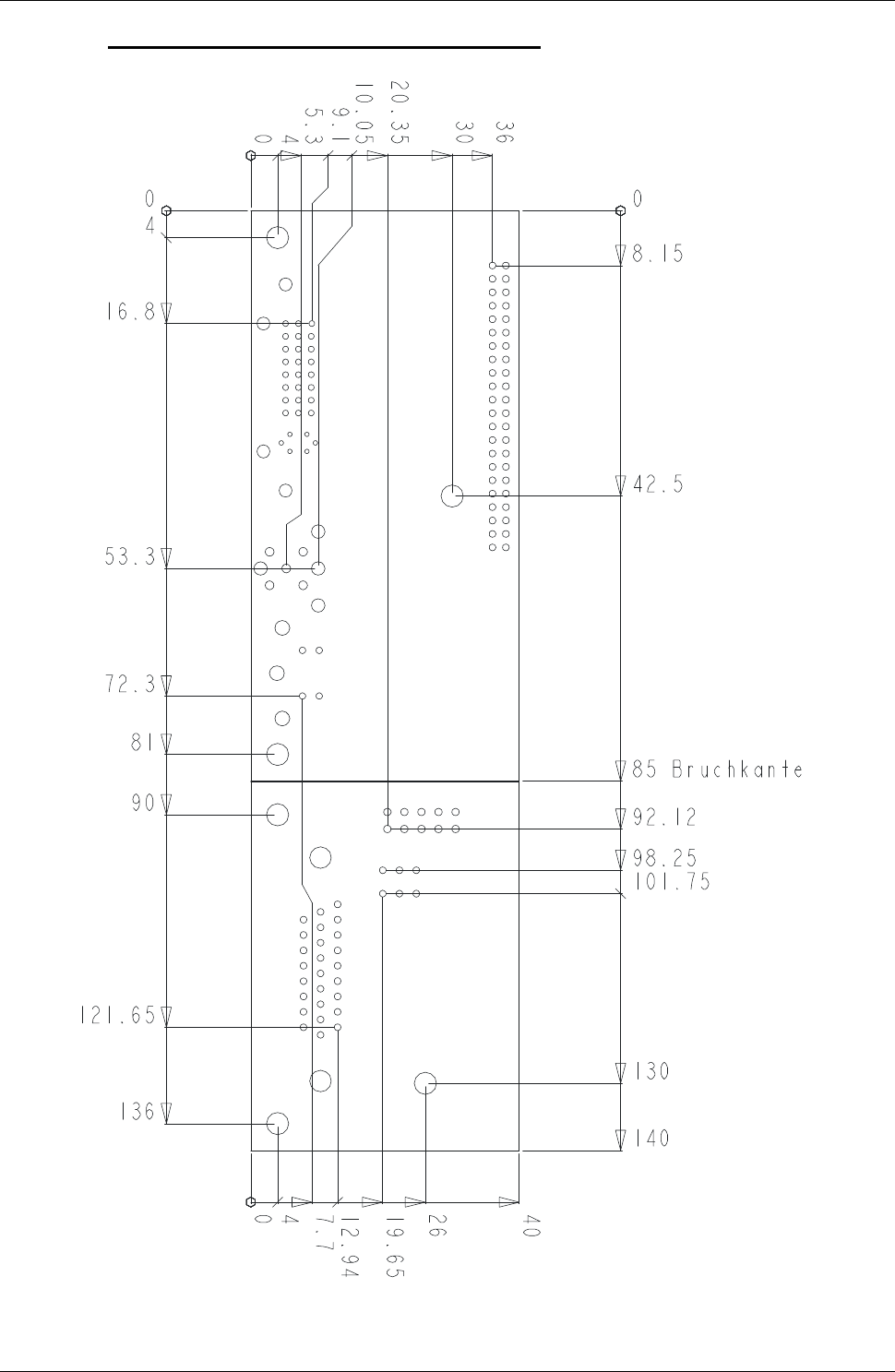
2.6.4. MSM855 LANCON
DIGITAL-LOGIC AG MSM855/HLV/B/B2 Detailed Manual V1.0A
25
2.6.4.1. Mechanical Drawing
DIGITAL-LOGIC AG MSM855/HLV/B/B2 Detailed Manual V1.0A
26
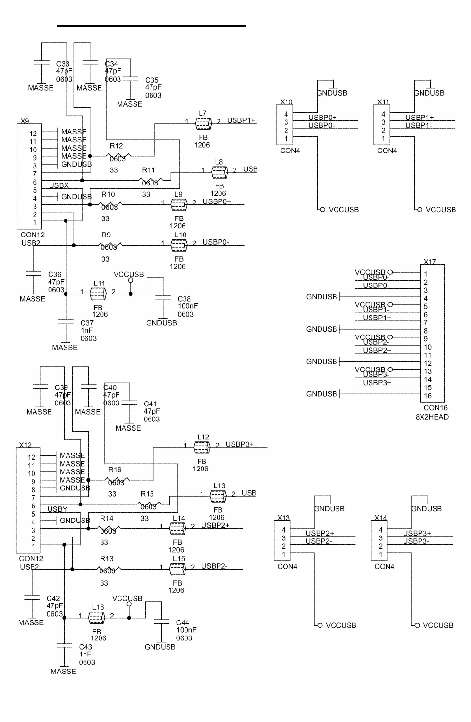
2.6.5. MSM855 USB connector PCB
DIGITAL-LOGIC AG MSM855/HLV/B/B2 Detailed Manual V1.0A
27
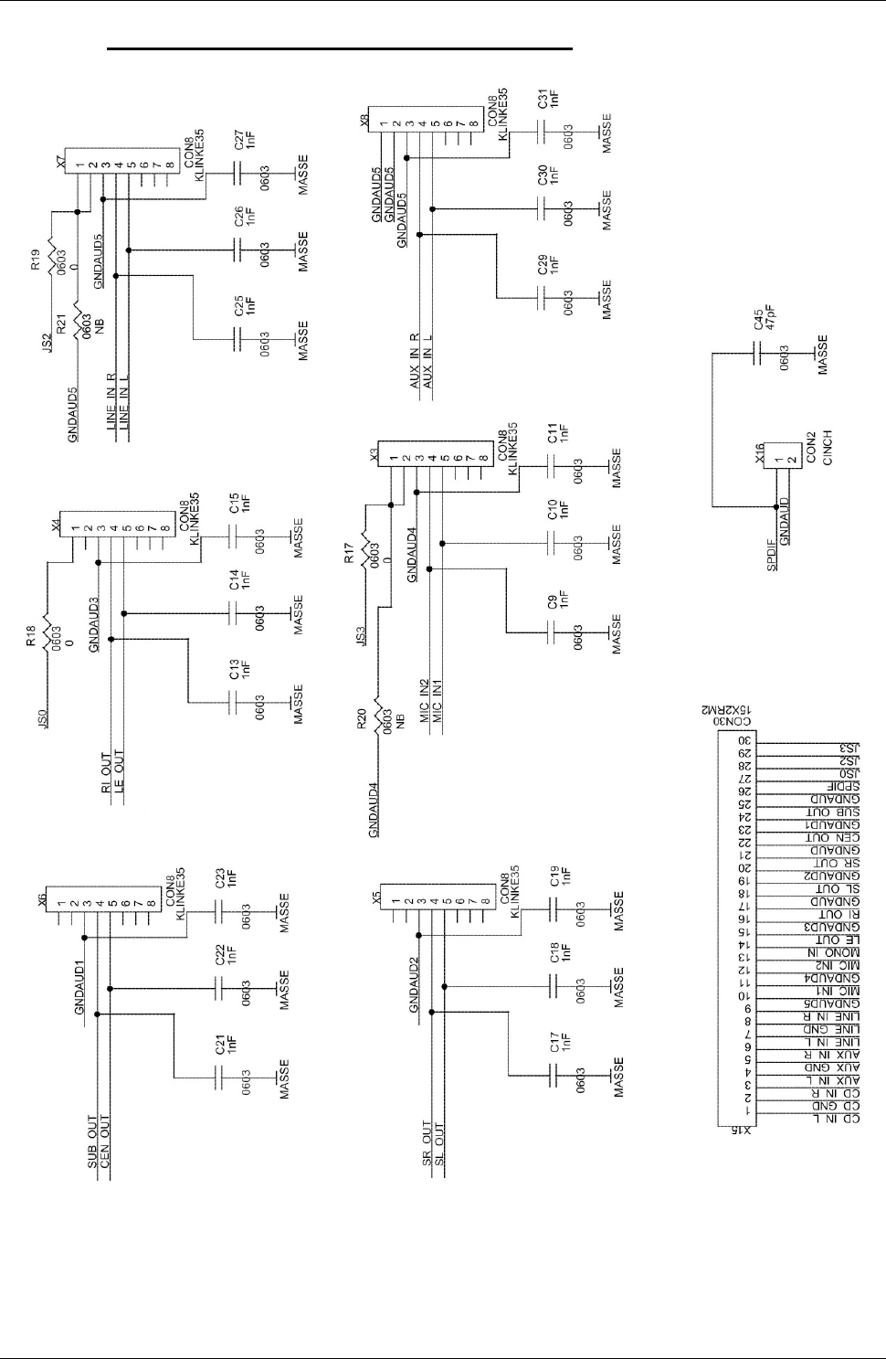
2.6.6. MSM855 AUDIO/SPDIF connector PCB
DIGITAL-LOGIC AG MSM855/HLV/B/B2 Detailed Manual V1.0A
28
2.6.7. MSM855-CKCON (USB-, AUDIO- and LAN connector print)
2.6.7.1. Mechanical Drawing
DIGITAL-LOGIC AG MSM855/HLV/B/B2 Detailed Manual V1.0A
29
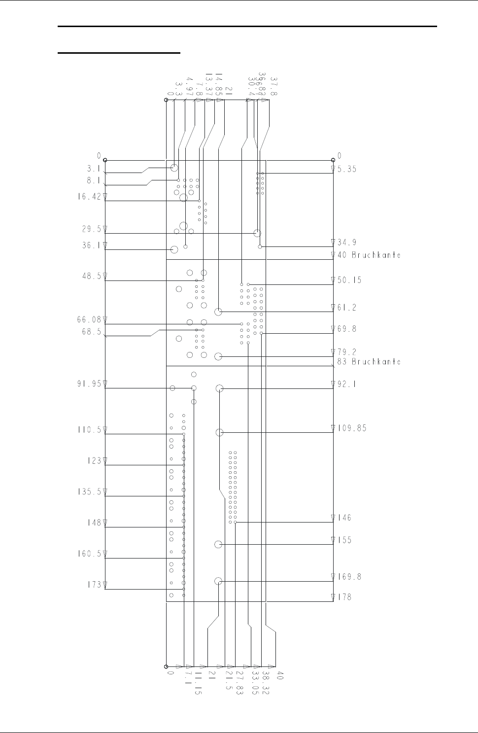
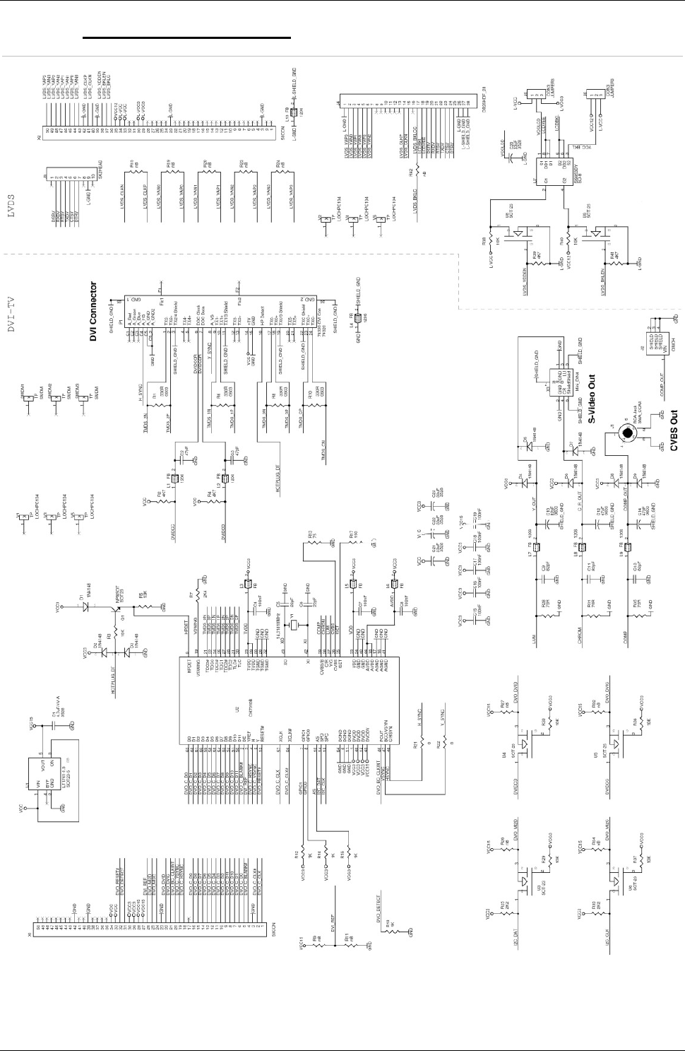
2.6.8. MSM855-DVICON V1.0
DIGITAL-LOGIC AG MSM855/HLV/B/B2 Detailed Manual V1.0A
30
2.6.8.1. MSM855-DVICON mechanical drawing
DIGITAL-LOGIC AG MSM855/HLV/B/B2 Detailed Manual V1.0A
31
2.7. MSM855/B/B2 Incompatibilities to a standard PC/AT
2.7.1. MSM855 / HLV
On the Intel855GME Design and in the PC-03 specification, no ISA-Bus is available. For the BIOS and the
SuperIO functions, the LPC-Bus is integrated. The LPC-Bus is a serialized ISA-Bus with some limitations.
Onboard is an LPC to ISA-Bridge integrated to generate a standard ISA-Bus. In using the combination of the
LPC-Bus and the LPC-Bridge there are some incompatibilities.
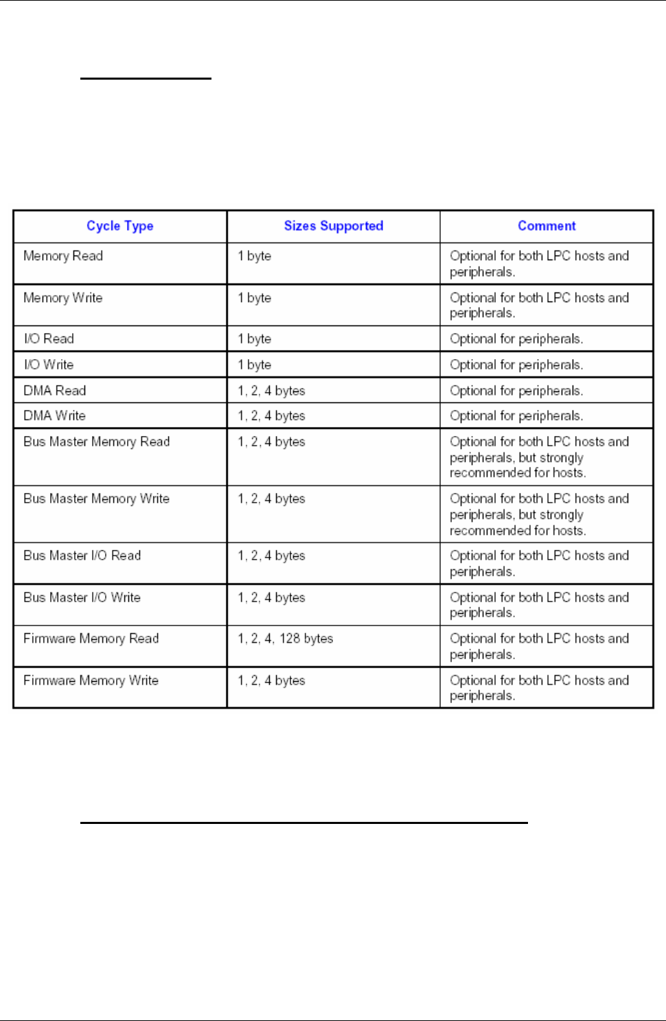
The LPC support the following bus cycles:
This means that all non-Busmaster I/Os and MEM Cycles are only 8bit wide and never 16bit wide. 16bit data
transfer is available in the BusMaster modus only.
2.7.2. ISA-Incompatibilitiy with ISA-PCCARD-Controller
Experience shows that ATA-Drives controlled in an ISA-PCMCIA Controller do not work.
Solution: Use a PCCARD-Controller on the PCI-Bus.
DIGITAL-LOGIC AG MSM855/HLV/B/B2 Detailed Manual V1.0A
32
2.7.3. ISA-Incompatibilitiy with 16bit I/O Transfer with FPGA-Decoder
Our experience shows that 16bit I/O-transfers decoded with an FPGA do not always work correct. Each case
must be tested..
Solution: Use two 8bit transfers instead one 16bit transfer. For time critical transfers we recommend using
the PCI-Bus.
2.7.4. ISA-Incompatibilitiy with 16bit Memory Transfer with FPGA-
Decoder
Experience shows that 16bit Memory-transfers decoded with an FPGA do not always work correctly. Each
case must be tested. Expect problems on odd addresses.
Solution: Use two 8bit transfers instead of one 16bit transfer. For time critical transfers we recommend
using the PCI-Bus.
2.7.5. Compatibilitiy with DIGITAL-LOGIC Peripheral ISA-Boards
Funktion Product Transfer Result Remarks
Serial MSMX104 8bit I/O Works fine -
CAN-Bus MSMCAN104 8bit I/O Works fine -
Ethernet MSME104 16bit I/O Works fine Int. Autoaddressincrement
Video MSMV104 16bit MEM Works fine -
PCMCIA MSMJ104 8/16bit I/O & MEM
Doesn’t work with ATA-Cards
Flash- and SRAM-Cards with
16bit MEM are ok
Sound Card
MSMM104 16bit I/O DMA Works fine
2.8. MSM855/B/B2/HLV Related Application Notes
Application Notes are available at http://www.digitallogic.com
support, or on any DIGITAL-LOGIC
Application CD from.
# Description
80 High frequency Radiation (to meet EN55022)
DIGITAL-LOGIC AG MSM855/HLV/B/B2 Detailed Manual V1.0A
33
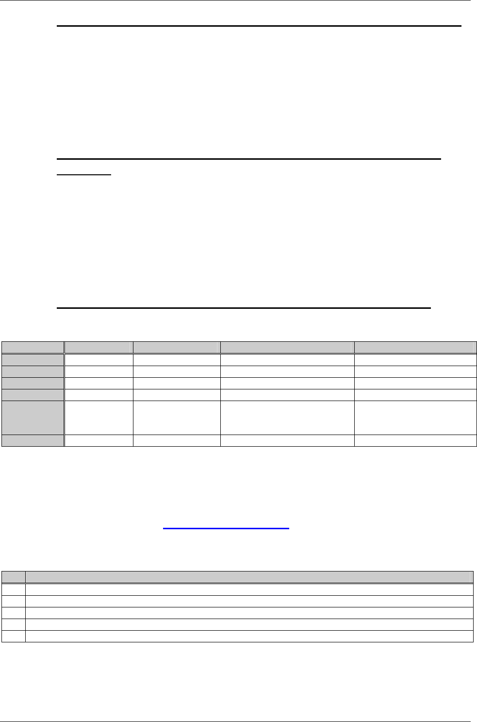
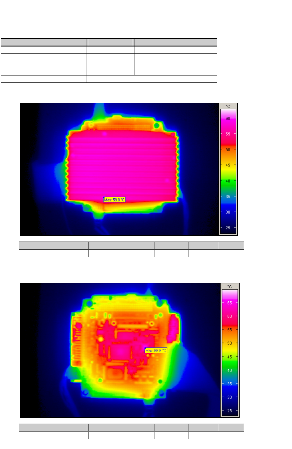
2.9. Thermoscan
Equipment:
Product Part Number Serial Number Version
MSM855 803010 46201010507 1.1
SM855-11P 1.1GHz 805161 45216110026 0.8
SM855-P378 1.4GHz 805164 45316410032 0.8
SODIMM DDR 1GB 870672 - -
Software Windows XP SP2 running desk top
MSM855-11P Top view
t [min] fCPU [MHz]
I [A] TSensor[°C]
TCPU[°C] THS[°C] P [W]
60 1100 3.65 65 69 63 18.6
MSM855-11P Bottom view:
t [min] fCPU [MHz]
I [A] TSensor[°C]
TCPU[°C] TKK[°C]
P [W]
60 1100 3.68 67 72 65 18.8
DIGITAL-LOGIC AG MSM855/HLV/B/B2 Detailed Manual V1.0A
34
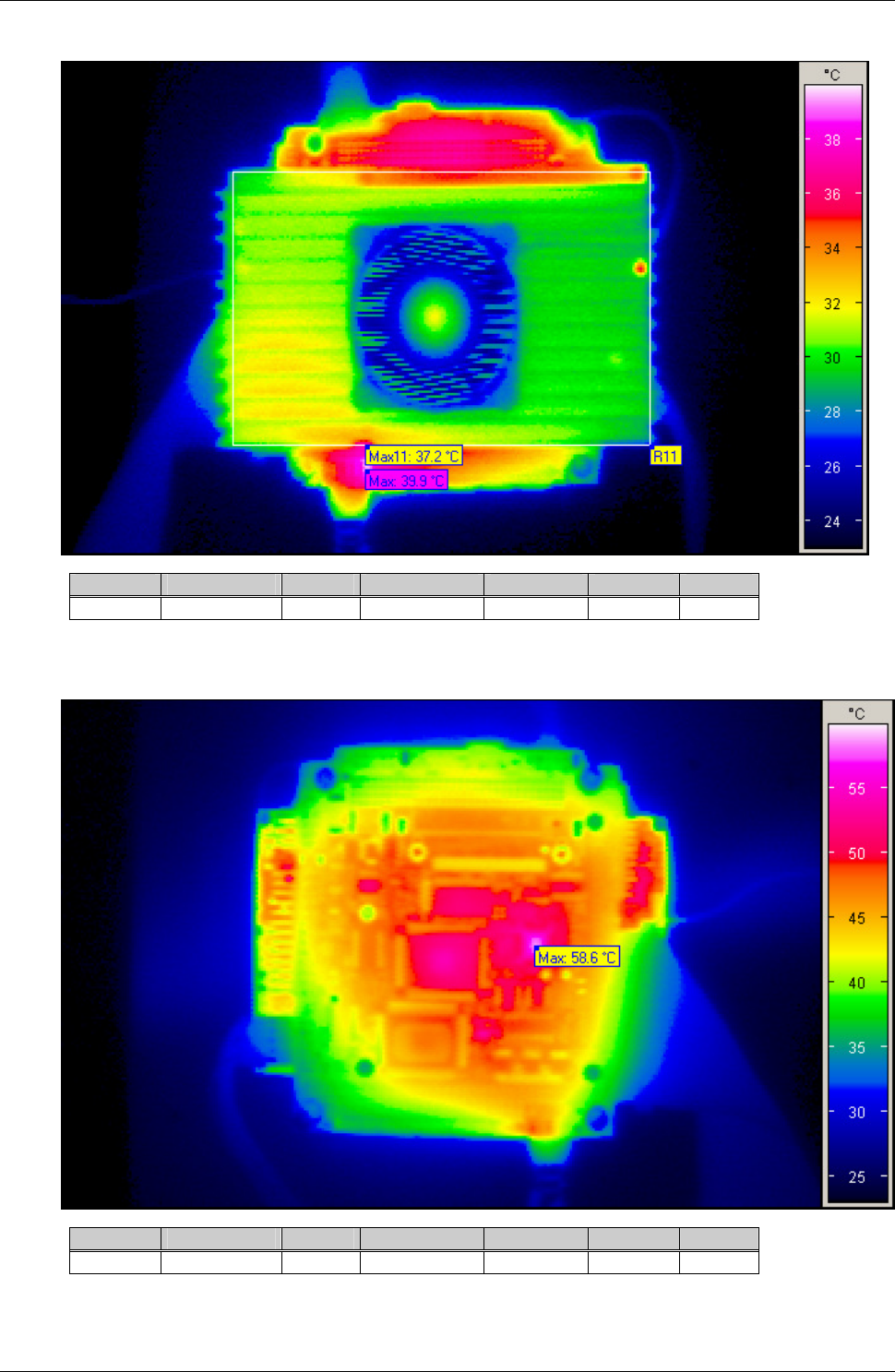
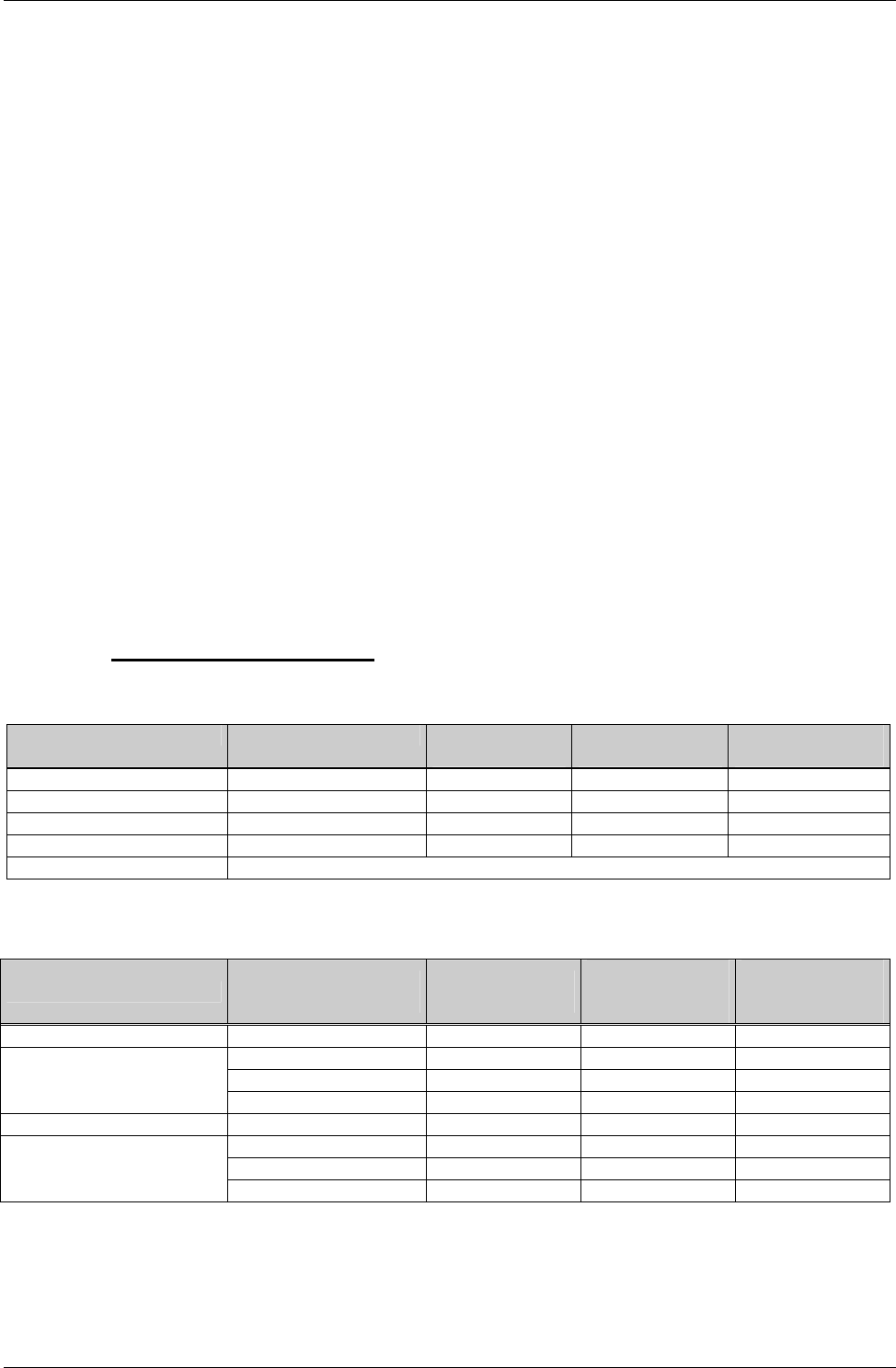
MSM855-738 Top view:
t [min] fCPU [MHz]
I [A] TSensor[°C]
TCPU[°C] THS[°C] P [W]
60 1400 3.58 42 47 32 18.3
MSM855-738 Bottom view:
t [min] fCPU [MHz]
I [A] TSensor[°C]
TCPU[°C] THS[°C] P [W]
60 1400 3.65 53 59 44 18.6

DIGITAL-LOGIC AG MSM855/HLV/B/B2 Detailed Manual V1.0A
35
2.10. High Frequency Radiation (to meet EN55022/EN61000)
Since the PC/104 CPU modules are very highly integrated embedded computers, peripheral lines are not
protected against radiation from the high frequency spectrum. To meet a typical EN55022 requirement, all
peripherals that go outside of the computer case must be externally filtered.
Typical signals that must be filtered:
Keyboard: KBCLK, KBDATA, VCC
Mouse: MSCLK, MSDATA, VCC
COM1/2/3/4: All serial signals must be filtered
LPT: All parallel signals must be filtered
CRT: Red, blue, green, hsynch and vsynch must be filtered
Typical signals that must not be filtered, since they are used internally:
IDE: Connected to the hard disk
Floppy: Connected to the floppy
LCD: Connected to the internal LCD
2.10.1. For Peripheral Cables:
Use a filtered version for all DSUB connectors. Select the filter specifications carefully. Place the filtered
DSUB connector directly on the front side and be sure that the shielding makes good contact with the case.
9pin DSUB connector from AMPHENOL: FCC17E09P 820pF
25pin DSUB connector from AMPHENOL: FCC17B25P 820pF
2.10.2. For Stack-Through Applications:
On each peripheral signal line that goes outside the computer case, place a serial inductivity followed by a
grounded capacitor of 100pF to 1000pF. In this case, no filtered connectors are needed. Place the filter
directly under or behind the onboard connector.
Serial Inductivity: TDK HF50ACB321611-T 100Mhz, 500mA, 1206 Case
Ground capacitor: Ceramic Capacitor with 1000pF
2.10.3. Power Supply:
Use a current-compensated dual inductor on the 5V supply.
For more information, please see Section 5.1.
DIGITAL-LOGIC AG MSM855/HLV/B/B2 Detailed Manual V1.0A
36
2.11. RTC Battery Lifetime
An AT compatible date/time clock is located within the chipset. The device also contains a CMOS static RAM
compatible with that in standard ATs. System configuration data is normally stored in the clock chip's CMOS
RAM in a manner consistent with the convention used in other AT compatible computers.
There are two ways to connect an external 3.6V lithium battery.
1. The most commonly used connection:
MSM855
The LAN-adaptor includes the LAN-transformer and the lithium battery. We recommend connecting
the battery to J29 , the universal LAN-Adaptor-Connector. The LAN-adaptor and the LAN-cable are
included.
MSM855B/B2
There is an onboard battery socket for a BR1225.
2. Alternative connection:
Keyboard connector J8 (pin8 = battery 3.6V input, pin7 = GND).
If the the battery is connected to J8, the J29 must not be used to connect the RTC-battery.
The battery-backed clock may be set during the boot process by using DIGITAL-LOGIC's setup.
2.11.1. Maxell ER3 (MSM855)
Battery Specifications Lowest Temp.
-40°C
Nominal Temp.
+20°C
Highest Temp.
+85°C
Manufacturer pbq
Type ER10280
Capacity versus Temp. 8uA 850mAh 910mAh 850mAh
Voltage versus Temp. 8uA 3.5V 3.6V Ca. 3.6V
Nominal Values 3.6V / 450mAh / -40°C...~+85°C
Information is taken from the datasheet of the pbq ER10280
Product Temperature
°C
Battery Voltage
V
VCC (+5V)
switched ON
µA
VCC (+5V)
switched off
µA
MSM855
+25°C 3.6 0.1 8
-40°C 3.5 0.1 8
Battery Current
+85°C 3.6 0.1 8
+25°C >10 years >5 years
-40°C >10 years >4 years
Battery Lifetime
+85°C >10 years ~3 years
DIGITAL-LOGIC AG MSM855/HLV/B/B2 Detailed Manual V1.0A
37
2.11.2. BR1225 (MSM855B/B2)
Battery Specifications Lowest Temp.
-30°C
Nominal Temp.
+20°C
Highest Temp.
+80°C
Manufacturer Various
Type BR1225
Capacity versus Temp. 7uA 35mAh 48mAh 50mAh
Voltage versus Temp. 7uA 2.6V 3V 3V
Nominal Values 3V / 48mAh / -30°C...~+80°C
Information taken from the datasheet of Panasonic BR1225
Product Temperature
°C
Battery Voltage
V
VCC (+5V)
switched ON
µA
VCC (+5V)
switched off
µA
MSM855B/B2
+25°C 3 0.1 7
-40°C 2.6 0.1 7
Battery Current
+85°C 3 0.1 7
+25°C >5 years ~280 days
-40°C >5 years ~210 days
Battery Lifetime
+85°C >5 years ~300 days
2.11.3. External Battery Assembly
If the customer wants to connect an external battery (check for the appropriate connector in Chapter 6),
some precautions must be taken:
Do not use a rechargeable battery – the battery is prohibited from charging.
The RTC device defines a voltage level of 2.0-3.6V, so use an external battery within this range
(inclusive of the diode which is already assembled onboard).

DIGITAL-LOGIC AG MSM855/HLV/B/B2 Detailed Manual V1.0A
38
3. CHIPSET DESCRIPTION
3.1. INTEL Processor Pentium-M
The Intel® Pentium® M processor is a high-performance, low-power mobile processor with several micro-
architectural enhancements over existing Intel mobile processors.
The following is a list of some of the key features on this processor:
Supports Intel® Architecture with Dynamic Execution
High-performance, low-power core
On-die, primary 32kByte instruction cache and 32kByte write-back data cache
On-die, 1/2MByte 2nd level cache with Advanced Transfer Cache Architecture
Advanced Branch Prediction and Data Prefetch Logic
Streaming SIMD Extensions 2 (SSE2)
400/533MHz, source-synchronous processor system bus
Advanced Power Management features including Enhanced Intel® SpeedStep® technology
Micro-FCPGA and Micro-FCBGA packaging technologies
The Intel Pentium M processor is manufactured on Intel’s advanced 0.13/0.09 micron process technology
with copper interconnect. The processor maintains support for MMX™ technology and Internet Streaming
SIMD instructions and full compatibility with IA-32 software. The high-performance core features architectural
innovations like Micro-op Fusion and Advanced Stack Management that reduce the number of micro-ops
handled by the processor. This results in more efficient scheduling and better performance at lower power.
The on-die 32kB Level 1 instruction and data caches and the 1MB Level 2 cache with Advanced Transfer
Cache Architecture enable significant performance improvement over existing mobile processors. The
processor also features a very advanced branch prediction architecture that significantly reduces the number
of mispredicted branches. The processor’s Data Prefetch Logic speculatively fetches data to the L2 cache
before an L1 cache requests occurs, resulting in reduced bus cycle penalties and improved performance.
The Streaming SIMD Extensions 2 (SSE2) enable break-through levels of performance in multimedia
applications including 3-D graphics, video decoding/encoding, and speech recognition. The new packed
double-precision floating-point instructions enhance performance for applications that require greater range
and precision, including scientific and engineering applications and advanced 3-D geometry techniques,
such as ray tracing.
The Intel Pentium M processor’s 400MHz processor system bus utilizes a split-transaction, deferred reply
protocol. The 400MHz processor system bus uses Source-Synchronous Transfer (SST) of address and data
to improve performance by transferring data four times per bus clock (4X data transfer rate, as in AGP 4X).
Along with the 4X data bus, the address bus can deliver addresses two times per bus clock and is referred to
as a “double-clocked” or 2X address bus. Working together, the 4X data bus and 2X address bus provide a
data bus bandwidth of up to 3.2GBytes/second. The processor system bus uses Advanced Gunning
Transceiver Logic (AGTL+) signal technology, a variant of GTL+ signalling technology with low power
enhancements.
Note: The term AGTL+ has been used for Assisted Gunning Transceiver Logic technology on other Intel
products.

DIGITAL-LOGIC AG MSM855/HLV/B/B2 Detailed Manual V1.0A
39
3.1.1. Introduction
The processor features Enhanced Intel SpeedStep technology, which enables real-time dynamic switching
between multiple voltage and frequency points instead of two points supported on previous versions of Intel
SpeedStep technology. This results in optimal performance without compromising low power. The processor
features the Auto Halt, Stop-Grant, Deep Sleep, and Deeper Sleep low-power states. The Intel Pentium M
processor utilizes socket-able Micro Flip-Chip Pin Grid Array (Micro-FCPGA) and surface mount Micro Flip-
Chip Ball Grid Array (Micro-FCBGA) package technology. The Micro-FCPGA package plugs into a 479-hole,
surface-mount, Zero Insertion Force (ZIF) socket, which is referred to as the mPGA479M socket.
This document includes specifications for the Intel Pentium M processor at Highest Frequency Mode (HFM)
core frequencies of 1.30, 1.40, 1.50, and 1.60GHz, the Low Voltage Intel Pentium M processor at HFM core
frequency of 1.10GHz and the Ultra Low Voltage Intel Pentium M processor at HFM core frequency of
900MHz.
3.1.2. Deep Sleep State
Deep Sleep state is a very low power state the processor can enter while maintaining context. Deep Sleep
state is entered by asserting the DPSLP# pin while in the Sleep state. BCLK may be stopped during the
Deep Sleep state for additional platform level power savings. BCLK stop/restart timings on Intel 855PM and
Intel 855GME chipset-based platforms are as follows:
Intel® Pentium® M Processor Datasheet 14
3.1.3. Low Power Features
Deep Sleep entry - DPSLP# and CPU_STP# are asserted simultaneously. The platform clock chip will
stop/tristate BCLK within 2 BCLKs +/- a few nanoseconds.
Deep Sleep exit - DPSLP# and CPU_STP# are deasserted simultaneously. The platform clock chip
will drive BCLK to differential DC levels within 2-3 ns and starts toggling BCLK 2-6 BCLK periods later.
To re-enter the Sleep state, the DPSLP# pin must be deasserted. BCLK can be re-started after DPSLP#
deassertion as described above. A period of 30 microseconds (to allow for PLL stabilization) must occur
before the processor can be considered to be in the Sleep state. Once in the Sleep state, the SLP# pin must
be deasserted to re-enter the Stop-Grant state. While in Deep Sleep state, the processor is incapable of
responding to snoop transactions or latching interrupt signals. No transitions of signals are allowed on the
system bus while the processor is in Deep Sleep state. Any transition on an input signal before the processor
has returned to Stop-Grant state will result in unpredictable behavior.
3.1.4. Deeper Sleep State
The Deeper Sleep state is the lowest power state the processor can enter. This state is functionally identical
to the Deep Sleep state but at a lower core voltage. The control signals to the voltage regulator to initiate a
transition to the Deeper Sleep state are provided on the platform. Please refer to the platform design guides
for details.

DIGITAL-LOGIC AG MSM855/HLV/B/B2 Detailed Manual V1.0A
40
3.1.5. Enhanced Intel® SpeedStep® Technology
(only available with Pentium-M CPUs, not with Celeron-M CPUs)
The Intel Pentium M processor features Enhanced Intel SpeedStep® technology. Unlike previous
implementations of Intel SpeedStep, this technology enables the processor to switch between multiple
frequency and voltage points instead of two. This enables superior performance with optimal power savings.
Switching between states is software controlled unlike previous implementations where the GHI# pin was
used to toggle between the two states.
The key features of Enhanced Intel SpeedStep technology are:
Multiple voltage/frequency operating points provide optimal performance at the lowest power.
Voltage/Frequency selection is software controlled by writing to processor MSR’s (Model Specific
Registers) thus eliminating chipset dependency.
o If the target frequency is higher than the current frequency, Vcc is ramped up by placing a new
value on the VID pins and the PLL then locks to the new frequency.
o If the target frequency is lower than the current frequency, the PLL locks to the new frequency
and the Vcc is changed through the VID pin mechanism.
o Software transitions are accepted at any time. If a previous transition is in progress, the new
transition is deferred until its completion.
The processor controls voltage ramp rates internally to ensure glitch free transitions.
Low transition latency and large number of transitions possible per second.
o Processor core (including L2 cache) is unavailable for up to 10 µs during the frequency transition
o The bus protocol (BNR# mechanism) is used to block snooping
Low Power Features:
No bus master arbiter disable required prior to transition and no processor cache flush necessary.
Improved Intel Thermal Monitor mode.
o When the on-die thermal sensor indicates that the die temperature is too high, the processor can
automatically perform a transition to a lower frequency/voltage specified in a software
programmable MSR.
o The processor waits for a fixed time period. If the die temperature is down to acceptable levels, an
up transition to the previous frequency/voltage point occurs.
o An interrupt is generated for the up and down Intel Thermal Monitor transitions enabling better
system level thermal management.
Enhancements:
Dynamic PSB Power Down
BPRI# control for address and control input buffers
Dynamic On Die Termination disabling
Low VCCP (I/O termination voltage) switching power at all times monitoring requirements in the
Deeper Sleep state.

DIGITAL-LOGIC AG MSM855/HLV/B/B2 Detailed Manual V1.0A
41
3.2. Graphic-Memory-Control Hub: INTEL 855GME
3.2.1. Processor Host Interface
The GMCH is optimized for the Intel Pentium M processor. Key features of the Intel Pentium M processor
system bus (PSB) are:
Source synchronous double-pumped address.
Source synchronous quad-pumped data.
System bus interrupt delivery.
Low voltage swing (Vtt = 1.05 V).
Dynamic Power Down (DPWR#) support.
GMCH supports a 64-B cache line size.
Support for a 400MHz system bus frequency. Dual processor is not supported.
Integrates AGTL+ termination resistors on all of the AGTL+ signals.
Supports 64bit host bus addressing allowing the CPU to access the entire 4GB of the GMCH
memory address space.
A 12-deep, In-Order queue to support up to twelve outstanding pipelined address requests on the
host bus.
Drives DPWR# signal to the processor, which can then disable its sense amplifiers.
Supports only one outstanding defer cycle at a time to any particular I/O interface.
Host initiated I/O cycles are positively decoded to the GMCH configuration space and subtractively
decoded to the Hub Interface
Host initiated memory cycles are positively decoded to DDR SDRAM.
Memory accesses initiated from the Hub Interface to DDR SDRAM will be snooped on the system
bus.
3.2.2. Intel 855GME GMCH Host Bus Error Checking
The Intel 855GME GMCH does not generate, nor check, parity on Data, Address/Request, and Response
signals on the PSB.
3.2.3. Intel 855GME GMCH System Memory Interface
The GMCH System Memory Controller directly supports the following:
One channel of PC1600/2100 SO-DIMM DDR SDRAM memory.
DDR SDRAM devices with densities of 128, 256 and 512MB technology.
Maximum System Memory with two, double-sided SO-DIMMs (four rows populated) supporting up
to 1GB system memory, and high density supporting up to 2GB system memory.
Variable page sizes of 2, 4, 8 and 16kB. Page size is individually selectable for every row and a
maximum of 16 pages may be opened simultaneously
The GMCH System Memory interface supports a thermal throttling scheme to selectively throttle reads
and/or writes. Throttling can be triggered either by the on-die thermal sensor, or by preset write bandwidth
limits. Read throttle can also be triggered by an external input pin. The memory controller logic supports
aggressive Dynamic Row Power Down features to help reduce power and supports Address and Control line
Tri-stating when DDR SDRAM is in an active power-down or in self-refresh state. The GMCH System
Memory architecture is optimized to maintain open pages (up to 16kB page size) across multiple rows. As a
result, up to 16 pages across four rows is supported. To complement this, the GMCH will tend to keep pages
open within rows, or will only close a single bank on a page miss. The GMCH supports only four bank
memory technologies.

DIGITAL-LOGIC AG MSM855/HLV/B/B2 Detailed Manual V1.0A
42
3.2.4. Intel 855GME GMCH Internal Graphics
The GMCH IGD provides a highly integrated graphics accelerator delivering high performance 2D, 3D, and
video capabilities. With its interfaces to UMA using a DVMT configuration, an analog display, a LVDS port,
and two digital display ports (e.g., flat panel), the GMCH can provide a complete graphics solution.
The GMCH also provides 2D hardware acceleration for block transfers of data (BLTs). The BLT engine
provides the ability to copy a source block of data to a destination and perform raster operations (e.g.,
ROP1, ROP2, and ROP3) on the data using a pattern, and/or another destination. Performing these
common tasks in hardware reduces CPU load, and thus improves performance. High bandwidth access to
data is provided through the System Memory interface. The GMCH uses Tiling architecture to increase
System Memory efficiency and thus maximize effective rendering bandwidth. The Intel 855GME GMCH also
improves 3D performance and quality with 3D Zone Rendering technology.
The GMCH has four display ports, one analog and three digital. These provide support for a progressive
scan analog monitor, a dedicated dual channel LVDS LCD panel, and two DVO devices. Each port can
transmit data according to one or more protocols. The DVO ports are connected to an external device that
converts one protocol to another. Examples of this are TV-out encoders, external DACs, LVDS transmitters,
and TMDS transmitters. Each display port has control signals that may be used to control, configure and/or
determine the capabilities of an external device. The data that is sent out the display port is selected from
one of the two possible sources, Pipe A or Pipe B.
3.2.5. Intel 855GME GMCH Analog Display Port
Intel 855GME GMCH has an integrated 350MHz, 24bit RAMDAC that can directly drive a progressive scan
analog monitor pixel resolution up to 2048x1600 at 85Hz refresh and up to 2048x1536 at 72Hz refresh. The
analog display port can be driven by Pipe A or Pipe B.
3.2.6. Intel 855GME GMCH Integrated DVO Ports
The DVO B/C interface is compliant with the DVI Specification 1.0. When combined with a DVI compliant
external device (e.g., TMDS Flat Panel Transmitter, TV-out encoder, etc.), the GMCH provides a high-speed
interface to a digital or analog display (e.g., flat panel, TV monitor, etc.).
The GMCH provides two DVO ports that are each capable of driving a 165MHz pixel clock at the DVO B or
DVO C interface. When DVO B and DVO C are combined into a single DVO port, then an effective pixel rate
of 330MHz can be achieved. The DVO B/C ports can be driven by Pipe A or Pipe B. If driven on Pipe B, then
the LVDS port must be disabled.
3.2.7. Hub Interface
A proprietary interconnect connects the GMCH to the ICH4-M. All communication between the GMCH and
the ICH4-M occurs over the Hub Interface 1.5. The Hub Interface runs at 66MHz (266MB/s).
3.2.8. Address Decode Policies
Host initiated I/O cycles are positively decoded to the GMCH configuration space and subtractively decoded
to the Hub Interface. Host initiated System Memory cycles are positively decoded to DDR SDRAM and are
again subtractively decoded to the Hub Interface if under 4GB. System Memory accesses from the Hub
Interface to DDR SDRAM will be snooped on the PSB.
DIGITAL-LOGIC AG MSM855/HLV/B/B2 Detailed Manual V1.0A
43
3.3. IO Control Hub Intel-ICH4M / ICH4
Features:
PCI Bus Interface Supports PCI Revision 2.2 Specification at 33MHz
133MB/sec maximum throughput
Supports up to six master devices on PCI
One PCI REQ/GNT pair can be given higher arbitration priority
(intended for external 1394 host controller)
Support for 44bit addressing on PCI using DAC protocol
Integrated LAN Controller WfM 2.0 and IEEE 802.3 compliant
LAN Connect Interface (LCI)
10/100Mbit/sec ethernet support
Integrated IDE Controller Supports "Native Mode” register and interrupts
Independent timing of up to 4 drives, with separate primary and
secondary IDE cable connections
Ultra ATA/100/66/33, BMIDE and PIO modes
Tri-state modes to enable swap bay
USB Includes three UHCI host controllers that support six external ports
New: Includes one EHCI high-speed USB 2.0 Host Controller that
supports all six ports
New: Supports a USB 2.0 high-speed debug port
Supports wake-up from sleeping states S1-S5
Supports legacy keyboard/mouse software
AC-Link for Audio CODECs Supports AC ’97 2.3
New: Third AC_SDATA_IN line for three codec support
New: Independent bus master logic for seven channels (PCM In/Out,
Mic 1 input, Mic 2 input, modem in/out, S/PDIF out)
Separate independent PCI functions for audio and modem
Support for up to six channels of PCM audio output (full AC3 decode)
Supports wake-up events
Interrupt Controller Support up to eight PCI interrupt pins
Supports PCI 2.2 message signaled interrupts
Two cascaded 82C59 with 15 interrupts
Integrated I/O APIC capability with 24 interrupts
Supports serial interrupt protocol
Supports processor system bus interrupt delivery
New: 1.5 V operation with 3.3 V I/O
5V tolerant buffers on IDE, PCI, USB overcurrent and legacy signals
Timers Based on 82C54 System timer, refresh request, speaker tone output
DIGITAL-LOGIC AG MSM855/HLV/B/B2 Detailed Manual V1.0A
44
Power Management Logic ACPI 2.0 compliant
ACPI-defined power states (C1-C2, S3-S5)
Supports Desktop S1 state (like C2 state, only STPCLK# active)
ACPI power management timer
PCI PME# support
SMI# generation
All registers readable/restorable for proper resume from 0V suspend
states
External Glue Integration Integrated pull-up, pull-down and series termination resistors on IDE,
processor interface
Integrated pull-down and series resistors on USB
Enhanced Hub Interface Buffers improve routing flexibility (Not available with all MemController Hubs)
Firmware Hub (FWH) Interface supports BIOS memory size up to 8MB
Low Pin Count (LPC) Interface Supports two Master/DMA devices
Enhanced DMA Controller Two cascaded 8237 DMA controllers
PCI DMA: Supports PC/PCI (Includes two PC/PCI REQ#/GNT# pairs)
Supports LPC DMA
Supports DMA collection buffer to provide Type-F DMA performance
for all DMA channels
Real-Time Clock 256Byte battery-backed CMOS RAM
System TCO Reduction Circuits Timers to generate SMI# and Reset upon detection of system hang
Timers to detect improper processor reset
Supports ability to disable external devices
SMBus New: Hardware packet error checking
New: Supports SMBus 2.0 Specification
Host interface allows processor to communicate via SMBus
Slave interface allows an external microcontroller to access system
resources
Compatible with most 2-wire components that are also I2C compatible
GPIO TTL, open-drain, inversion

DIGITAL-LOGIC AG MSM855/HLV/B/B2 Detailed Manual V1.0A
45
4. BUS SIGNALS
4.1. PC104 Bus
Note...
Not all of the signals are available on this board (please see Chapter 6 for a description of
the connectors).
AEN, output
Address Enable: used to degate the microprocessor and other devices from the I/O channel to allow
DMA transfers to take place. low = CPU Cycle, high = DMA Cycle
BALE, output
Address Latch Enable: provided by the bus controller and used on the system board to latch valid
addresses and memory decodes from the microprocessor. This signal is used so that devices on the
bus can latch LA17-23. The SA0-19 address lines latch internally according to this signal. BALE is
forced high during DMA cycles.
/DACK[0, 5-7], output
DMA Acknowledge: 0 to 3 and 5 to 7 are used to acknowledge DMA requests (DRQO through DRQ7).
They are active low. This signal indicates that the DMA operation can begin.
DRQ[0, 5-7], input
DMA Requests: 0 through 3 and 5 through 7 are asynchronous channel requests used by peripheral
devices and the I/O channel microprocessors to gain DMA service (or control of the system). A
request is generated by bringing a DRQ line to an active level. A DRQ line must be held high until the
corresponding DMA Request Acknowledge (DACK/) line goes active. DRQO through DRQ3 will
perform 8bit DMA transfers; DRQ5-7 are used for 16 accesses.
/IOCHCK, input
IOCHCK/: provides the system board with parity (error) information about memory or devices on the
I/O channel. low = parity error, high = normal operation
IOCHRDY, input
I/O Channel Ready: pulled low (not ready) by a memory or I/O device to lengthen I/O or memory
cycles. Any slow device using this line should drive it low immediately upon detecting its valid address
and a Read or Write command. Machine cycles are extended by an integral number of one clock cycle
(67 nanoseconds). This signal should be held in the range of 125-15600nS. low = wait, high =
normal operation
/IOCS16, input
I/O 16 Bit Chip Select: signals the system board that the present data transfer is a 16bit, 1 wait-state,
I/0 cycle. It is derived from an address decode. /IOCS16 is active low and should be driven with an
open collector (300 ohm pull-up) or tri-state driver capable of sinking 20mA. The signal is driven based
only on SA15-SAO (not /IOR or /IOW) when AEN is not asserted. In the 8bit I/O transfer, the default
transfers a 4 wait-state cycle.
/IOR, input/output
I/O Read instructs an I/O device to drive its data onto the data bus. It may be driven by the system
microprocessor or DMA controller, or by a microprocessor or DMA controller resident on the I/O
channel. This signal is active low.
/IOW, input/output
I/O Write: instructs an I/O device to read the data on the data bus. It may be driven by any
microprocessor or DMA controller in the system. This signal is active low.

DIGITAL-LOGIC AG MSM855/HLV/B/B2 Detailed Manual V1.0A
46
IRQ [10, 12, 14, 15], input
These signals are used to tell the microprocessor that an I/O device needs attention. An interrupt
request is generated when an IRQ line is raised from low to high. The line must be held high until
the microprocessor acknowledges the interrupt request.
/Master, input
This signal is used with a DRQ line to gain control of the system. A processor or DMA controller on the
I/0 channel may issue a DRQ to a DMA channel in cascade mode and receive a /DACK.
/MEMCS16, input
MEMCS16 Chip Select: signals the system board if the present data transfer is a 1 wait-state, 16bit,
memory cycle. It must be derived from the decode of LA17 through LA23. /MEMCS16 should be
driven with an open collector (300 ohm pull-up) or tri-state driver capable of sinking 20mA.
/MEMR, input/output
These signals instruct the memory devices to drive data onto the data bus. /MEMR is active on all
memory read cycles. /MEMR may be driven by any microprocessor or DMA controller in the system.
When a microprocessor on the I/0 channel wishes to drive /MEMR, it must have the address lines
valid on the bus for one system clock period before driving /MEMR active. These signals are active
low.
/MEMW, input/output
These signals instruct the memory devices to store the data present on the data bus. /MEMW is active
in all memory read cycles. /MEMW may be driven by any microprocessor or DMA controller in the
system. When a microprocessor on the I/O channel wishes to drive /MEMW, it must have the address
lines valid on the bus for one system clock period before driving /MEMW active. Both signals are
active low.
OSC, output
Oscillator (OSC): a high-speed clock with a 70 nanosecond period (14.31818 MHz). This signal is not
synchronous with the system clock. It has a 50% duty cycle. OSC starts 100µs after reset is inactive.
RESETDRV, output
Reset Drive: used to reset or initiate system logic at power-up time or during a low line-voltage outage.
This signal is active high. When the signal is active all adapters should turn off or tri-state all drivers
connected to the I/O channel. This signal is driven by the permanent Master.
/REFRESH, input/output
These signals are used to indicate a refresh cycle and can be driven by a microprocessor on the I/0
channel. These signals are active low.
SA0-SA19, LA17 - LA23 input/output
Address bits 0 through 19 are used to address memory and I/0 devices within the system. These 20
address lines, allow access of up to 1MBytes of memory. SAO through SA19 are gated on the system
bus when BALE is high and are latched on the falling edge of BALE. LA17 to LA23 are not latched and
addresses the full 16MByte range. These signals are generated by the microprocessors or DMA
controllers. They may also be driven by other microprocessor or DMA controllers that reside on the I/0
channel. The SA17-SA23 are always LA17-LA23 address timings for use with the MSCS16 signal.
This is advanced AT96 design. The timing is selectable with jumpers LAxx or SAxx.
/SBHE, input/output
Bus High Enable (system): indicates a transfer of data on the upper byte of the data bus, XD8 through
XD15. Sixteen-bit devices use /SBHE to condition data-bus buffers tied to XD8 through XD15.
SD[0-15], input/output
These signals provide bus bits 0 through 15 for the microprocessor, memory, and I/0 devices. D0 is
the least significant bit and D15 is the most significant bit. All 8bit devices on the I/O channel should
use D0 through D7 for communications to the microprocessor. The 16bit devices will use D0 through
D15. To support 8bit devices, the data on D8 through D15 will be gated to D0 through D7 during 8bit
transfers to these devices; 16bit microprocessor transfers to 8bit devices will be converted to two 8bit
transfers.
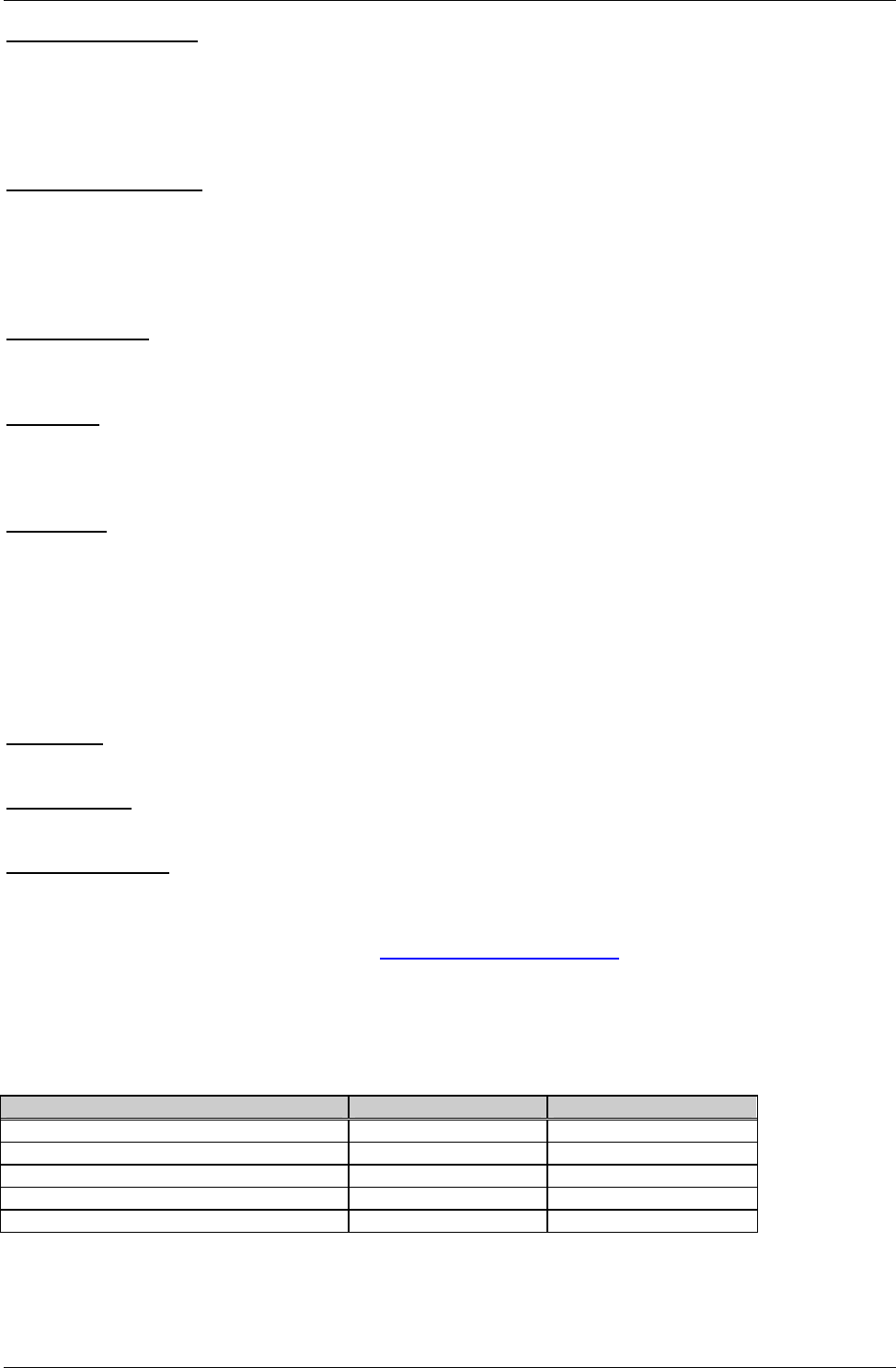
DIGITAL-LOGIC AG MSM855/HLV/B/B2 Detailed Manual V1.0A
47
/SMEMR, input/output
These signals instruct the memory devices to drive data onto the data bus for the first MByte. /SMEMR
is active on all memory read cycles. /SMEMR may be driven by any microprocessor or DMA controller
in the system. When a microprocessor on the I/0 channel wishes to drive /SMEMR, it must have the
address lines valid on the bus for one system clock period before driving /SMEMR active. The signal is
active low.
/SMEMW, input/output
These signals instruct the memory devices to store the data present on the data bus for the first
MByte. /SMEMW is active in all memory read cycles. /SMEMW may be driven by any microprocessor
or DMA controller in the system. When a microprocessor on the I/O channel wishes to drive /SMEMW,
it must have the address lines valid on the bus for one system clock period before driving /SMEMW
active. Both signals are active low.
SYSCLK, output
This is an 8MHz system clock. It is a synchronous microprocessor cycle clock with a cycle time of 167
nanoseconds. The clock has a 66% duty cycle. This signal should only be used for synchronization.
TC, output
Terminal Count: provides a pulse when the terminal count for any DMA channel is reached. The TC
completes a DMA-Transfer. This signal is expected by the onboard floppy disk controller. Do not use
this signal, because it is internally connected to the floppy controller.
/0WS, input
The Zero Wait State (/0WS) signal tells the microprocessor that it can complete the present bus cycle
without inserting any additional wait cycles. In order to run a memory cycle to a 16bit device without
wait cycles, /0WS is derived from an address decode gated with a Read or Write command. In order to
run a memory cycle to an 8bit device with a minimum of one-wait states, /OWS should be driven active
one system clock after the Read or Write command is active, gated with the address decode for the
device. Memory Read and Write commands to an 8bit device are active on the falling edge of the
system clock. /0WS is active low and should be driven with an open collector or tri-state driver
capable of sinking 20mA.
12V, +/- 5%
This signal is used only for the flat panel supply.
GROUND = 0V
This is used for the entire system.
VCC, +5V +/- 0.25V
This signal is used for logic and hard/floppy disk supply.
For further information about PC/104 and PC/104plus, please refer to the PC/104 Specification
Manual which is available on the internet: http://www.digitallogic.com (manuals).
4.2. Expansion Bus
The bus currents and maximum lengths are as follows:
Output Signals Voltage / Current Maximum Length
ISA-BUS (8MHz) 5.0V @ 8mA 50cm terminated
PCI-BUS (33MHz) 3.3V 30cm
LPC-Bus 3.3V 2mA 5cm
ATA-HD (33 Ohm termination onboard) 3.3V 20cm
USB 3.3V 6meter
for bus lengths > 10cm an AC-Bus termination is required.
DIGITAL-LOGIC AG MSM855/HLV/B/B2 Detailed Manual V1.0A
48
4.3. Addressing PCI Devices
4.3.1. MSM855/HLV
DEVICE IDSEL PIRQ #REG #GNT Remarks
Internal Chipset PCI Devices and Resources
GMCH Internal A / B / C / D - - PCI Bus 0
AGP Controller Internal A / B - - PCI Bus 0
Graphics Controller Internal A / B - - PCI Bus 0
ICH4_USB Controller Internal A / D / C / H - - PCI Bus 0
Func 0 = USB0 mapped to PIRQA
Func 1 = USB1 mapped to PIRQD
Func 2 = USB2 mapped to PIRQC
Func 7 = USB3 mapped to PIRQH
ICH4_PCI Controller Internal A / B / C / D - - PCI Bus 0
ICH4_LPC Controller C / B - - PCI Bus 0
IDE mapped to PIRQC
SMB mapped to PIRQB
AC97 Audio mapped to PIRQB
AC97 Modem mapped to PIRQB
Network AD24 E - - Internal chipset onboard device
External PCI Slots
PC/104+ Slot 1 AD20 E / F / G / H 0-4 0-4 PCI Bus 2
PC/104+ Slot 2 AD21 F / G / H / E 0-4 0-4 PCI Bus 2
PC/104+ Slot 3 AD22 G / H / E / F 0-4 0-4 PCI Bus 2
PC/104+ Slot 4 AD23 H / E / F / G 0-4 0-4 PCI Bus 2
Separate PCI Controller onboard:
DEVICE IDSEL PIRQ #REG #GNT Remarks
Firewire AD29 Not onboard
MiniPCI AD27 Not onboard
LAN2 AD26 Not onboard
LAN3 AD25 Not onboard
DIGITAL-LOGIC AG MSM855/HLV/B/B2 Detailed Manual V1.0A
49
4.3.2. MSM855B/B2:
DEVICE IDSEL PIRQ #REG #GNT Remarks
Internal Chipset PCI Devices and Resources
GMCH Internal A / B / C / D - - PCI Bus 0
AGP Controller Internal A / B - - PCI Bus 0
Graphics Controller Internal A / B - - PCI Bus 0
ICH4_USB Controller Internal A / D / C / H - - PCI Bus 0
Func 0 = USB0 mapped to PIRQA
Func 1 = USB1 mapped to PIRQD
Func 2 = USB2 mapped to PIRQC
Func 7 = USB3 mapped to PIRQH
ICH4_PCI Controller Internal A / B / C / D - - PCI Bus 0
ICH4_LPC Controller C / B - - PCI Bus 0
IDE mapped to PIRQC
SMB mapped to PIRQB
AC97 Audio mapped to PIRQB
AC97 Modem mapped to PIRQB
Network AD24 E - - Internal chipset onboard device
Network AD26 B 2 2 Only on MSM855B2
PCI to ISA Bridge AD22 3 3
External PCI Slots
PC/104+ Slot 1 AD20 E / F / G / H 0-4 0-4 PCI Bus 2
PC/104+ Slot 2 AD21 F / G / H / E 0-4 0-4 PCI Bus 2
PC/104+ Slot 3 NOT AVAILABLE
PC/104+ Slot 4 AD23 H / E / F / G 0-4 0-4 PCI Bus 2
Separate PCI Controller onboard:
DEVICE IDSEL PIRQ #REG #GNT Remarks
Firewire AD29 Not onboard
MiniPCI AD27 Not onboard
LAN2 AD26 Not onboard
LAN3 AD25 Not onboard
not available on MSM855B2
DIGITAL-LOGIC AG MSM855/HLV/B/B2 Detailed Manual V1.0A
50
5. DETAILED SYSTEM DESCRIPTION
This system's configuration is based on the ISA and PCI architecture. Read all information carefully as this is
very new computer technology.
5.1. Power Requirements
This product is an ATX-compatible PC and may only be provided through the power supply connector X8 or
X14/X15 with 5Volts if using the ATX- or ACPI features.
If you do not use the ATX- or ACPI features power may also be provided to the board through the PC104
BUS.
If using the MSMPS104 power supply from DIGITAL-LOGIC, then the ATX- or ACPI features are also
supported on the PC104 BUS.
Attention!
The Pentium-M is a very fast-changing, high-performance processor. The input current is a
direct function of the selected performance. The power supply must be capable of delivering the
maximum possible current (approximately 8Amp). Futhermore the supply must be able to
deliver the inrush current at power-on phase. The inrush current of 15Amp is very high but short
(only a few milliseconds).
We recommend the following power supplies:
1. PC104 PSU: MSMPS104 Part Nr.: 806032 – without UPS function
Part Nr.: 806030 – with UPS function
2. Laboratory PSU: EA-PS 1016-100 (0-16V/10A) http://www.elektroautomatik.de
3. AC/DC Switching PSU: TRACO TOL75-05 (5V/15A/75W) http://www.tracopower.com
5.1.1. Power Supply Cords
Power supply cords must be capable of fulfilling the voltage tolerance over the entire performance ratio. That
means not more than 100mV voltage drop at 8Ampere.
Since board V1.0, we recommend using the X14/X15 connectors to supply the board!
Note…
If you use connector X8: it is important to connect Pin2 and Pin8 of the power supply with +5Volt
and also connect Pin1 and Pin7 with ground. We recommend using a 4-wire cable, not longer
than 20cm, to the power supply.
DIGITAL-LOGIC AG MSM855/HLV/B/B2 Detailed Manual V1.0A
51
5.1.2. Typical Power Consumption
System with 2.5”-hard disk, CD-drive, PS2-KB&MS, 256MB-DDRAM, Pentium-M-1.6GHz CPU
Mode Power Consumption CPU-Performance Remarks
Booted under DOS 5V / 5Amp 1.6GHz No power management
Booted under XP and
idle in the desktop 5V / 2Amp Reduced to 0.6GHz ACPI power management
Stress test under XP 5V / 7Amp peak 1.6GHz and full
video performance
Standby from XP 5V / 0.8Amp CPU sleeps Not working
Average power 5V / 3Amp = 15Watt Office programs with more
than 80% idle time
Peripheral requirements
Device Quantity Power Consumption Remarks
USB 6 0.5A / 5V each Total 15W
Keyboard / Mouse 1 / 1 0.1A / 5V each Total 1W
HDD 80GB 1 4.7W (start-up) 2.3W (typical)
CDRW-DVD combo drive 1 0.9A / 5V 4.5W
5.1.3. Minimum Power-Off Time
Attention!
If the power is switched off, there must be a minimum 10 second off period.
All capacitors must be fully discharged before a new power-on is performed.
5.1.4. ATX–Compatible Power Function
Pin Signal Pin Signal
Pin 1 Main switch * Pin 2 GND
Pin 3 Power button **
* J16 default setting: closed by a jumper between Pins 1 and 2. If this jumper is closed until the main supply
comes up, the computer system starts by booting.
If you want to use a push button to start the system:
If this jumper is open until the main supply comes up, the board will not start. You must connect a
push button (main button) to Pin 1-2. After pushing the main button, the board will start. (If you press
the main button for more than 4 seconds, the power will switch off.)
** If you want to use the PWRBTN signal (i.e. in W2k or XP), you must connect another push button to Pins
2-3 of Jumper J16 in order to shut down the Windows OS at the push of the button.
Attention!
After the system is shut down using the power button; to restart, the main button (connected to Pins
1-2) must be used.
The PWRBTN signal is low active and internally pulled to 3.3Volt.
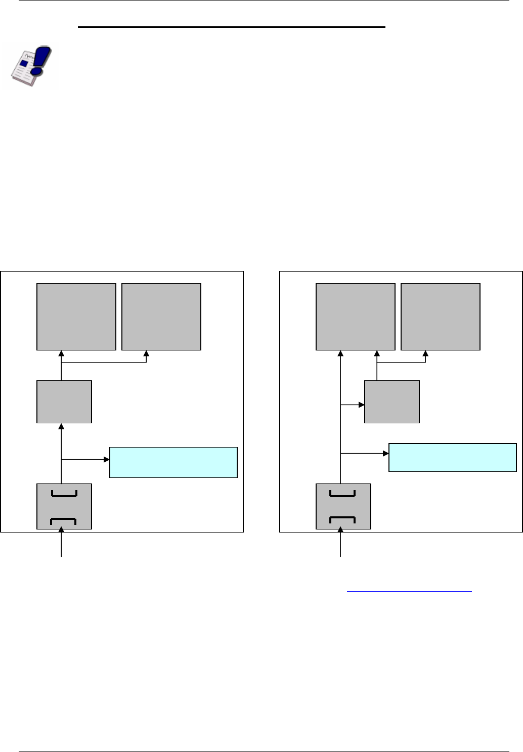
DIGITAL-LOGIC AG MSM855/HLV/B/B2 Detailed Manual V1.0A
52
5.1.5. MSM855-HLV-Input (High Level Voltage Input)
Note…
This product is only available with a separate part number (803012). For more information, please
contact your DIGITAL-LOGIC sales partner.
This product is also a MIL VG 96916-5-compatible PC. The board must be supplied through the power
supply connector or X14/X15 with 5-24Volt and 5V through the power pins of the PC104 bus.
The power dissipation of enclosed systems usually used for military mobile applications (24VDC supply) is
very critical depending on the system heat, especially in a harsh environment. For the thermal design power
(TDP) of the complete system, one must also be careful of the loss of DC/DC converters.
Starting with MSM855 Version 1.2, DIGITAL-LOGIC has solved this problem by providing HLV-Input which
allows the possibility of supplying the CPU board directly with 5-24V (approved to MIL VG 96916-5) on the
branch of the high power-consuming supply. For the additional peripheral 5V, a DC/DC converter with only
10W (instead 50-75W) can be used.
We recommend the following DC/DC converter: Eracom RP10S_DEW www.recom-international.de
PC104
MSM855
DC/DC
+5VDC / 50Watt
DC/DC
+24VDC /
60Watt
Other system components
+20..24VDC / 100Watt
PC104
Peripheral
3-6Watt loss
Typical configuration with a MSM855
PC104
MSM855
with
HLV-Input
DC/DC
+5VDC / 10Watt
DC/DC
+24VDC /
60Watt
+20..24VDC / 100Watt
PC104
Peripheral
0.5-1Watt loss
Optimized configuration with the MSM855-HLV-Input
Other system components
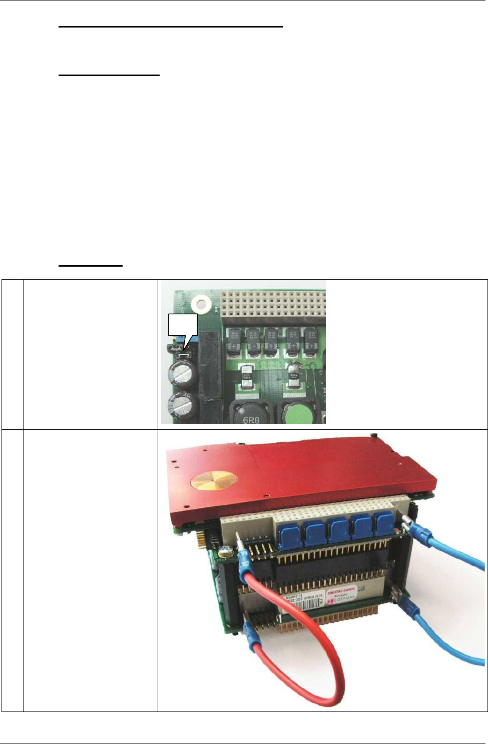
DIGITAL-LOGIC AG MSM855/HLV/B/B2 Detailed Manual V1.0A
53
5.1.6. MSMPS104 (PC104 power supply)
Below is the description of how to connect and configure the MSMPS104 to an MSM855.
5.1.6.1. Necessary Parts
MSMPS104, Part Nr. 806032
MSM855, Part Nr. 803010
MSM855-CK Cable Kit, Part Nor. 802032
Spacerkit-PC/104, Part Nr. 802050
or
Spacerkit-PC/104-Plus, Part Nr. 802051
(if option PC/104-Plus with connector long [Part Nr. 807006] is installed)
5.1.6.2. Procedure
1. Remove Jumper J2
2. Press the two 2x20 Pin and
the 2x32 Pin sockets in the
PC/104 connector of the
MSMPS104 board.
Press the 4x30 Pin socket in
the PC/104-Plus connector if
that option is installed.
Mount the four threaded
standoffs with four nuts on
the MSMPS104 board.
Place the MSM855 board on
the PC/104 connector of the
MSMPS104 and press it
down.
Fix the MSM855 board with
four screws on the threaded
standoffs.
Connect both boards
together with the cables
J2
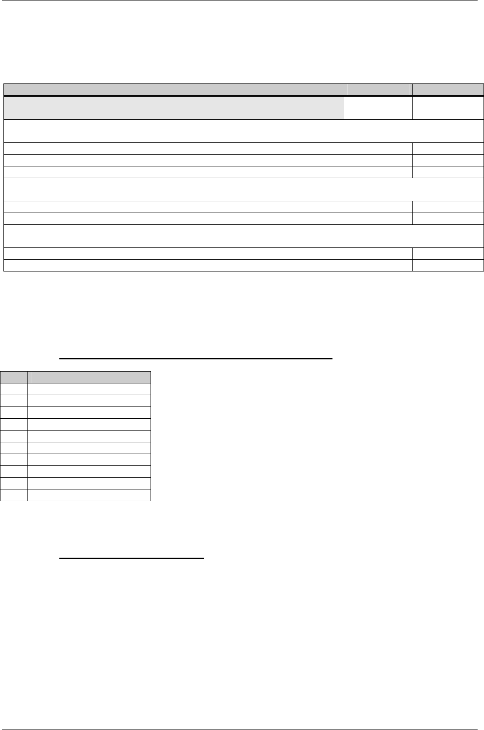
DIGITAL-LOGIC AG MSM855/HLV/B/B2 Detailed Manual V1.0A
54
5.2. Boot Time
System Boot-Times:
Definitions/Boot-Medium Quick Boot* Normal Boot
MSM855-1600MHz with RTC-backup battery
Memory 256MB shared 8MB for video
time [s] time [s]
From Floppy disk:
Boot from Setup-Disk1 MS-DOS v6.22 to "Starting MS-DOS“-Prompt 10 26
Boot from Setup-Disk1 MS-DOS v6.22 to "Welcome Setup Screen“-Prompt 30 45
Boot from "(Sys a:)-Disk“ to "A:/>“-Prompt 18 33
From Hard disk-Toshiba MK2110MAF:
Boot from Hard disk to "Starting MS-DOS“-Prompt 10 26
Boot from Hard disk to "Win2000: Windows-Login“-Prompt 80 95
From CompactFlash SunDisk SDCFB-64-101-00 64MB:
Boot from CF to "Starting MS-DOS“-Prompt 10 26
Boot from CF to "C:\>“-Prompt 13 29
5.3. Interfaces
5.3.1. AT Compatible Keyboard and PS/2 Mouse
Pin Signal
1 Speaker out
2 GND
3 External reset input
4 VCC
5 Keyboard Data
6 Keyboard Clock
7 GND
8 External Battery
9 Mouse Clock (PS/2)
10 Mouse Data (PS/2)
5.3.2. Line Printer Port LPT1
A standard bi-directional LPT port is integrated into the MICROSPACE PC.
Further information about these signals is available in numerous publications, including the IBM technical
reference manuals for the PC and AT computers and from other reference documents.
The current is: IOH = 12mA IOL = 24mA
The SMC 37C672 may be programmed via software commands. In the new BIOS version, this selection may
be controlled with the BIOS setup screen.
DIGITAL-LOGIC AG MSM855/HLV/B/B2 Detailed Manual V1.0A
55
5.3.3. Serial Ports COM1-COM2
The serial channels are fully compatible with 16C550 UARTS. COM1 is the primary serial port, and is
supported by the board's ROM-BIOS as the PC-DOS 'COM1' device. The secondary serial port is COM2; it
is supported as the 'COM2' device.
Standard: COM 1/2: SMC 37C672: 2 x 16C550 compatible serial interfaces
Serial Port Connectors COM1, COM2
Pin Signal Name Function in/out DB25 Pin
DB9 Pin
1 CD Data Carrier Detect in 8 1
2 DSR Data Set Ready in 6 6
3 RXD Receive Data in 3 2
4 RTS Request To Send out 4 7
5 TXD Transmit Data out 2 3
6 CTS Clear to Send in 5 8
7 DTR Data Terminal Ready out 20 4
8 RI Ring Indicator in 22 9
9 GND Signal Ground 7 5
10 nc
The serial port signals are compatible with the RS232C specifications.
5.3.4. Floppy Disk Interface
The onboard floppy disk controller and ROM-BIOS support one or two floppy disk drives in any of the
standard PC-DOS and MS-DOS formats shown in the table.
Supported Floppy Formats
Capacity Drive size Tracks Data rate DOS version
1.2MB 5-1/4" 80 500 KHz 3.0 - 6.22
720K 3-1/2" 80 250 KHz 3.2 - 6.22
1.4M 3-1/2" 80 500 KHz 3.3 - 6.22
Floppy Interface Configuration
The desired configuration of floppy drives (number and type) must be properly initialized in the board's
CMOS - configuration memory. This is generally done by using DEL or F2 at boot-up time.
Floppy Interface Connector
The table shows the pin-out and signal definitions of the board's floppy disk interface connector. It is
identical in pin-out to the floppy connector of a standard AT. Note that, as in a standard PC or AT, both
floppy drives are jumpered to the same drive select: as the 'second' drive. The drives are uniquely
selected as a result of a swapping of a group of seven wires (conductors 10-16) that must be in the
cable between the two drives. The seven-wire swap goes between the computer board and drive 'A';
the wires to drive 'B' are unswapped (or swapped a second time). The 26pin high density (1mm pitch
FCC) connector has only one drive and motor select. The onboard jumper defines the drive A: or B:.
Default is always A:.
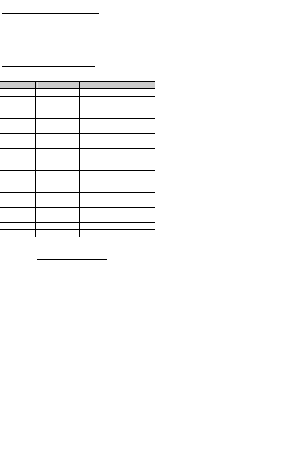
DIGITAL-LOGIC AG MSM855/HLV/B/B2 Detailed Manual V1.0A
56
Floppy Disk Interface Technology
Only CMOS drives are supported. This means that the termination resistors are 1 KOhm and 5 1/4“-
drives are not recommended (TTL interface).
The 26pin connector: FFC/FPC 0.3mm thick 1.0mm (0.039") pitch (MOLEX 52030 Serie)
Floppy Disk Interface Connector
FD26: Pin Signal Name Function in/out
1 VCC +5Volt
2 IDX Index Pulse in
3 VCC +5Volt
4 DS2 Drive Select 2 out
5 VCC +5Volt
6 DCHG Disk Change in
10 M02 Motor On 2 out
12 DIRC Direction Select out
14 STEP Step out
16 WD Write Data out
17 GND Signal grounds
18 WE Write Enable out
19 GND Signal grounds
20 TRKO Track 0 in
21 GND Signal grounds
22 WP Write Protect in
23 GND Signal grounds
24 RDD Read Data in
25 GND Signal grounds
26 HS Head Select out
5.3.5. Speaker Interface
One of the board's CPU devices provides the logic for a PC compatible speaker port. The speaker logic
signal is buffered by a transistor amplifier, and provides approximately 0.1Watt of audio power to an external
8 Ohm speaker. Connect the speaker between VCC and speaker output to have no quiescient current.
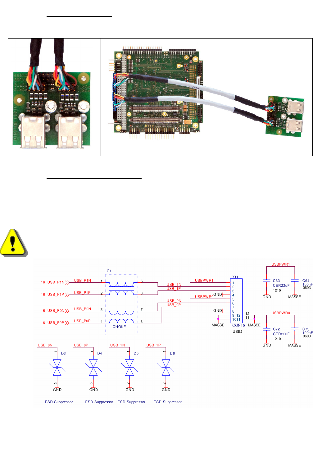
DIGITAL-LOGIC AG MSM855/HLV/B/B2 Detailed Manual V1.0A
57
5.3.6. 6 Port USB V2.0
USB cable connection
5.3.6.1. USB Interface Protection
Since the MSM855B and the MSM855 V1.3, this protection is implemented in the PCB
For all other versions of the MSM855:
The following is an example of a USB protection circuit (for two USB channels).
Attention!
This circuit must be implemented by the customer or it's possible the USB port or USB devices will
be destroyed (i.e., due to over voltage).
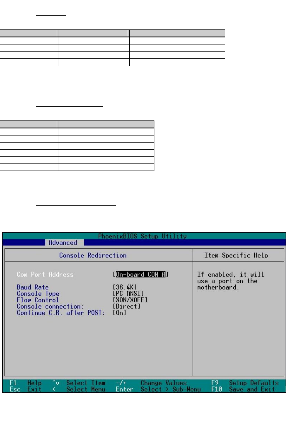
DIGITAL-LOGIC AG MSM855/HLV/B/B2 Detailed Manual V1.0A
58
5.3.6.2. Part List
Part Value Link
C 63, C72 22uF
C64, C73 100nF
D3, D4, D5, D6 PGB0010603MR http://www.littelfuse.com/
LC1 DLP31DN201ML4 http://www.murata.com/
X11 is a double USB connector; depending on the version, this connector may vary slightly.
5.3.6.3. Signal Description
Signal Description
USBPWR0 USB VCC 5V (Channel 1)
USBPWR1 USB VCC 5V (Channel 2)
USB_P0P USB Data + (Channel1)
USB_P0N USB Data - (Channel 1)
USB_P1P USB Data + (Channel 2)
USB_P1N USB Data - (Channel 2)
5.3.7. Console Redirection
Use a Null-modem cable to connect COM1 or COM 2 of the MSM855 to the COM1 (COM2) port of the host
PC. In the BIOS setup of the MSM855 you can configure the console redirection:
On the host PC you must start a terminal program (MSDOS or WINDOWS) which is able to show a minimum
of 25 lines.
DIGITAL-LOGIC AG MSM855/HLV/B/B2 Detailed Manual V1.0A
59
5.4. Controllers
5.4.1. Interrupt Controllers
An 8259A compatible interrupt controller, within the chipset, provides seven prioritized interrupt levels. Of
these, several are normally associated with the board's onboard device interfaces and controllers, and
several are available on the AT expansion bus.
Interrupt Sources Used Onboard
IRQ0 ROM-BIOS clock tick function, from timer 0 Yes
IRQ1 Keyboard controller output buffer full Yes
IRQ2 Used for cascade 2. 8259 Yes
IRQ3 COM2 serial port Yes
IRQ4 COM1 serial port Yes
IRQ5 LPT2 parallel printer (if present) No *
IRQ6 Floppy controller Yes
IRQ7 LPT1 parallel printer Yes
IRQ8 Battery backed clock Yes
IRQ9 Free for user No *
IRQ10 Free for user No *
IRQ11 Free for user No *
IRQ12 PS/2 mouse Yes
IRQ13 Math. coprocessor Yes
IRQ14 Hard disk IDE / SCSI Yes
IRQ15 Free for user No **
* Depends on the LAN configuration.
** IRQ 15 – if the optional CF is not assembled, then free for user.
5.5. Timers and Counters
5.5.1. Programmable Timers
An 8253 compatible timer/counter device is also included in the board's ASIC device. This device is utilized
in precisely the same manner as in a standard AT implementation. Each channel of the 8253 is driven by a
1.190MHz clock, derived from a 14.318MHz oscillator, which can be internally divided in order to provide a
variety of frequencies.
Timer 2 can also be used as a general purpose timer if the speaker function is not required.
Timer Assignment
Timer Function
0 ROM-BIOS clock tick (18.2Hz)
1 DRAM refresh request timing (15µs)
2 Speaker tone generation time base
5.5.2. Watchdog
The watchdog timer detects a system crash and performs a hardware reset. After power up, the watchdog is
always disabled as the BIOS does not send strobes to the watchdog. In case the user wants to take
advantage of the watchdog, the application must produce a strobe at least every 800ms. If no strobe occurs
within the 800ms, the watchdog resets the system. Please refer to the driver/software/BIOS manual
855_BIOS, the chapter on Driver Installation, LINUX SM855 Watchdog Support.
The watchdog function has been available since board Version 1.0.
DIGITAL-LOGIC AG MSM855/HLV/B/B2 Detailed Manual V1.0A
60
5.6. BIOS
5.6.1. BIOS History
Version
Date Status Modifications
1.2 Oct.03 Beta Basic version with APCI
1.5 Jan.04 Serial
release
Int15, IrDA, LPT, Standby functions, ACPI fixes
1.6 Feb.04
Boot from LAN, Wake up from LAN
1.7 Feb.04
IrDA fix, COM fix, Don't wait for F1 when error message
1.8 Mar.04
New video BIOS implemented, Int15 modified
1.9 Mar.04
Floppy boot / PXE boot enable
2.0 Apr.04 Keyboard init fix, new source code for Dothan implemented, new firmware hub
device support: SST49LF008A, ST50FW080
2.1 May.04
VGA BIOS 3276 implemented, PCI Table AD23 = RISER Card PIRQ H,E,F,G
2.2 Jun.04 New keyboard/mouse source code; CPU speed adjustable in the BIOS setup
2.3 Jul.04 LCD support is now adjustable in the BIOS setup; Dothan CPU support
added, ACPI fix for turn off COM1/2; LPT, Floppy and LAN under Windows
2.4 Aug.04
Ser_IRQ: newly configured to "continuous mode"
SuperI/O ACPI fix: If floppy, COM1/2 and LPT are disabled in the BIOS setup:
1. The devices are disabled and invisible in all OS
2. The free DMA are usable for other resources
PCI Configuration Menu under Advanced ( IRQ, DMA and UMB are
reservable for ISA).
2.5 Sep.04
Keyboard init fix
Dothan MicroCode update
HPET (High Performance Event Timer) enabled
Chassis Intruder detection removed
2.6 Oct.04
ATA100 support
PCITOISA Bridge support
Progress Bar
SMBattery Support (GPIO8 Interrupt)
VGA BIOS modified to enable CRT Monitor
2.7 Dec.04
SMBus optimized
2.8 Jan.05 Bugfix for Pod-Code 87h if CMOS invalid and Error during Boot
2.9 May.05
CPUID für Dothan Revision C0 (CPUID 6D8)
ACPI battery state, capacity and remaining time, ACPI negative temp. capture
corrected
3.01 Feb.06
CRTFIX: Added Setup Item IGD - CRTFix to set the LID Switch Status. If
closed, the Windows driver switches off LVDS and switches to CRT
Default Primary Video Adapter: Added this Setup item so it's possible to
select which graphics card is primary (internal or PCI)
ACPI Fix for No picture after standby
New VGA BIOS Version 1235, Add resolution 800x480 for LVDS Display
New PXE Boot Extension (removed RPL cause it was too large)
MemoryWindow set to 2MB for CardBus behind PCI Bridge
3.03 Mar.06
Final Video BIOS from Intel 1270
CH4/ICH4M universal BIOS
Fix for wrong SpeedStep Table if GV3
3.04 Mar.06
Fix for secondary IDE (was always Removable)
Corrected detection of Celeron without SpeedStep and TM1
3.05 Nov.06
Added USB 2.0 Legacy Support
Menu to select FullSpeed or HiSpeed
Disabling of USB2.0 Support fixed
3.09 Jul.07
PCI to ISA bridge
Attention! Please use the command line:
Phlash16.exe bios.wph /mode=3
to download a core BIOS greater than V3.05
DIGITAL-LOGIC AG MSM855/HLV/B/B2 Detailed Manual V1.0A
61
5.6.2. Core BIOS Download
5.6.2.1. Before downloading a BIOS
Please read through this section carefully and prepare for the download.
Make a bootable diskette which includes the following files:
DELEP855.EXE
phlash16.exe
core BIOS (SM855_xx_FLASHABL.ROM)
Rename the SM855_xx_FLASHABL.ROM file to bios.wph
To update a BIOS to a version greater than V3.05 you must use the following command line:
phlash16.exe bios.wph /mode=3
Important: Do not use boot disks created in a Windows operating system. If you do not have an MSDOS
6.22 disk available, you can download a boot disk from www.bootdisk.com.
NOTE…
Use SM855_xx_FLASHABL.ROM for downloading with the phlash16.exe.
The BIOS SM855_xx.cor is only usable by an external programmer.
Boot the DOS without config.sys and autoexec.bat press F5 while starting the DOS boot.
Disable the EMM386 or other memory managers in the CONFIG.SYS of your boot disk.
Make sure that the PHLASH16.EXE program and the BIOS to download are on the same path and
directory!
Check, where the PHLASH16.EXE is located, that the available disk space is larger than 64kB (for
safe storage).
Make sure the floppy disk not write-protected.
5.6.2.2. Start the download
1. Start the system with the bootable diskette. If you do not have a bootable diskette or floppy drive, you
can start in DOS mode by pressing the F5 key to disable autoexec.bat and config.sys.
2. Run DELEP855.EXE to clear the CMOS and the EEPROM
Attention!
If you do not run delep855.exe, the system will be destroyed during the BIOS upgrade!
3. Run phlash16.exe bios.wph /mode=3
4. If the BIOS download is finished you must power-off the system
5. Power-on the system and wait for the long “beep” signal
6. Power-off the system again
7. After powering the system on again, press F2 to enter setup; set the default values with F9; save and
leave setup with F10
8. Power-off the system
9. The download procedure is now finished.