Dialog Semiconductor SC14S DECT Module User Manual SC14CVMDECT SF01 V16
Dialog Semiconductor BV DECT Module SC14CVMDECT SF01 V16
Contents
- 1. user manual CVMDECT
- 2. user manual SPNODE
- 3. Rev_User Manual_68-2959-01_Bx_101217.pdf
user manual CVMDECT
© 2012 Dialog Semiconductor B.V. 1 www.dialog-semiconductor.com
SC14CVMDECT SF Cordless Voice Module
DATASHEET
General description
The SC14CVMDECT SF is a member of the Cordless
Module family with integrated radio transceiver and
baseband processor in a single package. It is designed
for hosted and embedded cordless voice and data
applications in the DECT frequency band. Its simple to
use API commands allow easy setup of a wireless link
between two or more nodes.
Features
nSupports EU-DECT (CAT-iq V2.0, v3.0 partly),
DECT6.0 for North America and Japan DECT
nETSI (EU-DECT) and FCC (DECT 6.0) certified
nJ-DECT pre-certified
nETSI 300 444 (DECT GAP) compliant
nUp to 6 Portable Parts or ULE devices registered per
fixed part
nUART interface to external host
nControllable via API command set
nSupports voice and data
nRF range: 1870 MHz to 1930 MHz
nReceiver sensitivity < -93 dBm
nTransmit power
• EU: 24 dBm: 1881MHz - 1897MHz
• USA: 20 dBm: 1921MH - 1928MHz
• JP: 23 dBm: 1895MHz - 1903MHz
nAntenna embedded, supports external antennas
nPower supply voltage: 2.1 V to 3.45 V
nSmall form factor (19.6 mm x 18.0 mm x 2.7 mm)
nContains both PP and FP functionality
nProgram memory available for custom software
nSupports both internal and external (hosted) applica-
tions
nOperating temperature range: -40 °C to +85 °C
Application examples
nCordless intercom
nCordless baby monitor
nWireless data applications up to 54 kbit/s
________________________________________________________________________________________________
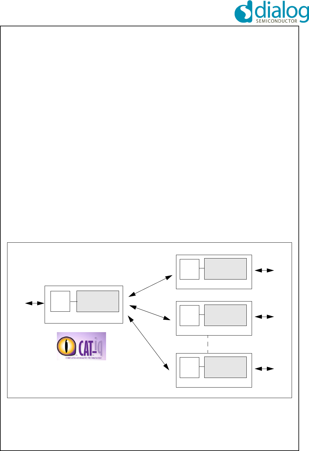
System diagram
SC14CVMDECT
Fixed Part
Data
Host
SC14CVMDECTHost
US/EU/JP*
DECT
Portable Part 0
SC14CVMDECTHost
Portable Part 1
SC14CVMDECTHost
Portable Part 5
Voice
Voice + data: 32 kbit/s + 1.6 kbit/s
Data: 54 kbit/s
* Only end-products
can be CAT-iq certified
*
Voice + data
Data
Voice + data
Data
Voice + data
Data
SC14CVMDECT SF
Cordless Voice Module
JULY 1, 2014 V1.6

SC14CVMDECT SF Cordless Voice Module
© 2012 Dialog Semiconductor B.V. 2 July 1, 2014 v1.6
Table of Contents
1.0 Connection diagram. . . . . . . . . . . . . . . . . . . . . . . . 4
1.1 PIN DESCRIPTION. . . . . . . . . . . . . . . . . . . . . . 5
2.0 Introduction . . . . . . . . . . . . . . . . . . . . . . . . . . . . . . 8
2.1 SCOPE . . . . . . . . . . . . . . . . . . . . . . . . . . . . . . . 8
2.2 REFERENCES . . . . . . . . . . . . . . . . . . . . . . . . . 8
2.3 GLOSSARY AND DEFINITIONS . . . . . . . . . . . 8
3.0 Cordless Voice Module functionality . . . . . . . . . 10
3.1 MODULE HARDWARE . . . . . . . . . . . . . . . . . . 10
3.2 SOFTWARE CONTROL . . . . . . . . . . . . . . . . . 10
3.3 DECT PROTOCOL STACK . . . . . . . . . . . . . . 10
3.4 PORTABLE PART CONFIGURATION . . . . . . 11
3.5 FIXED PART CONFIGURATION . . . . . . . . . . 11
3.6 VOICE COMMUNICATION . . . . . . . . . . . . . . . 12
3.7 LIGHT DATA APPLICATION . . . . . . . . . . . . . 12
3.8 LU10 DATA APPLICATION . . . . . . . . . . . . . . 12
3.9 GENERAL FEATURES . . . . . . . . . . . . . . . . . . 14
4.0 Functional description. . . . . . . . . . . . . . . . . . . . . 15
4.1 UART INTERFACE . . . . . . . . . . . . . . . . . . . . . 15
4.2 VES (VIRTUAL EEPROM STORAGE) . . . . . . 15
4.2.1 VES layout . . . . . . . . . . . . . . . . . . . . . . . 15
4.2.2 VES access by MCU . . . . . . . . . . . . . . . 15
4.3 AUDIO CONFIGURATIONS . . . . . . . . . . . . . . 15
4.3.1 Audio connection . . . . . . . . . . . . . . . . . . 16
4.4 AUDIO ROUTING . . . . . . . . . . . . . . . . . . . . . . 17
4.4.1 FP AUDIO ROUTING . . . . . . . . . . . . . . 17
4.4.2 FP audio level adjustment . . . . . . . . . . . 17
4.4.3 PP audio routing . . . . . . . . . . . . . . . . . . 17
4.4.4 PP audio codec adjustment . . . . . . . . . . 17
4.4.5 General audio adjustment . . . . . . . . . . . 17
4.4.6 PP volume . . . . . . . . . . . . . . . . . . . . . . . 17
4.4.7 PP audio equalization . . . . . . . . . . . . . . 17
4.5 PP AUDIO MODES . . . . . . . . . . . . . . . . . . . . . 19
4.5.1 Power management. . . . . . . . . . . . . . . . 19
4.5.2 Earpiece mode. . . . . . . . . . . . . . . . . . . . 20
4.5.3 Alert mode . . . . . . . . . . . . . . . . . . . . . . . 20
4.6 CALL HANDLING . . . . . . . . . . . . . . . . . . . . . . 20
4.6.1 FP to PP call . . . . . . . . . . . . . . . . . . . . . 20
4.6.2 PP to FP call . . . . . . . . . . . . . . . . . . . . . 20
4.6.3 Intercom . . . . . . . . . . . . . . . . . . . . . . . . . 20
4.6.4 Conference . . . . . . . . . . . . . . . . . . . . . . 20
4.6.5 Page call . . . . . . . . . . . . . . . . . . . . . . . . 20
4.7 TONE/MELODY HANDLING. . . . . . . . . . . . . . 20
4.8 DATE AND REAL-TIME CLOCK. . . . . . . . . . . 20
4.9 BATTERY MANAGEMENT . . . . . . . . . . . . . . . 21
4.10 PROTOCOL STACK . . . . . . . . . . . . . . . . . . 21
4.10.1 DECT TBR22 . . . . . . . . . . . . . . . . . . . . 21
4.10.2 Out-of-Range handling. . . . . . . . . . . . . 22
4.10.3 Preamble antenna diversity . . . . . . . . . 22
4.10.4 Broadcasting messages. . . . . . . . . . . . 22
4.10.5 IWU to IWU messaging . . . . . . . . . . . . 22
4.11 REGISTRATION . . . . . . . . . . . . . . . . . . . . . . 22
4.11.1 Handling product identities. . . . . . . . . . 22
4.11.2 Deregistration. . . . . . . . . . . . . . . . . . . . 23
4.12 PCM INTERFACE . . . . . . . . . . . . . . . . . . . . . 23
4.12.1 PCM Interface for FP . . . . . . . . . . . . . . 23
4.12.2 PCM_FSC frequency. . . . . . . . . . . . . . 23
4.12.3 Length of PCM_FSC . . . . . . . . . . . . . . 23
4.12.4 Start position of FSC . . . . . . . . . . . . . . 23
4.12.5 PCM clock frequency . . . . . . . . . . . . . . 23
4.12.6 PCM data mode . . . . . . . . . . . . . . . . . . 24
4.12.7 PCM Interface for PP. . . . . . . . . . . . . . 27
4.13 ANTENNA OPERATION . . . . . . . . . . . . . . . . 27
4.13.1 Internal antenna only . . . . . . . . . . . . . . 28
4.13.2 Internal and external antenna with FAD 28
5.0 CAT-iq . . . . . . . . . . . . . . . . . . . . . . . . . . . . . . . . . . 29
5.1 INTRODUCTION . . . . . . . . . . . . . . . . . . . . . . . 29
5.2 CAT-IQ PROFILE OVERVIEW . . . . . . . . . . . . 29
5.2.1 Supported main features . . . . . . . . . . . . 29
6.0 Specifications . . . . . . . . . . . . . . . . . . . . . . . . . . . . 30
6.1 GENERAL . . . . . . . . . . . . . . . . . . . . . . . . . . . . 30
6.2 ABSOLUTE MAXIMUM RATINGS . . . . . . . . . 30
6.3 OPERATING CONDITIONS . . . . . . . . . . . . . . 31
6.4 DIGITAL INPUT/OUTPUT PINS . . . . . . . . . . . 31
6.5 ANALOG FRONT END . . . . . . . . . . . . . . . . . . 32
6.6 BATTERY MANAGEMENT . . . . . . . . . . . . . . . 36
6.7 BASEBAND PART . . . . . . . . . . . . . . . . . . . . . 36
6.8 RADIO (RF) PART . . . . . . . . . . . . . . . . . . . . . 37
6.9 RF POWER SUPPLY . . . . . . . . . . . . . . . . . . . 38
6.10 RF CHANNEL FREQUENCIES. . . . . . . . . . . 39
7.0 Design guidelines. . . . . . . . . . . . . . . . . . . . . . . . . 40
7.1 APPLICATION SOFTWARE FOR PP . . . . . . 40
7.2 APPLICATION SOFTWARE FOR FP . . . . . . 40
7.3 HARDWARE DESIGN GUIDELINES . . . . . . . 40
7.3.1 Circuit design guidelines . . . . . . . . . . . . 40
7.3.2 PCB Design Guidelines . . . . . . . . . . . . . 41
7.4 MODULE PLACEMENT ON THE MAIN BOARD

SC14CVMDECT SF Cordless Voice Module
© 2012 Dialog Semiconductor B.V. 3 July 1, 2014 v1.6
Table of Contents
42
7.5 PATTERN FOR PIN 79 ON THE MAIN BOARD.
42
7.6 PRECAUTIONS REGARDING UNINTENDED
COUPLING . . . . . . . . . . . . . . . . . . . . . . . . . . . 42
8.0 Example Application Diagram. . . . . . . . . . . . . . . 43
9.0 Notices to OEM. . . . . . . . . . . . . . . . . . . . . . . . . . . 44
9.1 FCC REQUIREMENTS REGARDING THE END
PRODUCT AND THE END USER. . . . . . . . . . 44
9.2 IC REQUIREMENTS REGARDING THE END
PRODUCT AND THE END USER . . . . . . . . . 44
9.3 PRECAUTIONS REGARDING UNINTENDED
COUPLING . . . . . . . . . . . . . . . . . . . . . . . . . . . 45
9.4 END APPLICATION APPROVAL . . . . . . . . . . 45
9.5 SAFETY REQUIREMENTS . . . . . . . . . . . . . . 45
10.0 Package information . . . . . . . . . . . . . . . . . . . . . 46
10.1 SOLDERING PROFILE . . . . . . . . . . . . . . . . . 46
10.2 MOISTURE SENSITIVITY LEVEL (MSL) . . . 46
10.3 COPPER PAD, SOLDER OPENING AND
STENCIL . . . . . . . . . . . . . . . . . . . . . . . . . . . . . 47
10.4 MECHANICAL DIMENSIONS . . . . . . . . . . . . 49
11.0 Revision history . . . . . . . . . . . . . . . . . . . . . . . . . 50
SC14CVMDECT SF Cordless Voice Module
© 2012 Dialog Semiconductor B.V. 4 July 1, 2014 v1.6
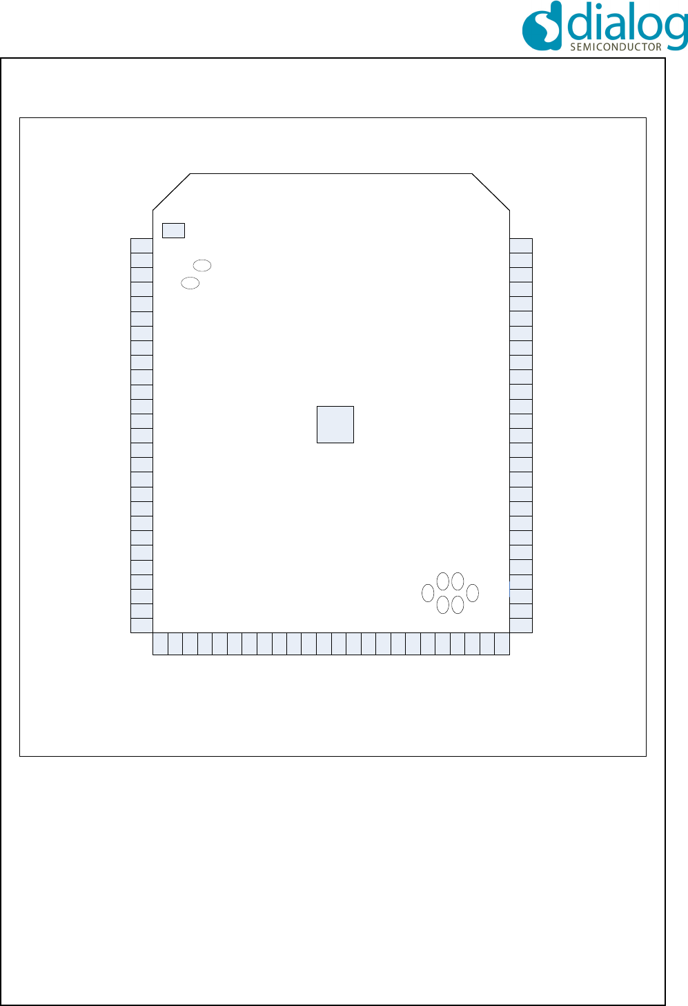
1.0 Connection diagram
Figure 1 Connection diagram (top view, leads face down)
Order numbers:
SC14CVMDECT SF01T (tray, MPQ = 600 pcs) up to 6 PPs can be registered.
1
23
22
21
20
19
18
17
16
15
14
13
12
11
10
9
8
7
6
5
4
3
2
27
49
48
47
46
45
44
43
42
41
40
39
38
37
36
35
34
33
32
31
30
29
28
26
25
24
72
50
51
52
53
54
55
56
57
58
59
60
61
62
63
64
65
66
67
68
69
70
71
79
80
GND
PARADET/P3[4]
P2[0]/ECZ1/PWM0/LED3
GND
TP1
RINGOUT/RINGING/P3[5]
GND
RFP0
P0
GND
GND
ADC0/P3[3]
LSRn/LINEOUT/AGND
LSRp/LINEOUT/AGND
VREFm
MICn/CIDOUT
MICp/CIDINn
VREFp
MICh/LINEIN
CIDINp/P3[2]
RINGp/P3[7]
RINGn/P3[6]
DC_I
DC_SENSE
SOCn
SOCp
ADC1/INT0/P1[0]
DC_CTRL
VDDE/RDI/INT5/P1[5]
ULP_PORT
ULP_XTAL
PON/P1[6]
CP_VOUT1
GND
DP0/PAOUTn/P3[0]
VDDPA
DP1/PAOUTp/P3[1]
CHARGE/P1[7]
CHARGE_CTRL
VBATSW
VBATIN
VBATIN
VDDOUT
GND
SIO/INT3/P1[3]
TDOD/INT4/P1[4]
BXTAL/INT7/P2[7]
SK/INT2/P1[2]
LE/INT1/P1[1]
P0[7]/PWM1SPI_DI
P0[6]/SPI_DO
GND
WTF_IN/P2[6]
P0[4]/SPI_EN
P0[3]/SCL2/URX2
P0[5]/SPI_CLK
P0[2]/SDA2/UTX2
P0[1]/PWM0/URX
P0[0]/UTX
GND
RSTn
JTAG
SF/P2[5]/PCM_FSC
DP3/P2[4]/SCL1/PCM_DO
DP2/P2[3]/SDA1/PCM_DI
CLK100/P2[2]/PCM_CLK
P2[1]/ECZ2/PWM1/LED4
RFP0n
P0n
RF1
GND
RF0
GND
GND
GND
GND
GND
78
77
76
75
74
73
GND
GND
GND
81
82
83
84
87
88
85
86
SC14CVMDECT SF Cordless Voice Module
© 2012 Dialog Semiconductor B.V. 5 July 1, 2014 v1.6
1.1 PIN DESCRIPTION
Table 1: Pin description
Pin
Module
Pin name
(Note 1)
In/
Out
Iout
Drive
(mA)
Reset
State
(Note 2)
Description
1GND - - -Ground
2 P0 O 8 Hi-Z Control port for FAD. See 4.13
3 RFP0 O 8 Hi-Z Control port for FAD. See 4.13
4 P0n O 8 Hi-Z Control port for FAD. See 4.13
5 RFP0n O 8 Hi-Z Control port for FAD. See 4.13
6GND - - -Ground
7 VREFp O - I Positive microphone supply voltage
8 MICp I - I Positive microphone input
9 MICn I - I Negative handset microphone input
10 MICh I - I Headset microphone input with fixed input protection
11 VREFm - - - Negative microphone reference (star point), connect to GND.
12 LSRp O - O Positive loudspeaker output
13 LSRn O - O Negative loudspeaker output
14 GND - - - Ground
15 P3[3] IO 8 I I/O Port
16 P1[0] IO 2 I-PU I/O Port
17 SOCp I - I Battery state of charge positive input.
Connect to GND if not used. See 4.9
18 SOCn I - I Battery state of charge negative input. Star point connected to the
SOC resistor. Connect to GND if not used. See 4.9
19 DC_SENSE I I Voltage sense input. Connect to GND if not used.
20 DC_I I I Current sense input of DC/DC converter. Connect to GND if not
used
21 DC_CTRL O 2 O-0 Switching clock for the DC/DC converter.
22 CHARGE_CTRL O 1 O-0 Charge control pin.
Leave unconnected if not used. See 4.9
23 CHARGE I - I-PD
(270k
fixed
pull-
down)
Charger connected indication. Switches on the device if voltage >
1.5 V. Must be connected to charger via resistor R >
(Vcharger_max-3 V)/10 mA (round to next largest value in range).
See 4.9
24 PAOUTp IO 500 O-0 (5k
fixed
pull-
down)
CLASSD loudspeaker positive outputs
25 VDDPA I - - CLASSD Audio Amplifier supply voltage up to 3.45 V.
GND or leave unconnected if CLASSD Audio Amplifier is not used.
26 CP_VOUT1 O - I Charge Pump Output 1.
A capacitor of 1 F to GND is internally connected to this pin.
27 PAOUTn IO 500 O-0 (5k
fixed
pull-
down)
CLASSD loudspeaker positive output
SC14CVMDECT SF Cordless Voice Module
© 2012 Dialog Semiconductor B.V. 6 July 1, 2014 v1.6
28 GND - - - Ground
29 PON I - I (270k
fixed
pull-
down)
Power on, Switches on the device if Voltage > 1.5 V.
May be directly connected to VBAT, also with Li-Ion batteries.
After startup the software takes over then PON pin to keep the
device on after which the PON pin may be released.
30 ULP_XTAL I - I 32.768 kHz XTAL clock input. Connect to GND if not used. (Note 3)
31 ULP_PORT I - I Ultra Low Power Port Pin. Connect to GND if not used. (Note 3)
32 P2[7] IO 8 I-PU I/O port
33 P1[5] IO 8 O-1 I/O Port
34 P1[4] IO 1/2 I-PD I/O port
35 P1[3] IO 1/2 I-PD I/O Port
36 P1[2] IO 2 I-PD I/O Port
37 P1[1] IO 2 I-PU I/O Port
38 GND - - - Ground
39 P2[6] IO 2 I-PU I/O port
40 P0[7] / SPI_DI IO 8 I-PU I/O Port
SPI Data Input
41 P0[6] / SPI_DO IO 8 I-PU I/O Port
SPI Data Out
42 P0[5] / SPI_CLK IO 8 I-PU I/O Port
SPI Clock
43 P0[4] / SPI_EN IO 8 I-PU I/O port
SPI_EN: Active low.
44 P0[3] / SCL2 /
URX2
IO 8 I-PU I/O port
Access bus clock, UART Serial In.
45 GND - - - Ground
46 P0[2] / SDA2 /
UTX2
IO 8 I-PU I/O port
Access bus data, UART Serial Out.
47 P0[1] / URX IO 8 I-PD
(10k)
I/O port
UART Serial In
48 P0[0] / UTX O 8 I-PU I/O Port
UART Serial Out
49 GND - - - Ground
50 GND - - - Ground
51 GND - - - Ground
52 RSTn I 1 I-PU
(200k
pull-up)
Active low Reset input with Schmitt-trigger input, open-drain output
and pull up resistor to internal VDD. Input may not exceed 2.0 V. An
internal capacitor of 47 nF is mounted on this pin.
53 JTAG IO 8 I-PU JTAG-SDI+; one wire Debug interface with open-drain.
Requires external 1 k pull-up to VDD.
54 P2[5]/PCM_FSC IO 8 I-PU I/O Port
PCM_FSC: PCM Frame Sync
55 P2[4]/SCL1/
PCM_DO
IO 8 I-PU I/O port
SCL1; I2C clock
PCM_DO: PCM Data output
Table 1: Pin description (Continued)
Pin
Module
Pin name
(Note 1)
In/
Out
Iout
Drive
(mA)
Reset
State
(Note 2)
Description
SC14CVMDECT SF Cordless Voice Module
© 2012 Dialog Semiconductor B.V. 7 July 1, 2014 v1.6
Note 1: “NC” means: leave unconnected.
“GND” means internally connected to the module ground plane. Every GND pin should be connected to the main PCB.ground plane.
Note 2: All digital inputs have Schmitt trigger inputs. After reset all I/Os are set to input and all pull-up or pull-down resistors are enabled unless oth-
erwise specified.
PU = Pull-up resistor enabled, PD = Pull-down resistor enabled, I = input,
O = output, Hi-Z = high impedance, 1 = logic HIGH level, 0 = logic LOW level
Refer also to Px_DIR_REGs for INPUT/OUTPUT and Pull-up/Pull-down configurations
Note 3: All ULP pins use snap-back devices as ESD protection, which (when triggered) have a holding voltage below the typical battery voltage.
This means that the snap-back device of a ULP pin may remain conductive, when triggered while the pin is directly connected to the battery
voltage. If any of the ULP pins are directly or indirectly electrically accessible on the outside of the application, system level ESD precau-
tions must be taken to ensure that the snap-back device is not triggered while in active mode, to prevent the chip from being damaged.
56 P2[3]/SDA1 /
PCM_DI
IO 8 I-PU I/O Port
SDA1: I2C Data
PCM_DI: PCM Data input
57 P2[2]/PCM_CLK I/O 8 I-PD I/O Port
PCM_CLK: PCM clock input/output
58 P2[1] / PWM1 /
LED4
IO 8 I I/O Port
PWM1: Pulse Width Modulation output
LED4: 2.5 mA/5 mA LED current sink
59 P2[0]/ PWM0 /
LED3
IO 8 I I/O Port
PWM0: -
LED3: 2.5 mA/5 mA LED current sink
60 GND - - - Ground
61 VDDOUT - - - Test purpose only. Must be left unconnected.
62 VBATSW Test purpose only. Must be left unconnected.
63 VBATIN I - - Main supply voltage < 3.45 V.
64 VBATIN I - - Main supply voltage < 3.45 V.
65 P3[2] IO 8 I I/O Port
66 P3[7] IO 4 I I/O Port
67 P3[6] IO 4 I I/O Port
68 P3[5] IO 4 I I/O Port
69 P3[4] IO 8 I I/O Port
70 GND - - - Ground
71 GND - - - Ground
72 GND - - - Ground
73 RF1 - - - RF signal for external antenna. See 4.13
74 GND - - - Ground
75 RF0 - - - RF signal for external antenna. See 4.13
76 GND - - - Ground
77 GND - - - Ground
78 GND - - - Ground
79 TP1 - - - Tuning point for internal antenna. Follow instructions of Section 7.5.
80 GND - - - Ground
81-88 TP2 to TP9 NC Must be left unconnected. See section 7.3.2 and Figure 36.
Table 1: Pin description (Continued)
Pin
Module
Pin name
(Note 1)
In/
Out
Iout
Drive
(mA)
Reset
State
(Note 2)
Description

SC14CVMDECT SF Cordless Voice Module
© 2012 Dialog Semiconductor B.V. 8 July 1, 2014 v1.6
2.0 Introduction
2.1 SCOPE
The SC14CVMDECT SF is a programmable DECT
module for voice and data services. The internal soft-
ware stack receives commands and data from the
application, for instance to set up a link to other mod-
ules. The application software can be implemented on
the module itself or on an external host processor. The
internal FLASH provides user space where custom
applications can be located.
The module converts analog signals to a digital stream,
compresses/decompresses them according to the
DECT standards and transmits/receives them over the
air interface. The DECT protocol stack in each module
supports both PP and FP functionality.
The embedded software running on the internal micro-
controller (CR16) supports all protocol layers up to the
network layer. The module can be controlled by soft-
ware running on the internal controller as well as from
an external controller via the UART.
2.2 REFERENCES
1. CVM FP API Documentation package
2. CVM PP API Documentation package
3. Athena Eclipse User Manual, v1.02, Dialog
Semiconductor, Cordless Software + Tools
4. SC14CVMDECT EEPROM (VES) MAP
5. AN-D-174, SC14480 Battery Management;
using the State of Charge function, Dialog Sem-
iconductor, Application Note
6. AN-D-204, RF settings in Natalie, Dialog Semi-
conductor, Application note
7. AN-D-211, SC14CVMDECT External antenna
design guidelines, Dialog Semiconductor, Appli-
cation note
2.3 GLOSSARY AND DEFINITIONS
AFE Analog Front End
API Application Programming Interface
software between the MCU and
SC14CVMDECT SF
Baby monitor Same as intercom but optionally voice
activated
CAT-iq Cordless Advanced Technology, Internet
and Quality
Codec Coder and Decoder converts analog
signals to digital signals and vice versa.
Conference Same as intercom, but including an
external party.
CRC Cyclic Redundancy Check
CVM Cordless Voice Module
DECT Digital Enhanced Cordless Telephone
DSP Digital Signal Processor
EMC Equipment Manufacturer’s Code
ESD ElectroStatic Discharge
FAD Fast Antenna Diversity
FP Fixed Part
GAP General Access Profile (DECT)
GFSK Gaussian Frequency Shift Keying
Inband tones Tones played by the application itself
and not from external e.g. line.
Intercom Internal call between FP and one or
more PPs
IPEI International Portable Equipment Identity
(please refer to ETSI EN 300 175-6)
IWU InterWorking Unit (please refer to ETSI
EN 300 175-1)
LCD Liquid Crystal Display
LDO Low Drop Out (regulator)
LDR Low Data Rate
MCU Micro Controller Unit
MMI Man Machine Interface (keypad, LCD,
buzzer, microphone, earpiece, speaker,
headset)
NSMD Non Solder Mask Defined (pad)
NTP Normal Transmitted Power
PAEC Perceptual Acoustic Echo Canceller
PC Personal Computer, IBM compatible
PCB Printed Circuit Board without
components
PP Portable Part
PSTN Public Switched Telephone Network
POTS Plain Old Telephone System
RF Radio Frequency
RFPI Radio Fixed Part Identity (please refer to
ETSI EN 300 175-6)
RLR Receive Loudness Rating
RSSI Radio Signal Strength Indication (please
refer to ETSI EN 300 175-1)
Sidetone Feedback of microphone signal to
earpiece.
SLR Sending Loudness Rating
SPI Serial Peripheral Interface Bus
UART Universal Asynchronous Receiver and
Transmitter
ULE Ultra Low Energy
VAD Voice Activity Detection

SC14CVMDECT SF Cordless Voice Module
© 2012 Dialog Semiconductor B.V. 9 July 1, 2014 v1.6
VES Virtual EEPROM Storage
Walkie Talkie Call between two PPs without an FP
SC14CVMDECT SF Cordless Voice Module
© 2012 Dialog Semiconductor B.V. 10 July 1, 2014 v1.6
3.0 Cordless Voice Module function-
ality
This section describes the key functions and features
supported by the SC14CVMDECT SF as shown in Fig-
ure 2.
3.1 MODULE HARDWARE
The SC14CVMDECT SF internal hardware consists of:
• An internal microprocessor is running from FLASH
and handles the API call coming from UART or
embedded user software.
• A 4 kB VES (Virtual EEPROM Storage) used by the
protocol stack and for user variables.
• A DSP for the audio signal processing like ADPCM
voice compression towards the CODEC.
• A CODEC converts the analog signals to digital sig-
nals and vise versa.
• Input/Output ports which can be toggled high/low as
an output or a high/low digital level can be read as
an input.
• A 20.736 MHz XTAL. This crystal is automatically
tuned by the PP module software for optimal radio
performance.
• Voltage regulators convert the external supply volt-
age (VBAT) to stable supply voltages for the core
and the I/Os.
• A DECT radio transceiver with a built-in antenna cir-
cuit. The antenna itself is integrated into the module,
relieving the product designer from RF expertise.
• A full duplex UART for communication with an
optional host processor.
3.2 SOFTWARE CONTROL
The application software is written by the customer and
has to manage the call control and also the MMI func-
tions. The supported API software includes the Net-
work layer that is defined in figure 1 of the EN300 175-
3 document, which describes the DECT protocol stack.
Detailed functions and data flows, including some
example sequences, can be found in document refer-
ence [1] for FP and [2] for PP.
3.3 DECT PROTOCOL STACK
The SC14CVMDECT SF internal protocol stack is
based on the ETSI DECT specifications and is compli-
ant with ETSI 300 444 (GAP).
The product supports up to 6 DECT GAP compliant PP
units to one FP station.
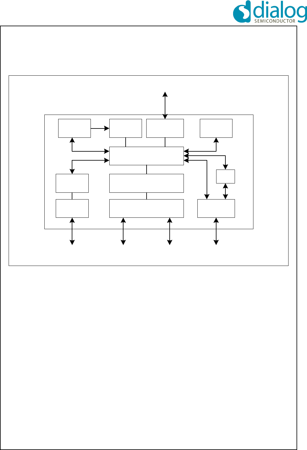
Figure 2 SC14CVMDECT SF functional overview
FLASH User SW UART XTAL
Phoenix Host API
CODEC / PCM
API commands
UART interface to host
SPI
Ports
Port PinsPCM PortHead SetDECT RF
DSP
Protocol
Stack
Radio
SC14CVMDECT SF Cordless Voice Module
© 2012 Dialog Semiconductor B.V. 11 July 1, 2014 v1.6
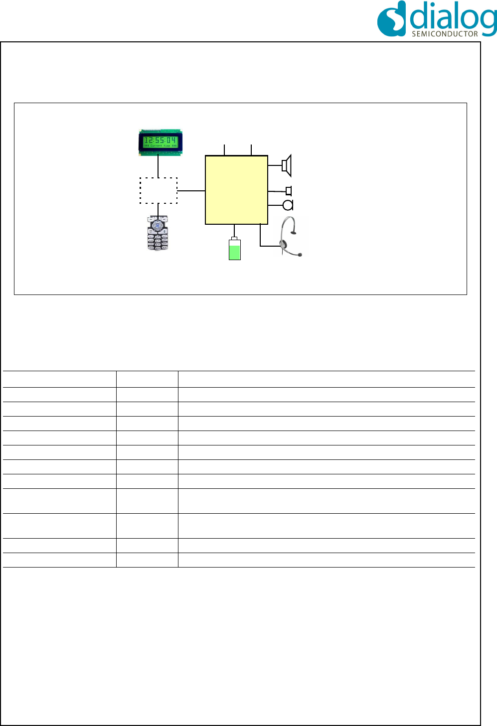
3.4 PORTABLE PART CONFIGURATION
A Portable Part configuration with SC14CVMDECT SF
requires additional external parts as shown in Figure 3. .
Table 2 provides an overview of the supported inter-
faces for a portable part.
Note 4: AFE setting is configurable, refer to document [2].
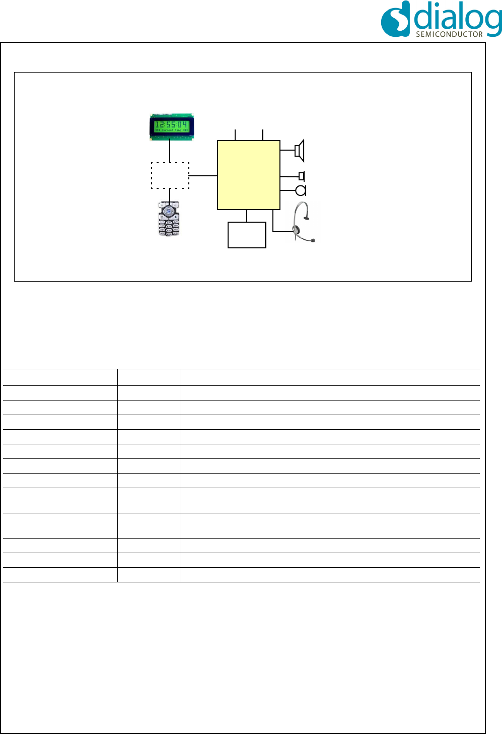
3.5 FIXED PART CONFIGURATION
A Fixed Part configuration with SC14CVMDECT SF
requires additional external parts as shown in Figure 4.
Figure 3 PP configuration
SC14CVMDECT
Loudspeaker
MIC (handset)
Earpiece (handset)
MCU
Headset
UART
Ports PCM
Table 2: PP support overview
Item Supported Remark
Battery management Yes Supported by API
Keypad No On external MCU
Display No On external MCU
IO Ports Yes All digital IO port pins can be controlled by API
PCM interface Yes 1x 16 bits serial I/O, PCM_FSC 8 kHz/16 kHz
UART Yes 115.2 kbit/s, used for API-commands
Headset detection Yes Supported by API
LSR (Earpiece, headset) Yes Connected to LSRp and/or LSRn
supports single-end and differential (Note 4)
MIC (Earpiece, headset,
handsfree)
Yes Connected to MICp and/or MICn and/or MICh
supports single-ended and differential (Note 4)
Handsfree speaker Yes Connected to PAOUTp/n (Note 4)
Radio Yes Integrated single antenna and support for external antenna(s)
SC14CVMDECT SF Cordless Voice Module
© 2012 Dialog Semiconductor B.V. 12 July 1, 2014 v1.6
.
Table 3 provides the overview of required and availa-
ble interfaces for a basic or a feature rich cordless FP
with the SC14CVMDECT SF. .
Note 5: AFE setting is configurable, refer to document [1].
3.6 VOICE COMMUNICATION
An FP supports up to 6 registered PPs, where 4 of
these PPs can be in a call at the same time. Multiple
simultaneous calls are supported. Supported voice
codec is G.726 (32 kbit/s ADPCM) and G.722 (64 kbit/s
ADPCM). See Figure 5.
3.7 LIGHT DATA APPLICATION
The SC14CVMDECT SF supports Low Data Rate
(LDR) transmission up to 1.6 kbit/s with IWU to IWU
messaging. The LDR can be used in combination with
voice communication. See Figure 5.
3.8 LU10 DATA APPLICATION
The SC14CVMDECT SF supports CAT-iq LU10 data
transmission up to 54 kbit/s. Since LU10 data commu-
nication uses the B-Field it cannot be used in combina-
tion with voice communication. See Figure 6.
Figure 4 FP configuration
SC14CVMDECT
Loudspeaker
MIC (handset)
Earpiece (handset)
MCU
Supply
Ports
Headset
Regulator
PCM
UART
Table 3: FP support overview
Item Supported Remark
Supply Regulator No Use external 3.3 V LDO
Keypad No On external MCU
Display No On external MCU
IO Ports Yes All digital IO port pins can be controlled via API
PCM interface Yes 4x 16 bits serial I/O, PCM_FSC 8 kHz/16 kHz
UART Yes 115.2 kbit/s, used for API-commands
Headset detection No Not supported by API
LSR (Earpiece, headset) Yes Connected to LSRp and/or LSRn
supports single-end and differential (Note 5)
MIC (Earpiece, headset,
handsfree)
Yes Connected to MICp and/or MICn and/or MICh
supports single-end and differential (Note 5)
Handsfree speaker Yes Connected to PAOUTp/n (Note 5)
PSTN Line interface No Not supported by API
Radio Yes Integrated single antenna and support for external antenna(s)
SC14CVMDECT SF Cordless Voice Module
© 2012 Dialog Semiconductor B.V. 13 July 1, 2014 v1.6
Figure 5 Voice and LDR data communication
G.726 + 1.6 kbit/s
G.722 + 1.6 kbit/s
SC14CVMDECT
SC14CVMDECT
SC14CVMDECT
PP
FP
PP
Figure 6 LU10 data application
54 kbit/s
54 kbit/s
SC14CVMDECT
SC14CVMDECT
SC14CVMDECT
PP
FP
PP
SC14CVMDECT SF Cordless Voice Module
© 2012 Dialog Semiconductor B.V. 14 July 1, 2014 v1.6
3.9 GENERAL FEATURES
Standard FP audio control feature.
Note 6: These features can be supported by combined API commands in user software.
Table 4: Supported general features
Functionality (Note 6) PP
support
FP
support Remark
Call handling
Conferencing - Yes Call between FP and 4x PP
Intercom Yes Yes Call between FP and 4x PP
Walkie Talkie mode Yes - Call between PP and PP without FP
Baby monitor Yes - Voice Activated PP. See document reference [2]
Voice over PCM interface Yes Yes -law (64 kbit/s), A-law (64 kbit/s), G.726 ADPCM
(32 kbit/s), G.722 ADPCM (64 kbit/s), Linear (128 kbit/s)
Call transfer Yes Yes Transfer call between PPs on FP
Page call Yes Yes FP pages all PPs (PP locator)
Protocol
Manual registration Yes Yes
Number of registered PPs per FP Yes - 1 to 6
Audio and tone
Microphone mute Yes Yes
Tone generation Yes No Melody generator with 7 polyphonic tones
Audio Volume control Yes Yes
Tone Volume control Yes No
Headset support Yes Yes
Handsfree/Speakerphone Yes No
General
Real time clock Yes Yes Accuracy depending directly on crystal
Real time clock synchronization Yes Yes All PP clocks are kept in synchronization with the FP
SW EEPROM (VES) Storage Yes Yes Internal on module
Battery Charge Management Yes No
PSTN line interface support - No PSTN software on request
I/O port support Yes Yes
Port Interrupt support No No
Automatic headset detection Yes No
Low speed data Yes Yes 1.6 kbit/s
LU10 data channel Yes Yes 54 kbit/s
CAT-iq up to version 2.0, 3.0 Yes Yes
ULE applications - Yes Number of ULE subscriptions: up to 180.
SC14CVMDECT SF Cordless Voice Module
© 2012 Dialog Semiconductor B.V. 15 July 1, 2014 v1.6
4.0 Functional description
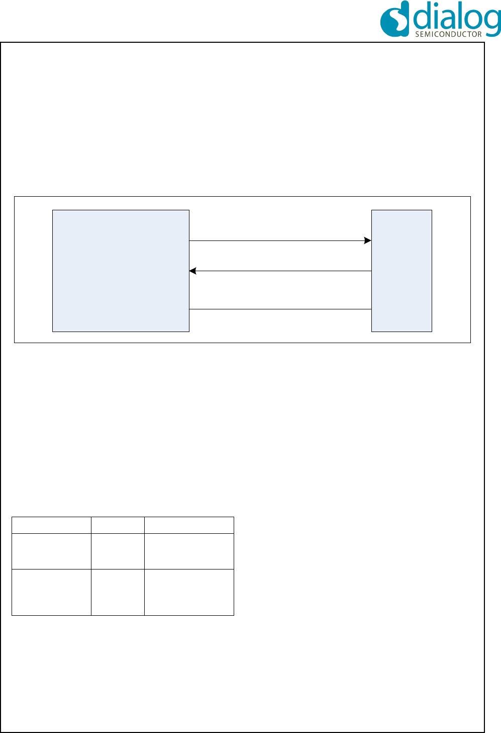
4.1 UART INTERFACE
The UART is normally used for API commands, but
can also be used for software upgrades and debug-
ging.
The UART is a full duplex UART with frame type:
1 start bit,
8 data bits (LSB first),
1 stop bit,
no parity,
up to 115.2 kBd.
The UART hardware interface uses only TX/RX
(see Figure 7).
Caution: All signals are 1.8 V (see Table 8, Table 9
and Table 10). An external V.24 line driver must be
provided if the UART port of the module is connected
to a standard V.24 device. Connecting the module
without a driver may damage the module.
4.2 VES (VIRTUAL EEPROM Storage)
4.2.1 VES layout
The SC14CVMDECT SF PP and FP include a 4 kB
VES which is divided into two areas (see Table 5).
VES is supported as virtual EEPROM with the internal
FLASH.
A detailed overview of the VES parameters can be
found in document reference [4].
Some parts of the VES parameters are read into the
SC14CVMDECT SF during the start up and other parts
are used by the SC14CVMDECT SF software during
execution.
The VES parameters are divided into 2 types:
• Factory type
• Normal type
The factory type is specific for the SC14CVMDECT SF
and should only be set by production. The factory type
parameters are either adjustments used by the base-
band or the radio interface, or are used to set up the
SC14CVMDECT SF into special modes. The factory
type parameters will only be modified by changing the
factory programmed default value. See document ref-
erence [4].
The “normal” VES parameters can be reset to their
default values via software.
4.2.2 VES access by MCU
The host is able to read or modify the VES parameters
or limited free VES areas via API command.
4.3 AUDIO CONFIGURATIONS
The SC14CVMDECT SF audio supports standard
DECT audio qualities. The audio gain and volume
parameters are placed in the VES. The DECT gains
can be adjusted to meet the TBR38 and TBR10 audio
level requirements by using the SC14CVMDECT SF
application reference design. For other line and acous-
tic designs it is required to adjust and tune the audio
setup.
Figure 7 UART hardware configuration
SC14CVMDECT MCU
TX (serial out), module pin 48
RX (serial in), module pin 47
GND
Table 5: VES map
VES space Size Usage
SC14CVMDECT
SF
3.6 kB Used for RF, audio,
battery, tone setup,
data base, etc.
User 0.4 kB Can be used for
MMI applications
such as User infor-
mation.
SC14CVMDECT SF Cordless Voice Module
© 2012 Dialog Semiconductor B.V. 16 July 1, 2014 v1.6
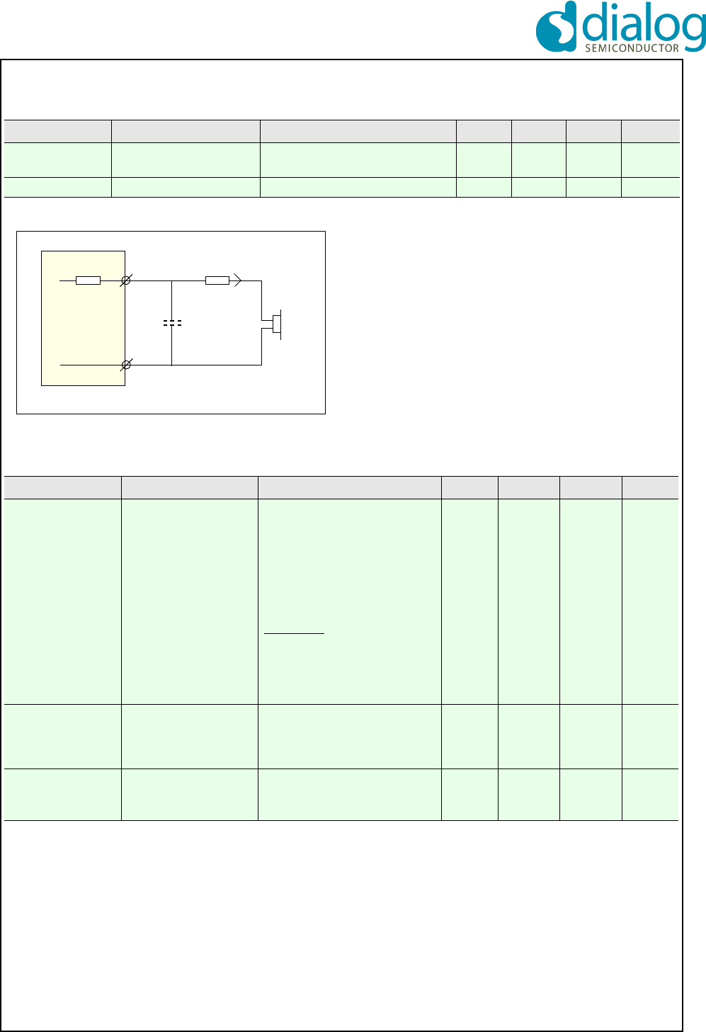
4.3.1 Audio connection
The SC14CVMDECT SF PP audio connections are
shown in Figure 8. Refer to "Example Application Dia-
gram" on page 43 for detailed component values.
.
Earpiece or small loudspeaker connection
The earpiece loudspeaker can be connected either dif-
ferentially or single-ended. Dynamic loudspeakers with
an impedance of 30 can be connected, as well as
ceramic loudspeakers equivalent to 600 and 30 F.
Refer to Table 16 for a detailed specification or the ear-
piece loudspeakers.
The earpiece is connected to the LSRp and LSRn pins.
Microphone connection
The microphone can be connected either single-ended
via MICp or differentially to MICp and MICn.
Headset connection
The headset microphone must be connected to the
MICh pin. The headset earpiece is connected to the
LSRp.
Microphone supply connection
For active microphones a voltage source with high sup-
ply voltage rejection ratio is provided on supply pins
VREFp/VREFm. Filtering of internal and external refer-
ence voltages is provided by an internal capacitor. No
external capacitor shall be connected to pin VREFp. To
avoid audible switching noise it is important that the
ground supply signals are directly “star point” con-
nected to the VREFm and not via a common ground
plane. From this VREFm star point, one connection is
made to the common ground plane.
Loudspeaker connection
For the handsfree operation a 4 loudspeaker must
be connected to the PAOUTp and PAOUTn pins as
shown in Figure 9. The VDDPA is the supply pin.
Refer to Table 19 for a detailed specification of the
external components around the loudspeaker. These
components are necessary to guarantee the lifetime of
the module.
Figure 8 Audio connections
LSRn
LSRp
MICh
MICn
VREFm
MICp
VREFp
Figure 9 Loudspeaker connection
PAOUTp
PAOUTn
VDDPA
VSS/GND
C_VDDPA
Cs_PAOUT
Rs_PAOUT
Cs_PAOUT
Rs_PAOUT
SC14CVMDECT SF Cordless Voice Module
© 2012 Dialog Semiconductor B.V. 17 July 1, 2014 v1.6
4.4 AUDIO ROUTING
4.4.1 FP AUDIO ROUTING
Figure 10 shows the audio routing for a FP. Input and
output signals are supported both for the internal codec
and the PCM, and the Air interface supports G.726
(32 kbit/s ADPCM) and G.722 (64 kbit/s ADPCM). The
internal software supports up to 4 audio channels
simultaneously. Supported sample rates are 8 kHz and
16 kHz.
FP does not support acoustic or line echo cancellation.
4.4.2 FP audio level adjustment
The internal codec audio levels can be controlled with
the parameters MicGain and LsrGain.
The MicGain range is 0 to 30 dB in steps of 2 dB and a
value of -128 will mute the input signal, default is 0 dB.
The LsrGain range is +2 dB to -12 dB in steps of 2 dB,
default is +2 dB. See document reference[1].
4.4.3 PP audio routing
Figure 11 and Figure 12 show the different audio rout-
ing modes of a PP. Figure 11 shows an overall audio
routing and Figure 12 shows the detailed audio routing
for the speakerphone of PP (FP does not support
speakerphone).
4.4.4 PP audio codec adjustment
The audio codec settings for the loudspeaker and
microphone must be pre-configured in the VES for
each mode. The VES parameter fields for
Audio.Earp.xxx
Audio.Heads.xxx
Audio.SpkPh.xxx
have a default value and maybe fine-tuned for the
application. See document reference[4].
4.4.5 General audio adjustment
For each audio mode, the receive (RLR) and transmit
(SLR) audio paths must be adjusted. RLR and SLR are
adjusted in the registers in the VES for each audio
state; see document reference [4]. Figure 13 shows
this image.
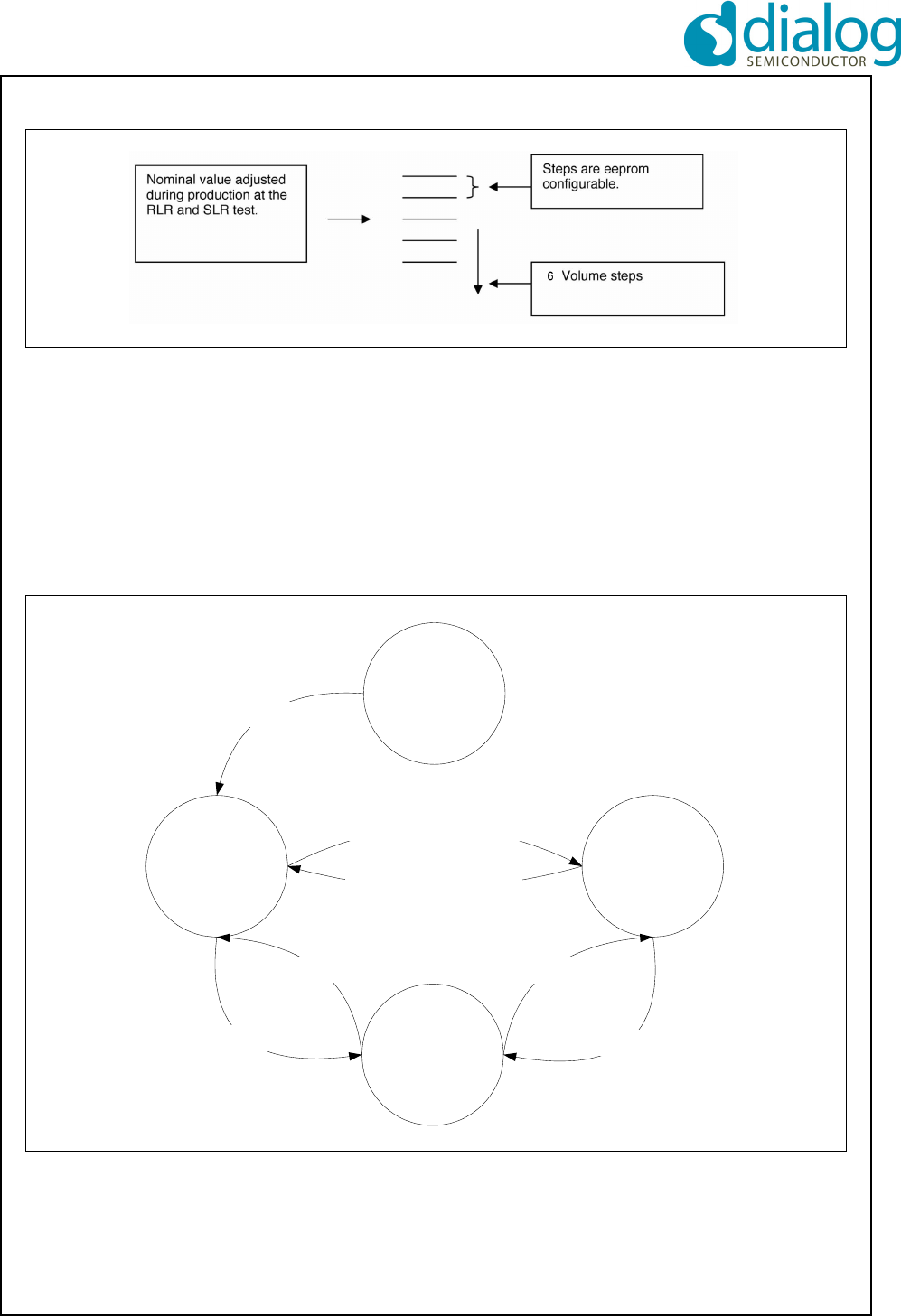
4.4.6 PP volume
The PP supports 6 volume steps, which are VES con-
figurable through parameter fields Audio.Earp.Vol.xxx,
the Audio.Heads.Vol.xxx and Audio.SpkPh.Vol.xxx.
The volume steps must be set initially in the VES dur-
ing production; see document reference [4].
4.4.7 PP audio equalization
To enable adjustments of the frequency response the
PP contains four programmable filters: 2 in RX direc-
tion and 2 in TX direction (see Figure 11).
By default these filters are loaded with bypass coeffi-
cients. These can be modified by loading new coeffi-
cients via API commands.
Equalizer filters are part of the audio routes for all
audio modes and are placed as shown in Figure 11.
For a detailed description of the filter functionality refer
to the API documentation; see document reference [2].
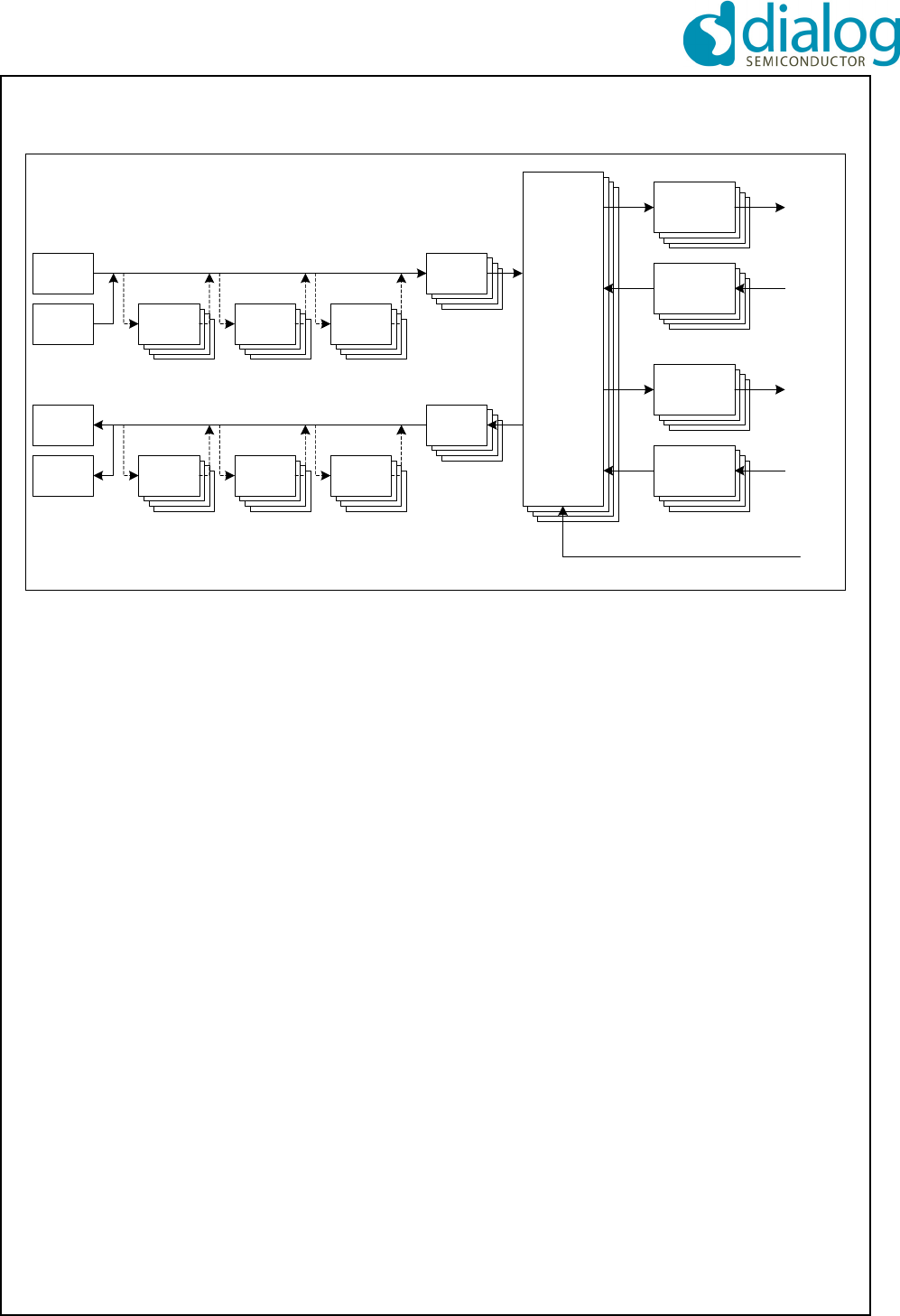
Figure 10 FP audio routing
Mask &
Shift
G726
Encoder
G726
Encoder
G726
Encoder
G726
Encoder
Mac
Rx
G726
Encoder
G726
Encoder
G726
Encoder
G726
Decoder
Mac
Tx
G726
Encoder
G726
Encoder
G726
Encoder
G722
Encoder
Mac
Rx
G726
Encoder
G726
Encoder
G726
Encoder
G722
Decoder
Mac
Tx
Mac
Unit
Soft Mute
(bit errors on air interface)
IoCtrl
IoCtrl
IoCtrl
IoCtrl
PCMx
In
Codec
In
PCMx
Out
Codec
Out
Mask &
Shift
Mask &
Shift
Mask &
Shift G711
Decoder
G711
Decoder
G711
Decoder
G711
Decoder
CWB
Unpack
CWB
Unpack
CWB
Unpack
CWB
Unpack
IoCtrl
IoCtrl
IoCtrl
IoCtrl
Mask &
Shift
Mask &
Shift
Mask &
Shift
Mask &
Shift G711
Decoder
G711
Decoder
G711
Decoder
G711
Encoder
CWB
Unpack
CWB
Unpack
CWB
Unpack
CWB
Pack
SC14CVMDECT SF Cordless Voice Module
© 2012 Dialog Semiconductor B.V. 18 July 1, 2014 v1.6
.
Figure 11 PP audio routing
Earpiece/Headset Mode
Idle Mode
ToneGen
SumUnit
TonegenAu_0
summ1
Mix_Ain_Tone
ECUnit
MicLevel
AnAgc
Analog AGC
ToneGen
SumUnit
TonegenAu_0
summ1
Mix_Ain_ToneEcho Canceller
EC1
type 2
A2_OUT
B2_IN
B1_OUT A1_IN
VolSideToneUnit
Handsfree Mode
Speaker
VOLCTRL
digitaloutgain
Limiter
RMSdetector
summ2
VolSideTone
EqUnit_0
VolSideToneUnit
Earpiece Earpiece
Rx Filters
PFILT 1-3 or
IIRSOS 1-3
Rx Filters
PFILT 1-3 or
IIRSOS 1-3
NC100Hz
RFI CancellerTx Filters
PFILT 1-3 or
IIRSOS 1-3
Pass Through
CodecUnit
EqUnit_0
EqUnit_1 RfiSuppUnit
Digital
Gain &
Limiter
Plvl
summ2
VolSideTone
ECUnit
MicLevel
AnAgc
Analog AGC
ToneGen
SumUnit
TonegenAu_0
summ1
Mix_Ain_ToneEcho Canceller
AEC/PAEC/
Handsfree
A2_OUT
B2_IN
B1_OUT A1_IN
VolSideToneUnit
Rx Filters
PFILT 1-3 or
IIRSOS 1-3
NC100Hz
RFI CancellerTx Filters
PFILT 1-3 or
IIRSOS 1-3
Pass Through
CodecUnit
EqUnit_0
EqUnit_1 RfiSuppUnit
Digital
Gain &
Limiter
Plvl
summ2
VolSideTone
Noise
Gate
Noise Gate
NoiseGateUnit
Noise Gate only used together with PAEC
CNG
Comfort Noise
Generator
CngUnit Comfort Noise Generator only used together with PAEC
Figure 12 Extended speakerphone for PP
Filters
3 x biquad
Microphone Speaker
ClassD
Digital
Gain
VolSideTone
Peak
limiter
PAEC UNIT
Hfree
switch
x
x
RMS RMS
RMSRMS
PAEC
FFT
FFT
iFFT
PAEC engine
LMS
+
FIR
EC
gains
Filters
3 x biquad
Post gain
2x
Biquad
Air Interface
Rx Noise
Gate
Pre gain
Comfort
Noise
PAEC Rx Gain
SC14CVMDECT SF Cordless Voice Module
© 2012 Dialog Semiconductor B.V. 19 July 1, 2014 v1.6
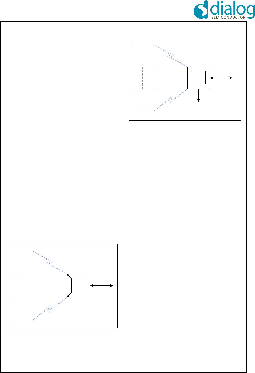
4.5 PP AUDIO MODES
The PP audio handling consists of four audio states
(see Figure 14). In these states the audio subsystem is
configured for a certain audio mode:
1. Idle mode (not relevant for microphone configu-
ration)
2. Earpiece mode (Handset speaker)
3. Handsfree or Speakerphone mode
4. Headset mode
Selection between the modes is done via API calls; see
document reference [2].
The Alert state is for tone playing and is entered auto-
matically when tones are played using the API calls.
The Alert state can originate from idle, earpiece,
handsfree or headset mode.
4.5.1 Power management
To minimize the current consumption the PP will shut
down all codec amplifiers in Idle mode. This means
that all reference voltages in the analog front-end will
be disabled. This feature can be disabled in the VES if
the reference voltages for some reasons are needed in
Idle mode.
Figure 13 Handset volume configuration
Figure 14 PP audio modes
Idle
Earpiece
Audio
Handsfree
Audio
API_PP_ AUDIO_SET_ MODE_ REQ
(API_ AUDIO_ MODE_ EARPIECE )
API_PP_ AUDIO_SET_ MODE_ REQ
(API_ AUDIO_ MODE_ EARPIECE )
API_PP_ AUDIO_SET_ MODE_ REQ
(API_ AUDIO_ MODE_ HANDSFREE )
Headset Audio
API_PP_ AUDIO_SET_ MODE_ REQ
(API_ AUDIO_ MODE_ HEADSET )
API_PP_ AUDIO_ SET_ MODE_ REQ
(API_ AUDIO_ MODE_ EARPIECE )
API_PP_ AUDIO_SET_ MODE_REQ
(API_ AUDIO_ MODE_ HEADSET)
API_PP_ AUDIO_ SET_ MODE_ REQ
( API_ AUDIO_ MODE_ EARPIECE )
SC14CVMDECT SF Cordless Voice Module
© 2012 Dialog Semiconductor B.V. 20 July 1, 2014 v1.6
4.5.2 Earpiece mode
In Earpiece mode (Handset speaker) an artificial
sidetone is generated. The level of the sidetone can be
adjusted and setup in the VES through parameter
fields Audio.Earp.Vol.Elementx, SideToneGain and
Audio.Heads. Elementx.SideToneGain. In Earpiece
mode it is possible to adjust the volume in the Earpiece
via API calls. In Earpiece mode the PP audio is routed
as shown in Figure 11.
4.5.3 Alert mode
The Alert mode is for generating tones and melodies
on the Speakerphone loudspeaker. In Alert mode it is
possible to adjust the volume in the speaker via API
calls. Inband tones will be affected by the volume
adjustments, since the volume control takes place after
tones are added to the signal. Figure 11 shows the
Audio flow.
4.6 CALL HANDLING
4.6.1 FP to PP call
When the FP initializes a call to a PP, a radio connec-
tion is set up to all PP applications to make it possible
for the PP application software to indicate that there is
an incoming call.
It is possible to configure the ringing indication using
broadcast to make all 6 PPs ringing.
4.6.2 PP to FP call
When the MMI software signals the PP to establish a
call, the PP opens the radio connection to the FP.
4.6.3 Intercom
Figure 15 shows the audio routing of an internal call
between PP1 and PP2. In the FP no transcoding takes
place.
4.6.4 Conference
Figure 16 shows the audio routing of a 9-party confer-
ence call.
4.6.5 Page call
The Page call is a FP functionality used to locate the
registered PPs. FP paging does not establish a normal
audio connection and is terminated when answered by
the PP.
4.7 TONE/MELODY HANDLING
The tone component handles the generation of various
tones in the device. Both tones/melodies in a PP con-
figuration are supported.
The main features of the tone component are:
• Ringer tones and melodies (7-tone polyphonic)
• Alert tones (key sound, error tones, confirmation
tones, etc.)
• Inband tones (dial tone, net-congestion tone, busy
tone, etc.)
• Single tone generation
4.8 DATE AND REAL-TIME CLOCK
The FP has a real-time clock feature, which (when acti-
vated) broadcasts the date and time of day to the PPs.
Activation of the date and real-time clock is done by
setting the date and time via the PP.
The clock supports hours, minutes and date. The date
supports leap years. Daylight saving time is not sup-
ported and must be handled by the MMI application.
The PP clock is synchronized with the FP every time a
broadcast is received. If the PP goes out-of-lock, the
PP itself calculates the clock time until the PP is again
within the range of the FP. The updated clock time can
be read locally via the MMI software.
To adjust the clock in the FP, a service connection can
be set up via commands from the PP.
The clock can also be read and set directly from an
external microprocessor or through the MMI software
on the FP.
The real-time clock accuracy depends directly on the
Figure 15 Intercom connection
CVMDECT
FP
CVMDECT
PP2
CVMDECT
PP1
PCM
Figure 16 Conference connection
CVMDECT
PP4
CVMDECT
PP1
4CH PCM
MIX
CVMDECT FP
Analog
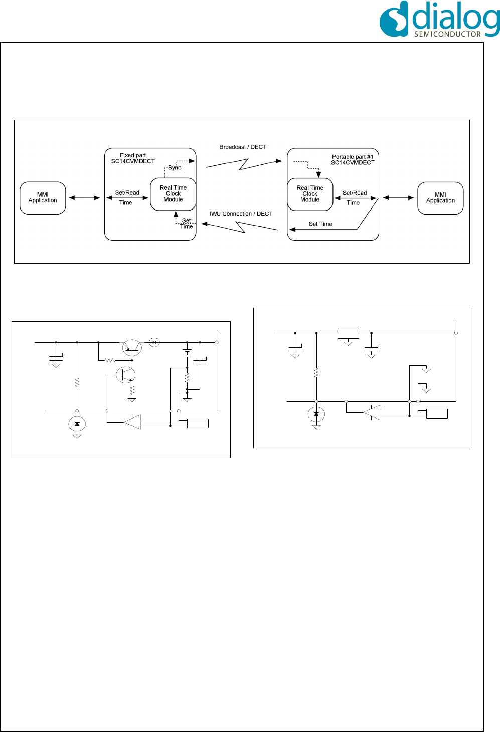
SC14CVMDECT SF Cordless Voice Module
© 2012 Dialog Semiconductor B.V. 21 July 1, 2014 v1.6
SC14CVMDECT SF crystal.
When the SC14CVMDECT SF is configured as a PP,
the clock has the same accuracy as the FP clock.
When the PP synchronises with a FP, the PP crystal is
synchronized with the FP crystal and the PP clock will
change accordingly.
The accuracy is expected to be within 1 minute for up
to 6 weeks without being locked to a FP.
4.9 BATTERY MANAGEMENT
Figure 18 shows a handset application with NiMH.
SOC (State Of Charge) is used to measure the amount
of charge in the rechargeable batteries.
Figure 19 shows an FP application. The FP uses an
external LDO, so the SOC pins are not used and can
be connected to GND.
The PP API supports battery management to calculate
the battery capacity and to indicate charge status.
Refer to API document [2].
The SOC circuit is used to very accurately determine
the amount of charge in rechargeable batteries as well
as the discharge state of Alkaline batteries. This infor-
mation is essential for the battery charging algorithm
and necessary for battery status indication to the user.
Battery status information is supported by the API.
Detailed information can be found in AN-D-174 (Bat-
tery Management).
Pin CHARGE_CTRL is driven high when either the
“sensed voltage on the VBAT pin” is lower than the
voltage setting or “sensed current via SOCp” is lower
than the current setting. Pin CHARGE_CTRL can drive
up to 500 A as source current (see Table 20).
Detailed setting information can be found in document
[4] under “Battery settings”.
4.10 PROTOCOL STACK
The protocol stack handles the RF interface, the MAC-,
DLC-, NWK-layer and encryption according to the
DECT standard EN300 175 1-9.
4.10.1 DECT TBR22
The SC14CVMDECT SF supports the DECT GAP
standard according to EN300 444. For TBR22 type
approval (optional) switching off the authentication and
encryption is required, which can be done with the VES
parameter Tbr_22.
Figure 17 Clock synchronization
Figure 18 Handset (PP) application with 2x NiMH
100
CHARGE_CTRL
1k
1k
0.1
SOC
CHARGE
SOCp
SOCn
Vsupply VBAT IN
Figure 19 Base station (FP) application
CHARGE_CTRL
1k
SOC
CHARGE
SOCp
SOCn
Vsupply VBAT IN
LDO

SC14CVMDECT SF Cordless Voice Module
© 2012 Dialog Semiconductor B.V. 22 July 1, 2014 v1.6
4.10.2 Out-of-Range handling
When the PP goes in-range or out-of-range a signal is
sent from the PP to the MMI software indicating
whether the PP is in-lock or is out-of-lock with the FP.
4.10.3 Preamble antenna diversity
To optimise the audio quality caused by rapidly chang-
ing radio paths (fading), the SC14CVMDECT SF sup-
ports preamble antenna diversity. The preamble
diversity algorithm uses RSSI measurements to judge
the radio signal strength on both antennas and, as a
result, the choice of the best performing antenna is
determined. This antenna will then be used for the
receive slot and the next transmit slot.
The preamble antenna diversity is supported with two
antennas. The preamble diversity can be controlled by
VES. See document reference [4] and Section 4.13 for
more information about antenna diversity.
4.10.4 Broadcasting messages
Messages consisting of up to 19 bytes can be broad-
casted from FP to all registered PPs. Broadcasting
does not require an active connection. Broadcasting
does not use retransmission, therefore broadcasting is
not secured. If the real time clock is enabled this data is
also broadcasted to all PPs.
4.10.5 IWU to IWU messaging
The protocol in the SC14CVMDECT SF module is
made according to the DECT/GAP standard as defined
in EN 300 175 and EN 300 444.
The DECT standard defines an EMC code (see
EN 300 175-5, chapter 7.7.23.). This code is unique for
a DECT product and must be programmed by the
DECT manufacturer to the correct manufacturer code.
The EMC code must be the same for SC14CVMDECT
SF based product families when using the IWU to IWU
messaging.
If the Dialog default EMC VES value is changed the
IWU to IWU messaging may not operate correctly.
IWU data is transferred in a FA format frame; see
chapter 6.1 in EN 300 175-4. This frame has an infor-
mation field of maximum 63 bytes of which maximum
52 bytes can be used for IWU data. With the
SC14CVMDECT SF it is only possible to send
5 frames in a row without pause. The following frame
must be an acknowledge-frame to secure that the
internal buffers within the SC14CVMDECT SF are
emptied.
The FA frame is segmented in 5 byte fragments and
transferred over the air-interface in the A-field. The 2-
bytes CRC is used to determine if the data is received
correctly. If the data is not received correctly this is sig-
nalled back to the transmitter by the Q2 bit, and the
data is retransmitted.
The FA frame has a 2 bytes checksum, used to deter-
mine if the complete packet is received correctly. If A
checksum error is signalled back to the transmitter and
the complete packet is retransmitted. The packet will
be retransmitted until it is received correctly, or until the
link is closed.
More transmitted packets will be received in the same
order as they were transmitted. The application must
handle flow control, if needed.
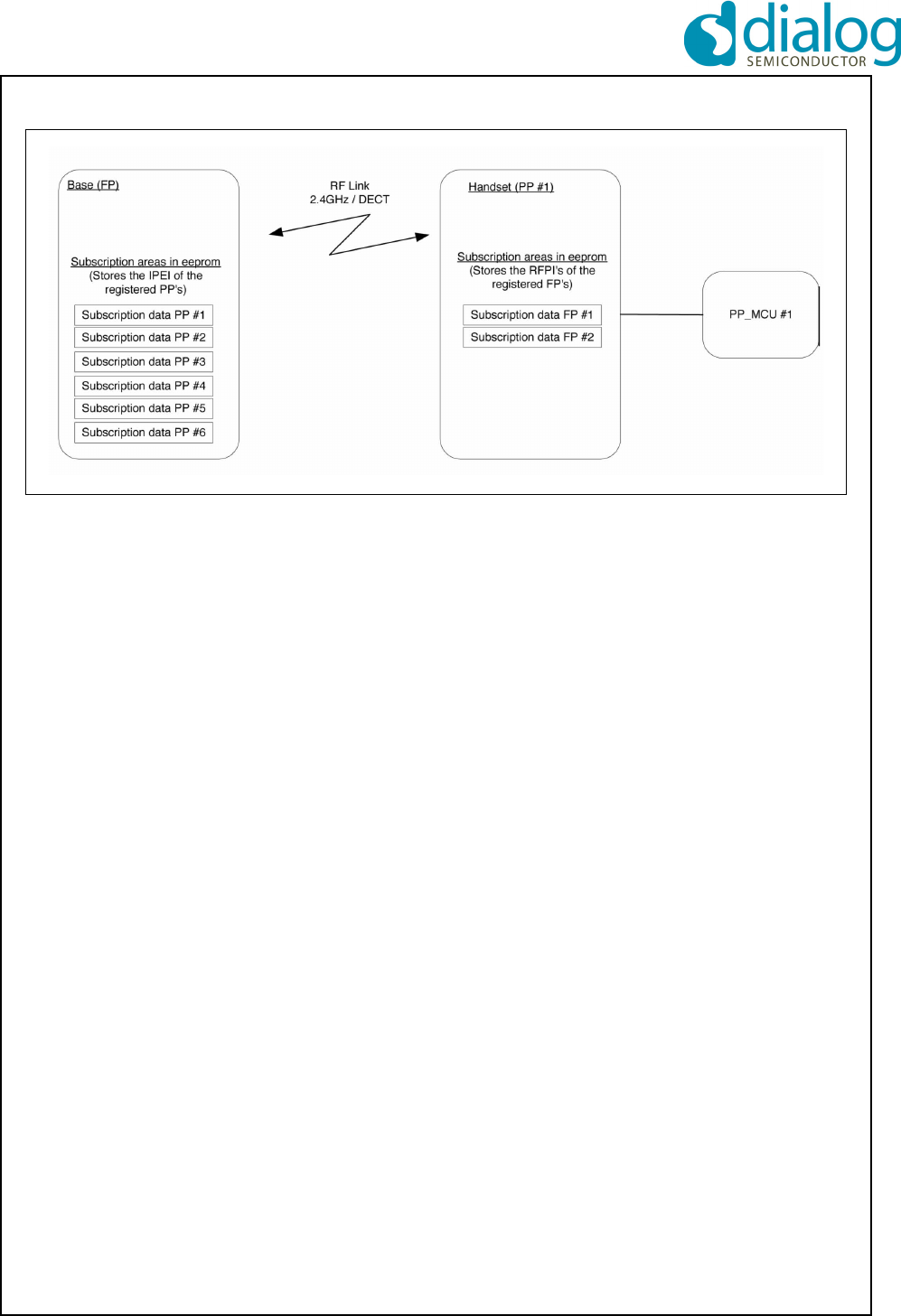
4.11 REGISTRATION
The PP and the FP must be paired using a procedure
called Registration. Without Registration, the PP will be
out-of-lock and will not be able to establish a link to a
FP and therefore not be able to make a call. The regis-
tration uses the unique product identities and secures
the PP and FP to allow no cross-communication.
The PP can be de-registered from a FP either via the
FP or PP MMI Software using the command interface.
It is also possible to deregister a PP from another reg-
istered PP.
It is possible to pair a PP and FP during the production.
4.11.1 Handling product identities
To secure that the FP and PPs do not make cross-
communications a unique ID must be entered into the
VES of an FP or PP. For the DECT version the ID for
the FP is named RFPI and for the PP the ID is named
IPEI. These numbers are factory settings.
After a successful registration, the IPEI is stored in the
FP and the RFPI is stored in the PP. In this way the two
parts are known to each other and are allowed to make
connections. The registration data are automatically
stored in VES of the FP and PP while making the regis-
tration.
It is possible to register the same PP to 2 FPs, but it
can only be used in one FP at the same time.
SC14CVMDECT SF Cordless Voice Module
© 2012 Dialog Semiconductor B.V. 23 July 1, 2014 v1.6
4.11.2 Deregistration
There are two ways of deregistering a PP from an FP:
• Remote FP and PP deregistration
The correct way to deregister a PP from an FP is to
deregister it remotely in the FP. If this is done over a
service connection from the PP to the FP, the FP
actually performs the deregistration and then it is
automatically signalled to the PP which in turn will
drop out-of-lock. Using this method it is also possible
to deregister other PPs registered to the FP from
one PP.
• Removing all registrations at once from the FP (e.g.
in case the original PPs are lost).
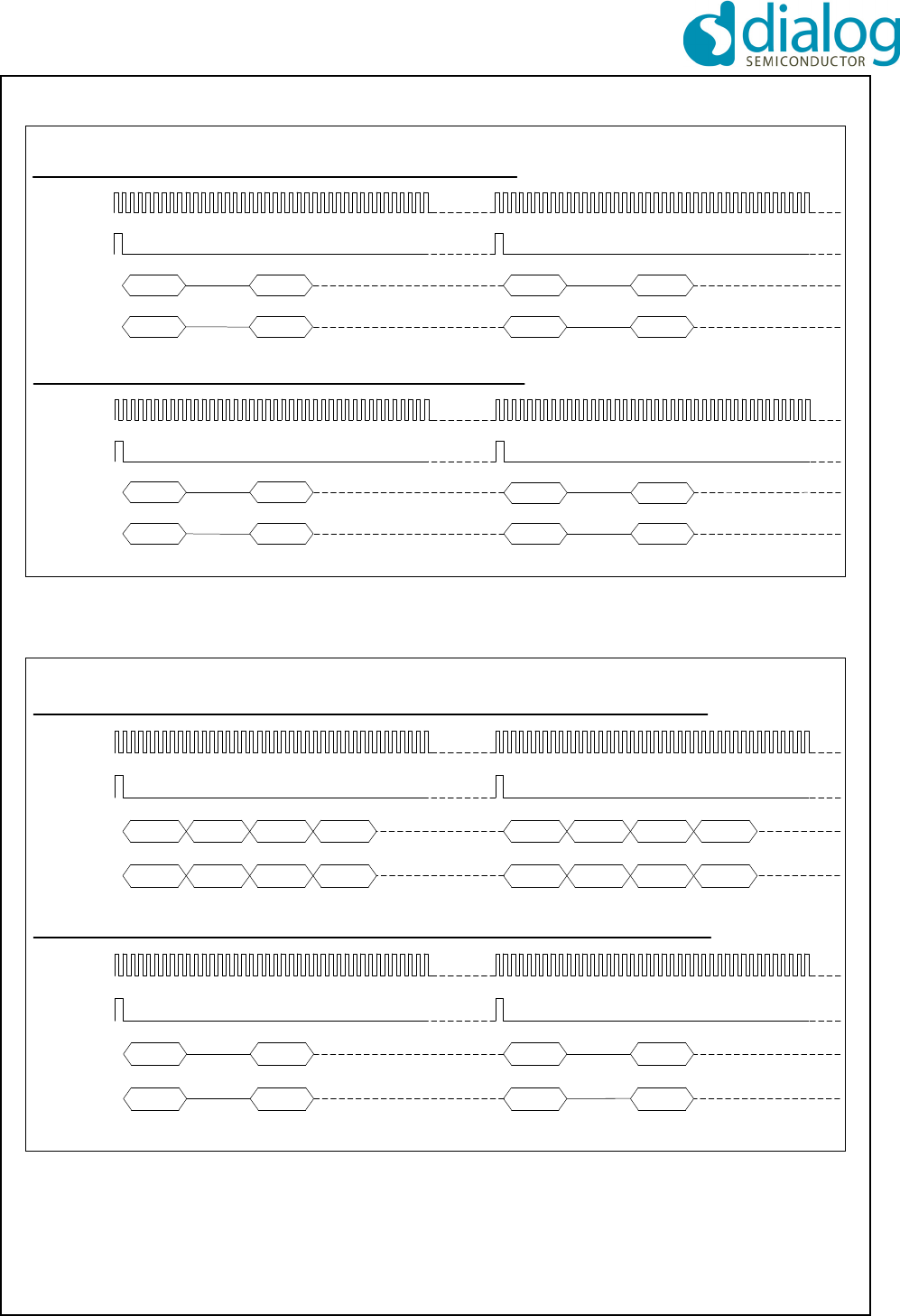
4.12 PCM INTERFACE
The PCM supports the following modes:
• SLAVE mode clock sync. In this mode the clock of
the module will be adjusted to follow the PCM pro-
vided by the external PCM master clock. All audio
samples are kept if the provided PCM clock accu-
racy is +/- 5 ppm, which is a DECT radio require-
ment.
• SLAVE no clock sync. In this mode the clock of the
module is not synchronized. This means audio sam-
ple will be discarded in case the master PCM clock
is faster than the clock of the module or samples will
be repeated in case the master PCM clock is slower.
• MASTER mode. The FP is master on PCM interface
and therefore provides PCM clock and PCM_FSC to
an external device.
4.12.1 PCM Interface for FP
The SC14CVMDECT SF supports PCM interface func-
tionality to connect to an external audio source/destina-
tion.
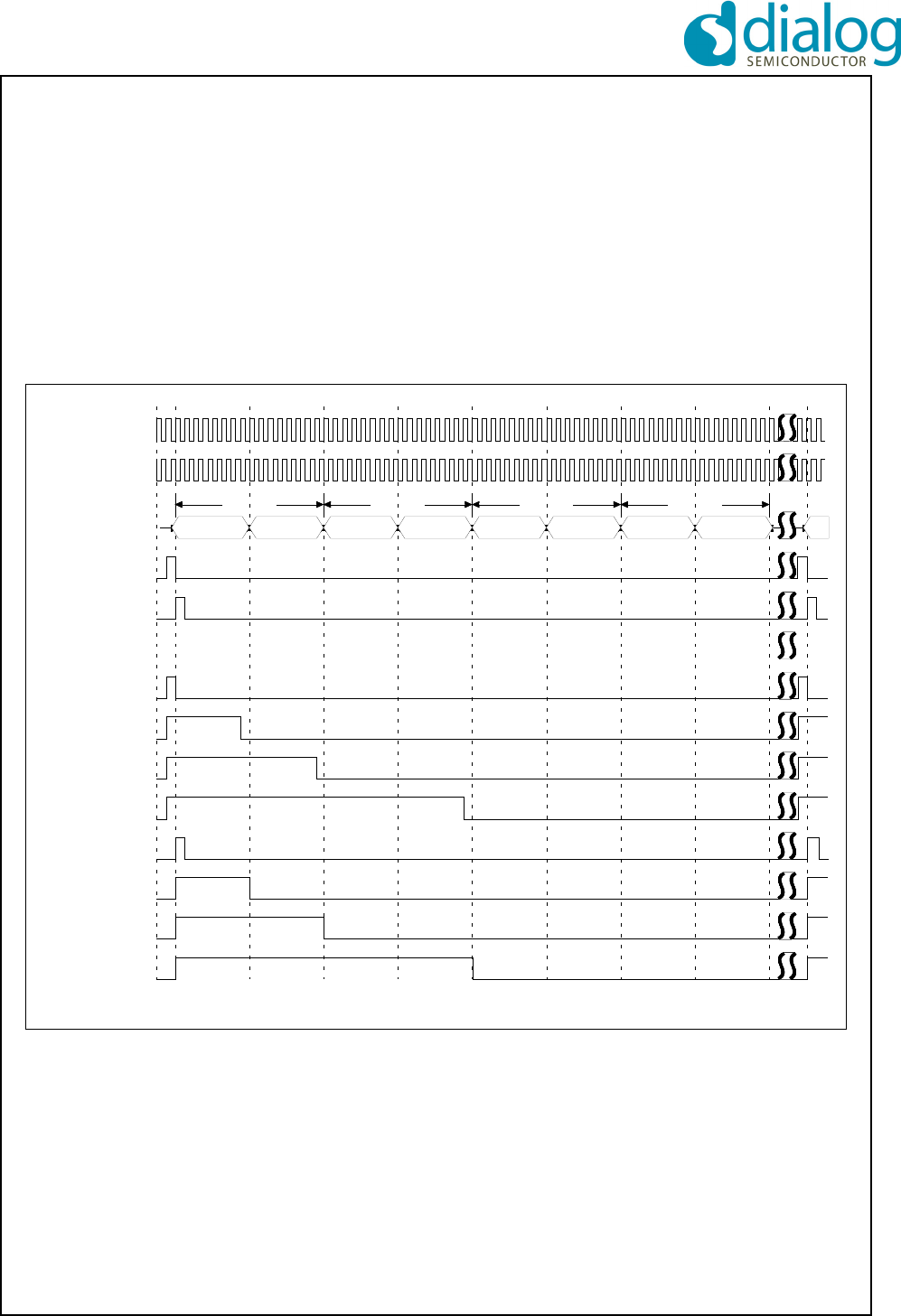
The different PCM interface modes and timings are
shown in Figure 21 to 26. Refer to document [1] for
detailed information.
4.12.2 PCM_FSC frequency
The PCM interface supports the following options:
• 8 kHz
• 16 kHz
4.12.3 Length of PCM_FSC
The PCM interface supports the following options:
• 1: The length of PCM_FSC pulse is equal to
1 data bit.
• 8: The length of PCM_FSC pulse is equal to
8 data bits.
• 16: The length of PCM_FSC pulse is equal to
16 data bits.
• 32: The length of PCM_FSC pulse is equal to
32 data bits.
4.12.4 Start position of FSC
The PCM interface supports the following options:
• The FSC pulse starts 1 data bit before
the MSB bit of the PCM channel 0 data.
• The FSC pulse starts at the same time as
the MSB bit of the PCM channel 0 data.
4.12.5 PCM clock frequency
The PCM interface supports the following options in
master mode:
• 1.152 MHz
• 2.304 MHz
Figure 20 Handling product identities
SC14CVMDECT SF Cordless Voice Module
© 2012 Dialog Semiconductor B.V. 24 July 1, 2014 v1.6
• 4.608 MHz
• 1.536 MHz
4.12.6 PCM data mode
The PCM interface supports the following PCM data
formats:
• Linear PCM, 8 kHz sample rate.
Used for narrowband calls (G.726).
• Linear PCM, 16 kHz sample rate.
Used for wideband calls (G.722).
• G.711 – A-law, 8 kHz sample rate.
Used for narrowband calls (G.726).
• G.711 – -law, 8 kHz sample rate.
Used for narrowband calls (G.726).
• Compressed wideband using A-law, 16 kHz sample
rate. The 16 bit PCM data is encoded as two 8 bit
audio samples if 8 kHz frame sync is used. Used for
wideband calls (G.722).
• Compressed wideband using -law, 16 kHz sample
rate. The 16 bit PCM data is encoded as two 8 bit
audio samples if 8 kHz frame sync is used. Used for
wideband calls (G.722).
Figure 21 PCM interface formats
Channel 3Channel 3Channel 2Channel 2Channel 1Channel 1Channel 0Channel 0
DSP_PCM_CTRL_REG[5,4,3] = 000
DSP_PCM_CTRL_REG[5,4,3] = 010
DSP_PCM_CTRL_REG[5,4,3] = 100
DSP_PCM_CTRL_REG[5,4,3] = 101
DSP_PCM_CTRL_REG[5,4,3] = 111
DSP_PCM_CTRL_REG[5]=0
DSP_PCM_CTRL_REG[5]=1
PCM Slave mode
D15 D8 D7 D0
PCM Master
DSP_PCM_CTRL_REG[5,4,3] = 001
DSP_PCM_CTRL_REG[5,4,3] = 011
DSP_PCM_CTRL_REG[5,4,3] = 110
PCM_CLK
PCM_CLK
PCM_DI PCM_DO
PCM_FSC (input)
PCM_FSC (input)
PCM_FSC
PCM_FSC
PCM_FSC
PCM_FSC
PCM_FSC
PCM_FSC
PCM_FSC
PCM_FSC
SC14CVMDECT SF Cordless Voice Module
© 2012 Dialog Semiconductor B.V. 25 July 1, 2014 v1.6
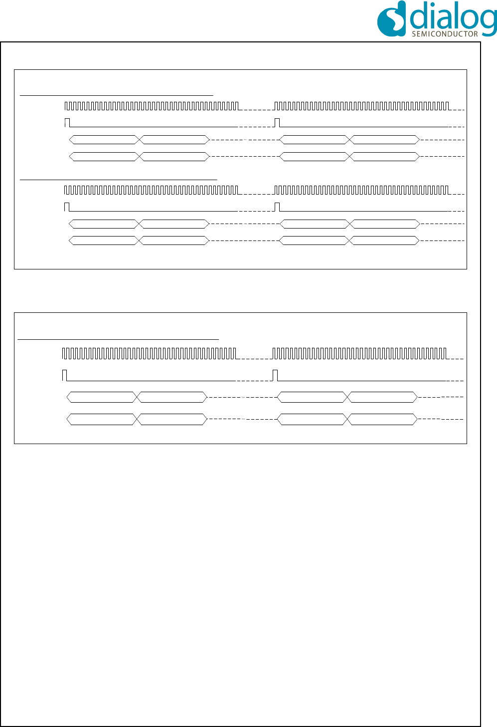
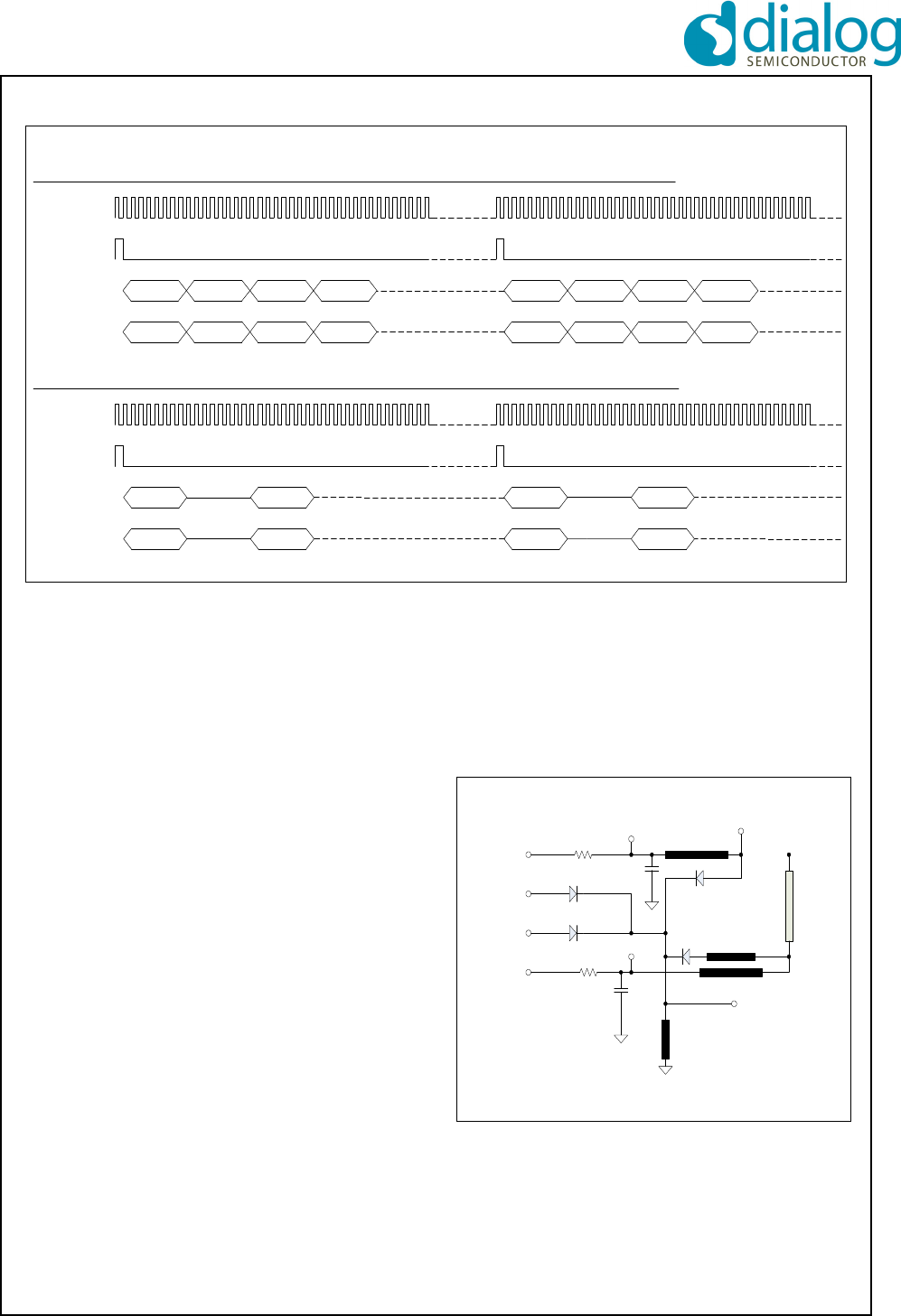
Figure 22 PCM bus with linear PCM, 8 kHz sample rate
PCM CLK
8 KHz FSC
PCM in
PCM out
Channel 0
Channel 0
Channel 1
Channel 1
Channel 0
Channel 0
Channel 1
Channel 1
AP_DATA_FORM AT_LINEAR_8kHz with 8 kHz frame sync:
1st fram e 2nd fram e1st
fram e
1st fram e 1st
fram e
2nd fram e
2nd fram e 2 nd fram e
PCM CLK
16 KHz FSC
PCM in
PCM out
Channel 0
Channel 0
Channel 1
Channel 1 Channel 0 Channel 1
1st fram e 1st fram e
1st fram e 1st fram e
AP_DATA_FORM AT_LINEAR_8kHz with 16 kHz frame sync:
1st fram e 1st fra m e
Channel 0 Channel 1
1st fram e 1st fram e
Figure 23 PCM bus with linear PCM, 16 kHz sample rate
PCM CLK
16 KHz FSC
PCM in
PCM out
Channel 0
Channel 0
Channel 1
Channel 1
Channel 0
Channel 0
Channel 1
Channel 1
1st frame 2nd frame1st frame
1st frame 1st frame
2nd frame
2nd frame 2nd frame
AP_DATA_FORMAT_LINEAR_16kHz with 16 kHz frame sync:
SC14CVMDECT SF Cordless Voice Module
© 2012 Dialog Semiconductor B.V. 26 July 1, 2014 v1.6
Figure 24 PCM bus with G.711 – A-law/-law, 8 kHz sample rate
PCM CLK
8 KHz FSC
PCM in
PCM out
Channel 0
Channel 0
Channel 1
Channel 1
Channel 0
Channel 0
Channel 1
Channel 1
AP_DATA_FORMAT_G711A / AP_DATA_FORMAT_G711U with 8 kHz frame sync:
1st frame
1st frame
2nd frame
2nd frame
1st frame
1st frame
2nd frame
2nd frame
PCM CLK
16 KHz FSC
PCM in
PCM out
Channel 0
Channel 0
Channel 1
Channel 1 Channel 0 Channel 1
AP_DATA_FORMAT_G711A / AP_DATA_FORMAT_G711U with 16 kHz frame sync:
1st frame
1st frame
1st frame
1st frame 1st frame 1st frame
Channel 0 Channel 1
1st frame 1st frame
Figure 25 PCM bus with compressed wideband using A-law/ -law, G722 used on air interface
PCM CLK
16 KHz FSC
PCM in
PCM out
Channel 0
Channel 0
Channel 1
Channel 1
Channel 0
Channel 0
Channel 1
Channel 1
AP_DATA_FORMAT_CWB_ALAW / AP_DATA_FORMAT_CWB_ULAW with 16 kHz frame sync (G.722 used on air):
1st frame
1st frame
1st frame
1st frame
2nd frame
2nd frame
2nd frame
2nd frame
PCM CLK
8 KHz FSC
PCM in
PCM out
Channel 0
Channel 0
Channel 1
Channel 1
Channel 0
Channel 0
Channel 1
Channel 1
Channel 0
Channel 0
Channel 1
Channel 1
Channel 0
Channel 0
Channel 1
Channel 1
AP_DATA_FORMAT_CWB_ALAW / AP_DATA_FORMAT_CWB_ULAW with 8 kHz frame sync (G.722 used on air):
1st frame
1st frame
2nd frame
2nd frame
1st frame
1st frame
2nd frame
2nd frame
3rd frame4th frame 3rd frame4th frame
4th frame 3rd frame4th frame3rd frame
SC14CVMDECT SF Cordless Voice Module
© 2012 Dialog Semiconductor B.V. 27 July 1, 2014 v1.6
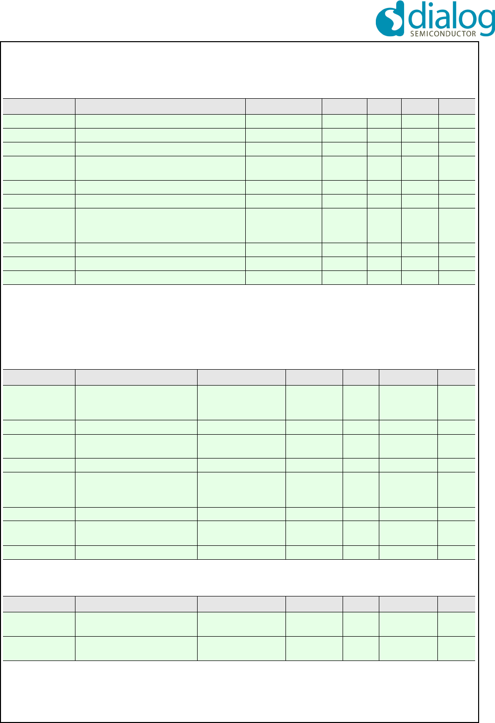
4.12.7 PCM Interface for PP
The SC14CVMDECT SF supports PCM interface func-
tionality to connect to an external audio source/destina-
tion. Refer to document [2] for detailed information.
• PCM interface mode
supports only master mode.
• PCM_FSC frequency
supports 8 kHz and 16 kHz.
• LENGTH of PCM_FSC
The PCM interface supports the following options:
• 1: The length of PCM_FSC pulse is equal to 1
data bit.
• 8: The length of PCM_FSC pulse is equal to 8
data bits.
• 16: The length of PCM_FSC pulse is equal to 16
data bits.
• 32: The length of PCM_FSC pulse is equal to 32
data bits.
• Start position of FSC
The PCM interface supports the following options:
• The FSC pulse starts 1 data bit before MSB bit of
the PCM channel 0 data.
• The FSC pulse starts at the same time as the
MSB bit of the PCM channel 0 data.
• PCM clock
PCM clock is delivered to an external slave PCM
device from SC14CVMDECT SF.
• PCM Data mode
Supports only linear 16 bit PCM.
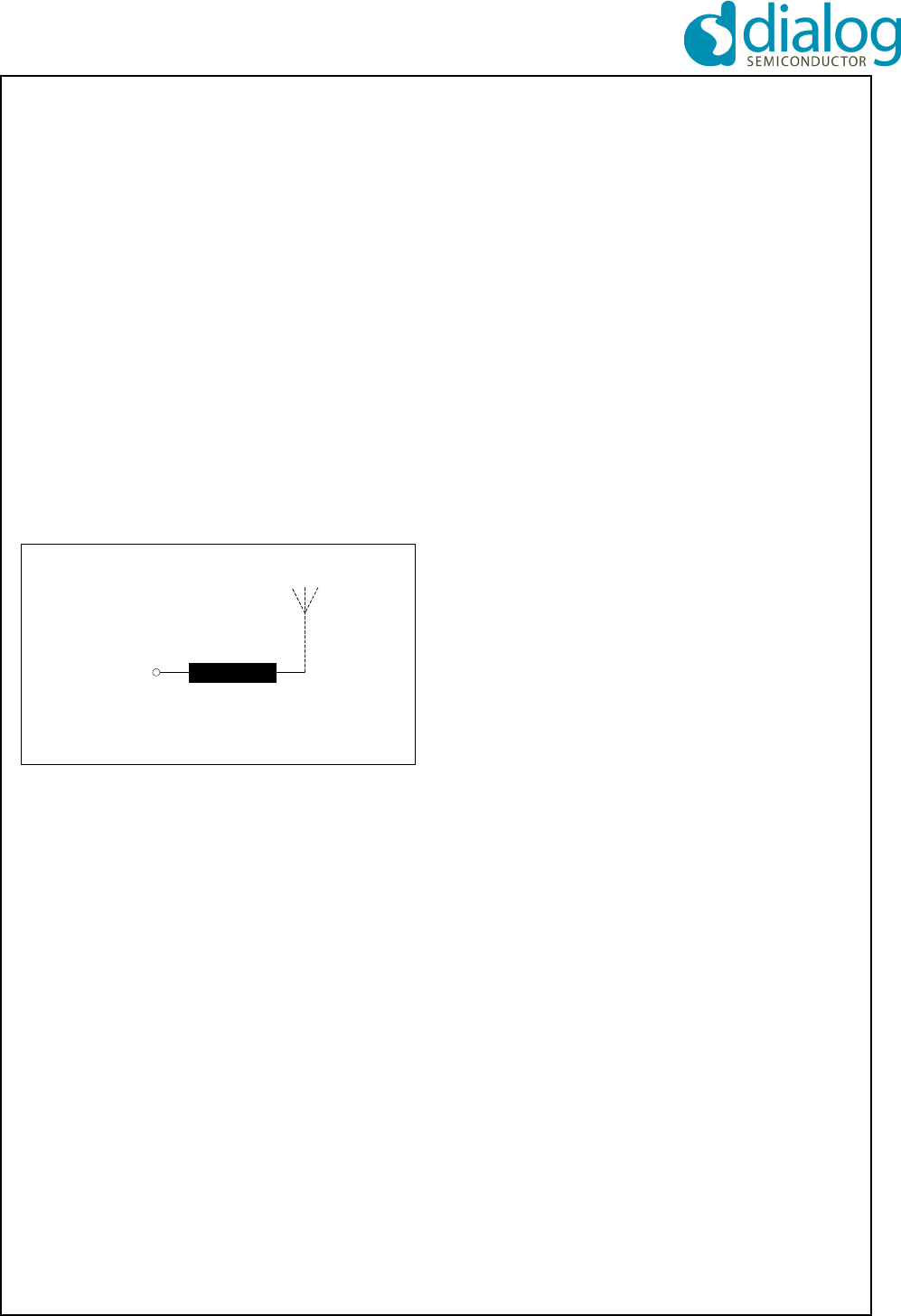
4.13 ANTENNA OPERATION
Figure 27 shows the internal circuit of the
SC14CVMDECT SF. Pin RF0 is used for two external
antennas and can also be used for RF test purposes,
so it is recommended to add a 10 pF capacitor as
reserve pattern even when the two external antennas
are not used.
Figure 26 PCM bus with compressed wideband using A-law/ -law, G726 used on air interface
PCM CLK
16 KHz FSC
PCM in
PCM out
Channel 0
Channel 0
Channel 1
Channel 1
Channel 0
Channel 0
Channel 1
Channel 1
AP_DATA_FORMAT_CWB_ALAW / AP_DATA_FORMAT_CWB_ULAW with 16 kHz frame sync (G.726 on air):
1st frame
1st frame
1st frame
1st frame
PCM CLK
8 KHz FSC
PCM in
PCM out
Channel 0
Channel 0
Channel 1
Channel 1
Channel 0
Channel 0
Channel 1
Channel 1
Channel 0
Channel 0
Channel 1
Channel 1
Channel 0
Channel 0
Channel 1
Channel 1
AP_DATA_FORMAT_CWB_ALAW / AP_DATA_FORMAT_CWB_ULAW with 8 kHz frame sync (G.726 on air):
1st frame
1st frame
2nd frame
2nd frame
1st frame
1st frame
2nd frame
2nd frame
2nd frame
2nd frame
2nd frame
2nd frame
1st frame
1st frame
1st frame
1st frame
1st frame
1st frame
1st frame
1st frame
Figure 27 Internal circuit of the SC14CVMDECT SF
RF1
TP1
Internal antenna
RF0
P0n
P0
TX
RX
RFP0n
RFP0
SC14CVMDECT SF Cordless Voice Module
© 2012 Dialog Semiconductor B.V. 28 July 1, 2014 v1.6
Re-certification of the SC14CVMDECT SF is required if
at least one external antenna is added. On request,
Dialog Semiconductor can provide a pre-certified PCB
layout for an external antenna circuit.
RF1 is also recommended to use and can be con-
nected to the RF cable to be able to do the JPN DECT
type approval test.
4.13.1 Internal antenna only
The FAD function is not enabled if only the internal
antenna is used. In this case pins RFP0, RFP0n, P0
and P0n must be left unconnected.
4.13.2 Internal and external antenna with FAD
Figure 28 shows one external antenna that is con-
nected to RF1 of the SC14CVMDECT SF. This config-
uration supports the FAD function. In this case pins
RFP0, RFP0n, P0 and P0n must be left unconnected.
The software patch code is not needed if the
SC14CVMDECT SF is operated as FP.
Figure 28 One external antenna
External
Antenna
RF1

SC14CVMDECT SF Cordless Voice Module
© 2012 Dialog Semiconductor B.V. 29 July 1, 2014 v1.6
5.0 CAT-iq
5.1 INTRODUCTION
CAT-iq stands for Cordless Advanced Technology,
Internet and Quality. It is the new global technology ini-
tiative from the DECT Forum, designed for IP-voice
services in the next generation networks. CAT-iq is
based on the regulatory framework of the mature and
reliable DECT technology. It is fully backward compati-
ble to DECT GAP and, as the new cordless phone
standard, focuses on high definition VoIP (HD voice)
as well as data applications as the next generation
Cordless Phone standard.
5.2 CAT-IQ PROFILE OVERVIEW
The CAT-iq profiles are split between voice and data
services, with CAT-iq 1.0 and CAT-iq 2.0 providing fea-
tures to support key voice enhancements, and CAT-iq
3.0 and CAT-iq 4.0 providing features to support data.
5.2.1 Supported main features
• Narrowband (G.726) and wideband (G.722) audio
and switching between these two codecs is sup-
ported.
• CLIP, CNIP, CLIR: Calling Line Identification Pres-
entation, Calling Name Identification, Calling Line
Identity Restriction for internal and external calls.
• Synchronization of call lists and telephone books,
missed calls list, incoming accepted calls list, inter-
nal names list (unique identifier of each handset),
base telephone book
• Synchronization of system settings: PPs are enabled
to change partly the configuration of the system con-
sisting of FP and PPs, these system settings are
handled using the list access method. Using this
method, the FP and the PPs support:
• Synchronization of time and date for FP and PPs,
that FP is enabled to transmit time and date to the
PPs.
• Reset to factory settings, means that PP is ena-
bled to reset the FP configuration to its factory
setting.
• Obtaining FP versions, means that a PP can
obtain the software release of the FP.
• Multiple lines handling: The behaviour of DECT sys-
tems connected to multiple network lines. These
lines may be of different types (VoIP and PSTN for
example). This feature details how calls are placed
in a multiple lines context. This feature also impacts
the behaviour of other services in order to ensure
attachment of PPs to a line, line settings and several
lists properly.
• Parallel calls: initiating a second call in parallel to the
first call, toggling between calls, putting a call on
hold, resuming calls from on hold, call transfer, 3-
party conference with established external and/or
internal calls
• DTMF and tones
• Headset support
• Easy PIN code registration
• Easy pairing
• handset location
• Supports SUOTA (Software Update Over The Air)
and LU10 (max 54 kbit/s).
SC14CVMDECT SF Cordless Voice Module
© 2012 Dialog Semiconductor B.V. 30 July 1, 2014 v1.6
6.0 Specifications
All MIN/MAX specification limits are guaranteed by design, or production test, or statistical methods unless
note 7 is added to the parameter description. Typical values are informative.
Note 7: This parameter will not be tested in production. The MIN/MAX values are guaranteed by design and verified by characterization.
6.1 GENERAL
Note 8: The resulting range is very dependent of the mechanical design. Dialog Semiconductor is not responsible for this design and as such Dialog
Semiconductor is not responsible for the resulting performance range of the final product.
6.2 ABSOLUTE MAXIMUM RATINGS
Note 9: Absolute maximum ratings are those values that may be applied for maximum 50 hours.
Beyond these values, damage to the device may occur.
Table 6: SC14CVMDECT SF module
ITEM CONDITIONS VALUE UNIT
Dimensions l x w x h 18.0 x 19.6 x 2.7 mm
Weight 1.5 g
Temperature range -40 to +85 °C
Frequency range According to DECT standard 1870 to 1930 MHz
Antenna range According to DECT standard; (Note 8)
- typical outdoor 350 m
- typical indoor 75 m
Standards compliancy ETS 300 444 (DECT GAP), former TBR2214
FCC part 15
Power supply 2 cell NiCd/NiMH
Note: for 1 Li-Ion battery an external LDO is required.
2.10 to 3.45 V
Maximum PCB warpage For entire reflow range 0.1 mm
Table 7: Absolute Maximum Ratings (Note 9)
PARAMETER DESCRIPTION CONDITIONS MIN MAX UNIT
Vbat_max Max voltage on pin VBATIN, VDDPA 3.45 V
Vpon_max Max voltage on pin PON 5.5 V
Vled_max Max voltage on pin LED4, LED3 3.6 V
Vdig_bp_max Max voltage on digital pins with back drive
protection; ports P0 and P2 (except P2.6)
3.6 V
Vdig_max Max voltage on other digital pins 2.0 V
Vana_max Max voltage on analog pins 2.2 V
Vesd_hbm ESD voltage according to human body
model; all pins
2000 V
Vesd_mm ESD voltage according to machine model;
all pins
150 V
SC14CVMDECT SF Cordless Voice Module
© 2012 Dialog Semiconductor B.V. 31 July 1, 2014 v1.6
6.3 OPERATING CONDITIONS
Note 10: Within the specified limits, a life time of 10 years is guaranteed.
Note 11: A life time of 10 years of the CLASS-D amplifier is guaranteed if switched on for 10% of the time.
Note 12: Within this temperature range full operation is guaranteed.
6.4 DIGITAL INPUT/OUTPUT PINS
Note 13: For output drive capability, see section "Pin Description" on page 5.
Table 8: Operating Conditions (Note 10)
PARAMETER DESCRIPTION CONDITIONS MIN TYP MAX UNIT
Vbat Supply voltage on pin VBATIN 2.1 3.45 V
Vdd_pa CLASSD supply voltage on pin VDDPA 2.1 3.45 V
Vpon Voltage on pin PON 5.5 V
Vdig_bp Voltage on digital pins with back drive
protection; ports P0 and P2 (except P2.6)
3.45 V
Vdig Voltage on other digital pins VDD = 1.8 V 1.98 V
Vana Voltage on analog pins AVD = 1.8 V 2.1 V
Icharge Current through pin CHARGE Rseries >
(Vcharge-3 V)/
10 mA
10 mA
Ipa Current through pin PAOUTp, PAOUTn (Note 11) 500 mA
Iout_vrefp Output current through pin VREFp 1mA
TA Ambient temperature (Note 12) -40 +85 °C
Table 9: Digital input levels
PARAMETER DESCRIPTION CONDITIONS MIN TYP MAX UNIT
Vil_dig Logic 0 input level; all digital
input pins except PON,
CHARGE and RSTn
VDD = 1.8 V 0.3*VDD V
Vil_pon Logic 0 input level; pin PON 0.9 V
Vil_charge Logic 0 input level; pin
CHARGE
0.9 V
Vil_rst Logic 0 input level; pin RSTn VDD = 1.8 V 0.2*VDD V
Vih_dig Logic 1 input level; all digital
input pins except PON,
CHARGE and RSTn
VDD = 1.8 V 0.7*VDD V
Vih_pon Logic 1 input level; pin PON 1.5 V
Vih_charge Logic 1 input level; pin
CHARGE
1.5 V
Vih_rst Logic 1 input level; pin RSTn VDD = 1.8 V 0.8*VDD V
Table 10: Digital output levels
PARAMETER DESCRIPTION CONDITIONS MIN TYP MAX UNIT
Vol_dig Logic 0 output level VDD = 1.8 V; Iout =
2, 4, 8 mA (Note 13)
0.2*VDD V
Voh_dig Logic 1 output level VDD = 1.8 V; Iout =
2, 4, 8 mA (Note 13)
0.8*VDD V

SC14CVMDECT SF Cordless Voice Module
© 2012 Dialog Semiconductor B.V. 32 July 1, 2014 v1.6
6.5 ANALOG FRONT END
Note 14: BANDGAP_REG will be tuned at the factory.
Note 15: 0 dBm0 on COUT = -3.14 dB of max PCM value. COUT is CODEC output in test mode
Note 16: Trimming possibility is foreseen. At system production the bandgap reference voltage can be controlled within 2% accuracy and data can
be stored in Flash. Either AVD or VREF can be trimmed within 2% accuracy. If AVD is trimmed VREF will be within 2% accuracy related to
either AVD. Or vice versa VREF can be trimmed. For Vref trimming measure VREFp, VREFm) and update BANDGAP_REG[3..0].
Note 17: Vrefm is a clean ground input and is the 0 V reference.
Table 11: Microphone amplifier
PARAMETER DESCRIPTION CONDITIONS MIN TYP MAX UNIT
Vmic_0dB_unt Untrimmed differen-
tial RMS input volt-
age between MICp
and MICn (0 dBm0
reference level)
(Note 7)
0 dBm0 on COUT
(Note 15)
MIC_GAIN[3:0] = 0,
@ 1020 Hz;
Tolerance:
• 13% when untrimmed
(BANDGAP_REG=8)
(Note 14)
• 6% when trimmed
(Note 16)
114 131 149 mV
Rin_mic Resistance of acti-
vated microphone
amplifier inputs
(MICp, MICn and
MICh) to internal GND
(Note 7)
75 150 k
Vmic_offset Input referred DC-off-
set (Note 7)
MIC_GAIN[3..0] = 1111
3 sigma deviation limits
-2.6 +2.6 mV
Table 12: Microphone amplifier (Operating Condition)
PARAMETER DESCRIPTION CONDITIONS MIN TYP MAX UNIT
Vmic_cm_level MICp and MICn com-
mon mode voltage
MICp and MICn are set to
GND with internal resistors
(Rin_mic). If DC coupled
the input voltage must be
equal to this voltage.
(0.9 V/1.5)*
VREFp V
Table 13: Microphone supply voltages
PARAMETER DESCRIPTION CONDITIONS MIN TYP MAX UNIT
Vref_unt VREFp-VREFm
untrimmed
(Note 17)
ILOAD = 0 mA
BANDGAP_REG = 8
(Note 16)
1.41 1.5 1.59 V
Rout_vrefp VREFp output
resistance
Figure 29 1
Nvrefp_idle Peak noise on
VREFp-VREFm
(Note 7)
CCITT weighted -120 dBV
PSRRvrefp Power supply rejec-
tion Vref output
(Note 7)
See Figure 29, AVD to
VREFp/m, f = 100 Hz to 4 kHz
BANDGAP_REG[5:4] = 3
40 dB
SC14CVMDECT SF Cordless Voice Module
© 2012 Dialog Semiconductor B.V. 33 July 1, 2014 v1.6
Note 18: 0 dBm0 on CIN = -3.14 dB of max PCM value.
Table 14: VREFp load circuit
PARAMETER DESCRIPTION CONDITIONS MIN TYP MAX UNIT
Cload_vrefp VREFp (parasitic) load
capacitance
20 pF
Iout_vrefp VREFp output current 1mA
Figure 29 VREFp load circuit
Cload_vrefp
VREFp
VREFm
Iout_vrefp
Rout_vrefp
Table 15: LSRp/LSRn outputs
PARAMETER DESCRIPTION CONDITIONS MIN TYP MAX UNIT
Vlsr_0dB_unt Untrimmed differen-
tial RMS output volt-
age between LSRp
and LSRn in audio
mode (0 dBm0 refer-
ence level)
0 dBm0 on CIN (Note 18),
LSRATT[2:0] = 001,
@ 1020 Hz Load circuit A (see
Figure 30, Table 16) with
RL1= , Cp1 or load circuit
B (see Figure 31) with RL2,
Cp2 and Cs2
Tolerance:
• 13% when untrimmed
(BANDGAP_REG=8)
• 6% when trimmed
(Note 16)
621 714 807 mV
Rout_lsr Resistance of acti-
vated loudspeaker
amplifier outputs
LSRp and LSRn
1
Vlsr_dc DC offset between
LSRp and LSRn
(Note 7)
LSRATT[2:0] = 3
RL1 = 28
3 sigma deviation limits
-20 20 mV
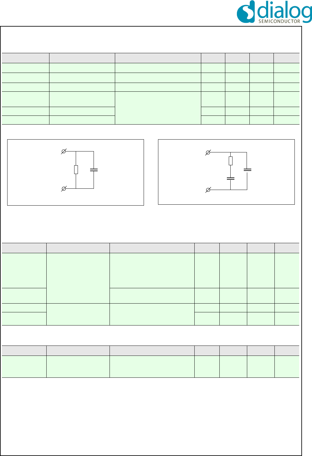
SC14CVMDECT SF Cordless Voice Module
© 2012 Dialog Semiconductor B.V. 34 July 1, 2014 v1.6
Note 19: Clipping of the outputs occurs when the VDDPA drops and the following conditions becomes true. If CLASSD_CTRL_REG[CLASSD_CLIP]
is not equal to zero then upon a programmable number of clipping occurrences a CLASSD_INT is generated:
The software can stop clipping by reducing the gain via the GENDSP:
Clipping occurs if
Table 16: LSRp/LSRn load circuits
PARAMETER DESCRIPTION CONDITIONS MIN TYP MAX UNIT
Cp1_Rl1_inf Load capacitance see Figure 30, RL1 = 30 pF
Cp1_Rl1_1k Load capacitance see Figure 30, RL1 1 k100 pF
Rl1 Load resistance 28
Cp2 Parallel load
capacitance
see Figure 31 30 pF
Cs2 Serial load capacitance 30 F
Rl2 Load resistance 600
Figure 30 Load circuit A: Dynamic loudspeaker
RL1 Cp1
LSRp
LSRn
Figure 31 Load circuit B: Piezo loudspeaker
Cs2
LSRp
LSRn
RL2
Cp2
Table 17: PAOUTp, PAOUTn outputs
PARAMETER DESCRIPTION CONDITIONS MIN TYP MAX UNIT
Vpa_4v Differential rms output
voltage between
PAOUTp and PAOUTn
Trimmed bandgap
input = 0 dBm0, 1 kHz
(Note 15)
Output low-pass filtered
CLASSD_VOUT = 0
0.985 Vrms
Vpa_6v As above
CLASSD_VOUT = 1
1.478 Vrms
Zload_pa_4v Speaker impedance,
connected between
PAOUTp and PAOUTn
With these values, the peak cur-
rents stays within the operating
range.
4
Zload_pa_6v 6
Table 18: PAOUTp, PAOUTn outputs (Note 19)
PARAMETER DESCRIPTION CONDITIONS MIN TYP MAX UNIT
Rout_pa Differential output
resistance between
PAOUTp and PAOUTn
See (Note 19) 1
peak LowPassFiltered PAOUTp PAOUTm–
VDDPA VSSPA–
-----------------------------------------------------------------------------------------------------------------------Zload
Zload Rout_pa+
-------------------------------------------
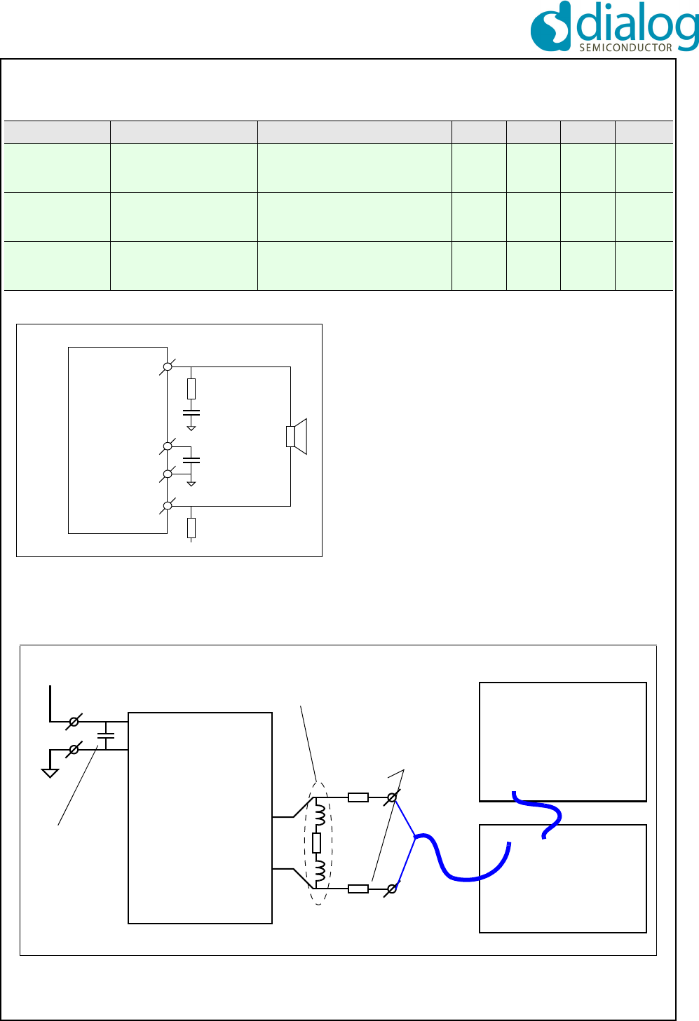
SC14CVMDECT SF Cordless Voice Module
© 2012 Dialog Semiconductor B.V. 35 July 1, 2014 v1.6
Efficiency 75% at 300 mW@2 V, 500 mW@2.5 V into a 4 transducer.
Table 19: PAOUTp, PAOUTn external components
PARAMETER DESCRIPTION CONDITIONS MIN TYP MAX UNIT
C_VDDPA Decoupling capacitor on
VDDPA
Required when Class-D is used
and guaranteed life time.
(see Figure 32)
1F
Cs_PAOUT Snubber capacitor (to
reduce ringing at
PAOUTp/n)
Required when Class-D is used
to prevent EMI and guaranteed
life time. (see Figure 32)
1nF
Rs_PAOUT Snubber resistor (to
reduce ringing at
PAOUTp/n)
Required when Class-D is used
to prevent EMI and guaranteed
life time. (see Figure 32)
1
Figure 32 Class-D external components
PAOUTp
PAOUTn
VDDPA
VSS/GND
C_VDDPA
Cs_PAOUT
Rs_PAOUT
Rs_PAOUT
Figure 33 CLASS-D amplifier measurement setup
in out
in
AP-system2, settings:
15 H
15H
4
PAOUTp
PAOUTn
VDDPA
GND (2x)
dummy load
1 F ceramic
2.5 V (= VBAT)
DUT 100
100
(models typical speaker)
bw = <10 Hz until 30 kHz
filter = A-weighting
detection = 4/s RMS
input = high-ohmic
AP AUX-0025
passive switching ampli-
fier measurement filter
resistors reduce
influence from
measurement on
DUT
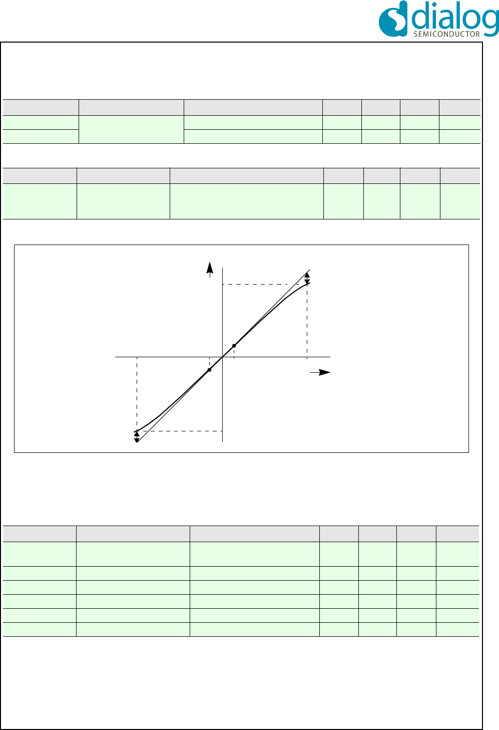
SC14CVMDECT SF Cordless Voice Module
© 2012 Dialog Semiconductor B.V. 36 July 1, 2014 v1.6
6.6 BATTERY MANAGEMENT
6.7 BASEBAND PART
Table 20: CHARGE_CTRL pin
PARAMETER DESCRIPTION CONDITIONS MIN TYP MAX UNIT
Voh_charge_ctrl Drive capability of pin
CHARGE_CTRL
sourcing 500 A1.6 V
Vol_charge_ctrl sinking 100 A0.2 V
Table 21: State of charge circuit (SoC) (Operating condition)
PARAMETER DESCRIPTION CONDITIONS MIN TYP MAX UNIT
Vsocp_socn Input voltage
between SOCp and
SOCn
With the prescribed 0.1 sense
resistor this results in the usable cur-
rent range
-100 +100 mV
Figure 34 State of charge (SOC) counter accuracy
SoC_asym_err
input current
Counter ticks/s
1000 mA
100 mA
-100 mA
-1000 mA
100 mA extrapolation
A
BSoC_sym_err: A - |B|
Table 22: Baseband specifications
PARAMETER DESCRIPTION CONDITIONS MIN TYP MAX UNIT
Fbit_uart Serial interface bit rate UART; Interface for external
microprocessor or PC
115.2 kbit/s
Fbit_flash Flash download bit rate Via UART 115.2 kbit/s
Ibat_stdby_fp Standby supply current FP application (3.3 V) 55 60 mA
Ibat_act_fp Active supply current FP application (3.3 V) 65 70 mA
Ibat_stdby_pp Standby supply current PP application (3.3 V) 4.5 6mA
Ibat_act_pp Active supply current PP application (3.3 V) 30 40 mA
SC14CVMDECT SF Cordless Voice Module
© 2012 Dialog Semiconductor B.V. 37 July 1, 2014 v1.6
6.8 RADIO (RF) PART
Standards compliancy: ETS 301 406 (former TBR6).
Table 23: Radio specifications
PARAMETER DESCRIPTION CONDITIONS MIN TYP MAX UNIT
P_Rx Receiver sensitivity BER = 0.001; TA = 25 °C -93 -92 -89 dBm
P_Rx_T Receiver sensitivity, full
temperature range
BER = 0.001;
-40 °C TA 85 °C
-87 dBm
IPL Intermodulation perform-
ance level (EN 301 406
section 4.5.7.6)
TA = 25 °C;
Pw = -80 dBm;
f = 2 channels
-35 dBm
NTP Normal transmitted power DECT: 250 mW 24 26 dBm
J-DECT: 10 mW average per
frame for each slot
23 24.5 dBm
DECT6.0: 100 mW (max
peak)
20.0 dBm
dPrfpa_T RFPA power variation, full
temperature range
-40 °C TA +85 °C 2.5 4dB
Fbit Bit rate GFSK modulation 1.152 Mbit/s
BW_Tx Transmitter bandwidth DECT GFSK;
NTP = 20 dB
1.728 MHz
Table 24: RFPA preferred settings for various power modes (PP application)
Address
(VES) Register / Parameter HPM/U
(USA)
HPM
(Europe)
HPM/J
(Japan)
0x3D RF_BBADC_CTRL_REG 0x0380 0x03A0 0x0398
0x39 RF_PA_CTRL1_REG 0x09A0 0x0CF0 0x2CE0
0x3B RF_TEST_MODE2_REG 0x0056 0x0062 0x0068
0x05 RF_PLL_CTRL2_REG[MODINDEX] 0x25 0x25 0x23
0x23 Upper RSSI threshold 0x2C N/A 0x28
0x24 Lower RSSI threshold 0x22 N/A 0x1E
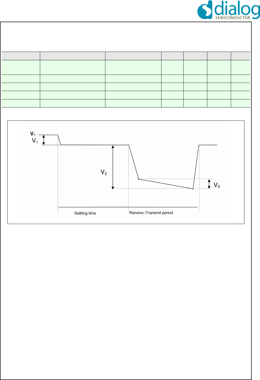
SC14CVMDECT SF Cordless Voice Module
© 2012 Dialog Semiconductor B.V. 38 July 1, 2014 v1.6
6.9 RF POWER SUPPLY
Table 25: Requirements for linear supply regulator
PARAMETER DESCRIPTION CONDITIONS MIN TYP MAX UNIT
VBAT IN Voltage at VBAT SW Unloaded VB
Loaded VB-V1-V2-V3
2.1 33.45 V
V1Settling time I = 50 mA 20 mV
V2Receive period I = 130 mA 100 mV
V2Transmit period I = 550 mA 200 mV
V3Drop during transmit 25 mV
Figure 35 RF power supply
B
SC14CVMDECT SF Cordless Voice Module
© 2012 Dialog Semiconductor B.V. 39 July 1, 2014 v1.6
6.10 RF CHANNEL FREQUENCIES
RF setting values must be followed according to
AN-D-204 when DECT country mode was changed.
Table 26: RF frequencies and channel numbers
Frequency
(MHz)
DECT
CH
J-DECT
CH
DECT6.0
CH
1881.792 9
1883.520 8
1885.248 7
1886.976 6
1888.704 5
1890.432 4
1892.160 3
1893.888 2
1895.616 1 1
1897.344 0 0
1899.072 10
1900.800 11
1902.528 12
1921.536 4
1923.264 3
1924.992 2
1926.720 1
1928.448 0

SC14CVMDECT SF Cordless Voice Module
© 2012 Dialog Semiconductor B.V. 40 July 1, 2014 v1.6
7.0 Design guidelines
This section describes the software and hardware con-
siderations to be taken into account when designing
the target application.
The SC14CVMDECT SF can be used standalone or
next to an MCU that controls the module. In case the
module is used standalone the application will be
stored in its on-board Flash. In total 324 kB of Flash is
available for this purpose.
Applications can be developed with the Athena soft-
ware development environment (see reference [3]).
7.1 APPLICATION SOFTWARE FOR PP
In a PP application the following software tasks must
be handled by the MCU or within the module itself:
• UART communication (external microprocessor
only)
• PP MMI
• Display interface (optional)
• Keyboard interface (optional)
• Battery Charge interface (optional)
• Audio handling
• Tone / Melodies handling
For control commands see document reference [2].
UART communication
The UART communication is the main control interface
of the SC14CVMDECT SF.
PP MMI
The MMI state machine must handle the call setup and
call termination on the PP.
Display Interface
The MCU / PP handles the display interface including
the display driver.
Keyboard Interface
The MCU/ PP handles the keyboard interface including
the keyboard driver.
Audio handling
The Application Software state machine must control
when to open and close the audio. The headset plug-in
detection must handled by the host, and a status is
send to the PP MMI from the PP stack software. The
PP MMI must handle the volume control.
Headset detection boundaries can be adjusted in VES.
When headset indication is received from the PP
Headset detection logic, the Application Software can
decide if audio should be switched to the headset and
sends a request to the PP stack software.
The PP audio handling basically consists of 4 audio
modes (see Figure 14):
1. Idle (Alert) mode
2. Earpiece mode
3. Handsfree mode (Speakerphone)
4. Headset mode
Shifting between modes is done through the API.
Tone handling
The Application Software state machine must control
when to play tones and the volume setting. Custom
melodies can be defined in the VES.
7.2 APPLICATION SOFTWARE FOR FP
In an FP application the following software tasks must
be handled by the MCU or within the module itself:
• UART communication (external microprocessor
only)
•FP MMI
• Display interface (optional)
• Keyboard interface (optional)
• Audio handling
• Tone / Melodies handling
For control commands see document reference [1].
UART communication
The UART communication forms the basic of the FP
operation because via this interface the
SC14CVMDECT SF is controlled.
FP MMI
The MMI state machine must handle the call setup and
call termination on the FP.
Display interface
The MCU/ FP handles the display interface including
the display driver.
Keyboard interface
The MCU/ FP handles the keyboard interface including
the keyboard driver.
Audio handling
The Application Software state machine must control
when to open and close the audio. The FP MMI must
handle the volume control.
Tone handling
The Application Software state machine must control
when to play tones and the volume setting. Custom
melodies can be defined in VES.
7.3 HARDWARE DESIGN GUIDELINES
Within this section general design guidelines for
SC14CVMDECT SF FP and PP applications are given.
7.3.1 Circuit design guidelines
For a reference schematic refer to the SC14CVMDECT
SF reference kit. With the reference kit package a non-
cost optimised reference design is presented.
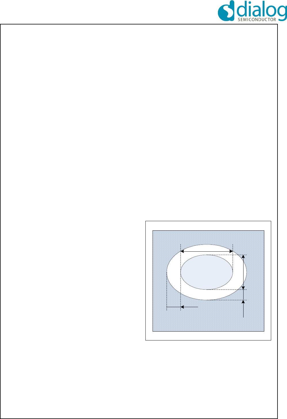
SC14CVMDECT SF Cordless Voice Module
© 2012 Dialog Semiconductor B.V. 41 July 1, 2014 v1.6
For a FP hardware design the following hardware parts
will be needed besides the SC14CVMDECT SF:
• Supply voltage
• Battery charge
• LED and buttons
• Audio:
• Headset
• External PCM device.
For a PP hardware design the following hardware parts
will be needed besides the SC14CVMDECT SF:
• Power
• Battery Charger
• Audio:
• Microphone
• Earpiece
• Speaker
• Headset
7.3.2 PCB Design Guidelines
• Because of the presence of the digital radio fre-
quency burst with 100 Hz time division periods (TDD
noise), supply ripple and RF radiation, special atten-
tion is needed for the power supply and ground PCB
layout.
• Power supply considerations
Both high and low frequency bypassing of the supply
line connections should be provided and placed as
close as possible to the SC14CVMDECT SF. In
order to get the best overall performance for both FP
and PP applications, a number of considerations for
the PCB has to be taken into account.
• Make angle breaks on long supply lines to avoid
resonance frequencies in respect to DECT fre-
quencies. Maximum 8 cm before an angle break
is recommended.
• Supply lines should be placed as far as possible
away from sensitive audio circuits. If it is neces-
sary to cross supply lines and audio lines, it
should be done with right angles between supply
and audio lines/circuits (microphone, ear-speaker,
speakerphone, etc.)
• Ground plane considerations
In order to achieve the best audio performance
and to avoid the influence of power supply noise,
RF radiation, TDD noise and other noise sources,
it is important that the audio circuits on both FP
and PP applications boards are connected to the
VREFM pin (analog ground: AGND, see Figure
38) on the SC14CVMDECT SF with separate nets
in the layout.
It is advised to provide the following audio circuits
with separate ground nets connected to the
VREFM pin:
• Microphone(s)
• Headset microphone and speaker
• Speakerphone (signal grounds)
Depending on the layout it may also be necessary to
bypass a number of the audio signals listed above to
avoid humming, noise from RF radiation and TDD
noise with. It is also important to choose a microphone
of appropriate quality with a high RF immunity (with
built-in capacitor).
• ESD performance
Besides TDD noise, the ESD performance is impor-
tant for the end-application. In order to achieve a
high ESD performance supply lines should be
placed with a large distance from charging terminals,
display, headset connector and other electrical ter-
minals with direct contact to the ESD source.
On a two-layer PCB application it is important to
keep a simulated one layer ground. With a stable
ground ESD and TDD noise performance will always
improve.
• Clearance around test patterns
Pin number 81 to 88 are used for production test
purposes. In order to avoid any interference or dis-
turbance the area around these signal pins must be
kept clear of any signal and/or GND. The recom-
mended clearance is at least 1 mm as shown in Fig-
ure 36.
Figure 36 Clearance around test patterns
Test
pattern
0.9mm
0.6mm1.0mm
1.0mm
GND Pattern
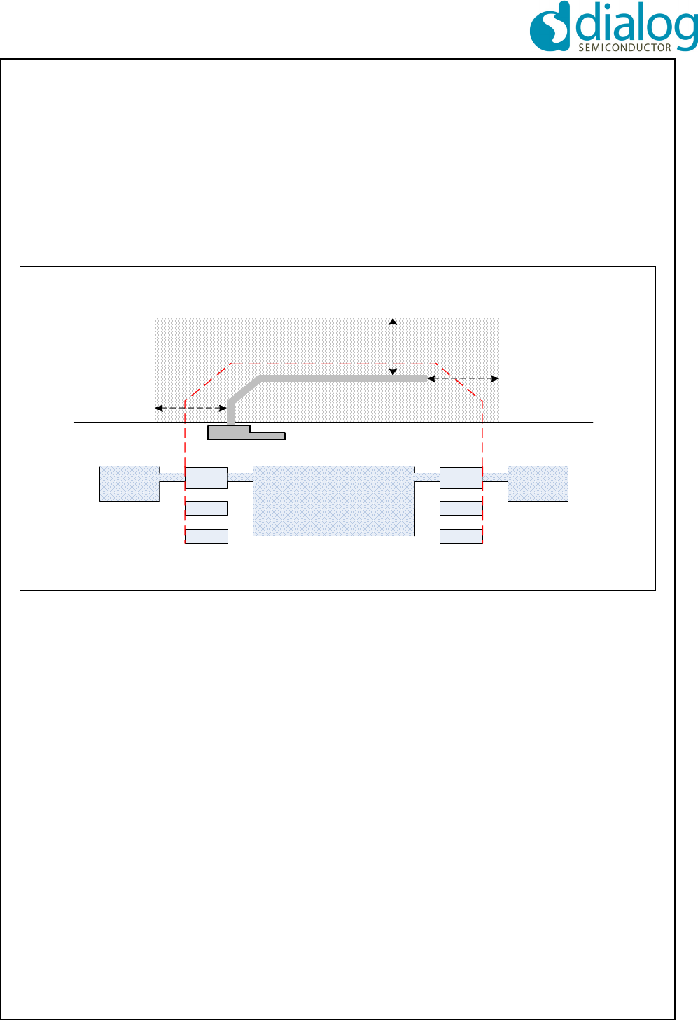
SC14CVMDECT SF Cordless Voice Module
© 2012 Dialog Semiconductor B.V. 42 July 1, 2014 v1.6
7.4 MODULE PLACEMENT ON THE MAIN BOARD
In order to ensure FCC compliance, proper coverage
and to avoid detuning of the antennas, it is required to
place the module free on the main board in relation to
other surrounding materials.
Keep a distance of at least 10 mm from the antenna
elements to conducting objects and at least 5 mm to
non-conducting objects.
Keep in mind that electrical shielding objects, even
partly surrounding the antennas, will normally cause a
significant degradation of the coverage.
Place the module at the edge of the main-board as
shown in Figure 37.
If the module has to be placed away from the edge of
the main board, then avoid conducting areas in front of
the antennas and make a cut-out in the main board
underneath the antennas as shown in the figure.
Keep solid ground on layer 2 out to the edges of the
main board as shown in the figure.
7.5 PATTERN FOR PIN 79 ON THE MAIN BOARD
The copper pattern for pin 79 on the main board is very
important because it is part of the internal antenna of
the module. It is used to extend the internal antenna for
optimum RF performance.
The PCB pattern shown in Figure 41 under “pads C”
for pin 79 on the main board was used during module
certification.
7.6 PRECAUTIONS REGARDING UNINTENDED
COUPLING
The SC14CVMDECT SF includes the internal antenna,
so by integration on the main board precautions shall
be taken in order to avoid any kind of coupling from the
main board to the RF part of the module.
If there is any doubt about this, a brief radio test should
be performed.
Figure 37 Module placement on the main board (top view)
178
No PCB area
2
376
77
GND
GND GND
79 Main boardModule
antenna extension
> 10 mm
> 10 mm
> 10 mm
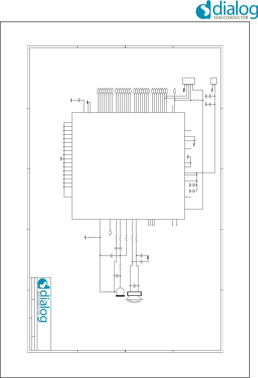
SC14CVMDECT SF Cordless Voice Module
© 2012 Dialog Semiconductor B.V. 43 July 1, 2014 v1.6
8.0 Example Application Diagram
Figure 38 Reference diagram example
5
5
4
4
3
3
2
2
1
1
D D
C C
B B
A A
AGND
UTX
URX
P0[2]
P0[3]
P0[4]
P0[5]
P0[6]
P0[7]
P1[0
P1[1]
P1[2]
P1[3]
P1[4]
P1[5]
PON
CHARGE
P2[0]
P2[1]
P2[2]
P2[3]
P2[4]
P2[5]
P2[6]
P2[7]
MICh
PAOUTn
PAOUTp
P3[2]
P3[3]
P3[4]
P3[5]
P3[6]
P3[7]
JTAG
Title :
Doc. Nr. Rev:
Date: Sheet: of
Dialog Semiconductor .
Het Zuiderkruis 53
5215 MV 's-Hertogenbosch
tel. (+31) 73 6408822
fax. (+31) 73 6408823
Designer: 0.1
SC14CVMDECT_SF01_RD
11Wednesday, November 28, 2012
F v D
<OrgName>
Title :
Doc. Nr. Rev:
Date: Sheet: of
Dialog Semiconductor .
Het Zuiderkruis 53
5215 MV 's-Hertogenbosch
tel. (+31) 73 6408822
fax. (+31) 73 6408823
Designer: 0.1
SC14CVMDECT_SF01_RD
11Wednesday, November 28, 2012
F v D
<OrgName>
Title :
Doc. Nr. Rev:
Date: Sheet: of
Dialog Semiconductor .
Het Zuiderkruis 53
5215 MV 's-Hertogenbosch
tel. (+31) 73 6408822
fax. (+31) 73 6408823
Designer: 0.1
SC14CVMDECT_SF01_RD
11Wednesday, November 28, 2012
F v D
<OrgName>
R9
1K
C4
DNA
R2
0R
LSR1
1
1
2
2
R7
0R
SC14CVMDECT SF01
U1
SC14WSMDATA_SF01
P1[2]/INT2/SK
36
VBATSW 62
P0[4]/SPI_EN
43
RSTn
52
CP_VOUT1
26
P1[5]/INT5/RDI/VDDE
33
P2[6]WTF_IN
39
P0[1]/URX
47
VBATIN 63
P3[0]/PAOUTn/DP0
27
P2[7]/BXTAL
32
P1[4]/INT4/TDOD
34
P1[1]/INT1/LE
37
P0[0]/UTX
48
JTAG
53
P3[1]/PAOUTp/DP1
24
P1[6] / PON
29
P1[7] / CHARGE
23
P2[4]/SCL1/PCM_DO/DP3
55
VDDOUT 61
P2[5]/PCM_FSC/SF
54
VDDPA 25
CHARGE_CTRL 22
P0[7]/SPI_DI/PWM1
40
SOCp 17
P1[0]/INT0/ADC1
16
ULP_PORT
31
ULP_XTAL
30
P0n 4
P2[3]/SDA1/PCM_DI/DP2
56
P1[3]/INT3/SIO
35
P0[6]/SPI_DO
41
LSRn 13
P3[3]/ADC0
15
DC_CTRL 21
VREFm 11
LSRp 12
P3[7]/RINGp
66
DC_SENSE 19
DC_I 20
P2[2]/PCM_CLK/CLK100
57
RFP0n 5
MICh 10
P3[5]/RINGING/RINGOUT
68
RFP0 3
P2[1]/ECZ2/PWM1/LED4
58
VREFp 7
MICp/CIDINn 8
P3[2]/CIDINp
65
P3[6]RINGn
67
P3[4]/PARADET
69
P2[0]/ECZ1/PWM0/LED3
59
RF0 75
MICn/CIDOUT 9
P0 2
RF1 73
P0[5]/SPI_CLK
42
VBATIN 64
P0[3]/URX2/SCL2
44 P0[2]/UTX2/SDA2
46
GND
1
GND
14
GND
38
GND
49
GND
50
GND
60
GND
51
GND
6
SOCn/GND 18
GND
28
GND
45
GND
70
GND
71
GND
72
GND
74
GND
76
GND
77
GND
78
GND
80
C13
1uF
R5
1K
MIC1
1
1
2
2
C9
DNA
C12
10pF
+
C11
22uF
R3
0R
R6
10R
C8
0,.1uF
R1
0R
C5
DNA
C15
10pF
J1
1
2
C3
1uF
C6
DNA
C10
DNA
J2
1
2
3
4
5
R8
1K
R4
0R
C7
0,.1uF
internal

SC14CVMDECT SF Cordless Voice Module
© 2012 Dialog Semiconductor B.V. 44 July 1, 2014 v1.6
9.0 Notices to OEM
The end product has to be certified again if it has
been programmed with other software than Dialog
standard software stack for portable part and/or
uses one or two external antenna(s).
9.1 FCC REQUIREMENTS REGARDING THE END
PRODUCT AND THE END USER.
The end product that the module is integrated into must
be marked as follows:
“Contains Transmitter Module FCC ID: Y82-SC14S /
IC: 9576A-SC14S”
The literature provided to the end user must include the
following wording:
FCC compliance statement
This device complies with Part 15 of the FCC Rules for
only portable part.
Operation is subject to the following two conditions: (1)
this device may not cause harmful interference, and (2)
this device must accept any interference received,
including interference that may cause undesired opera-
tion of the device.
Module transmetteur ID IC: 9576A-SC14S.
Son fonctionnement est soumis aux deux conditions
suivantes: (1) cet appareil ne doit pas causer d’interfé-
rences nuisibles et (2) appareil doit accepter toute
interférence reçue, y compris les interférences qui peu-
vent perturber le fonctionnement.
Changes or modifications to the equipment not
expressly approved by the Party responsible for com-
pliance could void the user's authority to operate the
equipment.
NOTE: This equipment has been tested and found to
comply with the limits for a Class B digital device, pur-
suant to Part 15 of the FCC Rules. These limits are
designed to provide reasonable protection against
harmful interference in a residential installation.
This equipment generate, uses and can radiate radio
frequency energy and, if not installed and used in
accordance with the instructions, may cause harmful
interference to radio communications. However, there
is no guarantee that interference will not occur in a par-
ticular installation.
If this equipment does cause harmful interference to
radio or television reception, which can be determined
by turning the equipment off and on, the user is
encouraged to try to correct the interference by one or
more of the following measures:
• Reorient or relocate the receiving antenna
• Increase the separation between the equipment and
receiver
• Connect the equipment into an outlet on a circuit dif-
ferent from that to which the receiver is connected.
• Consult the dealer or an experienced radio/TV tech-
nician for help.
Privacy of communications may not be ensured when
using this phone.
9.2 INDUSTRY CANADA REQUIREMENTS
REGARDING THE END PRODUCT AND THE END
USER
The host device shall be properly labelled to identify
the modules within the host device. The Industry Can-
ada certification label of a module shall be clearly visi-
ble at all times when installed in the host device,
otherwise the host device must be labelled to display
the Industry Canada certification number of the mod-
ule, preceded by the words "Contains transmitter mod-
ule", or the word "Contains", or similar wording
expressing the same meaning, as follows:
Contains transmitter module IC: 9576A-SC14S
L'appareil hôte doit être étiqueté comme il faut pour
permettre l'identification des modules qui s'y trouvent.
L'étiquette de certification d'Industrie Canada d'un
module donné doit être posée sur l'appareil hôte à un
endroit bien en vue en tout temps. En l'absence d'éti-
quette, l'appareil hôte doit porter une etiquette donnant
le numéro de certification du module d'Industrie Can-
ada, précédé des mots " Contient un module d'émis-
sion ", du mot " Contient " ou d'une formulation
similaire exprimant le même sens, comme suit :
Contient le module d'émission IC: 9576A-SC14S
This device complies with Industry Canada licence-
exempt RSS standard(s). Operation is subject to the
following two conditions: (1) this device may not cause
interference, and (2) this device must accept any inter-
ference, including interference that may cause unde-
sired operation of the device.
Le présent appareil est conforme aux CNR d'Industrie
Canada applicables aux appareils radio exempts de
licence. L'exploitation est autorisée aux deux condi-
tions suivantes : (1) l'appareil ne doit pas produire de
brouillage, et (2) l'utilisateur de l'appareil doit accepter
tout brouillage radioélectrique subi, même si le brouil-
lage est susceptible d'en compromettre le fonctionne-
ment.
CAN ICES-3 (B)/NMB-3(B)

SC14CVMDECT SF Cordless Voice Module
© 2012 Dialog Semiconductor B.V. 45 July 1, 2014 v1.6
9.3 PRECAUTIONS REGARDING UNINTENDED
COUPLING
Integration on the main board precautions shall be
taken in order to avoid any kind of
coupling from the main board to the RF part of the
module. If there is any doubt about this, a radio short
test should be performed.
9.4 END APPLICATION APPROVAL
The module is intended to be used in an end applica-
tion. Type approval concerning the end product, except
for the module, should off cause be done. Please con-
tact a test-house in order to clarify what is needed.
9.5 SAFETY REQUIREMENTS
This section provides of an overview of the safety
requirements you must adhere to when working with
the Cordless Voice Module SC14CVMDECT SF.
• The specific external power supply for the Cordless
Voice Module SC14CVMDECT SF has to fulfil the
requirements according to clause 2.5 (Limited power
source) of this standard EN 60950-1:2006.
• Interconnection circuits shall be selected to provide
continued conformance to the requirements of
clause 2.2 for SELV (Safety Extra Low Voltage) cir-
cuits according to EN 60950-1:2006 after making
connections.
• Interface type not subjected to over voltages (i.e.
does not leave the building).
• Requirements additional to those specified in this
standard may be necessary for:
• Equipment intended for operation in special envi-
ronments (for example, extremes of temperature,
excessive dust, moisture or vibration, flammable
gases and corrosive or explosive atmospheres).
• Equipment intended to be used in vehicles, on
Board ships or aircraft, in tropical countries or at
altitudes greater than 2000 m.
• Equipment intended for use where ingress of
water is possible.
• Installation by qualified personnel only!
• The product is a component intended for installation
and use in complete equipment. The final accept-
ance of the component is dependent upon its instal-
lation and use in complete equipment.
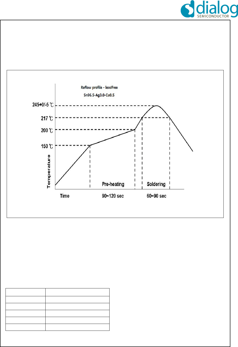
SC14CVMDECT SF Cordless Voice Module
© 2012 Dialog Semiconductor B.V. 46 July 1, 2014 v1.6
10.0 Package information
10.1 SOLDERING PROFILE
The SC14CVMDECT SF should be soldered using a
standard reflow soldering profile and lead free solder
paste as shown below. Adjustments to the profile may
be necessary depending on process requirements.
10.2 MOISTURE SENSITIVITY LEVEL (MSL)
The MSL is an indicator for the maximum allowable
time period (floor life time) in which a moisture sensi-
tive plastic device, once removed from the dry bag, can
be exposed to an environment with a maximum tem-
perature of 30°C and a maximum relative humidity of
60% RH. before the solder reflow process.
The SC14CVMDECT SF is qualified to MSL 3.
Figure 39 Reflow profile
MSL Level Floor Life Time
MSL 4 72 hours
MSL 3 168 hours
MSL 2A 4 weeks
MSL 2 1 year
MSL 1 Unlimited at 30°C/85%RH
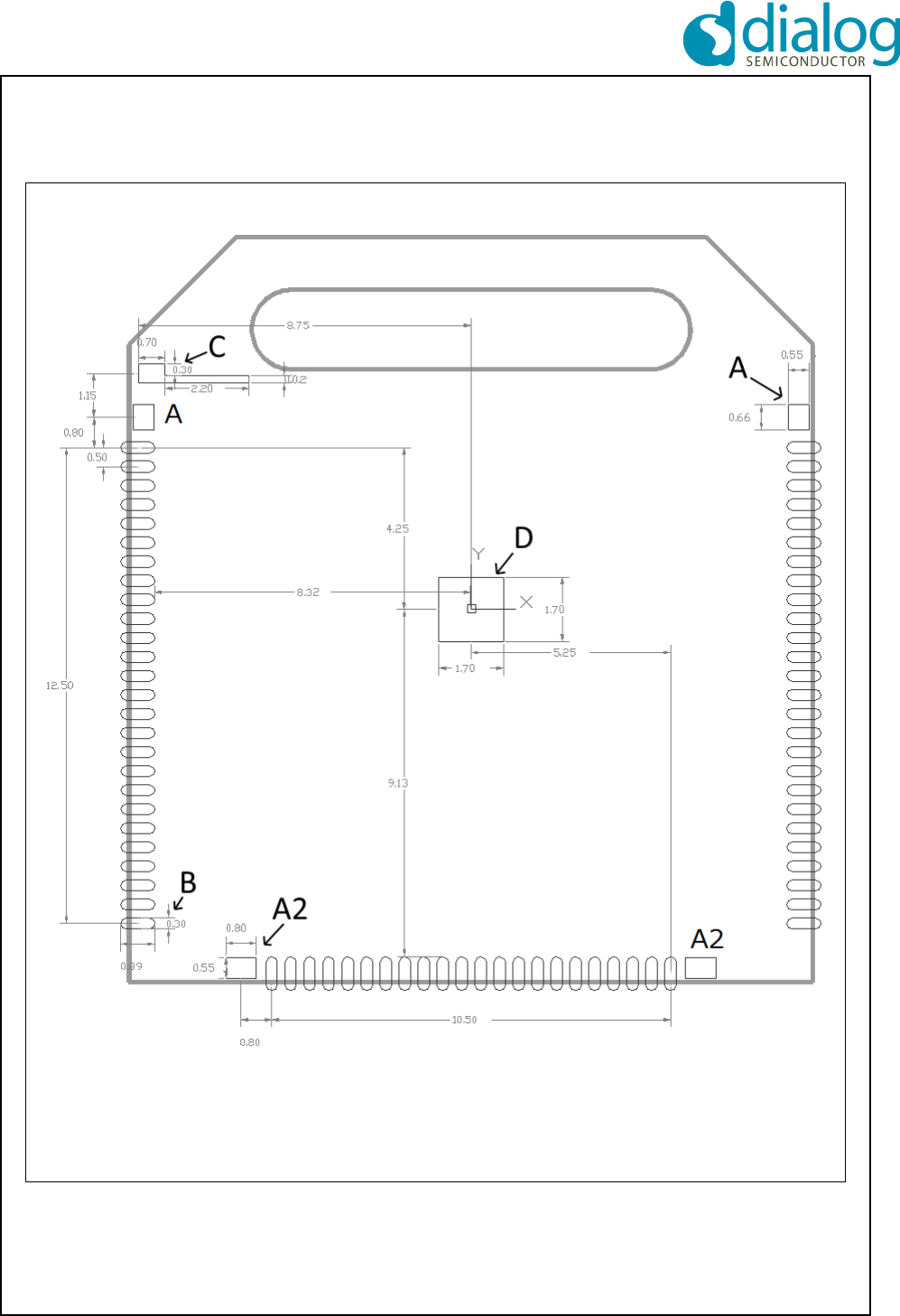
SC14CVMDECT SF Cordless Voice Module
© 2012 Dialog Semiconductor B.V. 47 July 1, 2014 v1.6
10.3 COPPER PAD, SOLDER OPENING AND STEN-
CIL
For the stencil a thickness of 0.122 mm is recom-
mended. Recommended copper pad, solder mask
opening and stencil are shown below.
Figure 40 Pad dimensions
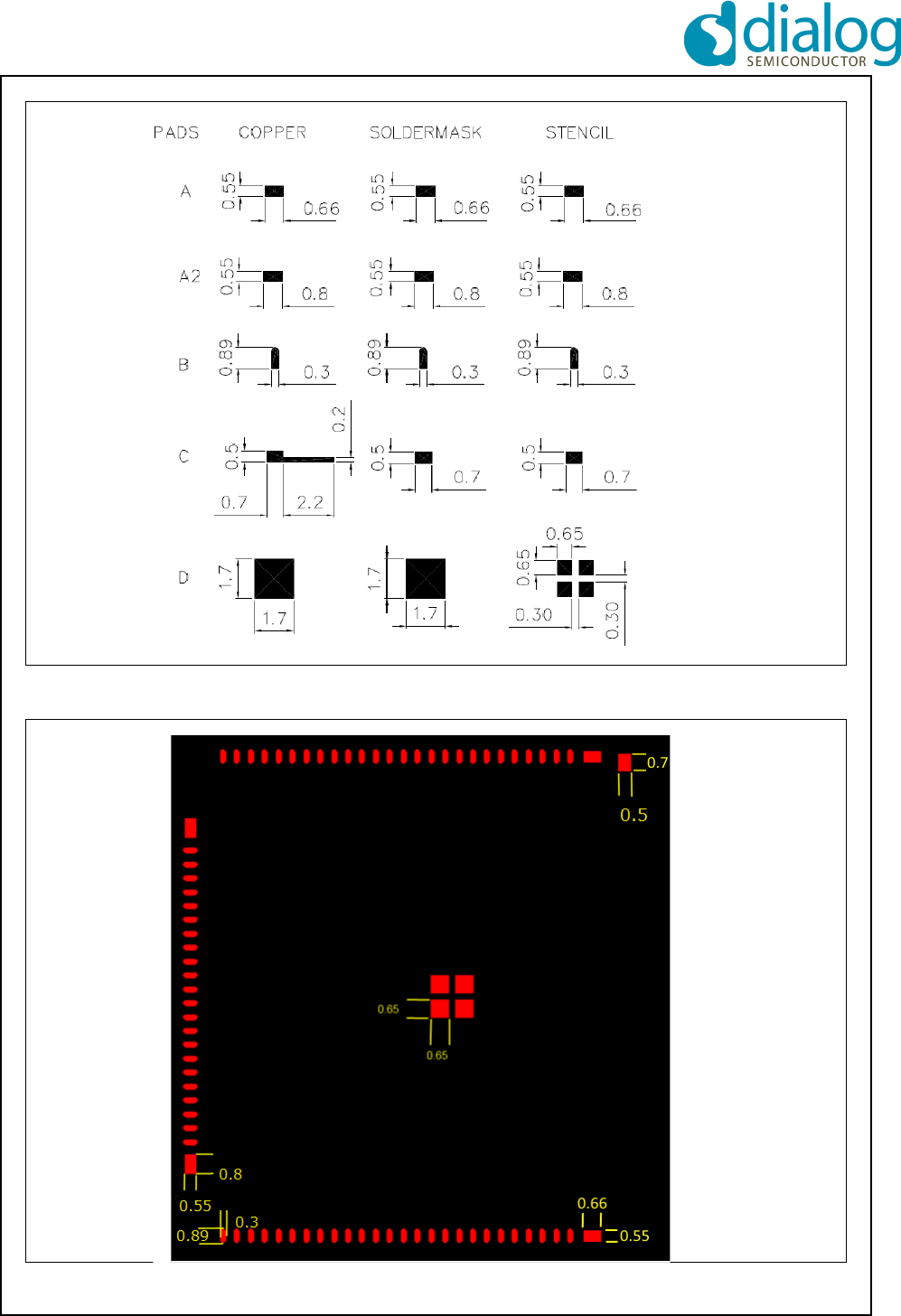
SC14CVMDECT SF Cordless Voice Module
© 2012 Dialog Semiconductor B.V. 48 July 1, 2014 v1.6
Figure 41 Copper pad, Solder mask opening and Stencil
Figure 42 Solder stencil
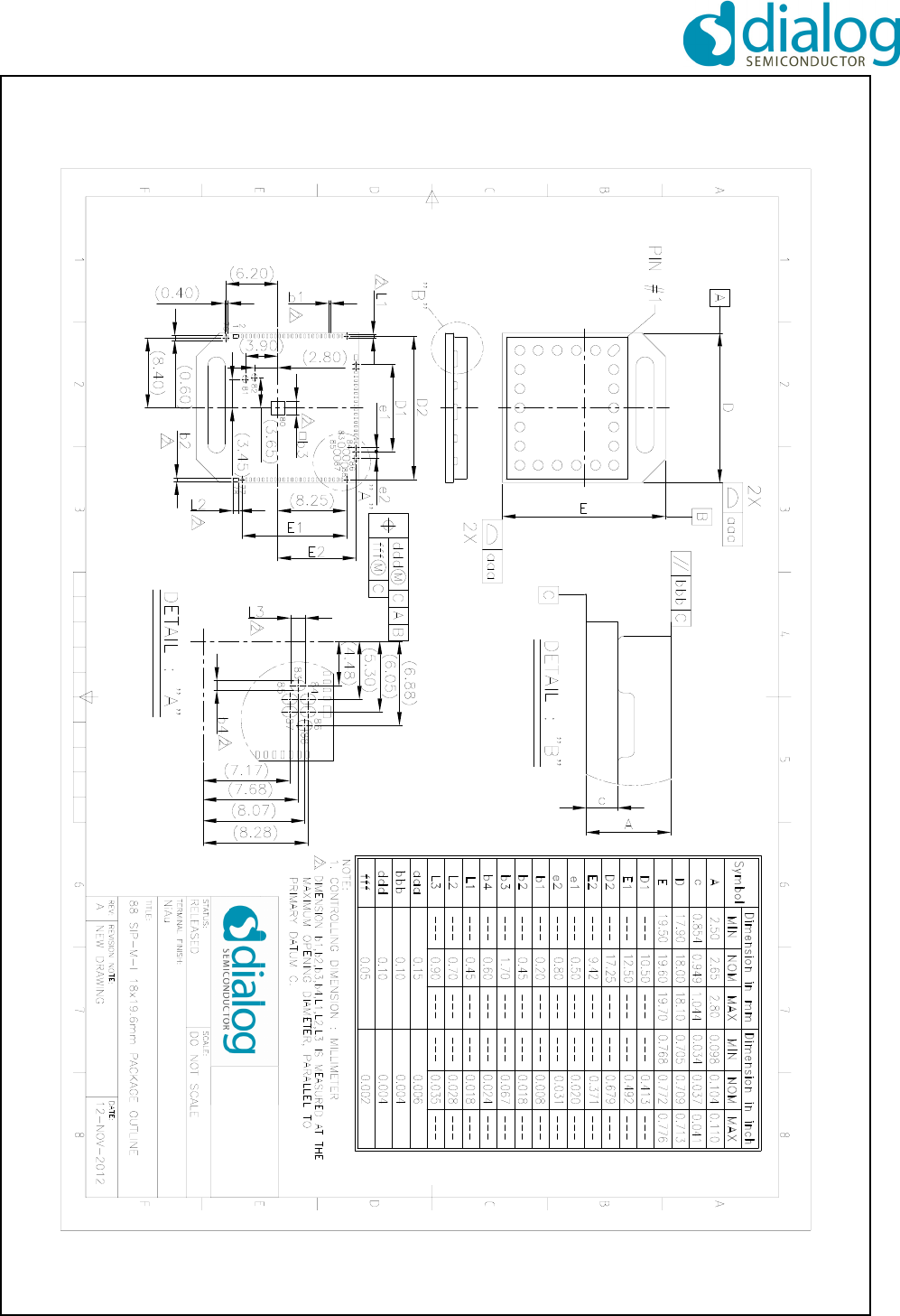
SC14CVMDECT SF Cordless Voice Module
© 2012 Dialog Semiconductor B.V. 49 July 1, 2014 v1.6
10.4 MECHANICAL DIMENSIONS
Figure 43 Package outline drawing

SC14CVMDECT SF Cordless Voice Module
© 2012 Dialog Semiconductor B.V. 50 July 1, 2014 v1.6
11.0 Revision history
Jul1, 2014 v1.6:
• Changed maximum RF output power for DECT 6.0
Apr16, 2014 v1.5
• Added an explanation for RF1 on 4.13
Feb 11, 2014 v1.4
• Correct 10.3Copper pad, solder openinG and
STENCIL47
Jan 31, 2014 v1.3
• Update 10.3Copper pad, solder openinG and
STENCIL47
Nov 8, 2013 v1.2:
• Added section “9.2 INDUSTRY CANADA
REQUIREMENTS REGARDING THE END PROD-
UCT AND THE END USER”
Sept 12, 2013 v1.1:
• Ordering code for tray version corrected.
• Ordering code for tape-on-reel version removed.
July 9, 2013 v1.0: Initial version

SC14CVMDECT SF Cordless Voice Module
© 2012 Dialog Semiconductor B.V. 51 July 1, 2014 v1.6
Product Status Definitions
Dialog Semiconductor reserves the right to make changes without notice to any products herein to improve reliabil-
ity, function or design. Dialog Semiconductor does not assume any liability arising out of the application or use of
any product or circuit described herein; neither does it convey any license under its patent rights, nor the right of oth-
ers.
Datasheet Status Product Status Definition
Advance Information Formative or in Design This data sheet contains the design specifications for prod-
uct development. Specifications may change in any manner
without notice.
Preliminary First Production This data sheet contains preliminary data. Supplementary
data will be published at a later date. Dialog Semiconductor
reserves the right to make changes at any time without
notice in order to improve design and supply the best possi-
ble product.
No Identification Noted Full production This data sheet contains final specifications. Dialog Semi-
conductor reserves the right to make changes at any time
without notice in order to improve design and supply the best
possible product.
Obsolete Not in Production This data sheet contains specifications on a product that has
been discontinued by Dialog Semiconductor. The data-sheet
is printed for reference information only.
Life Support Policy
DIALOG’S PRODUCTS ARE NOT AUTHORIZED FOR USE AS CRITICAL COMPONENTS IN LIFE SUPPORT
DEVICES OR SYSTEMS WITHOUT THE EXPRESS WRITTEN APPROVAL OF THE PRESIDENT AND GENERAL
COUNCIL OF DIALOG SEMICONDUCTOR. As used herein:
1. Life support devices or systems are devices or
systems which,
(a) are intended for surgical implant into the
body, or (b) support or sustain life, and whose
failure to perform, when properly used in accord-
ance with instructions for use provided in the
labelling, can be reasonably expected to result
in a significant injury to the user.
2. A critical component is any component of a life
support device or system whose failure to per-
form can be reasonably expected to cause the
failure of the life support device or system, or to
affect its safety or effectiveness.
Germany Headquarters
Dialog Semiconductor GmbH
Phone: +49 7021 805-0
United Kingdom
Dialog Semiconductor (UK) Ltd
Phone: +44 1793 757700
The Netherlands
Dialog Semiconductor B.V.
Phone: +31 73 640 88 22
Dialog Semiconductor does not assume any responsibility for use of any circuit described, no circuit patent licenses are implied, and Dialog
reserves the right, at any time without notice, to change said circuitry or specifications.
Contacting Dialog Semiconductor
RoHS Compliance
Dialog Semiconductor complies to European Directive 2001/95/EC and from 2 January 2013 onwards to European
Directive 2011/65/EU concerning Restriction of Hazardous Substances (RoHS/RoHS2).
Dialog Semiconductor’s statement on RoHS can be found on the customer portal http:/portal.dialog-semiconduc-
tor.com. RoHS certificates from our suppliers are available on request.
North America
Dialog Semiconductor Inc.
Phone: +1 408 727 3200
Japan
Dialog Semiconductor K. K.
Phone: +81 3 5425 4567
Taiwan
Dialog Semiconductor Taiwan
Phone: +886 226 580 388
Singapore
Dialog Semiconductor Singapore
Phone: +65 64845419
China
Dialog Semiconductor China
Phone: +852 2607 4271
Korea
Dialog Semiconductor Korea
Phone: +82 2 569 2301