Dialog Semiconductor SC14S DECT Module User Manual SC14CVMDECT SF01 V16
Dialog Semiconductor BV DECT Module SC14CVMDECT SF01 V16
UserManual.wiki
>
Dialog Semiconductor
>
SC14S User Manual
>
user manual CVMDECT
Contents
1.
user manual CVMDECT
2.
user manual SPNODE
3.
Rev_User Manual_68-2959-01_Bx_101217.pdf
user manual CVMDECT
Navigation menu
Upload a User Manual
Namespaces
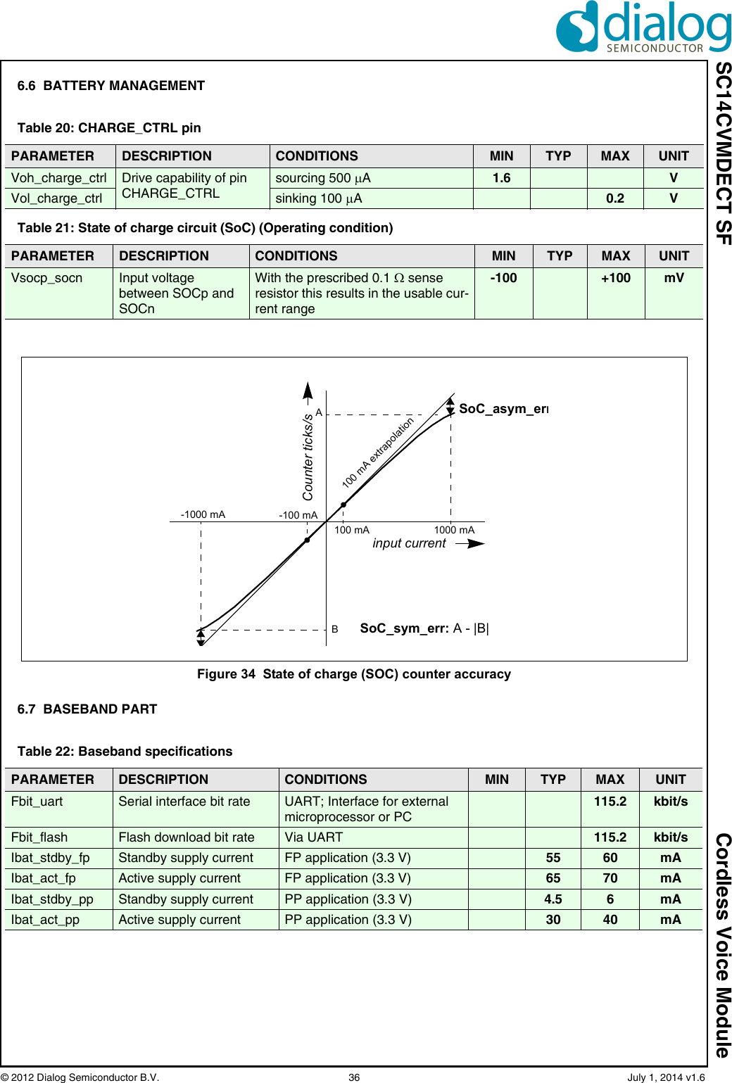
Wiki Guide
HTML
PDF
Info
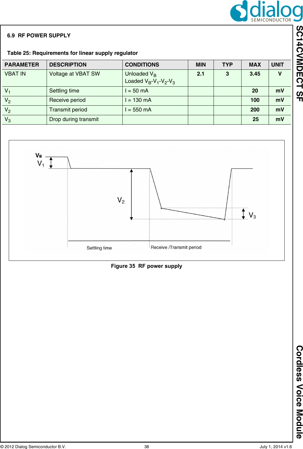
Views
User Manual
Discussion / Help
Navigation
![SC14CVMDECT SF Cordless Voice Module© 2012 Dialog Semiconductor B.V. 4 July 1, 2014 v1.61.0 Connection diagramFigure 1 Connection diagram (top view, leads face down)Order numbers:SC14CVMDECT SF01T (tray, MPQ = 600 pcs) up to 6 PPs can be registered.1232221201918171615141312111098765432274948474645444342414039383736353433323130292826252472505152535455565758596061626364656667686970717980GNDPARADET/P3[4]P2[0]/ECZ1/PWM0/LED3GNDTP1RINGOUT/RINGING/P3[5]GNDRFP0P0GNDGNDADC0/P3[3]LSRn/LINEOUT/AGNDLSRp/LINEOUT/AGNDVREFmMICn/CIDOUTMICp/CIDINnVREFpMICh/LINEINCIDINp/P3[2]RINGp/P3[7]RINGn/P3[6]DC_IDC_SENSESOCnSOCpADC1/INT0/P1[0]DC_CTRLVDDE/RDI/INT5/P1[5]ULP_PORTULP_XTALPON/P1[6]CP_VOUT1GNDDP0/PAOUTn/P3[0]VDDPADP1/PAOUTp/P3[1]CHARGE/P1[7]CHARGE_CTRLVBATSWVBATINVBATINVDDOUTGNDSIO/INT3/P1[3]TDOD/INT4/P1[4]BXTAL/INT7/P2[7]SK/INT2/P1[2]LE/INT1/P1[1]P0[7]/PWM1SPI_DIP0[6]/SPI_DOGNDWTF_IN/P2[6]P0[4]/SPI_ENP0[3]/SCL2/URX2P0[5]/SPI_CLKP0[2]/SDA2/UTX2P0[1]/PWM0/URXP0[0]/UTXGNDRSTnJTAGSF/P2[5]/PCM_FSCDP3/P2[4]/SCL1/PCM_DODP2/P2[3]/SDA1/PCM_DICLK100/P2[2]/PCM_CLKP2[1]/ECZ2/PWM1/LED4RFP0nP0nRF1GNDRF0GNDGNDGNDGNDGND787776757473GNDGNDGND8182838487888586](https://usermanual.wiki/Dialog-Semiconductor/SC14S.user-manual-CVMDECT/User-Guide-2324864-Page-4.png)
![SC14CVMDECT SF Cordless Voice Module© 2012 Dialog Semiconductor B.V. 5 July 1, 2014 v1.61.1 PIN DESCRIPTIONTable 1: Pin descriptionPinModule Pin name(Note 1)In/OutIoutDrive(mA)Reset State (Note 2)Description1GND - - -Ground2 P0 O 8 Hi-Z Control port for FAD. See 4.133 RFP0 O 8 Hi-Z Control port for FAD. See 4.134 P0n O 8 Hi-Z Control port for FAD. See 4.135 RFP0n O 8 Hi-Z Control port for FAD. See 4.136GND - - -Ground7 VREFp O - I Positive microphone supply voltage8 MICp I - I Positive microphone input9 MICn I - I Negative handset microphone input10 MICh I - I Headset microphone input with fixed input protection11 VREFm - - - Negative microphone reference (star point), connect to GND.12 LSRp O - O Positive loudspeaker output13 LSRn O - O Negative loudspeaker output14 GND - - - Ground15 P3[3] IO 8 I I/O Port16 P1[0] IO 2 I-PU I/O Port17 SOCp I - I Battery state of charge positive input.Connect to GND if not used. See 4.918 SOCn I - I Battery state of charge negative input. Star point connected to the SOC resistor. Connect to GND if not used. See 4.919 DC_SENSE I I Voltage sense input. Connect to GND if not used.20 DC_I I I Current sense input of DC/DC converter. Connect to GND if not used21 DC_CTRL O 2 O-0 Switching clock for the DC/DC converter.22 CHARGE_CTRL O 1 O-0 Charge control pin.Leave unconnected if not used. See 4.923 CHARGE I - I-PD(270k fixed pull-down)Charger connected indication. Switches on the device if voltage > 1.5 V. Must be connected to charger via resistor R > (Vcharger_max-3 V)/10 mA (round to next largest value in range). See 4.924 PAOUTp IO 500 O-0 (5k fixed pull-down)CLASSD loudspeaker positive outputs25 VDDPA I - - CLASSD Audio Amplifier supply voltage up to 3.45 V.GND or leave unconnected if CLASSD Audio Amplifier is not used.26 CP_VOUT1 O - I Charge Pump Output 1.A capacitor of 1 F to GND is internally connected to this pin.27 PAOUTn IO 500 O-0 (5k fixed pull-down)CLASSD loudspeaker positive output](https://usermanual.wiki/Dialog-Semiconductor/SC14S.user-manual-CVMDECT/User-Guide-2324864-Page-5.png)
![SC14CVMDECT SF Cordless Voice Module© 2012 Dialog Semiconductor B.V. 6 July 1, 2014 v1.628 GND - - - Ground29 PON I - I (270k fixed pull-down)Power on, Switches on the device if Voltage > 1.5 V. May be directly connected to VBAT, also with Li-Ion batteries.After startup the software takes over then PON pin to keep the device on after which the PON pin may be released.30 ULP_XTAL I - I 32.768 kHz XTAL clock input. Connect to GND if not used. (Note 3)31 ULP_PORT I - I Ultra Low Power Port Pin. Connect to GND if not used. (Note 3)32 P2[7] IO 8 I-PU I/O port33 P1[5] IO 8 O-1 I/O Port34 P1[4] IO 1/2 I-PD I/O port35 P1[3] IO 1/2 I-PD I/O Port36 P1[2] IO 2 I-PD I/O Port37 P1[1] IO 2 I-PU I/O Port 38 GND - - - Ground39 P2[6] IO 2 I-PU I/O port40 P0[7] / SPI_DI IO 8 I-PU I/O PortSPI Data Input41 P0[6] / SPI_DO IO 8 I-PU I/O PortSPI Data Out42 P0[5] / SPI_CLK IO 8 I-PU I/O PortSPI Clock43 P0[4] / SPI_EN IO 8 I-PU I/O portSPI_EN: Active low.44 P0[3] / SCL2 / URX2IO 8 I-PU I/O portAccess bus clock, UART Serial In.45 GND - - - Ground46 P0[2] / SDA2 / UTX2IO 8 I-PU I/O portAccess bus data, UART Serial Out.47 P0[1] / URX IO 8 I-PD(10k)I/O portUART Serial In48 P0[0] / UTX O 8 I-PU I/O PortUART Serial Out49 GND - - - Ground50 GND - - - Ground51 GND - - - Ground52 RSTn I 1 I-PU(200k pull-up)Active low Reset input with Schmitt-trigger input, open-drain output and pull up resistor to internal VDD. Input may not exceed 2.0 V. An internal capacitor of 47 nF is mounted on this pin.53 JTAG IO 8 I-PU JTAG-SDI+; one wire Debug interface with open-drain.Requires external 1 k pull-up to VDD.54 P2[5]/PCM_FSC IO 8 I-PU I/O PortPCM_FSC: PCM Frame Sync55 P2[4]/SCL1/PCM_DOIO 8 I-PU I/O port SCL1; I2C clockPCM_DO: PCM Data outputTable 1: Pin description (Continued)PinModule Pin name(Note 1)In/OutIoutDrive(mA)Reset State (Note 2)Description](https://usermanual.wiki/Dialog-Semiconductor/SC14S.user-manual-CVMDECT/User-Guide-2324864-Page-6.png)
![SC14CVMDECT SF Cordless Voice Module© 2012 Dialog Semiconductor B.V. 7 July 1, 2014 v1.6Note 1: “NC” means: leave unconnected. “GND” means internally connected to the module ground plane. Every GND pin should be connected to the main PCB.ground plane. Note 2: All digital inputs have Schmitt trigger inputs. After reset all I/Os are set to input and all pull-up or pull-down resistors are enabled unless oth-erwise specified. PU = Pull-up resistor enabled, PD = Pull-down resistor enabled, I = input, O = output, Hi-Z = high impedance, 1 = logic HIGH level, 0 = logic LOW levelRefer also to Px_DIR_REGs for INPUT/OUTPUT and Pull-up/Pull-down configurationsNote 3: All ULP pins use snap-back devices as ESD protection, which (when triggered) have a holding voltage below the typical battery voltage. This means that the snap-back device of a ULP pin may remain conductive, when triggered while the pin is directly connected to the battery voltage. If any of the ULP pins are directly or indirectly electrically accessible on the outside of the application, system level ESD precau-tions must be taken to ensure that the snap-back device is not triggered while in active mode, to prevent the chip from being damaged. 56 P2[3]/SDA1 / PCM_DIIO 8 I-PU I/O PortSDA1: I2C DataPCM_DI: PCM Data input57 P2[2]/PCM_CLK I/O 8 I-PD I/O PortPCM_CLK: PCM clock input/output58 P2[1] / PWM1 / LED4IO 8 I I/O PortPWM1: Pulse Width Modulation outputLED4: 2.5 mA/5 mA LED current sink59 P2[0]/ PWM0 / LED3IO 8 I I/O PortPWM0: -LED3: 2.5 mA/5 mA LED current sink60 GND - - - Ground61 VDDOUT - - - Test purpose only. Must be left unconnected.62 VBATSW Test purpose only. Must be left unconnected.63 VBATIN I - - Main supply voltage < 3.45 V.64 VBATIN I - - Main supply voltage < 3.45 V.65 P3[2] IO 8 I I/O Port66 P3[7] IO 4 I I/O Port67 P3[6] IO 4 I I/O Port68 P3[5] IO 4 I I/O Port69 P3[4] IO 8 I I/O Port70 GND - - - Ground71 GND - - - Ground72 GND - - - Ground73 RF1 - - - RF signal for external antenna. See 4.1374 GND - - - Ground75 RF0 - - - RF signal for external antenna. See 4.1376 GND - - - Ground77 GND - - - Ground78 GND - - - Ground79 TP1 - - - Tuning point for internal antenna. Follow instructions of Section 7.5. 80 GND - - - Ground81-88 TP2 to TP9 NC Must be left unconnected. See section 7.3.2 and Figure 36.Table 1: Pin description (Continued)PinModule Pin name(Note 1)In/OutIoutDrive(mA)Reset State (Note 2)Description](https://usermanual.wiki/Dialog-Semiconductor/SC14S.user-manual-CVMDECT/User-Guide-2324864-Page-7.png)
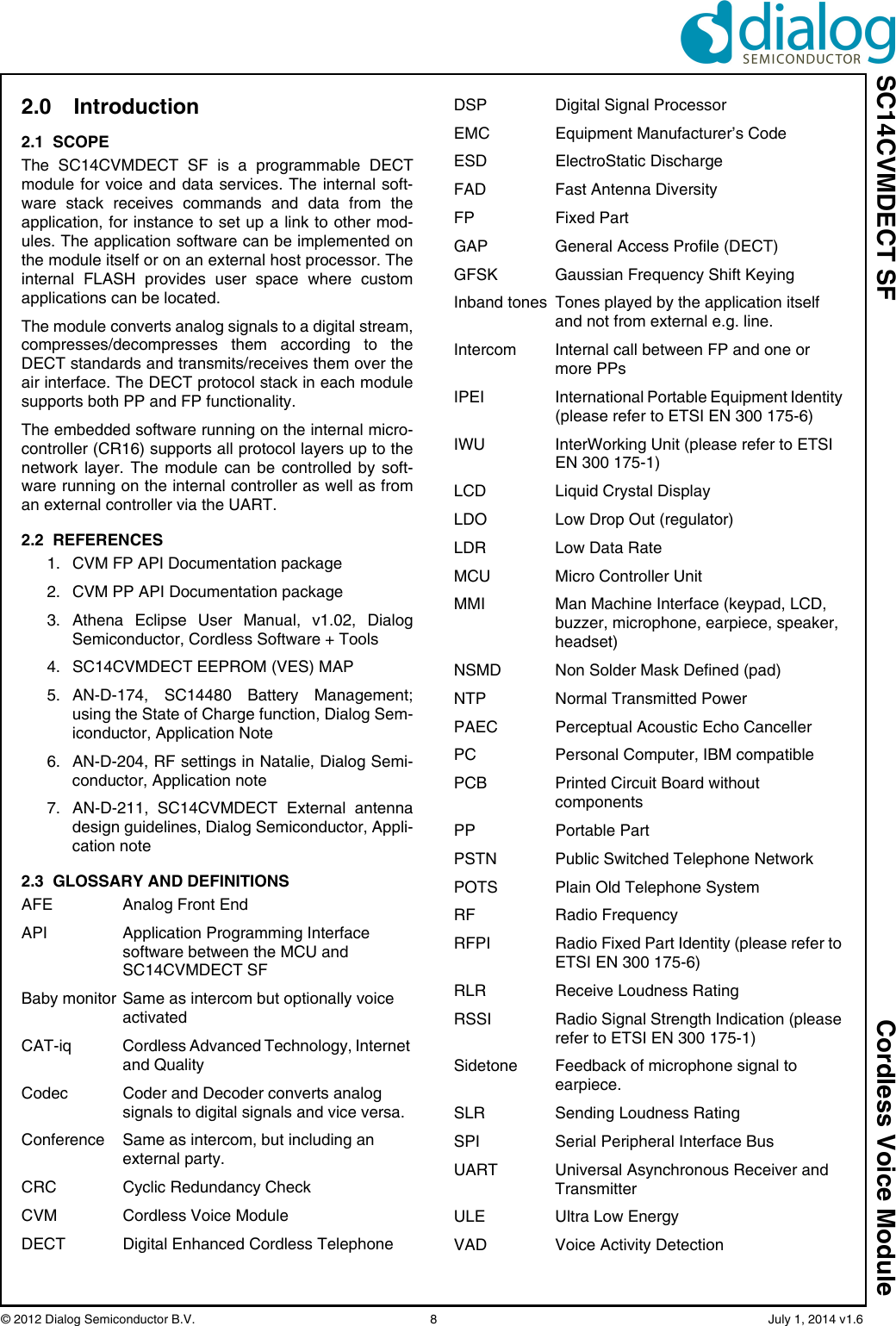
![SC14CVMDECT SF Cordless Voice Module© 2012 Dialog Semiconductor B.V. 10 July 1, 2014 v1.63.0 Cordless Voice Module function-alityThis section describes the key functions and featuressupported by the SC14CVMDECT SF as shown in Fig-ure 2.3.1 MODULE HARDWARE The SC14CVMDECT SF internal hardware consists of:• An internal microprocessor is running from FLASH and handles the API call coming from UART or embedded user software.• A 4 kB VES (Virtual EEPROM Storage) used by the protocol stack and for user variables.• A DSP for the audio signal processing like ADPCM voice compression towards the CODEC.• A CODEC converts the analog signals to digital sig-nals and vise versa.• Input/Output ports which can be toggled high/low as an output or a high/low digital level can be read as an input.• A 20.736 MHz XTAL. This crystal is automatically tuned by the PP module software for optimal radio performance.• Voltage regulators convert the external supply volt-age (VBAT) to stable supply voltages for the core and the I/Os.• A DECT radio transceiver with a built-in antenna cir-cuit. The antenna itself is integrated into the module, relieving the product designer from RF expertise.• A full duplex UART for communication with an optional host processor.3.2 SOFTWARE CONTROLThe application software is written by the customer andhas to manage the call control and also the MMI func-tions. The supported API software includes the Net-work layer that is defined in figure 1 of the EN300 175-3 document, which describes the DECT protocol stack.Detailed functions and data flows, including someexample sequences, can be found in document refer-ence [1] for FP and [2] for PP.3.3 DECT PROTOCOL STACKThe SC14CVMDECT SF internal protocol stack isbased on the ETSI DECT specifications and is compli-ant with ETSI 300 444 (GAP).The product supports up to 6 DECT GAP compliant PPunits to one FP station.Figure 2 SC14CVMDECT SF functional overviewFLASH User SW UART XTALPhoenix Host APICODEC / PCMAPI commandsUART interface to hostSPIPortsPort PinsPCM PortHead SetDECT RFDSPProtocol StackRadio](https://usermanual.wiki/Dialog-Semiconductor/SC14S.user-manual-CVMDECT/User-Guide-2324864-Page-10.png)
![SC14CVMDECT SF Cordless Voice Module© 2012 Dialog Semiconductor B.V. 11 July 1, 2014 v1.63.4 PORTABLE PART CONFIGURATIONA Portable Part configuration with SC14CVMDECT SFrequires additional external parts as shown in Figure 3. .Table 2 provides an overview of the supported inter-faces for a portable part. Note 4: AFE setting is configurable, refer to document [2].3.5 FIXED PART CONFIGURATIONA Fixed Part configuration with SC14CVMDECT SFrequires additional external parts as shown in Figure 4.Figure 3 PP configurationSC14CVMDECTLoudspeakerMIC (handset)Earpiece (handset)MCUHeadsetUARTPorts PCMTable 2: PP support overviewItem Supported RemarkBattery management Yes Supported by APIKeypad No On external MCUDisplay No On external MCUIO Ports Yes All digital IO port pins can be controlled by APIPCM interface Yes 1x 16 bits serial I/O, PCM_FSC 8 kHz/16 kHzUART Yes 115.2 kbit/s, used for API-commandsHeadset detection Yes Supported by APILSR (Earpiece, headset) Yes Connected to LSRp and/or LSRn supports single-end and differential (Note 4)MIC (Earpiece, headset, handsfree)Yes Connected to MICp and/or MICn and/or MIChsupports single-ended and differential (Note 4)Handsfree speaker Yes Connected to PAOUTp/n (Note 4)Radio Yes Integrated single antenna and support for external antenna(s)](https://usermanual.wiki/Dialog-Semiconductor/SC14S.user-manual-CVMDECT/User-Guide-2324864-Page-11.png)
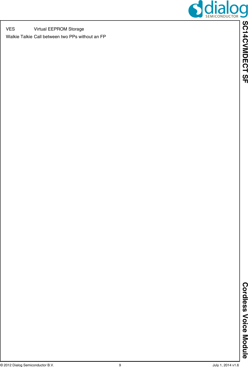
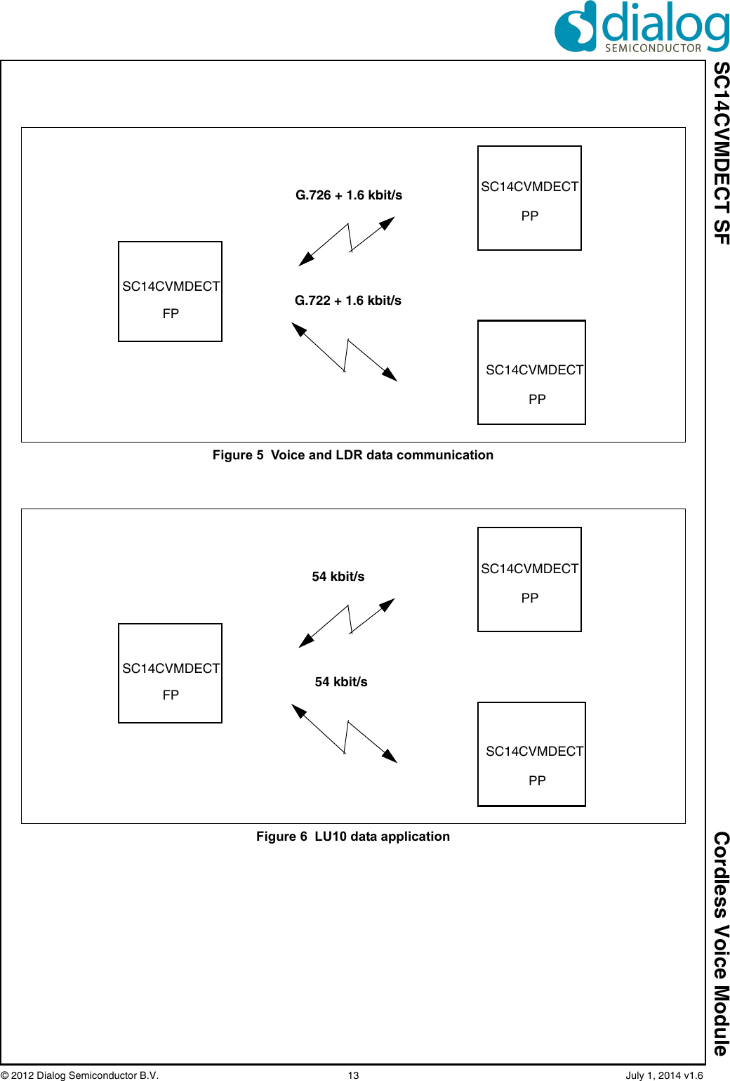
![SC14CVMDECT SF Cordless Voice Module© 2012 Dialog Semiconductor B.V. 12 July 1, 2014 v1.6.Table 3 provides the overview of required and availa-ble interfaces for a basic or a feature rich cordless FPwith the SC14CVMDECT SF. .Note 5: AFE setting is configurable, refer to document [1].3.6 VOICE COMMUNICATIONAn FP supports up to 6 registered PPs, where 4 ofthese PPs can be in a call at the same time. Multiplesimultaneous calls are supported. Supported voicecodec is G.726 (32 kbit/s ADPCM) and G.722 (64 kbit/sADPCM). See Figure 5.3.7 LIGHT DATA APPLICATIONThe SC14CVMDECT SF supports Low Data Rate(LDR) transmission up to 1.6 kbit/s with IWU to IWUmessaging. The LDR can be used in combination withvoice communication. See Figure 5.3.8 LU10 DATA APPLICATIONThe SC14CVMDECT SF supports CAT-iq LU10 datatransmission up to 54 kbit/s. Since LU10 data commu-nication uses the B-Field it cannot be used in combina-tion with voice communication. See Figure 6. Figure 4 FP configurationSC14CVMDECTLoudspeakerMIC (handset)Earpiece (handset)MCUSupplyPortsHeadsetRegulatorPCMUARTTable 3: FP support overviewItem Supported RemarkSupply Regulator No Use external 3.3 V LDOKeypad No On external MCUDisplay No On external MCUIO Ports Yes All digital IO port pins can be controlled via APIPCM interface Yes 4x 16 bits serial I/O, PCM_FSC 8 kHz/16 kHzUART Yes 115.2 kbit/s, used for API-commandsHeadset detection No Not supported by APILSR (Earpiece, headset) Yes Connected to LSRp and/or LSRn supports single-end and differential (Note 5)MIC (Earpiece, headset, handsfree) Yes Connected to MICp and/or MICn and/or MIChsupports single-end and differential (Note 5)Handsfree speaker Yes Connected to PAOUTp/n (Note 5)PSTN Line interface No Not supported by APIRadio Yes Integrated single antenna and support for external antenna(s)](https://usermanual.wiki/Dialog-Semiconductor/SC14S.user-manual-CVMDECT/User-Guide-2324864-Page-12.png)
![SC14CVMDECT SF Cordless Voice Module© 2012 Dialog Semiconductor B.V. 14 July 1, 2014 v1.63.9 GENERAL FEATURESStandard FP audio control feature.Note 6: These features can be supported by combined API commands in user software.Table 4: Supported general featuresFunctionality (Note 6) PP supportFP support RemarkCall handlingConferencing - Yes Call between FP and 4x PPIntercom Yes Yes Call between FP and 4x PPWalkie Talkie mode Yes - Call between PP and PP without FPBaby monitor Yes - Voice Activated PP. See document reference [2]Voice over PCM interface Yes Yes -law (64 kbit/s), A-law (64 kbit/s), G.726 ADPCM (32 kbit/s), G.722 ADPCM (64 kbit/s), Linear (128 kbit/s)Call transfer Yes Yes Transfer call between PPs on FPPage call Yes Yes FP pages all PPs (PP locator)ProtocolManual registration Yes YesNumber of registered PPs per FP Yes - 1 to 6 Audio and toneMicrophone mute Yes YesTone generation Yes No Melody generator with 7 polyphonic tonesAudio Volume control Yes YesTone Volume control Yes NoHeadset support Yes YesHandsfree/Speakerphone Yes NoGeneralReal time clock Yes Yes Accuracy depending directly on crystalReal time clock synchronization Yes Yes All PP clocks are kept in synchronization with the FPSW EEPROM (VES) Storage Yes Yes Internal on moduleBattery Charge Management Yes NoPSTN line interface support - No PSTN software on requestI/O port support Yes YesPort Interrupt support No NoAutomatic headset detection Yes NoLow speed data Yes Yes 1.6 kbit/sLU10 data channel Yes Yes 54 kbit/sCAT-iq up to version 2.0, 3.0 Yes YesULE applications - Yes Number of ULE subscriptions: up to 180.](https://usermanual.wiki/Dialog-Semiconductor/SC14S.user-manual-CVMDECT/User-Guide-2324864-Page-14.png)
![SC14CVMDECT SF Cordless Voice Module© 2012 Dialog Semiconductor B.V. 15 July 1, 2014 v1.64.0 Functional description4.1 UART INTERFACEThe UART is normally used for API commands, butcan also be used for software upgrades and debug-ging. The UART is a full duplex UART with frame type: 1 start bit,8 data bits (LSB first),1 stop bit,no parity,up to 115.2 kBd.The UART hardware interface uses only TX/RX(see Figure 7). Caution: All signals are 1.8 V (see Table 8, Table 9and Table 10). An external V.24 line driver must beprovided if the UART port of the module is connectedto a standard V.24 device. Connecting the modulewithout a driver may damage the module.4.2 VES (VIRTUAL EEPROM Storage)4.2.1 VES layoutThe SC14CVMDECT SF PP and FP include a 4 kBVES which is divided into two areas (see Table 5).VES is supported as virtual EEPROM with the internalFLASH.A detailed overview of the VES parameters can befound in document reference [4].Some parts of the VES parameters are read into theSC14CVMDECT SF during the start up and other partsare used by the SC14CVMDECT SF software duringexecution. The VES parameters are divided into 2 types:• Factory type • Normal type The factory type is specific for the SC14CVMDECT SFand should only be set by production. The factory typeparameters are either adjustments used by the base-band or the radio interface, or are used to set up theSC14CVMDECT SF into special modes. The factorytype parameters will only be modified by changing thefactory programmed default value. See document ref-erence [4]. The “normal” VES parameters can be reset to theirdefault values via software.4.2.2 VES access by MCUThe host is able to read or modify the VES parametersor limited free VES areas via API command. 4.3 AUDIO CONFIGURATIONSThe SC14CVMDECT SF audio supports standardDECT audio qualities. The audio gain and volumeparameters are placed in the VES. The DECT gainscan be adjusted to meet the TBR38 and TBR10 audiolevel requirements by using the SC14CVMDECT SFapplication reference design. For other line and acous-tic designs it is required to adjust and tune the audiosetup.Figure 7 UART hardware configurationSC14CVMDECT MCUTX (serial out), module pin 48RX (serial in), module pin 47GNDTable 5: VES mapVES space Size UsageSC14CVMDECT SF3.6 kB Used for RF, audio, battery, tone setup, data base, etc.User 0.4 kB Can be used for MMI applications such as User infor-mation.](https://usermanual.wiki/Dialog-Semiconductor/SC14S.user-manual-CVMDECT/User-Guide-2324864-Page-15.png)
![SC14CVMDECT SF Cordless Voice Module© 2012 Dialog Semiconductor B.V. 17 July 1, 2014 v1.64.4 AUDIO ROUTING4.4.1 FP AUDIO ROUTINGFigure 10 shows the audio routing for a FP. Input andoutput signals are supported both for the internal codecand the PCM, and the Air interface supports G.726(32 kbit/s ADPCM) and G.722 (64 kbit/s ADPCM). Theinternal software supports up to 4 audio channelssimultaneously. Supported sample rates are 8 kHz and16 kHz.FP does not support acoustic or line echo cancellation.4.4.2 FP audio level adjustmentThe internal codec audio levels can be controlled withthe parameters MicGain and LsrGain.The MicGain range is 0 to 30 dB in steps of 2 dB and avalue of -128 will mute the input signal, default is 0 dB.The LsrGain range is +2 dB to -12 dB in steps of 2 dB,default is +2 dB. See document reference[1].4.4.3 PP audio routingFigure 11 and Figure 12 show the different audio rout-ing modes of a PP. Figure 11 shows an overall audiorouting and Figure 12 shows the detailed audio routingfor the speakerphone of PP (FP does not supportspeakerphone).4.4.4 PP audio codec adjustmentThe audio codec settings for the loudspeaker andmicrophone must be pre-configured in the VES foreach mode. The VES parameter fields forAudio.Earp.xxxAudio.Heads.xxxAudio.SpkPh.xxxhave a default value and maybe fine-tuned for theapplication. See document reference[4].4.4.5 General audio adjustmentFor each audio mode, the receive (RLR) and transmit(SLR) audio paths must be adjusted. RLR and SLR areadjusted in the registers in the VES for each audiostate; see document reference [4]. Figure 13 showsthis image.4.4.6 PP volumeThe PP supports 6 volume steps, which are VES con-figurable through parameter fields Audio.Earp.Vol.xxx,the Audio.Heads.Vol.xxx and Audio.SpkPh.Vol.xxx.The volume steps must be set initially in the VES dur-ing production; see document reference [4].4.4.7 PP audio equalizationTo enable adjustments of the frequency response thePP contains four programmable filters: 2 in RX direc-tion and 2 in TX direction (see Figure 11).By default these filters are loaded with bypass coeffi-cients. These can be modified by loading new coeffi-cients via API commands.Equalizer filters are part of the audio routes for allaudio modes and are placed as shown in Figure 11.For a detailed description of the filter functionality referto the API documentation; see document reference [2].Figure 10 FP audio routingMask &ShiftG726EncoderG726EncoderG726EncoderG726EncoderMacRxG726EncoderG726EncoderG726EncoderG726DecoderMacTxG726EncoderG726EncoderG726EncoderG722EncoderMacRxG726EncoderG726EncoderG726EncoderG722DecoderMacTxMacUnitSoft Mute(bit errors on air interface)IoCtrlIoCtrlIoCtrlIoCtrlPCMxInCodecInPCMxOutCodecOutMask &ShiftMask &ShiftMask &Shift G711DecoderG711DecoderG711DecoderG711DecoderCWBUnpackCWBUnpackCWBUnpackCWBUnpackIoCtrlIoCtrlIoCtrlIoCtrlMask &ShiftMask &ShiftMask &ShiftMask &Shift G711DecoderG711DecoderG711DecoderG711EncoderCWBUnpackCWBUnpackCWBUnpackCWBPack](https://usermanual.wiki/Dialog-Semiconductor/SC14S.user-manual-CVMDECT/User-Guide-2324864-Page-17.png)
![SC14CVMDECT SF Cordless Voice Module© 2012 Dialog Semiconductor B.V. 19 July 1, 2014 v1.64.5 PP AUDIO MODESThe PP audio handling consists of four audio states(see Figure 14). In these states the audio subsystem isconfigured for a certain audio mode:1. Idle mode (not relevant for microphone configu-ration)2. Earpiece mode (Handset speaker)3. Handsfree or Speakerphone mode4. Headset modeSelection between the modes is done via API calls; seedocument reference [2].The Alert state is for tone playing and is entered auto-matically when tones are played using the API calls.The Alert state can originate from idle, earpiece,handsfree or headset mode. 4.5.1 Power managementTo minimize the current consumption the PP will shutdown all codec amplifiers in Idle mode. This meansthat all reference voltages in the analog front-end willbe disabled. This feature can be disabled in the VES ifthe reference voltages for some reasons are needed inIdle mode.Figure 13 Handset volume configurationFigure 14 PP audio modesIdleEarpiece AudioHandsfree Audio API_PP_ AUDIO_SET_ MODE_ REQ(API_ AUDIO_ MODE_ EARPIECE ) API_PP_ AUDIO_SET_ MODE_ REQ(API_ AUDIO_ MODE_ EARPIECE ) API_PP_ AUDIO_SET_ MODE_ REQ(API_ AUDIO_ MODE_ HANDSFREE )Headset Audio API_PP_ AUDIO_SET_ MODE_ REQ(API_ AUDIO_ MODE_ HEADSET ) API_PP_ AUDIO_ SET_ MODE_ REQ(API_ AUDIO_ MODE_ EARPIECE ) API_PP_ AUDIO_SET_ MODE_REQ(API_ AUDIO_ MODE_ HEADSET) API_PP_ AUDIO_ SET_ MODE_ REQ( API_ AUDIO_ MODE_ EARPIECE )](https://usermanual.wiki/Dialog-Semiconductor/SC14S.user-manual-CVMDECT/User-Guide-2324864-Page-19.png)
![SC14CVMDECT SF Cordless Voice Module© 2012 Dialog Semiconductor B.V. 21 July 1, 2014 v1.6SC14CVMDECT SF crystal. When the SC14CVMDECT SF is configured as a PP,the clock has the same accuracy as the FP clock.When the PP synchronises with a FP, the PP crystal issynchronized with the FP crystal and the PP clock willchange accordingly.The accuracy is expected to be within 1 minute for upto 6 weeks without being locked to a FP. 4.9 BATTERY MANAGEMENTFigure 18 shows a handset application with NiMH.SOC (State Of Charge) is used to measure the amountof charge in the rechargeable batteries.Figure 19 shows an FP application. The FP uses anexternal LDO, so the SOC pins are not used and canbe connected to GND.The PP API supports battery management to calculatethe battery capacity and to indicate charge status.Refer to API document [2].The SOC circuit is used to very accurately determinethe amount of charge in rechargeable batteries as wellas the discharge state of Alkaline batteries. This infor-mation is essential for the battery charging algorithmand necessary for battery status indication to the user.Battery status information is supported by the API.Detailed information can be found in AN-D-174 (Bat-tery Management).Pin CHARGE_CTRL is driven high when either the“sensed voltage on the VBAT pin” is lower than thevoltage setting or “sensed current via SOCp” is lowerthan the current setting. Pin CHARGE_CTRL can driveup to 500 A as source current (see Table 20).Detailed setting information can be found in document[4] under “Battery settings”.4.10 PROTOCOL STACKThe protocol stack handles the RF interface, the MAC-,DLC-, NWK-layer and encryption according to theDECT standard EN300 175 1-9.4.10.1 DECT TBR22The SC14CVMDECT SF supports the DECT GAPstandard according to EN300 444. For TBR22 typeapproval (optional) switching off the authentication andencryption is required, which can be done with the VESparameter Tbr_22.Figure 17 Clock synchronizationFigure 18 Handset (PP) application with 2x NiMH100CHARGE_CTRL1k1k0.1SOCCHARGESOCpSOCnVsupply VBAT INFigure 19 Base station (FP) applicationCHARGE_CTRL1kSOCCHARGESOCpSOCnVsupply VBAT INLDO](https://usermanual.wiki/Dialog-Semiconductor/SC14S.user-manual-CVMDECT/User-Guide-2324864-Page-21.png)
![SC14CVMDECT SF Cordless Voice Module© 2012 Dialog Semiconductor B.V. 22 July 1, 2014 v1.64.10.2 Out-of-Range handlingWhen the PP goes in-range or out-of-range a signal issent from the PP to the MMI software indicatingwhether the PP is in-lock or is out-of-lock with the FP.4.10.3 Preamble antenna diversityTo optimise the audio quality caused by rapidly chang-ing radio paths (fading), the SC14CVMDECT SF sup-ports preamble antenna diversity. The preamblediversity algorithm uses RSSI measurements to judgethe radio signal strength on both antennas and, as aresult, the choice of the best performing antenna isdetermined. This antenna will then be used for thereceive slot and the next transmit slot.The preamble antenna diversity is supported with twoantennas. The preamble diversity can be controlled byVES. See document reference [4] and Section 4.13 formore information about antenna diversity.4.10.4 Broadcasting messagesMessages consisting of up to 19 bytes can be broad-casted from FP to all registered PPs. Broadcastingdoes not require an active connection. Broadcastingdoes not use retransmission, therefore broadcasting isnot secured. If the real time clock is enabled this data isalso broadcasted to all PPs.4.10.5 IWU to IWU messaging The protocol in the SC14CVMDECT SF module ismade according to the DECT/GAP standard as definedin EN 300 175 and EN 300 444.The DECT standard defines an EMC code (seeEN 300 175-5, chapter 7.7.23.). This code is unique fora DECT product and must be programmed by theDECT manufacturer to the correct manufacturer code. The EMC code must be the same for SC14CVMDECTSF based product families when using the IWU to IWUmessaging.If the Dialog default EMC VES value is changed theIWU to IWU messaging may not operate correctly.IWU data is transferred in a FA format frame; seechapter 6.1 in EN 300 175-4. This frame has an infor-mation field of maximum 63 bytes of which maximum52 bytes can be used for IWU data. With theSC14CVMDECT SF it is only possible to send5 frames in a row without pause. The following framemust be an acknowledge-frame to secure that theinternal buffers within the SC14CVMDECT SF areemptied.The FA frame is segmented in 5 byte fragments andtransferred over the air-interface in the A-field. The 2-bytes CRC is used to determine if the data is receivedcorrectly. If the data is not received correctly this is sig-nalled back to the transmitter by the Q2 bit, and thedata is retransmitted.The FA frame has a 2 bytes checksum, used to deter-mine if the complete packet is received correctly. If Achecksum error is signalled back to the transmitter andthe complete packet is retransmitted. The packet willbe retransmitted until it is received correctly, or until thelink is closed.More transmitted packets will be received in the sameorder as they were transmitted. The application musthandle flow control, if needed.4.11 REGISTRATIONThe PP and the FP must be paired using a procedurecalled Registration. Without Registration, the PP will beout-of-lock and will not be able to establish a link to aFP and therefore not be able to make a call. The regis-tration uses the unique product identities and securesthe PP and FP to allow no cross-communication.The PP can be de-registered from a FP either via theFP or PP MMI Software using the command interface.It is also possible to deregister a PP from another reg-istered PP.It is possible to pair a PP and FP during the production. 4.11.1 Handling product identitiesTo secure that the FP and PPs do not make cross-communications a unique ID must be entered into theVES of an FP or PP. For the DECT version the ID forthe FP is named RFPI and for the PP the ID is namedIPEI. These numbers are factory settings. After a successful registration, the IPEI is stored in theFP and the RFPI is stored in the PP. In this way the twoparts are known to each other and are allowed to makeconnections. The registration data are automaticallystored in VES of the FP and PP while making the regis-tration.It is possible to register the same PP to 2 FPs, but itcan only be used in one FP at the same time.](https://usermanual.wiki/Dialog-Semiconductor/SC14S.user-manual-CVMDECT/User-Guide-2324864-Page-22.png)
![SC14CVMDECT SF Cordless Voice Module© 2012 Dialog Semiconductor B.V. 23 July 1, 2014 v1.64.11.2 DeregistrationThere are two ways of deregistering a PP from an FP:• Remote FP and PP deregistrationThe correct way to deregister a PP from an FP is to deregister it remotely in the FP. If this is done over a service connection from the PP to the FP, the FP actually performs the deregistration and then it is automatically signalled to the PP which in turn will drop out-of-lock. Using this method it is also possible to deregister other PPs registered to the FP from one PP.• Removing all registrations at once from the FP (e.g. in case the original PPs are lost).4.12 PCM INTERFACEThe PCM supports the following modes:• SLAVE mode clock sync. In this mode the clock of the module will be adjusted to follow the PCM pro-vided by the external PCM master clock. All audio samples are kept if the provided PCM clock accu-racy is +/- 5 ppm, which is a DECT radio require-ment.• SLAVE no clock sync. In this mode the clock of the module is not synchronized. This means audio sam-ple will be discarded in case the master PCM clock is faster than the clock of the module or samples will be repeated in case the master PCM clock is slower.• MASTER mode. The FP is master on PCM interface and therefore provides PCM clock and PCM_FSC to an external device.4.12.1 PCM Interface for FPThe SC14CVMDECT SF supports PCM interface func-tionality to connect to an external audio source/destina-tion.The different PCM interface modes and timings areshown in Figure 21 to 26. Refer to document [1] fordetailed information.4.12.2 PCM_FSC frequencyThe PCM interface supports the following options:• 8 kHz• 16 kHz4.12.3 Length of PCM_FSCThe PCM interface supports the following options:• 1: The length of PCM_FSC pulse is equal to1 data bit.• 8: The length of PCM_FSC pulse is equal to8 data bits.• 16: The length of PCM_FSC pulse is equal to16 data bits.• 32: The length of PCM_FSC pulse is equal to32 data bits.4.12.4 Start position of FSCThe PCM interface supports the following options:• The FSC pulse starts 1 data bit before the MSB bit of the PCM channel 0 data.• The FSC pulse starts at the same time as the MSB bit of the PCM channel 0 data.4.12.5 PCM clock frequencyThe PCM interface supports the following options inmaster mode:• 1.152 MHz• 2.304 MHzFigure 20 Handling product identities](https://usermanual.wiki/Dialog-Semiconductor/SC14S.user-manual-CVMDECT/User-Guide-2324864-Page-23.png)
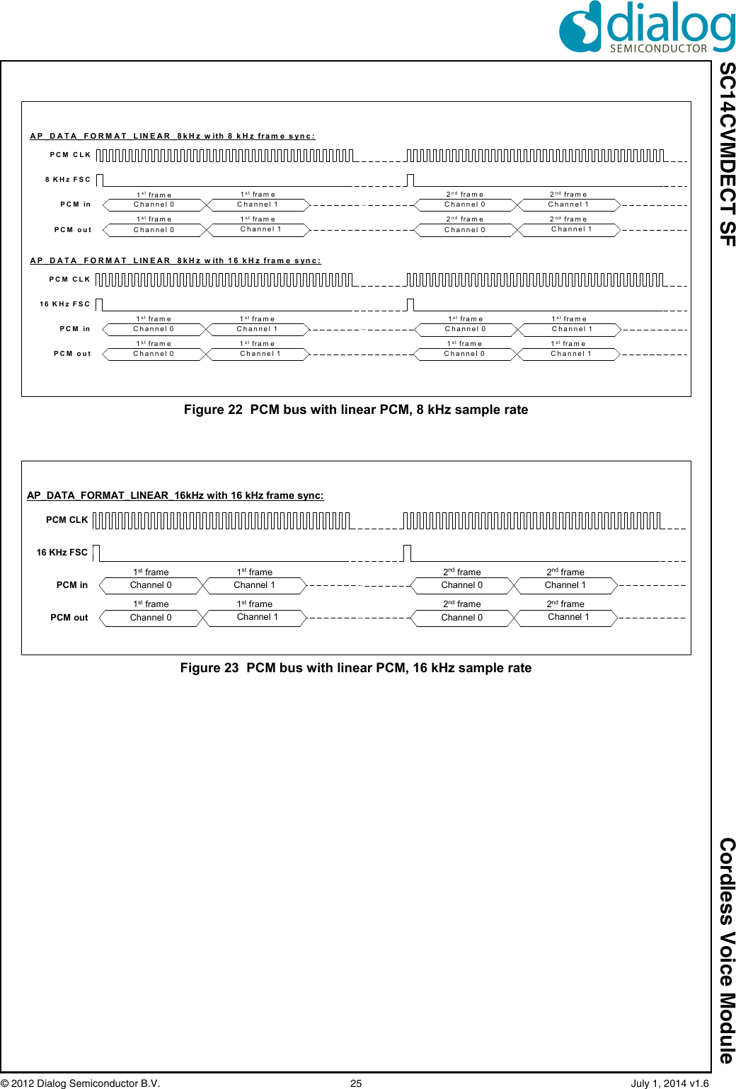
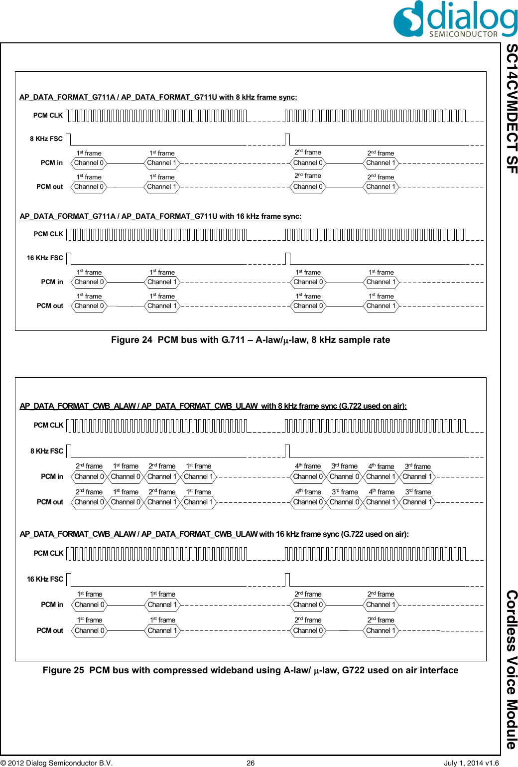
![SC14CVMDECT SF Cordless Voice Module© 2012 Dialog Semiconductor B.V. 24 July 1, 2014 v1.6• 4.608 MHz• 1.536 MHz4.12.6 PCM data modeThe PCM interface supports the following PCM dataformats: • Linear PCM, 8 kHz sample rate. Used for narrowband calls (G.726).• Linear PCM, 16 kHz sample rate. Used for wideband calls (G.722).• G.711 – A-law, 8 kHz sample rate. Used for narrowband calls (G.726).• G.711 – -law, 8 kHz sample rate. Used for narrowband calls (G.726).• Compressed wideband using A-law, 16 kHz sample rate. The 16 bit PCM data is encoded as two 8 bit audio samples if 8 kHz frame sync is used. Used for wideband calls (G.722).• Compressed wideband using -law, 16 kHz sample rate. The 16 bit PCM data is encoded as two 8 bit audio samples if 8 kHz frame sync is used. Used for wideband calls (G.722).Figure 21 PCM interface formatsChannel 3Channel 3Channel 2Channel 2Channel 1Channel 1Channel 0Channel 0DSP_PCM_CTRL_REG[5,4,3] = 000DSP_PCM_CTRL_REG[5,4,3] = 010DSP_PCM_CTRL_REG[5,4,3] = 100DSP_PCM_CTRL_REG[5,4,3] = 101DSP_PCM_CTRL_REG[5,4,3] = 111DSP_PCM_CTRL_REG[5]=0DSP_PCM_CTRL_REG[5]=1PCM Slave modeD15 D8 D7 D0PCM MasterDSP_PCM_CTRL_REG[5,4,3] = 001DSP_PCM_CTRL_REG[5,4,3] = 011DSP_PCM_CTRL_REG[5,4,3] = 110PCM_CLK PCM_CLKPCM_DI PCM_DOPCM_FSC (input) PCM_FSC (input) PCM_FSC PCM_FSC PCM_FSC PCM_FSC PCM_FSC PCM_FSC PCM_FSC PCM_FSC](https://usermanual.wiki/Dialog-Semiconductor/SC14S.user-manual-CVMDECT/User-Guide-2324864-Page-24.png)
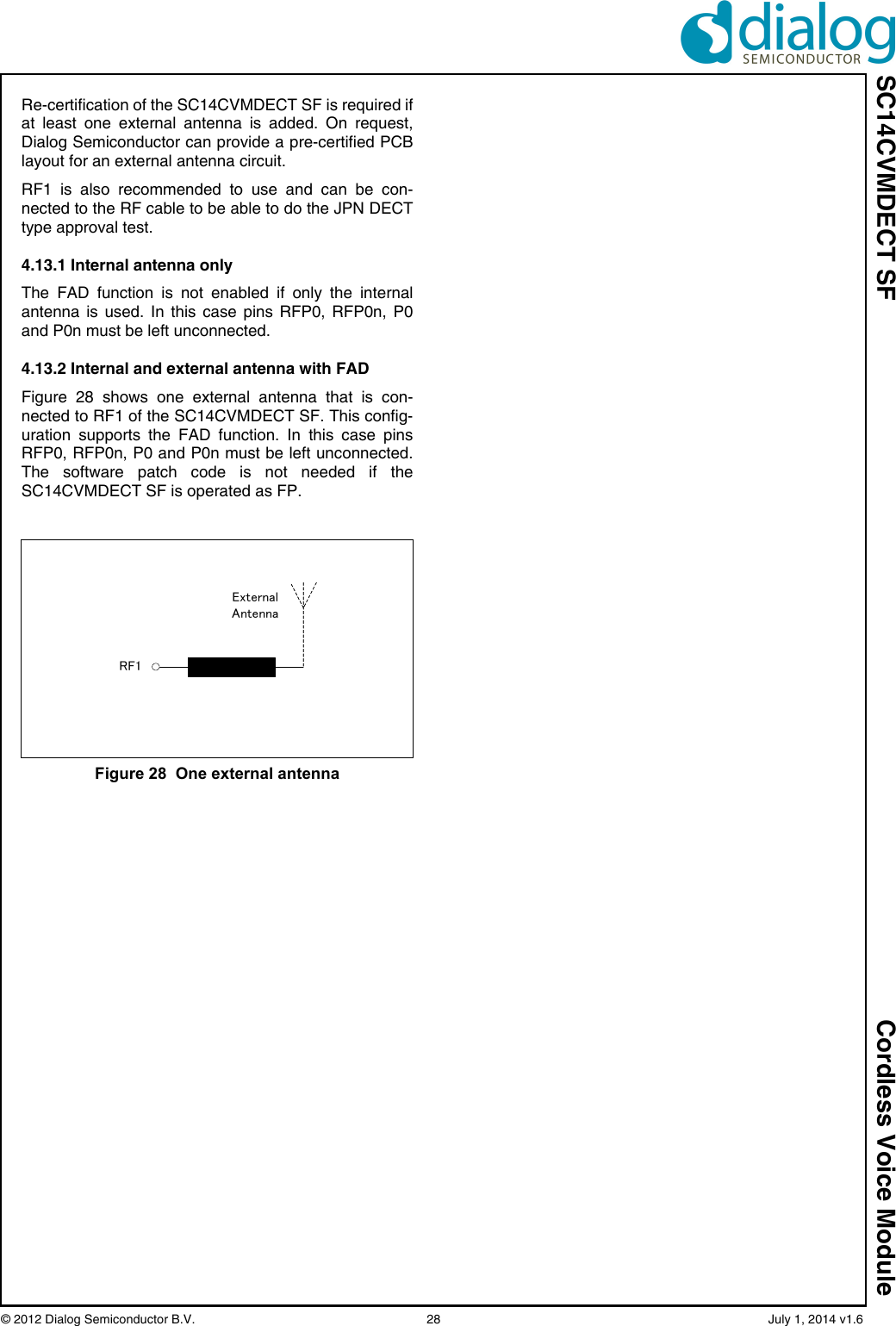
![SC14CVMDECT SF Cordless Voice Module© 2012 Dialog Semiconductor B.V. 27 July 1, 2014 v1.64.12.7 PCM Interface for PPThe SC14CVMDECT SF supports PCM interface func-tionality to connect to an external audio source/destina-tion. Refer to document [2] for detailed information.• PCM interface modesupports only master mode.• PCM_FSC frequency supports 8 kHz and 16 kHz.• LENGTH of PCM_FSCThe PCM interface supports the following options:• 1: The length of PCM_FSC pulse is equal to 1 data bit.• 8: The length of PCM_FSC pulse is equal to 8 data bits.• 16: The length of PCM_FSC pulse is equal to 16 data bits.• 32: The length of PCM_FSC pulse is equal to 32 data bits.• Start position of FSCThe PCM interface supports the following options:• The FSC pulse starts 1 data bit before MSB bit of the PCM channel 0 data.• The FSC pulse starts at the same time as the MSB bit of the PCM channel 0 data.• PCM clockPCM clock is delivered to an external slave PCM device from SC14CVMDECT SF.• PCM Data modeSupports only linear 16 bit PCM.4.13 ANTENNA OPERATIONFigure 27 shows the internal circuit of theSC14CVMDECT SF. Pin RF0 is used for two externalantennas and can also be used for RF test purposes,so it is recommended to add a 10 pF capacitor asreserve pattern even when the two external antennasare not used.Figure 26 PCM bus with compressed wideband using A-law/ -law, G726 used on air interfacePCM CLK16 KHz FSCPCM inPCM outChannel 0Channel 0Channel 1Channel 1Channel 0Channel 0Channel 1Channel 1AP_DATA_FORMAT_CWB_ALAW / AP_DATA_FORMAT_CWB_ULAW with 16 kHz frame sync (G.726 on air):1st frame1st frame1st frame1st framePCM CLK8 KHz FSCPCM inPCM outChannel 0Channel 0Channel 1Channel 1Channel 0Channel 0Channel 1Channel 1Channel 0Channel 0Channel 1Channel 1Channel 0Channel 0Channel 1Channel 1AP_DATA_FORMAT_CWB_ALAW / AP_DATA_FORMAT_CWB_ULAW with 8 kHz frame sync (G.726 on air):1st frame1st frame2nd frame2nd frame1st frame1st frame2nd frame2nd frame2nd frame2nd frame2nd frame2nd frame1st frame1st frame1st frame1st frame1st frame1st frame1st frame1st frameFigure 27 Internal circuit of the SC14CVMDECT SFRF1TP1Internal antennaRF0P0nP0TXRXRFP0nRFP0](https://usermanual.wiki/Dialog-Semiconductor/SC14S.user-manual-CVMDECT/User-Guide-2324864-Page-27.png)
![SC14CVMDECT SF Cordless Voice Module© 2012 Dialog Semiconductor B.V. 32 July 1, 2014 v1.66.5 ANALOG FRONT ENDNote 14: BANDGAP_REG will be tuned at the factory.Note 15: 0 dBm0 on COUT = -3.14 dB of max PCM value. COUT is CODEC output in test modeNote 16: Trimming possibility is foreseen. At system production the bandgap reference voltage can be controlled within 2% accuracy and data can be stored in Flash. Either AVD or VREF can be trimmed within 2% accuracy. If AVD is trimmed VREF will be within 2% accuracy related to either AVD. Or vice versa VREF can be trimmed. For Vref trimming measure VREFp, VREFm) and update BANDGAP_REG[3..0].Note 17: Vrefm is a clean ground input and is the 0 V reference.Table 11: Microphone amplifierPARAMETER DESCRIPTION CONDITIONS MIN TYP MAX UNITVmic_0dB_unt Untrimmed differen-tial RMS input volt-age between MICp and MICn (0 dBm0 reference level) (Note 7)0 dBm0 on COUT(Note 15)MIC_GAIN[3:0] = 0, @ 1020 Hz;Tolerance:• 13% when untrimmed (BANDGAP_REG=8) (Note 14)• 6% when trimmed (Note 16)114 131 149 mVRin_mic Resistance of acti-vated microphone amplifier inputs (MICp, MICn and MICh) to internal GND (Note 7)75 150 kVmic_offset Input referred DC-off-set (Note 7)MIC_GAIN[3..0] = 11113 sigma deviation limits-2.6 +2.6 mVTable 12: Microphone amplifier (Operating Condition)PARAMETER DESCRIPTION CONDITIONS MIN TYP MAX UNITVmic_cm_level MICp and MICn com-mon mode voltageMICp and MICn are set to GND with internal resistors (Rin_mic). If DC coupled the input voltage must be equal to this voltage.(0.9 V/1.5)* VREFp VTable 13: Microphone supply voltagesPARAMETER DESCRIPTION CONDITIONS MIN TYP MAX UNITVref_unt VREFp-VREFm untrimmed (Note 17)ILOAD = 0 mA BANDGAP_REG = 8 (Note 16)1.41 1.5 1.59 VRout_vrefp VREFp output resistanceFigure 29 1Nvrefp_idle Peak noise on VREFp-VREFm(Note 7)CCITT weighted -120 dBVPSRRvrefp Power supply rejec-tion Vref output (Note 7)See Figure 29, AVD toVREFp/m, f = 100 Hz to 4 kHzBANDGAP_REG[5:4] = 340 dB](https://usermanual.wiki/Dialog-Semiconductor/SC14S.user-manual-CVMDECT/User-Guide-2324864-Page-32.png)
![SC14CVMDECT SF Cordless Voice Module© 2012 Dialog Semiconductor B.V. 33 July 1, 2014 v1.6Note 18: 0 dBm0 on CIN = -3.14 dB of max PCM value.Table 14: VREFp load circuitPARAMETER DESCRIPTION CONDITIONS MIN TYP MAX UNITCload_vrefp VREFp (parasitic) load capacitance20 pFIout_vrefp VREFp output current 1mAFigure 29 VREFp load circuitCload_vrefpVREFpVREFmIout_vrefpRout_vrefpTable 15: LSRp/LSRn outputsPARAMETER DESCRIPTION CONDITIONS MIN TYP MAX UNITVlsr_0dB_unt Untrimmed differen-tial RMS output volt-age between LSRp and LSRn in audio mode (0 dBm0 refer-ence level)0 dBm0 on CIN (Note 18), LSRATT[2:0] = 001, @ 1020 Hz Load circuit A (see Figure 30, Table 16) with RL1= , Cp1 or load circuit B (see Figure 31) with RL2, Cp2 and Cs2Tolerance:• 13% when untrimmed (BANDGAP_REG=8)• 6% when trimmed (Note 16)621 714 807 mVRout_lsr Resistance of acti-vated loudspeaker amplifier outputs LSRp and LSRn1Vlsr_dc DC offset between LSRp and LSRn (Note 7)LSRATT[2:0] = 3RL1 = 28 3 sigma deviation limits-20 20 mV](https://usermanual.wiki/Dialog-Semiconductor/SC14S.user-manual-CVMDECT/User-Guide-2324864-Page-33.png)
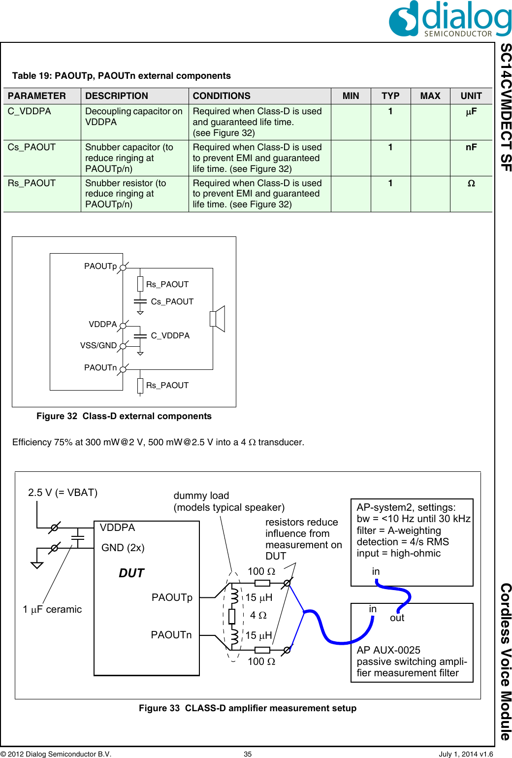
![SC14CVMDECT SF Cordless Voice Module© 2012 Dialog Semiconductor B.V. 34 July 1, 2014 v1.6Note 19: Clipping of the outputs occurs when the VDDPA drops and the following conditions becomes true. If CLASSD_CTRL_REG[CLASSD_CLIP] is not equal to zero then upon a programmable number of clipping occurrences a CLASSD_INT is generated:The software can stop clipping by reducing the gain via the GENDSP:Clipping occurs ifTable 16: LSRp/LSRn load circuitsPARAMETER DESCRIPTION CONDITIONS MIN TYP MAX UNITCp1_Rl1_inf Load capacitance see Figure 30, RL1 = 30 pFCp1_Rl1_1k Load capacitance see Figure 30, RL1 1 k100 pFRl1 Load resistance 28 Cp2 Parallel load capacitancesee Figure 31 30 pFCs2 Serial load capacitance 30 FRl2 Load resistance 600 Figure 30 Load circuit A: Dynamic loudspeakerRL1 Cp1LSRpLSRnFigure 31 Load circuit B: Piezo loudspeakerCs2LSRpLSRnRL2Cp2Table 17: PAOUTp, PAOUTn outputsPARAMETER DESCRIPTION CONDITIONS MIN TYP MAX UNITVpa_4v Differential rms output voltage between PAOUTp and PAOUTnTrimmed bandgapinput = 0 dBm0, 1 kHz (Note 15)Output low-pass filteredCLASSD_VOUT = 00.985 VrmsVpa_6v As aboveCLASSD_VOUT = 11.478 VrmsZload_pa_4v Speaker impedance, connected between PAOUTp and PAOUTnWith these values, the peak cur-rents stays within the operating range.4Zload_pa_6v 6Table 18: PAOUTp, PAOUTn outputs (Note 19)PARAMETER DESCRIPTION CONDITIONS MIN TYP MAX UNITRout_pa Differential output resistance between PAOUTp and PAOUTnSee (Note 19) 1peak LowPassFiltered PAOUTp PAOUTm–VDDPA VSSPA–-----------------------------------------------------------------------------------------------------------------------ZloadZload Rout_pa+-------------------------------------------](https://usermanual.wiki/Dialog-Semiconductor/SC14S.user-manual-CVMDECT/User-Guide-2324864-Page-34.png)
![SC14CVMDECT SF Cordless Voice Module© 2012 Dialog Semiconductor B.V. 37 July 1, 2014 v1.66.8 RADIO (RF) PARTStandards compliancy: ETS 301 406 (former TBR6).Table 23: Radio specificationsPARAMETER DESCRIPTION CONDITIONS MIN TYP MAX UNITP_Rx Receiver sensitivity BER = 0.001; TA = 25 °C -93 -92 -89 dBmP_Rx_T Receiver sensitivity, full temperature rangeBER = 0.001; -40 °C TA 85 °C -87 dBmIPL Intermodulation perform-ance level (EN 301 406 section 4.5.7.6)TA = 25 °C; Pw = -80 dBm; f = 2 channels-35 dBmNTP Normal transmitted power DECT: 250 mW 24 26 dBmJ-DECT: 10 mW average per frame for each slot23 24.5 dBmDECT6.0: 100 mW (max peak)20.0 dBmdPrfpa_T RFPA power variation, full temperature range-40 °C TA +85 °C 2.5 4dBFbit Bit rate GFSK modulation 1.152 Mbit/sBW_Tx Transmitter bandwidth DECT GFSK; NTP = 20 dB1.728 MHzTable 24: RFPA preferred settings for various power modes (PP application)Address (VES) Register / Parameter HPM/U(USA)HPM(Europe)HPM/J(Japan)0x3D RF_BBADC_CTRL_REG 0x0380 0x03A0 0x03980x39 RF_PA_CTRL1_REG 0x09A0 0x0CF0 0x2CE00x3B RF_TEST_MODE2_REG 0x0056 0x0062 0x00680x05 RF_PLL_CTRL2_REG[MODINDEX] 0x25 0x25 0x230x23 Upper RSSI threshold 0x2C N/A 0x280x24 Lower RSSI threshold 0x22 N/A 0x1E](https://usermanual.wiki/Dialog-Semiconductor/SC14S.user-manual-CVMDECT/User-Guide-2324864-Page-37.png)
![SC14CVMDECT SF Cordless Voice Module© 2012 Dialog Semiconductor B.V. 40 July 1, 2014 v1.67.0 Design guidelinesThis section describes the software and hardware con-siderations to be taken into account when designingthe target application.The SC14CVMDECT SF can be used standalone ornext to an MCU that controls the module. In case themodule is used standalone the application will bestored in its on-board Flash. In total 324 kB of Flash isavailable for this purpose.Applications can be developed with the Athena soft-ware development environment (see reference [3]). 7.1 APPLICATION SOFTWARE FOR PP In a PP application the following software tasks mustbe handled by the MCU or within the module itself:• UART communication (external microprocessor only)• PP MMI• Display interface (optional)• Keyboard interface (optional)• Battery Charge interface (optional)• Audio handling• Tone / Melodies handlingFor control commands see document reference [2].UART communicationThe UART communication is the main control interfaceof the SC14CVMDECT SF.PP MMIThe MMI state machine must handle the call setup andcall termination on the PP. Display InterfaceThe MCU / PP handles the display interface includingthe display driver.Keyboard InterfaceThe MCU/ PP handles the keyboard interface includingthe keyboard driver.Audio handlingThe Application Software state machine must controlwhen to open and close the audio. The headset plug-indetection must handled by the host, and a status issend to the PP MMI from the PP stack software. ThePP MMI must handle the volume control.Headset detection boundaries can be adjusted in VES.When headset indication is received from the PPHeadset detection logic, the Application Software candecide if audio should be switched to the headset andsends a request to the PP stack software.The PP audio handling basically consists of 4 audiomodes (see Figure 14):1. Idle (Alert) mode2. Earpiece mode3. Handsfree mode (Speakerphone)4. Headset modeShifting between modes is done through the API.Tone handlingThe Application Software state machine must controlwhen to play tones and the volume setting. Custommelodies can be defined in the VES.7.2 APPLICATION SOFTWARE FOR FP In an FP application the following software tasks mustbe handled by the MCU or within the module itself:• UART communication (external microprocessor only)•FP MMI• Display interface (optional)• Keyboard interface (optional)• Audio handling• Tone / Melodies handlingFor control commands see document reference [1].UART communicationThe UART communication forms the basic of the FPoperation because via this interface theSC14CVMDECT SF is controlled.FP MMIThe MMI state machine must handle the call setup andcall termination on the FP.Display interfaceThe MCU/ FP handles the display interface includingthe display driver.Keyboard interfaceThe MCU/ FP handles the keyboard interface includingthe keyboard driver.Audio handlingThe Application Software state machine must controlwhen to open and close the audio. The FP MMI musthandle the volume control.Tone handlingThe Application Software state machine must controlwhen to play tones and the volume setting. Custommelodies can be defined in VES.7.3 HARDWARE DESIGN GUIDELINESWithin this section general design guidelines forSC14CVMDECT SF FP and PP applications are given.7.3.1 Circuit design guidelinesFor a reference schematic refer to the SC14CVMDECTSF reference kit. With the reference kit package a non-cost optimised reference design is presented.](https://usermanual.wiki/Dialog-Semiconductor/SC14S.user-manual-CVMDECT/User-Guide-2324864-Page-40.png)
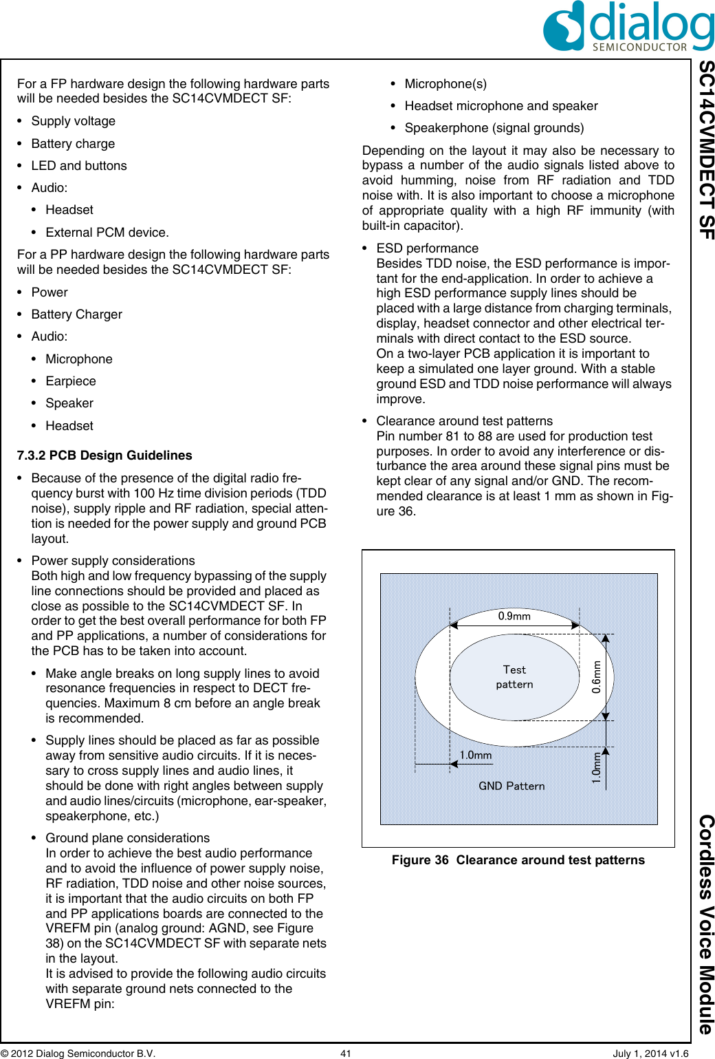
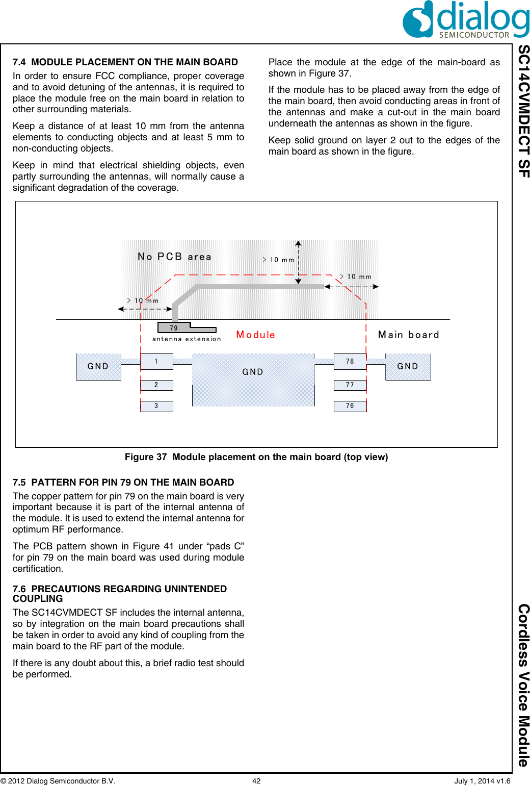
![SC14CVMDECT SF Cordless Voice Module© 2012 Dialog Semiconductor B.V. 43 July 1, 2014 v1.68.0 Example Application DiagramFigure 38 Reference diagram example5544332211D DC CB BA AAGNDUTXURXP0[2]P0[3]P0[4]P0[5]P0[6]P0[7]P1[0P1[1]P1[2]P1[3]P1[4]P1[5]PONCHARGEP2[0]P2[1]P2[2]P2[3]P2[4]P2[5]P2[6]P2[7]MIChPAOUTnPAOUTpP3[2]P3[3]P3[4]P3[5]P3[6]P3[7]JTAGTitle :Doc. Nr. Rev:Date: Sheet: of Dialog Semiconductor .Het Zuiderkruis 535215 MV 's-Hertogenboschtel. (+31) 73 6408822fax. (+31) 73 6408823Designer: 0.1SC14CVMDECT_SF01_RD11Wednesday, November 28, 2012F v D<OrgName>Title :Doc. Nr. Rev:Date: Sheet: of Dialog Semiconductor .Het Zuiderkruis 535215 MV 's-Hertogenboschtel. (+31) 73 6408822fax. (+31) 73 6408823Designer: 0.1SC14CVMDECT_SF01_RD11Wednesday, November 28, 2012F v D<OrgName>Title :Doc. Nr. Rev:Date: Sheet: of Dialog Semiconductor .Het Zuiderkruis 535215 MV 's-Hertogenboschtel. (+31) 73 6408822fax. (+31) 73 6408823Designer: 0.1SC14CVMDECT_SF01_RD11Wednesday, November 28, 2012F v D<OrgName>R91KC4DNAR20RLSR11122R70RSC14CVMDECT SF01U1SC14WSMDATA_SF01P1[2]/INT2/SK36VBATSW 62P0[4]/SPI_EN43RSTn52CP_VOUT126P1[5]/INT5/RDI/VDDE33P2[6]WTF_IN39P0[1]/URX47VBATIN 63P3[0]/PAOUTn/DP027P2[7]/BXTAL32P1[4]/INT4/TDOD34P1[1]/INT1/LE37P0[0]/UTX48JTAG53P3[1]/PAOUTp/DP124P1[6] / PON29P1[7] / CHARGE23P2[4]/SCL1/PCM_DO/DP355VDDOUT 61P2[5]/PCM_FSC/SF54VDDPA 25CHARGE_CTRL 22P0[7]/SPI_DI/PWM140SOCp 17P1[0]/INT0/ADC116ULP_PORT31ULP_XTAL30P0n 4P2[3]/SDA1/PCM_DI/DP256P1[3]/INT3/SIO35P0[6]/SPI_DO41LSRn 13P3[3]/ADC015DC_CTRL 21VREFm 11LSRp 12P3[7]/RINGp66DC_SENSE 19DC_I 20P2[2]/PCM_CLK/CLK10057RFP0n 5MICh 10P3[5]/RINGING/RINGOUT68RFP0 3P2[1]/ECZ2/PWM1/LED458VREFp 7MICp/CIDINn 8P3[2]/CIDINp65P3[6]RINGn67P3[4]/PARADET69P2[0]/ECZ1/PWM0/LED359RF0 75MICn/CIDOUT 9P0 2RF1 73P0[5]/SPI_CLK42VBATIN 64P0[3]/URX2/SCL244 P0[2]/UTX2/SDA246GND1GND14GND38GND49GND50GND60GND51GND6SOCn/GND 18GND28GND45GND70GND71GND72GND74GND76GND77GND78GND80C131uFR51KMIC11122C9DNAC1210pF+C1122uFR30RR610RC80,.1uFR10RC5DNAC1510pFJ112C31uFC6DNAC10DNAJ212345R81KR40RC70,.1uFinternal](https://usermanual.wiki/Dialog-Semiconductor/SC14S.user-manual-CVMDECT/User-Guide-2324864-Page-43.png)