Dialog Semiconductor SC14S DECT Module User Manual SC14SPNODE SF 1V6
Dialog Semiconductor BV DECT Module SC14SPNODE SF 1V6
UserManual.wiki
>
Dialog Semiconductor
>
SC14S User Manual
>
user manual SPNODE
Contents
1.
user manual CVMDECT
2.
user manual SPNODE
3.
Rev_User Manual_68-2959-01_Bx_101217.pdf
user manual SPNODE
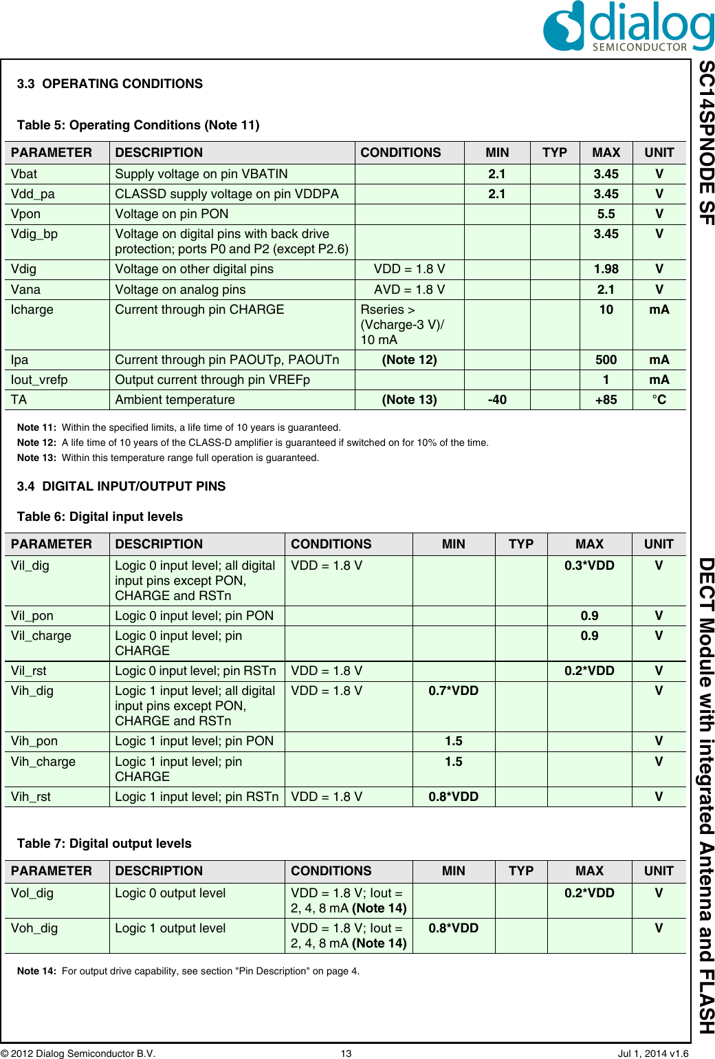
Navigation menu
Upload a User Manual
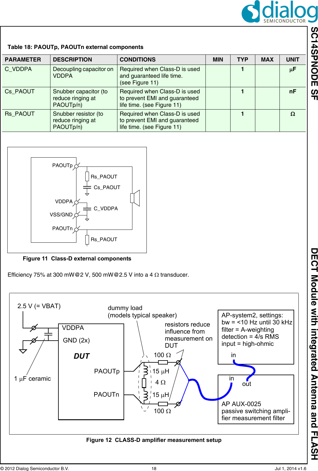
Namespaces
Wiki Guide
HTML
PDF
Info
Views
User Manual
Discussion / Help
Navigation
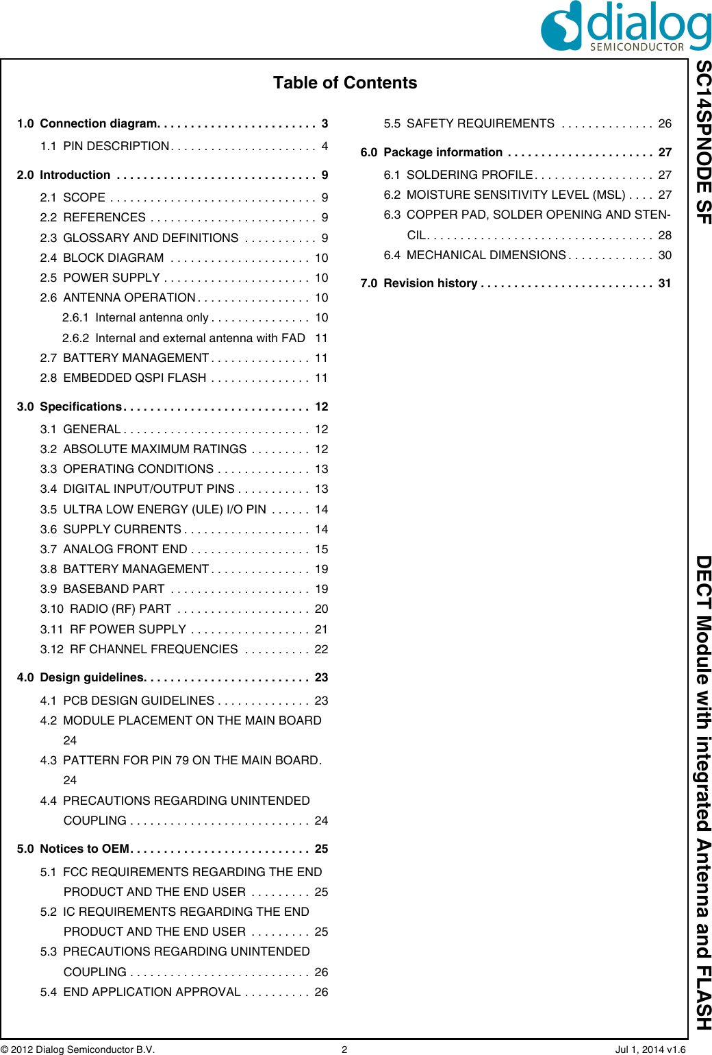
![SC14SPNODE SF DECT Module with integrated Antenna and FLASH© 2012 Dialog Semiconductor B.V. 3 Jul 1, 2014 v1.61.0 Connection diagramFigure 1 Connection diagram (top view, leads face down)Order numbers:SC14SPNODE SF01T (tray, MPQ = 600 pcs)1232221201918171615141312111098765432274948474645444342414039383736353433323130292826252472505152535455565758596061626364656667686970717980GNDPARADET/P3[4]P2[0]/ECZ1/PWM0/LED3GNDTP1RINGOUT/RINGING/P3[5]GNDRFP0P0GNDGNDADC0/P3[3]LSRn/LINEOUT/AGNDLSRp/LINEOUT/AGNDVREFmMICn/CIDOUTMICp/CIDINnVREFpMICh/LINEINCIDINp/P3[2]RINGp/P3[7]RINGn/P3[6]DC_IDC_SENSESOCnSOCpADC1/INT0/P1[0]DC_CTRLVDDE/RDI/INT5/P1[5]ULP_PORTULP_XTALPON/P1[6]CP_VOUT1GNDDP0/PAOUTn/P3[0]VDDPADP1/PAOUTp/P3[1]CHARGE/P1[7]CHARGE_CTRLVBATSWVBATINVBATINVDDOUTGNDSIO/INT3/P1[3]TDOD/INT4/P1[4]BXTAL/INT7/P2[7]SK/INT2/P1[2]LE/INT1/P1[1]P0[7]/PWM1SPI_DIP0[6]/SPI_DOGNDWTF_IN/P2[6]P0[4]/SPI_ENP0[3]/SCL2/URX2P0[5]/SPI_CLKP0[2]/SDA2/UTX2P0[1]/PWM0/URXP0[0]/UTXGNDRSTnJTAGSF/P2[5]/PCM_FSCDP3/P2[4]/SCL1/PCM_DODP2/P2[3]/SDA1/PCM_DICLK100/P2[2]/PCM_CLKP2[1]/ECZ2/PWM1/LED4RFP0nP0nRF1GNDRF0GNDGNDGNDGNDGND787776757473GNDGNDGND8182838487888586](https://usermanual.wiki/Dialog-Semiconductor/SC14S.user-manual-SPNODE/User-Guide-2324865-Page-3.png)
![SC14SPNODE SF DECT Module with integrated Antenna and FLASH© 2012 Dialog Semiconductor B.V. 4 Jul 1, 2014 v1.61.1 PIN DESCRIPTIONTable 1: Pin descriptionPinModule Pin name(Note 1)In/OutIoutDrive(mA)Reset State (Note 2)Description1 GND - - - Ground2 P0 O 8 Hi-Z Control port for FAD. See 2.63 RFP0 O 8 Hi-Z Control port for FAD. See 2.64 P0n O 8 Hi-Z Control port for FAD. See 2.65 RFP0n O 8 Hi-Z Control port for FAD. See 2.66 GND - - - Ground7 VREFp O - I Positive microphone supply voltage8CIDINnMICpI - I INPUT. Caller-id opamp negative input with switchable input protec-tion enabled from start-up.INPUT. Positive microphone input.9CIDOUT/MICnIO - I OUTPUT. Caller-id opamp output to ADC. INPUT. Negative microphone input.10 MICh/LINEINI - I INPUT. Headset microphone input with fixed input protectionINPUT. Line interface input with fixed input protection11 VREFm - - - Negative microphone reference. This pin must also be connected to GND ground, but make sure that the microphone ground is directly routed to VREFm (VREFm is the star point).12 LSRp/LINEOUT/AGNDO - O OUTPUT. Positive loudspeaker outputOUTPUT. To Line interface.OUTPUT. Buffered analog ground (0.9 V) if LSRP_MODE = 00.13 LSRn/LINEOUT/AGNDO - O OUTPUT. Negative loudspeaker output.OUTPUT. To Line interface.OUTPUT. Buffered analog ground (0.9 V) if LSRN_MODE = 00.14 GND - - - Ground15 P3[3]/ADC0IO 8 I INPUT/OUTPUT with selectable pull up/down resistor.INPUT. ADC0 input to ADC with programmable input protection enabled from reset. (Note 4)16 P1[0]/INT0/ADC1IO 2 I-PU INPUT/OUTPUT with selectable pull up/down resistor.INPUT. Keyboard input interrupt.INPUT. ADC1 input to ADC with programmable input protection enabled from reset. (Note 4)17 SOCp I - I Battery State Of Charge positive input.Connect to GND if not used.18 SOCn I - I Battery State Of Charge negative input. Star point connected to the SOC resistor. Connect to GND if not used.19 DC_SENCE I I INPUT. Voltage sense input. Connected via a resistor divider to the output of the DC/C converter. Maximum 1.27 VConnect to GND if not used.20 DC_I I I Current sense input of DC/DC converter. Connect to GND if not used21 DC_CTRL O 2 O-PD(fixed 100k pull-down)OUTPUT. Switching clock for the DC/DC converter, this pad is sup-plied with VBAT.Leave unconnected if not used.](https://usermanual.wiki/Dialog-Semiconductor/SC14S.user-manual-SPNODE/User-Guide-2324865-Page-4.png)
![SC14SPNODE SF DECT Module with integrated Antenna and FLASH© 2012 Dialog Semiconductor B.V. 5 Jul 1, 2014 v1.622 CHARGE_CTRL O 1 O-0 ANALOG OUTPUT. Charge control pin. Supplied by internal VBAT if device is off else from AVD.Leave unconnected if not used.23 CHARGE / P1[7] I - I-PD(270k fixed pull-down)INPUT. Charger connected indication and supply voltage for power management. Switches on the device if voltage > Vih_a3pad. Must be connected to charger via resistor R>(Vcharger_max-3 V)/10 mA (round to next largest value in range). An internal 10 ms hold circuit keeps device on if the charger voltage ripple momentarily drop below Vil_charge. This eliminates the use of expensive ripple filter. If used as port pin, the maximum input switching speed of this pin is 100 kHz. Leave unconnected if not used.24 PAOUTpP3[1]DP1IO 500 O-0 (5k fixed pull-down)OUTPUT. CLASSD positive output to loudspeaker.OUTPUT. General purpose output.OUTPUT. DIP port DP125 VDDPA I - - CLASSD Audio Amplifier supply voltage up to 3.45 V.GND or leave unconnected if PAOUT/P3[1:0] ports are not used.26 CP_VOUT1 O - I Charge Pump Output 1.A capacitor of 1 F to GND is internally connected to this pin.27 PAOUTnP3[0]DP0IO 500 O-0 (5k fixed pull-down)OUTPUT. CLASSD negative output to loudspeaker.OUTPUT. General purpose output.OUTPUT. DIP port DP028 GND - - - Ground29 PON/P1[6]I-I (270k fixed pull-down)INPUT. Power on, Switches on the device if Voltage > Vih_a3pad. May be directly connected to VBAT. If used as port pin, the maxi-mum input switching speed of this pin is 100 kHz.30 ULP_XTAL I - I 32.768 kHz XTAL clock input. Connect to GND if not used. (Note 7)31 ULP_PORT I - I Ultra Low Power Port Pin. Connect to GND if not used. (Note 7)32 P2[7]/INT7BXTALIO 8 I-PU INPUT/OUTPUT with selectable pull up/down resistor.INPUT. Keyboard Interrupt.connected to P1[2] or P2[7].OUTPUT. Digital buffered Xtal oscillator. This pin is not optimized as reference clock for external RF devices.33 P1[5]/INT5/RDI/VDDEIO 8 O-1 INPUT/OUTPUT with selectable pull up/down resistor.INPUT. Keyboard input interrupt.INPUT. BMC Receive data (for monitoring/external radio).OUTPUT. P1[5] Used for supply of external EEPROM34 P1[4]/INT4/TDODIO 1/2 I-PD INPUT/OUTPUT with selectable pull up/down resistor. 1 mA or 2 mA mode used to bias external NPN transistor without external resistor.INPUT. Keyboard input interrupt.OUTPUT. BMC transmit digital data.35 P1[3]/INT3/SIOIO 1/2 I-PD INPUT/OUTPUT with selectable pull up/down resistor.1 mA or 2 mA mode used to bias external NPN transistor without external resistor.INPUT. Keyboard input interrupt. INPUT/OUTPUT. MicroWire data (for monitoring/external radio).36 P1[2]/INT2/SKIO 2 I-PD INPUT/OUTPUT with selectable pull up/down resistor.INPUT. Keyboard input interrupt.OUTPUT. MicroWire clock (for monitoring/external radio).Table 1: Pin description (Continued)PinModule Pin name(Note 1)In/OutIoutDrive(mA)Reset State (Note 2)Description](https://usermanual.wiki/Dialog-Semiconductor/SC14S.user-manual-SPNODE/User-Guide-2324865-Page-5.png)
![SC14SPNODE SF DECT Module with integrated Antenna and FLASH© 2012 Dialog Semiconductor B.V. 6 Jul 1, 2014 v1.637 P1[1]/INT1/LEIO 2 I-PU INPUT/OUTPUT with selectable pull up/down resistor.INPUT. Keyboard input interrupt.INPUT. MicroWire latch enable. (for monitoring/external radio).38 GND - - - Ground39 P2[6]/WTF_INIO 2 I-PU INPUT/OUTPUT with selectable pull up/down resistor.OUTPUT. Gen2DSP enable signal used to monitor DSP load40 P0[7]/SPI_DI/PWM1IO 8 I-PU INPUT/OUTPUT with selectable pull up/down resistor.INPUT. SPI data input.OUTPUT. Timer 0 PWM 1 output.41 P0[6]/SPI_DOIO 8 I-PU INPUT/OUTPUT with selectable pull up/down resistor.OUTPUT. SPI data output.42 P0[5]/SPI_CLKIO 8 I-PU INPUT/OUTPUT with selectable pull up/down resistor.INPUT/OUTPUT. SPI clock.43 P0[4]/SPI_ENIO 8 I-PU INPUT/OUTPUT with selectable pull up/down resistor.INPUT/OUTPUT. SPI clock enable. Active low.44 P0[3]/SCL2/URX2IO 8 I-PU INPUT/OUTPUT with selectable pull up/down resistor.INPUT/OUTPUT. ACCESS bus 2 clock with programmable Push-pull or open drain. In open drain mode, SCL2 is monitored to sup-port bit stretching by a slave.INPUT. UART2 receive data45 GND - - - Ground46 P0[2]/SDA2/UTX2IO 8 I-PU INPUT/OUTPUT with selectable pull up/down resistor.INPUT/OUTPUT. ACCESS bus 2 data with programmable.Push-pull or open drain.OUTPUT. UART2 transmit data47 P0[1]/URX/PWM0IO 8 I-PD(10k)INPUT/OUTPUT with selectable pull up/down resistor.INPUT. UART receive data.OUTPUT. Timer 0 PWM048 P0[0]/UTXO 8 I-PU INPUT/OUTPUT with selectable pull up/down resistor.OUTPUT. UART transmit data.49 GND - - - Ground50 GND - - - Ground51 GND - - - Ground52 RSTn I 1 I-PU(200k pull-up)Active low Reset input with Schmitt-trigger input, open-drain output and pull up resistor to internal VDD. Input may not exceed 2.0 V. An internal capacitor of 47 nF is mounted on this pin.53 JTAG IO 8 I-PU JTAG-SDI+; one wire Debug interface with open-drain.Requires external 1 k Pull-up to VDD.54 P2[5]/PCM_FSC/SFIO 8 I-PU INPUT/OUTPUT with selectable pull up/down resistor.INPUT/OUTPUT. PCM Frame Sync.OUTPUT. S-field Sync found signal indicating the 00 or 11 pream-ble to unique word transition with 96 ns resolution. Used for debug-ging purposes.55 P2[4]/SCL1/PCM_DO/DP3IO 8 I-PU INPUT/OUTPUT with selectable pull up/down resistor.INPUT / OUTPUT. ACCESS bus 1 clock with programmable Push-pull or open drain. In open drain mode, SCL1 is monitored to sup-port bit stretching by a slave.OUTPUT. PCM data output.OUTPUT. DIP port DP3. Table 1: Pin description (Continued)PinModule Pin name(Note 1)In/OutIoutDrive(mA)Reset State (Note 2)Description](https://usermanual.wiki/Dialog-Semiconductor/SC14S.user-manual-SPNODE/User-Guide-2324865-Page-6.png)
![SC14SPNODE SF DECT Module with integrated Antenna and FLASH© 2012 Dialog Semiconductor B.V. 7 Jul 1, 2014 v1.656 P2[3]/SDA1/PCM_DI/DP2IO 8 I-PU INPUT/OUTPUT with selectable pull up/down resistor.INPUT / OUTPUT. ACCESS bus 1 data with programmable Push-pull or open drain.INPUT. PCM data input.OUTPUT. DIP port DP2. 57 P2[2]/PCM_CLK/CLK100I/O 8 I-PD INPUT/OUTPUT with selectable pull up/down resistor.INPUT/OUTPUT. PCM clock.OUTPUT. DIP 100 Hz output.58 P2[1]/ECZ2/PWM1/LED4IO 8 I INPUT/OUTPUT with selectable pull up/down resistor.OUTPUT. Gen2DSP output port.OUTPUT. Timer 0 PWM 1 output.LED4: 2.5 mA/5 mA LED current sink.59 P2[0]/ECZ1/PWM0/LED3IO 8 I INPUT/OUTPUT with selectable pull up/down resistor.OUTPUT. Gen2DSP output port.OUTPUT. Timer 0 PWM 0 output.LED3: 2.5 mA/5 mA LED current sink.60 GND - - - Ground61 VDDOUT - - - Test purpose only. Must be left unconnected. See 2.562 VBATSW Test purpose only. Must be left unconnected. See 2.563 VBATIN I - - Main supply voltage < 3.45 V. See 2.564 VBATIN I - - Main supply voltage < 3.45 V. See 2.565 P3[2]/CIDINp/IO 8 I INPUT/OUTPUT with selectable pull up/down resistor.INPUT. Caller-id opamp positive input with switchable input protec-tion enabled from start-up. 66 P3[7]/RINGpIO 4 I INPUT/OUTPUT with selectable pull up/down resistor.ANALOG INPUT. Positive ringing signal opamp input with switcha-ble input protection.67 P3[6] /RINGnIO 4 I INPUT/OUTPUT with selectable pull up/down resistor.ANALOG INPUT. Negative ringing signal opamp input with switcha-ble input protection.68 P3[5]/RINGOUT/RINGINGIO 4 I INPUT/OUTPUT with selectable pull up/down resistor.OUTPUT. Ringing opamp output to ADC.INPUT. Ringer signal detection input to capture timers and ADC.69 P3[4]/PARADETIO 8 I INPUT/OUTPUT with selectable pull up/down resistor.ANALOG INPUT. Parallel set detection input to ADC with switcha-ble input protection.70 GND - - - Ground71 GND - - - Ground72 GND - - - Ground73 RF1 - - - RF signal for external antenna. See 2.674 GND - - - Ground75 RF0 - - - RF signal for external antenna. See 2.676 GND - - - Ground77 GND - - - Ground78 GND - - - Ground79 TP1 - - - Tuning point for internal antenna. Follow instructions of section 4.3.80 GND - - - GroundTable 1: Pin description (Continued)PinModule Pin name(Note 1)In/OutIoutDrive(mA)Reset State (Note 2)Description](https://usermanual.wiki/Dialog-Semiconductor/SC14S.user-manual-SPNODE/User-Guide-2324865-Page-7.png)
![SC14SPNODE SF DECT Module with integrated Antenna and FLASH© 2012 Dialog Semiconductor B.V. 8 Jul 1, 2014 v1.6Note 1: “NC” means: leave unconnected. “GND” means internally connected to the module ground plane. Every GND pin should be connected to the main PCB.ground plane. Note 2: All digital inputs have Schmitt trigger inputs. After reset all I/Os are set to input and all pull-up or pull-down resistors are enabled unless oth-erwise specified. PU = Pull-up resistor enabled, PD = Pull-down resistor enabled, I = input, O = output, Hi-Z = high impedance, 1 = logic HIGH level, 0 = logic LOW levelRefer also to Px_DIR_REGs for INPUT/OUTPUT and Pull-up/Pull-down configurationsNote 3: Back drive protected pins allow always interfacing with devices up to a supply voltage of 3.45 V.If PAD_CTRL_REG[xxx_OD] bit is set then1) the internal Pull-up resistors are always disabled to prevent currents from 1.8 V < Vin < 3.45 V to VDD.2) If port is set to output, the output is always configured as open drain to allow the output level to reach Vin >1.8 V. The external pull-up resistor value determines the rise time of the signal.Note 4: For base station applications with high line input voltages, an input protection on all ADC inputs can be enabled with AD_CTRL_REG[ADCx_PR_DIS] =’0’. To limit the input current as specified in chapter “specifications”, an external resistor must placed in series with the ADC inputs. With the input protection enabled, the ADC is linear from 0 to 0.9 V. With ADCx_PR_DIS=’1’ the ADC0 and ADC1 are linear from 0 V to 1.8 V.Note 5: In digital mode extra static VDDPA current will flow (See Supply currents (indicative value) (table 9, page 14)). So the digital mode is not recommended in portable applications.The reason for this output overvoltage protection is that a speaker is an inductor (which can store energy). In case the battery is removed from the handset while handsfree speaker is active, the battery voltage could become too high when the inductor releases its energy to the battery (which is not present anymore as a buffer). To prevent this electrical overstress situa-tion, the overvoltage protection is added.Note 6: This pin description describes all function that is supported by hardware. Supported pin function depends on installed software.Note 7: All ULP pins use snap-back devices as ESD protection, which (when triggered) have a holding voltage below the typical battery voltage. This means that the snap-back device of a ULP pin may remain conductive, when triggered while the pin is directly connected to the battery voltage. If any of the ULP pins are directly or indirectly electrically accessible on the outside of the application, system level ESD precau-tions must be taken to ensure that the snap-back device is not triggered while in active mode, to prevent the chip from being damaged. 81-88 TP2 to TP9 NC Must be left unconnected. See section 4.1 and Figure 15.Table 1: Pin description (Continued)PinModule Pin name(Note 1)In/OutIoutDrive(mA)Reset State (Note 2)Description](https://usermanual.wiki/Dialog-Semiconductor/SC14S.user-manual-SPNODE/User-Guide-2324865-Page-8.png)
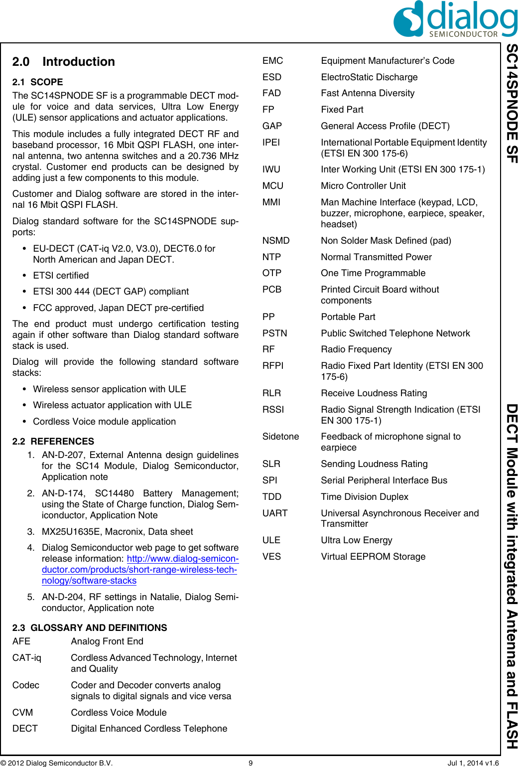
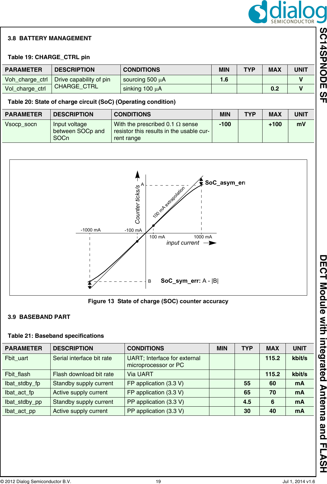
![SC14SPNODE SF DECT Module with integrated Antenna and FLASH© 2012 Dialog Semiconductor B.V. 11 Jul 1, 2014 v1.62.6.2 Internal and external antenna with FADFigure 5 shows one external antenna that is connectedto RF1 of the SC14SPNODE SF. This configurationsupports the FAD function. In this case pins RFP0,RFP0n, P0 and P0n must be left unconnected. Thesoftware patch code is not needed if theSC14SPNODE SF is operated as FP.2.7 BATTERY MANAGEMENTFigure 6 shows a handset application with NiMH. SOC(State Of Charge) is used to measure the amount ofcharge in the rechargeable batteries.Figure 7 shows an FP application. The FP uses anexternal LDO, so the SOC pins are not used and canbe connected to GND.The SOC circuit is used to very accurately determinethe amount of charge in rechargeable batteries as wellas the discharge state of Alkaline batteries. This infor-mation is essential for the battery charging algorithmand necessary for battery status indication to the user.Detailed information can be found in AN-D-174 (seeReference [2]).Pin CHARGE_CTRL is driven high when either“sensed voltage on the VBAT pin” is lower than thevoltage setting (defined by the module hardware) or“sensed current via SOCp” is lower than the currentsetting (defined by the module hardware). PinCHARGE_CTRL can drive up to 500 A as source cur-rent (see Table 19). 2.8 EMBEDDED QSPI FLASHThe SC14SPNODE SF has a QSPI FLASH with typenumber MX25U1635E as embedded FLASH. Pleaserefer to Reference [3] for detailed specifications.The MX25U1635E has an OTP area, a part of whichhas already been factory programmed by Dialog fortuning purposes.Table 2 shows the production parameters and the rela-tion between the SC14SPNODE SF register addressand the OTP address.The OTP addresses from 0x020 to 0x1FF are availablefor write access before locking the OTP.Figure 5 One external antennaFigure 6 Handset (PP) application with 2x NiMHExternalAntennaRF1100CHARGE_CTRL1k1k0.1SOCCHARGESOCpSOCnVsupply VBAT INSC14SPNODEFigure 7 Base station (FP) applicationCHARGE_CTRL1kSOCCHARGESOCpSOCnVsupply VBAT INLDOSC14SPNODETable 2: SC14SPNODE production parametersRegister name SC14SPNODE address OTP address Alignment Spec.RF_BURST_MODE_CTRL_REG[MODINDEX] 0xFF7053[5:0] 0x05 340 kHz to 370 kHzCLK_FREQ_TRIM_REG (lsb) 0xFF400A 0x06 20.736 MHz +/- 1 ppmCLK_FREQ_TRIM_REG (msb) 0xFF400B 0x07BANDGAP_REG 0xFF4810 0x08 1.8 V +/- 1%](https://usermanual.wiki/Dialog-Semiconductor/SC14S.user-manual-SPNODE/User-Guide-2324865-Page-11.png)
![SC14SPNODE SF DECT Module with integrated Antenna and FLASH© 2012 Dialog Semiconductor B.V. 14 Jul 1, 2014 v1.63.5 ULTRA LOW ENERGY (ULE) I/O PIN3.6 SUPPLY CURRENTSNote 15: PAOUTp and PAOUTn have internal fixed resistors connected to VSSPA. The values are 5 k if CLASSD[CLASSD_VOUT] = 01, else 6k. So in digital mode with a ‘1’ on output a small static current will flow.Table 8: ULP_PORT specificationsPARAMETER DESCRIPTION CONDITIONS MIN TYP MAX UNITSVil_ulp Logic 0 input level; pin ULP_PORTVbat = 2.1 V to 3.45 V0.2*Vbat VVih_ulp Logic 1 input level; pin ULP_PORTVbat = 2.1 V to 3.45 V0.8*Vbat VVol_ulp Logic 0 output level; pin ULP_PORTIout = 1 mA, Vbat = 2.4 V0.2*Vbat VVoh_ulp Logic 1 output level; pin ULP_PORTIout = 1 mA, Vbat = 2.4 V0.8*Vbat VIpull_up_ulp Input current with pull up enabled; pin ULP_PORTVin = GND 2.5 AIpull_down_ulp Input current with pull down enabled; pin ULP_PORTVin = Vbat; Vbat = 2.1 V to 3.45 V2.5 ATable 9: Supply currents (indicative value)PARAMETER DESCRIPTION CONDITIONS MIN TYP MAX UnitIavd_pa CLASSD normal mode supply current at AVDCLASSD_PD=0 3.5 mAIavd_paport CLASSD digital port mode supply current at AVD(P3_0_MODE = 00 or P3_1_MODE = 00) and CLASSD_PD=1. (Note 15)5A](https://usermanual.wiki/Dialog-Semiconductor/SC14S.user-manual-SPNODE/User-Guide-2324865-Page-14.png)
![SC14SPNODE SF DECT Module with integrated Antenna and FLASH© 2012 Dialog Semiconductor B.V. 15 Jul 1, 2014 v1.63.7 ANALOG FRONT ENDNote 16: BANDGAP_REG will be tuned at the factory.Note 17: 0 dBm0 on COUT = -3.14 dB of max PCM value. COUT is CODEC output in test modeNote 18: Trimming possibility is foreseen. At system production the bandgap reference voltage can be controlled within 2% accuracy and data can be stored in Flash. Either AVD or VREF can be trimmed within 2% accuracy. If AVD is trimmed VREF will be within 2% accuracy related to either AVD. Or vice versa VREF can be trimmed. For Vref trimming measure VREFp, VREFm) and update BANDGAP_REG[3..0].Note 19: Vrefm is a clean ground input and is the 0 V reference.Table 10: Microphone amplifierPARAMETER DESCRIPTION CONDITIONS MIN TYP MAX UNITVmic_0dB_unt Untrimmed differen-tial RMS input volt-age between MICp and MICn (0 dBm0 reference level) (Note 8)0 dBm0 on COUT(Note 17)MIC_GAIN[3:0] = 0, @ 1020 Hz;Tolerance:• 13% when untrimmed (BANDGAP_REG=8) (Note 16)• 6% when trimmed (Note 18)114 131 149 mVRin_mic Resistance of acti-vated microphone amplifier inputs (MICp, MICn and MICh) to internal GND (Note 8)75 150 kVmic_offset Input referred DC-off-set (Note 8)MIC_GAIN[3..0] = 11113 sigma deviation limits-2.6 +2.6 mVTable 11: Microphone amplifier (Operating Condition)PARAMETER DESCRIPTION CONDITIONS MIN TYP MAX UNITVmic_cm_level MICp and MICn com-mon mode voltageMICp and MICn are set to GND with internal resistors (Rin_mic). If DC coupled the input voltage must be equal to this voltage.(0.9 V/1.5)* VREFp VTable 12: Microphone supply voltagesPARAMETER DESCRIPTION CONDITIONS MIN TYP MAX UNITVref_unt VREFp-VREFm untrimmed (Note 19)ILOAD = 0 mA BANDGAP_REG = 8 (Note 18)1.41 1.5 1.59 VRout_vrefp VREFp output resistanceFigure 8 1Nvrefp_idle Peak noise on VREFp-VREFm(Note 8)CCITT weighted -120 dBVPSRRvrefp Power supply rejec-tion Vref output (Note 8)See Figure 8, AVD toVREFp/m, f = 100 Hz to 4 kHzBANDGAP_REG[5:4] = 340 dB](https://usermanual.wiki/Dialog-Semiconductor/SC14S.user-manual-SPNODE/User-Guide-2324865-Page-15.png)
![SC14SPNODE SF DECT Module with integrated Antenna and FLASH© 2012 Dialog Semiconductor B.V. 16 Jul 1, 2014 v1.6Note 20: 0 dBm0 on CIN = -3.14 dB of max PCM value.Table 13: VREFp load circuitPARAMETER DESCRIPTION CONDITIONS MIN TYP MAX UNITCload_vrefp VREFp (parasitic) load capacitance20 pFIout_vrefp VREFp output current 1mAFigure 8 VREFp load circuitCload_vrefpVREFpVREFmIout_vrefpRout_vrefpTable 14: LSRp/LSRn outputsPARAMETER DESCRIPTION CONDITIONS MIN TYP MAX UNITVlsr_0dB_unt Untrimmed differen-tial RMS output volt-age between LSRp and LSRn in audio mode (0 dBm0 refer-ence level)0 dBm0 on CIN (Note 20), LSRATT[2:0] = 001, @ 1020 Hz Load circuit A (see Figure 9, Table 15) with RL1= , Cp1 or load circuit B (see Figure 10) with RL2, Cp2 and Cs2Tolerance:• 13% when untrimmed (BANDGAP_REG=8)• 6% when trimmed (Note 18)621 714 807 mVRout_lsr Resistance of acti-vated loudspeaker amplifier outputs LSRp and LSRn1Vlsr_dc DC offset between LSRp and LSRn (Note 8)LSRATT[2:0] = 3RL1 = 28 3 sigma deviation limits-20 20 mV](https://usermanual.wiki/Dialog-Semiconductor/SC14S.user-manual-SPNODE/User-Guide-2324865-Page-16.png)
![SC14SPNODE SF DECT Module with integrated Antenna and FLASH© 2012 Dialog Semiconductor B.V. 17 Jul 1, 2014 v1.6Note 21: Clipping of the outputs occurs when the VDDPA drops and the following conditions becomes true. If CLASSD_CTRL_REG[CLASSD_CLIP] is not equal to zero then upon a programmable number of clipping occurrences a CLASSD_INT is generated:The software can stop clipping by reducing the gain via the GENDSP:Clipping occurs ifTable 15: LSRp/LSRn load circuitsPARAMETER DESCRIPTION CONDITIONS MIN TYP MAX UNITCp1_Rl1_inf Load capacitance see Figure 9, RL1 = 30 pFCp1_Rl1_1k Load capacitance see Figure 9, RL1 1 k100 pFRl1 Load resistance 28 Cp2 Parallel load capacitancesee Figure 10 30 pFCs2 Serial load capacitance 30 FRl2 Load resistance 600 Figure 9 Load circuit A: Dynamic loudspeakerRL1 Cp1LSRpLSRnFigure 10 Load circuit B: Piezo loudspeakerCs2LSRpLSRnRL2Cp2Table 16: PAOUTp, PAOUTn outputsPARAMETER DESCRIPTION CONDITIONS MIN TYP MAX UNITVpa_4v Differential rms output voltage between PAOUTp and PAOUTnTrimmed bandgapinput = 0 dBm0, 1 kHz (Note 17)Output low-pass filteredCLASSD_VOUT = 00.985 VrmsVpa_6v As aboveCLASSD_VOUT = 11.478 VrmsZload_pa_4v Speaker impedance, connected between PAOUTp and PAOUTnWith these values, the peak cur-rents stays within the operating range.4Zload_pa_6v 6Table 17: PAOUTp, PAOUTn outputs (Note 21)PARAMETER DESCRIPTION CONDITIONS MIN TYP MAX UNITRout_pa Differential output resistance between PAOUTp and PAOUTnSee (Note 21) 1peak LowPassFiltered PAOUTp PAOUTm–VDDPA VSSPA–-----------------------------------------------------------------------------------------------------------------------ZloadZload Rout_pa+-------------------------------------------](https://usermanual.wiki/Dialog-Semiconductor/SC14S.user-manual-SPNODE/User-Guide-2324865-Page-17.png)
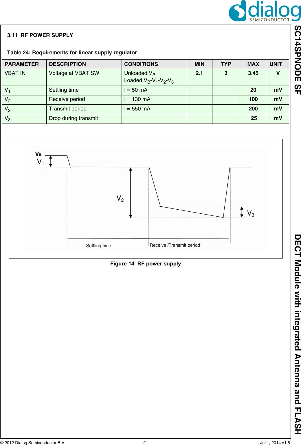
![SC14SPNODE SF DECT Module with integrated Antenna and FLASH© 2012 Dialog Semiconductor B.V. 20 Jul 1, 2014 v1.63.10 RADIO (RF) PARTStandards compliancy: ETS 301 406 (former TBR6).Table 22: Radio specificationsPARAMETER DESCRIPTION CONDITIONS MIN TYP MAX UNITP_Rx Receiver sensitivity BER = 0.001; TA = 25 °C -93 -92 -89 dBmP_Rx_T Receiver sensitivity, full temperature rangeBER = 0.001; -40 °C TA 85 °C -94 -87 dBmIPL Intermodulation perform-ance level (EN 301 406 section 4.5.7.6)TA = 25 °C; Pw = -80 dBm; f = 2 channels-35 dBmNTP Normal transmitted power DECT: 250 mW 24 26 dBmJ-DECT: 10 mW average per frame for each slot23 24.5 dBmDECT6.0: 100 mW (max peak)20.0 dBmdPrfpa_T RFPA power variation, full temperature range-40 °C TA +85 °C 2.5 4dBFbit Bit rate GFSK modulation 1.152 Mbit/sBW_Tx Transmitter bandwidth DECT GFSK; NTP = 20 dB1.728 MHzTable 23: RFPA preferred settings for various power modes (PP application)Address (VES) Register / Parameter HPM/U(USA)HPM(Europe)HPM/J(Japan)0x3D RF_BBADC_CTRL_REG 0x0380 0x03A0 0x03980x39 RF_PA_CTRL1_REG 0x09A0 0x0CF0 0x2CE00x3B RF_TEST_MODE2_REG 0x0056 0x0062 0x00680x05 RF_PLL_CTRL2_REG[MODINDEX] 0x25 0x25 0x230x23 Upper RSSI threshold 0x2C N/A 0x280x24 Lower RSSI threshold 0x22 N/A 0x1E](https://usermanual.wiki/Dialog-Semiconductor/SC14S.user-manual-SPNODE/User-Guide-2324865-Page-20.png)
![SC14SPNODE SF DECT Module with integrated Antenna and FLASH© 2012 Dialog Semiconductor B.V. 25 Jul 1, 2014 v1.65.0 Notices to OEMThe end product has to be certified again if it hasbeen programmed with other software than Dialogstandard software stack for portable part and/oruses one or two external antenna(s).5.1 FCC REQUIREMENTS REGARDING THE END PRODUCT AND THE END USERThe end product that the module is integrated into mustbe marked as follows:“Contains Transmitter Module FCC ID: Y82-SC14S /IC: 9576A-SC14S”The literature provided to the end user must include thefollowing wording:FCC compliance statement This device complies with Part 15 of the FCC Rules.]for only portable part.Operation is subject to the following two conditions: (1) this device may not cause harmful interference, and(2) this device must accept any interference received,including interference that may cause undesired opera-tion of the device.Module transmetteur ID IC: 9576A-SC14S.Son fonctionnement est soumis aux deux conditionssuivantes: (1) cet appareil ne doit pas causer d’interfé-rences nuisibles et (2) appareil doit accepter touteinterférence reçue, y compris les interférences qui peu-vent perturber le fonctionnement.Changes or modifications to the equipment notexpressly approved by the Party responsible for com-pliance could void the user's authority to operate theequipment.NOTE: This equipment has been tested and found tocomply with the limits for a Class B digital device, pur-suant to Part 15 of the FCC Rules. These limits aredesigned to provide reasonable protection againstharmful interference in a residential installation. This equipment generate, uses and can radiate radiofrequency energy and, if not installed and used inaccordance with the instructions, may cause harmfulinterference to radio communications. However, thereis no guarantee that interference will not occur in a par-ticular installation. If this equipment does cause harmful interference toradio or television reception, which can be determinedby turning the equipment off and on, the user isencouraged to try to correct the interference by one ormore of the following measures: • Reorient or relocate the receiving antenna • Increase the separation between the equipment and receiver • Connect the equipment into an outlet on a circuit dif-ferent from that to which the receiver is connected. • Consult the dealer or an experienced radio/TV tech-nician for help.Privacy of communications may not be ensured whenusing this phone.5.2 INDUSRY CANADA REQUIREMENTS REGARD-ING THE END PRODUCT AND THE END USERThe host device shall be properly labelled to identifythe modules within the host device. The Industry Can-ada certification label of a module shall be clearly visi-ble at all times when installed in the host device,otherwise the host device must be labelled to displaythe Industry Canada certification number of the mod-ule, preceded by the words "Contains transmitter mod-ule", or the word "Contains", or similar wordingexpressing the same meaning, as follows: Contains transmitter module IC: 9576A-SC14S L'appareil hôte doit être étiqueté comme il faut pourpermettre l'identification des modules qui s'y trouvent.L'étiquette de certification d'Industrie Canada d'unmodule donné doit être posée sur l'appareil hôte à unendroit bien en vue en tout temps. En l'absence d'éti-quette, l'appareil hôte doit porter une etiquette donnantle numéro de certification du module d'Industrie Can-ada, précédé des mots " Contient un module d'émis-sion ", du mot " Contient " ou d'une formulationsimilaire exprimant le même sens, comme suit : Contient le module d'émission IC: 9576A-SC14S This device complies with Industry Canada licence-exempt RSS standard(s). Operation is subject to thefollowing two conditions: (1) this device may not causeinterference, and (2) this device must accept any inter-ference, including interference that may cause unde-sired operation of the device. Le présent appareil est conforme aux CNR d'IndustrieCanada applicables aux appareils radio exempts delicence. L'exploitation est autorisée aux deux condi-tions suivantes : (1) l'appareil ne doit pas produire debrouillage, et (2) l'utilisateur de l'appareil doit acceptertout brouillage radioélectrique subi, même si le brouil-lage est susceptible d'en compromettre le fonctionne-ment.CAN ICES-3 (B)/NMB-3(B)](https://usermanual.wiki/Dialog-Semiconductor/SC14S.user-manual-SPNODE/User-Guide-2324865-Page-25.png)