Dialog Semiconductor SC14S DECT Module User Manual SC14SPNODE SF 1V6
Dialog Semiconductor BV DECT Module SC14SPNODE SF 1V6
Contents
- 1. user manual CVMDECT
- 2. user manual SPNODE
- 3. Rev_User Manual_68-2959-01_Bx_101217.pdf
user manual SPNODE
© 2012 Dialog Semiconductor B.V. 1 www.dialog-semiconductor.com
SC14SPNODE SF DECT Module with integrated Antenna and FLASH
DATASHEET
General description
The SC14SPNODE SF is a member of the Cordless
Module family with an integrated radio transceiver and
baseband processor in a single package. It is designed
for voice and data applications in the DECT frequency
band.
Features
nUltra Low Power, sleep current < 3 A
nETSI (EU-DECT) and FCC (DECT 6.0) certified
nJ-DECT pre-certified
nRF range: 1870 MHz to 1930 MHz
nReceiver sensitivity < -93 dBm
nTransmit power
• EU: 24 dBm: 1881MHz - 1897MHz
• USA: 20 dBm: 1921MH - 1928MHz
• JP: 23 dBm: 1895MHz - 1903MHz
nPower supply voltage: 2.1 V to 3.45 V
nSupports NiMH and Li-Ion batteries
nSmall form factor (19.6 mm x 18.0 mm x 2.7 mm)
nProgram memory available for custom software.
n16 Mbit Flash embedded
nOperating temperature range: -40 °C to +85 °C
________________________________________________________________________________________________
System diagram
PCM
Interface
VoIP
PSTN
Interface
PSTN
SC14
CVMDECT
SC14
SPNODE
Sensor
SC14
SPNODE
Actuator
SC14
CVMDECT
LCD
SC14SPNODE SF
DECT Module with integrated Antenna and FLASH
JUL 1, 2014 V1.6

SC14SPNODE SF DECT Module with integrated Antenna and FLASH
© 2012 Dialog Semiconductor B.V. 2 Jul 1, 2014 v1.6
Table of Contents
1.0 Connection diagram. . . . . . . . . . . . . . . . . . . . . . . . 3
1.1 PIN DESCRIPTION . . . . . . . . . . . . . . . . . . . . . . 4
2.0 Introduction . . . . . . . . . . . . . . . . . . . . . . . . . . . . . . 9
2.1 SCOPE . . . . . . . . . . . . . . . . . . . . . . . . . . . . . . . 9
2.2 REFERENCES . . . . . . . . . . . . . . . . . . . . . . . . . 9
2.3 GLOSSARY AND DEFINITIONS . . . . . . . . . . . 9
2.4 BLOCK DIAGRAM . . . . . . . . . . . . . . . . . . . . . 10
2.5 POWER SUPPLY . . . . . . . . . . . . . . . . . . . . . . 10
2.6 ANTENNA OPERATION . . . . . . . . . . . . . . . . . 10
2.6.1 Internal antenna only . . . . . . . . . . . . . . . 10
2.6.2 Internal and external antenna with FAD 11
2.7 BATTERY MANAGEMENT . . . . . . . . . . . . . . . 11
2.8 EMBEDDED QSPI FLASH . . . . . . . . . . . . . . . 11
3.0 Specifications . . . . . . . . . . . . . . . . . . . . . . . . . . . . 12
3.1 GENERAL . . . . . . . . . . . . . . . . . . . . . . . . . . . . 12
3.2 ABSOLUTE MAXIMUM RATINGS . . . . . . . . . 12
3.3 OPERATING CONDITIONS . . . . . . . . . . . . . . 13
3.4 DIGITAL INPUT/OUTPUT PINS . . . . . . . . . . . 13
3.5 ULTRA LOW ENERGY (ULE) I/O PIN . . . . . . 14
3.6 SUPPLY CURRENTS . . . . . . . . . . . . . . . . . . . 14
3.7 ANALOG FRONT END . . . . . . . . . . . . . . . . . . 15
3.8 BATTERY MANAGEMENT . . . . . . . . . . . . . . . 19
3.9 BASEBAND PART . . . . . . . . . . . . . . . . . . . . . 19
3.10 RADIO (RF) PART . . . . . . . . . . . . . . . . . . . . 20
3.11 RF POWER SUPPLY . . . . . . . . . . . . . . . . . . 21
3.12 RF CHANNEL FREQUENCIES . . . . . . . . . . 22
4.0 Design guidelines. . . . . . . . . . . . . . . . . . . . . . . . . 23
4.1 PCB DESIGN GUIDELINES . . . . . . . . . . . . . . 23
4.2 MODULE PLACEMENT ON THE MAIN BOARD
24
4.3 PATTERN FOR PIN 79 ON THE MAIN BOARD.
24
4.4 PRECAUTIONS REGARDING UNINTENDED
COUPLING . . . . . . . . . . . . . . . . . . . . . . . . . . . 24
5.0 Notices to OEM. . . . . . . . . . . . . . . . . . . . . . . . . . . 25
5.1 FCC REQUIREMENTS REGARDING THE END
PRODUCT AND THE END USER . . . . . . . . . 25
5.2 IC REQUIREMENTS REGARDING THE END
PRODUCT AND THE END USER . . . . . . . . . 25
5.3 PRECAUTIONS REGARDING UNINTENDED
COUPLING . . . . . . . . . . . . . . . . . . . . . . . . . . . 26
5.4 END APPLICATION APPROVAL . . . . . . . . . . 26
5.5 SAFETY REQUIREMENTS . . . . . . . . . . . . . . 26
6.0 Package information . . . . . . . . . . . . . . . . . . . . . . 27
6.1 SOLDERING PROFILE . . . . . . . . . . . . . . . . . . 27
6.2 MOISTURE SENSITIVITY LEVEL (MSL) . . . . 27
6.3 COPPER PAD, SOLDER OPENING AND STEN-
CIL. . . . . . . . . . . . . . . . . . . . . . . . . . . . . . . . . . 28
6.4 MECHANICAL DIMENSIONS . . . . . . . . . . . . . 30
7.0 Revision history . . . . . . . . . . . . . . . . . . . . . . . . . . 31
SC14SPNODE SF DECT Module with integrated Antenna and FLASH
© 2012 Dialog Semiconductor B.V. 3 Jul 1, 2014 v1.6
1.0 Connection diagram
Figure 1 Connection diagram (top view, leads face down)
Order numbers:
SC14SPNODE SF01T (tray, MPQ = 600 pcs)
1
23
22
21
20
19
18
17
16
15
14
13
12
11
10
9
8
7
6
5
4
3
2
27
49
48
47
46
45
44
43
42
41
40
39
38
37
36
35
34
33
32
31
30
29
28
26
25
24
72
50
51
52
53
54
55
56
57
58
59
60
61
62
63
64
65
66
67
68
69
70
71
79
80
GND
PARADET/P3[4]
P2[0]/ECZ1/PWM0/LED3
GND
TP1
RINGOUT/RINGING/P3[5]
GND
RFP0
P0
GND
GND
ADC0/P3[3]
LSRn/LINEOUT/AGND
LSRp/LINEOUT/AGND
VREFm
MICn/CIDOUT
MICp/CIDINn
VREFp
MICh/LINEIN
CIDINp/P3[2]
RINGp/P3[7]
RINGn/P3[6]
DC_I
DC_SENSE
SOCn
SOCp
ADC1/INT0/P1[0]
DC_CTRL
VDDE/RDI/INT5/P1[5]
ULP_PORT
ULP_XTAL
PON/P1[6]
CP_VOUT1
GND
DP0/PAOUTn/P3[0]
VDDPA
DP1/PAOUTp/P3[1]
CHARGE/P1[7]
CHARGE_CTRL
VBATSW
VBATIN
VBATIN
VDDOUT
GND
SIO/INT3/P1[3]
TDOD/INT4/P1[4]
BXTAL/INT7/P2[7]
SK/INT2/P1[2]
LE/INT1/P1[1]
P0[7]/PWM1SPI_DI
P0[6]/SPI_DO
GND
WTF_IN/P2[6]
P0[4]/SPI_EN
P0[3]/SCL2/URX2
P0[5]/SPI_CLK
P0[2]/SDA2/UTX2
P0[1]/PWM0/URX
P0[0]/UTX
GND
RSTn
JTAG
SF/P2[5]/PCM_FSC
DP3/P2[4]/SCL1/PCM_DO
DP2/P2[3]/SDA1/PCM_DI
CLK100/P2[2]/PCM_CLK
P2[1]/ECZ2/PWM1/LED4
RFP0n
P0n
RF1
GND
RF0
GND
GND
GND
GND
GND
78
77
76
75
74
73
GND
GND
GND
81
82
83
84
87
88
85
86
SC14SPNODE SF DECT Module with integrated Antenna and FLASH
© 2012 Dialog Semiconductor B.V. 4 Jul 1, 2014 v1.6
1.1 PIN DESCRIPTION
Table 1: Pin description
Pin
Module
Pin name
(Note 1)
In/
Out
Iout
Drive
(mA)
Reset
State
(Note 2)
Description
1 GND - - - Ground
2 P0 O 8 Hi-Z Control port for FAD. See 2.6
3 RFP0 O 8 Hi-Z Control port for FAD. See 2.6
4 P0n O 8 Hi-Z Control port for FAD. See 2.6
5 RFP0n O 8 Hi-Z Control port for FAD. See 2.6
6 GND - - - Ground
7 VREFp O - I Positive microphone supply voltage
8CIDINn
MICp
I - I INPUT. Caller-id opamp negative input with switchable input protec-
tion enabled from start-up.
INPUT. Positive microphone input.
9CIDOUT/
MICn
IO - I OUTPUT. Caller-id opamp output to ADC.
INPUT. Negative microphone input.
10 MICh/
LINEIN
I - I INPUT. Headset microphone input with fixed input protection
INPUT. Line interface input with fixed input protection
11 VREFm - - - Negative microphone reference. This pin must also be connected to
GND ground, but make sure that the microphone ground is directly
routed to VREFm (VREFm is the star point).
12 LSRp/
LINEOUT/
AGND
O - O OUTPUT. Positive loudspeaker output
OUTPUT. To Line interface.
OUTPUT. Buffered analog ground (0.9 V) if LSRP_MODE = 00.
13 LSRn/
LINEOUT/
AGND
O - O OUTPUT. Negative loudspeaker output.
OUTPUT. To Line interface.
OUTPUT. Buffered analog ground (0.9 V) if LSRN_MODE = 00.
14 GND - - - Ground
15 P3[3]/
ADC0
IO 8 I INPUT/OUTPUT with selectable pull up/down resistor.
INPUT. ADC0 input to ADC with programmable input protection
enabled from reset. (Note 4)
16 P1[0]/
INT0/
ADC1
IO 2 I-PU INPUT/OUTPUT with selectable pull up/down resistor.
INPUT. Keyboard input interrupt.
INPUT. ADC1 input to ADC with programmable input protection
enabled from reset. (Note 4)
17 SOCp I - I Battery State Of Charge positive input.
Connect to GND if not used.
18 SOCn I - I Battery State Of Charge negative input. Star point connected to the
SOC resistor. Connect to GND if not used.
19 DC_SENCE I I INPUT. Voltage sense input. Connected via a resistor divider to the
output of the DC/C converter. Maximum 1.27 V
Connect to GND if not used.
20 DC_I I I Current sense input of DC/DC converter. Connect to GND if not
used
21 DC_CTRL O 2 O-PD
(fixed
100k
pull-
down)
OUTPUT. Switching clock for the DC/DC converter, this pad is sup-
plied with VBAT.
Leave unconnected if not used.

SC14SPNODE SF DECT Module with integrated Antenna and FLASH
© 2012 Dialog Semiconductor B.V. 5 Jul 1, 2014 v1.6
22 CHARGE_CTRL O 1 O-0 ANALOG OUTPUT. Charge control pin. Supplied by internal VBAT
if device is off else from AVD.
Leave unconnected if not used.
23 CHARGE / P1[7] I - I-PD
(270k
fixed
pull-
down)
INPUT. Charger connected indication and supply voltage for power
management. Switches on the device if voltage > Vih_a3pad. Must
be connected to charger via resistor R>(Vcharger_max-3 V)/10 mA
(round to next largest value in range). An internal 10 ms hold circuit
keeps device on if the charger voltage ripple momentarily drop
below Vil_charge. This eliminates the use of expensive ripple filter.
If used as port pin, the maximum input switching speed of this pin is
100 kHz. Leave unconnected if not used.
24 PAOUTp
P3[1]
DP1
IO 500 O-0 (5k
fixed
pull-
down)
OUTPUT. CLASSD positive output to loudspeaker.
OUTPUT. General purpose output.
OUTPUT. DIP port DP1
25 VDDPA I - - CLASSD Audio Amplifier supply voltage up to 3.45 V.
GND or leave unconnected if PAOUT/P3[1:0] ports are not used.
26 CP_VOUT1 O - I Charge Pump Output 1.
A capacitor of 1 F to GND is internally connected to this pin.
27 PAOUTn
P3[0]
DP0
IO 500 O-0 (5k
fixed
pull-
down)
OUTPUT. CLASSD negative output to loudspeaker.
OUTPUT. General purpose output.
OUTPUT. DIP port DP0
28 GND - - - Ground
29 PON/
P1[6]
I-I (270k
fixed
pull-
down)
INPUT. Power on, Switches on the device if Voltage > Vih_a3pad.
May be directly connected to VBAT. If used as port pin, the maxi-
mum input switching speed of this pin is 100 kHz.
30 ULP_XTAL I - I 32.768 kHz XTAL clock input. Connect to GND if not used. (Note 7)
31 ULP_PORT I - I Ultra Low Power Port Pin. Connect to GND if not used. (Note 7)
32 P2[7]/
INT7
BXTAL
IO 8 I-PU INPUT/OUTPUT with selectable pull up/down resistor.
INPUT. Keyboard Interrupt.connected to P1[2] or P2[7].
OUTPUT. Digital buffered Xtal oscillator. This pin is not optimized
as reference clock for external RF devices.
33 P1[5]/
INT5/
RDI/
VDDE
IO 8 O-1 INPUT/OUTPUT with selectable pull up/down resistor.
INPUT. Keyboard input interrupt.
INPUT. BMC Receive data (for monitoring/external radio).
OUTPUT. P1[5] Used for supply of external EEPROM
34 P1[4]/
INT4/
TDOD
IO 1/2 I-PD INPUT/OUTPUT with selectable pull up/down resistor.
1 mA or 2 mA mode used to bias external NPN transistor without
external resistor.
INPUT. Keyboard input interrupt.
OUTPUT. BMC transmit digital data.
35 P1[3]/
INT3/
SIO
IO 1/2 I-PD INPUT/OUTPUT with selectable pull up/down resistor.
1 mA or 2 mA mode used to bias external NPN transistor without
external resistor.
INPUT. Keyboard input interrupt.
INPUT/OUTPUT. MicroWire data (for monitoring/external radio).
36 P1[2]/
INT2/
SK
IO 2 I-PD INPUT/OUTPUT with selectable pull up/down resistor.
INPUT. Keyboard input interrupt.
OUTPUT. MicroWire clock (for monitoring/external radio).
Table 1: Pin description (Continued)
Pin
Module
Pin name
(Note 1)
In/
Out
Iout
Drive
(mA)
Reset
State
(Note 2)
Description
SC14SPNODE SF DECT Module with integrated Antenna and FLASH
© 2012 Dialog Semiconductor B.V. 6 Jul 1, 2014 v1.6
37 P1[1]/
INT1/
LE
IO 2 I-PU INPUT/OUTPUT with selectable pull up/down resistor.
INPUT. Keyboard input interrupt.
INPUT. MicroWire latch enable. (for monitoring/external radio).
38 GND - - - Ground
39 P2[6]/
WTF_IN
IO 2 I-PU INPUT/OUTPUT with selectable pull up/down resistor.
OUTPUT. Gen2DSP enable signal used to monitor DSP load
40 P0[7]/
SPI_DI/
PWM1
IO 8 I-PU INPUT/OUTPUT with selectable pull up/down resistor.
INPUT. SPI data input.
OUTPUT. Timer 0 PWM 1 output.
41 P0[6]/
SPI_DO
IO 8 I-PU INPUT/OUTPUT with selectable pull up/down resistor.
OUTPUT. SPI data output.
42 P0[5]/
SPI_CLK
IO 8 I-PU INPUT/OUTPUT with selectable pull up/down resistor.
INPUT/OUTPUT. SPI clock.
43 P0[4]/
SPI_EN
IO 8 I-PU INPUT/OUTPUT with selectable pull up/down resistor.
INPUT/OUTPUT. SPI clock enable. Active low.
44 P0[3]/
SCL2/
URX2
IO 8 I-PU INPUT/OUTPUT with selectable pull up/down resistor.
INPUT/OUTPUT. ACCESS bus 2 clock with programmable Push-
pull or open drain. In open drain mode, SCL2 is monitored to sup-
port bit stretching by a slave.
INPUT. UART2 receive data
45 GND - - - Ground
46 P0[2]/
SDA2/
UTX2
IO 8 I-PU INPUT/OUTPUT with selectable pull up/down resistor.
INPUT/OUTPUT. ACCESS bus 2 data with programmable.
Push-pull or open drain.
OUTPUT. UART2 transmit data
47 P0[1]/
URX/
PWM0
IO 8 I-PD
(10k)
INPUT/OUTPUT with selectable pull up/down resistor.
INPUT. UART receive data.
OUTPUT. Timer 0 PWM0
48 P0[0]/
UTX
O 8 I-PU INPUT/OUTPUT with selectable pull up/down resistor.
OUTPUT. UART transmit data.
49 GND - - - Ground
50 GND - - - Ground
51 GND - - - Ground
52 RSTn I 1 I-PU
(200k
pull-up)
Active low Reset input with Schmitt-trigger input, open-drain output
and pull up resistor to internal VDD. Input may not exceed 2.0 V. An
internal capacitor of 47 nF is mounted on this pin.
53 JTAG IO 8 I-PU JTAG-SDI+; one wire Debug interface with open-drain.
Requires external 1 k Pull-up to VDD.
54 P2[5]/
PCM_FSC/
SF
IO 8 I-PU INPUT/OUTPUT with selectable pull up/down resistor.
INPUT/OUTPUT. PCM Frame Sync.
OUTPUT. S-field Sync found signal indicating the 00 or 11 pream-
ble to unique word transition with 96 ns resolution. Used for debug-
ging purposes.
55 P2[4]/
SCL1/
PCM_DO/
DP3
IO 8 I-PU INPUT/OUTPUT with selectable pull up/down resistor.
INPUT / OUTPUT. ACCESS bus 1 clock with programmable Push-
pull or open drain. In open drain mode, SCL1 is monitored to sup-
port bit stretching by a slave.
OUTPUT. PCM data output.
OUTPUT. DIP port DP3.
Table 1: Pin description (Continued)
Pin
Module
Pin name
(Note 1)
In/
Out
Iout
Drive
(mA)
Reset
State
(Note 2)
Description
SC14SPNODE SF DECT Module with integrated Antenna and FLASH
© 2012 Dialog Semiconductor B.V. 7 Jul 1, 2014 v1.6
56 P2[3]/
SDA1/
PCM_DI/
DP2
IO 8 I-PU INPUT/OUTPUT with selectable pull up/down resistor.
INPUT / OUTPUT. ACCESS bus 1 data with programmable Push-
pull or open drain.
INPUT. PCM data input.
OUTPUT. DIP port DP2.
57 P2[2]/
PCM_CLK/
CLK100
I/O 8 I-PD INPUT/OUTPUT with selectable pull up/down resistor.
INPUT/OUTPUT. PCM clock.
OUTPUT. DIP 100 Hz output.
58 P2[1]/
ECZ2/
PWM1/
LED4
IO 8 I INPUT/OUTPUT with selectable pull up/down resistor.
OUTPUT. Gen2DSP output port.
OUTPUT. Timer 0 PWM 1 output.
LED4: 2.5 mA/5 mA LED current sink.
59 P2[0]/
ECZ1/
PWM0/
LED3
IO 8 I INPUT/OUTPUT with selectable pull up/down resistor.
OUTPUT. Gen2DSP output port.
OUTPUT. Timer 0 PWM 0 output.
LED3: 2.5 mA/5 mA LED current sink.
60 GND - - - Ground
61 VDDOUT - - - Test purpose only. Must be left unconnected. See 2.5
62 VBATSW Test purpose only. Must be left unconnected. See 2.5
63 VBATIN I - - Main supply voltage < 3.45 V. See 2.5
64 VBATIN I - - Main supply voltage < 3.45 V. See 2.5
65 P3[2]/
CIDINp/
IO 8 I INPUT/OUTPUT with selectable pull up/down resistor.
INPUT. Caller-id opamp positive input with switchable input protec-
tion enabled from start-up.
66 P3[7]/
RINGp
IO 4 I INPUT/OUTPUT with selectable pull up/down resistor.
ANALOG INPUT. Positive ringing signal opamp input with switcha-
ble input protection.
67 P3[6] /
RINGn
IO 4 I INPUT/OUTPUT with selectable pull up/down resistor.
ANALOG INPUT. Negative ringing signal opamp input with switcha-
ble input protection.
68 P3[5]/
RINGOUT/
RINGING
IO 4 I INPUT/OUTPUT with selectable pull up/down resistor.
OUTPUT. Ringing opamp output to ADC.
INPUT. Ringer signal detection input to capture timers and ADC.
69 P3[4]/
PARADET
IO 8 I INPUT/OUTPUT with selectable pull up/down resistor.
ANALOG INPUT. Parallel set detection input to ADC with switcha-
ble input protection.
70 GND - - - Ground
71 GND - - - Ground
72 GND - - - Ground
73 RF1 - - - RF signal for external antenna. See 2.6
74 GND - - - Ground
75 RF0 - - - RF signal for external antenna. See 2.6
76 GND - - - Ground
77 GND - - - Ground
78 GND - - - Ground
79 TP1 - - - Tuning point for internal antenna. Follow instructions of section 4.3.
80 GND - - - Ground
Table 1: Pin description (Continued)
Pin
Module
Pin name
(Note 1)
In/
Out
Iout
Drive
(mA)
Reset
State
(Note 2)
Description

SC14SPNODE SF DECT Module with integrated Antenna and FLASH
© 2012 Dialog Semiconductor B.V. 8 Jul 1, 2014 v1.6
Note 1: “NC” means: leave unconnected.
“GND” means internally connected to the module ground plane. Every GND pin should be connected to the main PCB.ground plane.
Note 2: All digital inputs have Schmitt trigger inputs. After reset all I/Os are set to input and all pull-up or pull-down resistors are enabled unless oth-
erwise specified.
PU = Pull-up resistor enabled, PD = Pull-down resistor enabled, I = input,
O = output, Hi-Z = high impedance, 1 = logic HIGH level, 0 = logic LOW level
Refer also to Px_DIR_REGs for INPUT/OUTPUT and Pull-up/Pull-down configurations
Note 3: Back drive protected pins allow always interfacing with devices up to a supply voltage of 3.45 V.
If PAD_CTRL_REG[xxx_OD] bit is set then
1) the internal Pull-up resistors are always disabled to prevent currents from 1.8 V < Vin < 3.45 V to VDD.
2) If port is set to output, the output is always configured as open drain to allow the output level to reach Vin >1.8 V. The external pull-up
resistor value determines the rise time of the signal.
Note 4: For base station applications with high line input voltages, an input protection on all ADC inputs can be enabled with
AD_CTRL_REG[ADCx_PR_DIS] =’0’. To limit the input current as specified in chapter “specifications”, an external resistor must placed in
series with the ADC inputs. With the input protection enabled, the ADC is linear from 0 to 0.9 V. With ADCx_PR_DIS=’1’ the ADC0 and
ADC1 are linear from 0 V to 1.8 V.
Note 5: In digital mode extra static VDDPA current will flow (See Supply currents (indicative value) (table 9, page 14)). So the digital mode is not
recommended in portable applications.The reason for this output overvoltage protection is that a speaker is an inductor (which can store
energy). In case the battery is removed from the handset while handsfree speaker is active, the battery voltage could become too high
when the inductor releases its energy to the battery (which is not present anymore as a buffer). To prevent this electrical overstress situa-
tion, the overvoltage protection is added.
Note 6: This pin description describes all function that is supported by hardware. Supported pin function depends on installed software.
Note 7: All ULP pins use snap-back devices as ESD protection, which (when triggered) have a holding voltage below the typical battery voltage.
This means that the snap-back device of a ULP pin may remain conductive, when triggered while the pin is directly connected to the battery
voltage. If any of the ULP pins are directly or indirectly electrically accessible on the outside of the application, system level ESD precau-
tions must be taken to ensure that the snap-back device is not triggered while in active mode, to prevent the chip from being damaged.
81-88 TP2 to TP9 NC Must be left unconnected. See section 4.1 and Figure 15.
Table 1: Pin description (Continued)
Pin
Module
Pin name
(Note 1)
In/
Out
Iout
Drive
(mA)
Reset
State
(Note 2)
Description

SC14SPNODE SF DECT Module with integrated Antenna and FLASH
© 2012 Dialog Semiconductor B.V. 9 Jul 1, 2014 v1.6
2.0 Introduction
2.1 SCOPE
The SC14SPNODE SF is a programmable DECT mod-
ule for voice and data services, Ultra Low Energy
(ULE) sensor applications and actuator applications.
This module includes a fully integrated DECT RF and
baseband processor, 16 Mbit QSPI FLASH, one inter-
nal antenna, two antenna switches and a 20.736 MHz
crystal. Customer end products can be designed by
adding just a few components to this module.
Customer and Dialog software are stored in the inter-
nal 16 Mbit QSPI FLASH.
Dialog standard software for the SC14SPNODE sup-
ports:
• EU-DECT (CAT-iq V2.0, V3.0), DECT6.0 for
North American and Japan DECT.
• ETSI certified
• ETSI 300 444 (DECT GAP) compliant
• FCC approved, Japan DECT pre-certified
The end product must undergo certification testing
again if other software than Dialog standard software
stack is used.
Dialog will provide the following standard software
stacks:
• Wireless sensor application with ULE
• Wireless actuator application with ULE
• Cordless Voice module application
2.2 REFERENCES
1. AN-D-207, External Antenna design guidelines
for the SC14 Module, Dialog Semiconductor,
Application note
2. AN-D-174, SC14480 Battery Management;
using the State of Charge function, Dialog Sem-
iconductor, Application Note
3. MX25U1635E, Macronix, Data sheet
4. Dialog Semiconductor web page to get software
release information: http://www.dialog-semicon-
ductor.com/products/short-range-wireless-tech-
nology/software-stacks
5. AN-D-204, RF settings in Natalie, Dialog Semi-
conductor, Application note
2.3 GLOSSARY AND DEFINITIONS
AFE Analog Front End
CAT-iq Cordless Advanced Technology, Internet
and Quality
Codec Coder and Decoder converts analog
signals to digital signals and vice versa
CVM Cordless Voice Module
DECT Digital Enhanced Cordless Telephone
EMC Equipment Manufacturer’s Code
ESD ElectroStatic Discharge
FAD Fast Antenna Diversity
FP Fixed Part
GAP General Access Profile (DECT)
IPEI International Portable Equipment Identity
(ETSI EN 300 175-6)
IWU Inter Working Unit (ETSI EN 300 175-1)
MCU Micro Controller Unit
MMI Man Machine Interface (keypad, LCD,
buzzer, microphone, earpiece, speaker,
headset)
NSMD Non Solder Mask Defined (pad)
NTP Normal Transmitted Power
OTP One Time Programmable
PCB Printed Circuit Board without
components
PP Portable Part
PSTN Public Switched Telephone Network
RF Radio Frequency
RFPI Radio Fixed Part Identity (ETSI EN 300
175-6)
RLR Receive Loudness Rating
RSSI Radio Signal Strength Indication (ETSI
EN 300 175-1)
Sidetone Feedback of microphone signal to
earpiece
SLR Sending Loudness Rating
SPI Serial Peripheral Interface Bus
TDD Time Division Duplex
UART Universal Asynchronous Receiver and
Transmitter
ULE Ultra Low Energy
VES Virtual EEPROM Storage
SC14SPNODE SF DECT Module with integrated Antenna and FLASH
© 2012 Dialog Semiconductor B.V. 10 Jul 1, 2014 v1.6
2.4 BLOCK DIAGRAM
2.5 POWER SUPPLY
Figure 3 shows the internal power supply circuit of the
SC14SPNODE SF.
2.6 ANTENNA OPERATION
Figure 4 shows the internal antenna circuit of the
SC14SPNODE SF. Pin RF0 is used for two external
antennas and can also be used for RF test purposes,
so it is recommended to add a 10 pF capacitor as
reserve pattern even when the two external antennas
are not used.
Re-certification of the SC14SPNODE SF is required if
at least one external antenna is added. On request,
Dialog Semiconductor can provide a pre-certified PCB
layout for an external antenna circuit.
RF1 is also recommended to use and can be con-
nected to the RF cable to be able to do the JPN DECT
type approval test.
2.6.1 Internal antenna only
The FAD function is not enabled if only the internal
antenna is used. In this case RFP0, RFP0n, P0 and
P0n must be left unconnected.
Figure 2 SC14SPNODE hardware block diagram
Charge Pump
doubler
32kByte
Shared
RAM
JTAG
/SDI
CR16Cplus
(82.944 MHz)
Non Shared/
Cache/Trace
RAM 16+4kByte
QSPI
ULE
Cache
Controller
DCDC
DIP
DIP RAM
LDO
Class-D
PCM / I2S
AFE 8/16 kHz
CODEC
8/16 kHz
48/2 kByte
Gen2DSP
ROM/RAM
Gen2DSP
82 MIPS
DMA
UART
GPIO 0-3
10 bit ADC
2 x ACCESS
APB bridge
SPI
UART
PLL
(165.888
MHz)
XTAL
20.736
MHz
Radio
Transceiver
PA
TX/RX
SW
ANT
SW
16Mbit
FLASH
Power supply
GPIOs
SC14SPNODE
Figure 3 Internal circuit of the power supply
UPL_MAIN_CTRL
VBATIN
100n
100n
1U0
VBATSW
VDDOUT
VDD
VBAT
TX BALUN RF_SUPPLY
RF_SUPPLY_PA
CP_BAT
ULP_BAT
ADD
Internal
FLASH VDD
LDO_CTRL
Figure 4 Internal circuit of the antenna part
RF1
TP1
Internal antenna
RF0
P0n
P0
TX
RX
RFP0n
RFP0
SC14SPNODE SF DECT Module with integrated Antenna and FLASH
© 2012 Dialog Semiconductor B.V. 11 Jul 1, 2014 v1.6
2.6.2 Internal and external antenna with FAD
Figure 5 shows one external antenna that is connected
to RF1 of the SC14SPNODE SF. This configuration
supports the FAD function. In this case pins RFP0,
RFP0n, P0 and P0n must be left unconnected. The
software patch code is not needed if the
SC14SPNODE SF is operated as FP.
2.7 BATTERY MANAGEMENT
Figure 6 shows a handset application with NiMH. SOC
(State Of Charge) is used to measure the amount of
charge in the rechargeable batteries.
Figure 7 shows an FP application. The FP uses an
external LDO, so the SOC pins are not used and can
be connected to GND.
The SOC circuit is used to very accurately determine
the amount of charge in rechargeable batteries as well
as the discharge state of Alkaline batteries. This infor-
mation is essential for the battery charging algorithm
and necessary for battery status indication to the user.
Detailed information can be found in AN-D-174 (see
Reference [2]).
Pin CHARGE_CTRL is driven high when either
“sensed voltage on the VBAT pin” is lower than the
voltage setting (defined by the module hardware) or
“sensed current via SOCp” is lower than the current
setting (defined by the module hardware). Pin
CHARGE_CTRL can drive up to 500 A as source cur-
rent (see Table 19).
2.8 EMBEDDED QSPI FLASH
The SC14SPNODE SF has a QSPI FLASH with type
number MX25U1635E as embedded FLASH. Please
refer to Reference [3] for detailed specifications.
The MX25U1635E has an OTP area, a part of which
has already been factory programmed by Dialog for
tuning purposes.
Table 2 shows the production parameters and the rela-
tion between the SC14SPNODE SF register address
and the OTP address.
The OTP addresses from 0x020 to 0x1FF are available
for write access before locking the OTP.
Figure 5 One external antenna
Figure 6 Handset (PP) application with 2x NiMH
External
Antenna
RF1
100
CHARGE_CTRL
1k
1k
0.1
SOC
CHARGE
SOCp
SOCn
Vsupply VBAT IN
SC14SPNODE
Figure 7 Base station (FP) application
CHARGE_CTRL
1k
SOC
CHARGE
SOCp
SOCn
Vsupply VBAT IN
LDO
SC14SPNODE
Table 2: SC14SPNODE production parameters
Register name SC14SPNODE address OTP address Alignment Spec.
RF_BURST_MODE_CTRL_REG[MODINDEX] 0xFF7053[5:0] 0x05 340 kHz to 370 kHz
CLK_FREQ_TRIM_REG (lsb) 0xFF400A 0x06 20.736 MHz +/- 1 ppm
CLK_FREQ_TRIM_REG (msb) 0xFF400B 0x07
BANDGAP_REG 0xFF4810 0x08 1.8 V +/- 1%
SC14SPNODE SF DECT Module with integrated Antenna and FLASH
© 2012 Dialog Semiconductor B.V. 12 Jul 1, 2014 v1.6
3.0 Specifications
All MIN/MAX specification limits are guaranteed by design, or production test, or statistical methods unless
note 8 is added to the parameter description. Typical values are informative.
Note 8: This parameter will not be tested in production. The MIN/MAX values are guaranteed by design and verified by characterization.
3.1 GENERAL
Note 9: The resulting range is very dependent of the mechanical design. Dialog Semiconductor is not responsible for this design and as such Dialog
Semiconductor is not responsible for the resulting performance range of the final product.
3.2 ABSOLUTE MAXIMUM RATINGS
Note 10: Absolute maximum ratings are those values that may be applied for maximum 50 hours.
Beyond these values, damage to the device may occur.
Table 3: SC14SPNODE SF module
ITEM CONDITIONS VALUE UNIT
Dimensions l x w x h 18.0 x 19.6 x 2.7 mm
Weight 1.5 g
Temperature range -40 to +85 °C
Frequency range According to DECT standard 1870 to 1930 MHz
Antenna range According to DECT standard; (Note 9)
- typical outdoor 350 m
- typical indoor 75 m
Standards compliancy ETS 300 444 (DECT GAP), former TBR2214
FCC part 15
Power supply 2 cell NiCd/NiMH
Note: for 1 Li-Ion battery an external LDO is required.
2.10 to 3.45 V
Maximum PCB warpage For entire reflow range 0.1 mm
Table 4: Absolute Maximum Ratings (Note 10)
PARAMETER DESCRIPTION CONDITIONS MIN MAX UNIT
Vbat_max Max voltage on pin VBATIN, VDDPA 3.45 V
Vpon_max Max voltage on pin PON 5.5 V
Vled_max Max voltage on pin LED4, LED3 3.6 V
Vdig_bp_max Max voltage on digital pins with back drive
protection; ports P0 and P2 (except P2.6)
3.6 V
Vdig_max Max voltage on other digital pins 2.0 V
Vana_max Max voltage on analog pins 2.2 V
Vesd_hbm ESD voltage according to human body
model; all pins
2000 V
Vesd_mm ESD voltage according to machine model;
all pins
150 V
SC14SPNODE SF DECT Module with integrated Antenna and FLASH
© 2012 Dialog Semiconductor B.V. 13 Jul 1, 2014 v1.6
3.3 OPERATING CONDITIONS
Note 11: Within the specified limits, a life time of 10 years is guaranteed.
Note 12: A life time of 10 years of the CLASS-D amplifier is guaranteed if switched on for 10% of the time.
Note 13: Within this temperature range full operation is guaranteed.
3.4 DIGITAL INPUT/OUTPUT PINS
Note 14: For output drive capability, see section "Pin Description" on page 4.
Table 5: Operating Conditions (Note 11)
PARAMETER DESCRIPTION CONDITIONS MIN TYP MAX UNIT
Vbat Supply voltage on pin VBATIN 2.1 3.45 V
Vdd_pa CLASSD supply voltage on pin VDDPA 2.1 3.45 V
Vpon Voltage on pin PON 5.5 V
Vdig_bp Voltage on digital pins with back drive
protection; ports P0 and P2 (except P2.6)
3.45 V
Vdig Voltage on other digital pins VDD = 1.8 V 1.98 V
Vana Voltage on analog pins AVD = 1.8 V 2.1 V
Icharge Current through pin CHARGE Rseries >
(Vcharge-3 V)/
10 mA
10 mA
Ipa Current through pin PAOUTp, PAOUTn (Note 12) 500 mA
Iout_vrefp Output current through pin VREFp 1mA
TA Ambient temperature (Note 13) -40 +85 °C
Table 6: Digital input levels
PARAMETER DESCRIPTION CONDITIONS MIN TYP MAX UNIT
Vil_dig Logic 0 input level; all digital
input pins except PON,
CHARGE and RSTn
VDD = 1.8 V 0.3*VDD V
Vil_pon Logic 0 input level; pin PON 0.9 V
Vil_charge Logic 0 input level; pin
CHARGE
0.9 V
Vil_rst Logic 0 input level; pin RSTn VDD = 1.8 V 0.2*VDD V
Vih_dig Logic 1 input level; all digital
input pins except PON,
CHARGE and RSTn
VDD = 1.8 V 0.7*VDD V
Vih_pon Logic 1 input level; pin PON 1.5 V
Vih_charge Logic 1 input level; pin
CHARGE
1.5 V
Vih_rst Logic 1 input level; pin RSTn VDD = 1.8 V 0.8*VDD V
Table 7: Digital output levels
PARAMETER DESCRIPTION CONDITIONS MIN TYP MAX UNIT
Vol_dig Logic 0 output level VDD = 1.8 V; Iout =
2, 4, 8 mA (Note 14)
0.2*VDD V
Voh_dig Logic 1 output level VDD = 1.8 V; Iout =
2, 4, 8 mA (Note 14)
0.8*VDD V
SC14SPNODE SF DECT Module with integrated Antenna and FLASH
© 2012 Dialog Semiconductor B.V. 14 Jul 1, 2014 v1.6
3.5 ULTRA LOW ENERGY (ULE) I/O PIN
3.6 SUPPLY CURRENTS
Note 15: PAOUTp and PAOUTn have internal fixed resistors connected to VSSPA. The values are 5 k if CLASSD[CLASSD_VOUT] = 01, else
6k. So in digital mode with a ‘1’ on output a small static current will flow.
Table 8: ULP_PORT specifications
PARAMETER DESCRIPTION CONDITIONS MIN TYP MAX UNITS
Vil_ulp Logic 0 input level; pin
ULP_PORT
Vbat = 2.1 V to
3.45 V
0.2*Vbat V
Vih_ulp Logic 1 input level; pin
ULP_PORT
Vbat = 2.1 V to
3.45 V
0.8*Vbat V
Vol_ulp Logic 0 output level; pin
ULP_PORT
Iout = 1 mA,
Vbat = 2.4 V
0.2*Vbat V
Voh_ulp Logic 1 output level; pin
ULP_PORT
Iout = 1 mA,
Vbat = 2.4 V
0.8*Vbat V
Ipull_up_ulp Input current with pull up
enabled; pin ULP_PORT
Vin = GND 2.5 A
Ipull_down_ulp Input current with pull down
enabled; pin ULP_PORT
Vin = Vbat; Vbat =
2.1 V to 3.45 V
2.5 A
Table 9: Supply currents (indicative value)
PARAMETER DESCRIPTION CONDITIONS MIN TYP MAX Unit
Iavd_pa CLASSD normal
mode supply current
at AVD
CLASSD_PD=0 3.5 mA
Iavd_paport CLASSD digital port
mode supply current
at AVD
(P3_0_MODE = 00 or P3_1_MODE
= 00) and CLASSD_PD=1.
(Note 15)
5A

SC14SPNODE SF DECT Module with integrated Antenna and FLASH
© 2012 Dialog Semiconductor B.V. 15 Jul 1, 2014 v1.6
3.7 ANALOG FRONT END
Note 16: BANDGAP_REG will be tuned at the factory.
Note 17: 0 dBm0 on COUT = -3.14 dB of max PCM value. COUT is CODEC output in test mode
Note 18: Trimming possibility is foreseen. At system production the bandgap reference voltage can be controlled within 2% accuracy and data can
be stored in Flash. Either AVD or VREF can be trimmed within 2% accuracy. If AVD is trimmed VREF will be within 2% accuracy related to
either AVD. Or vice versa VREF can be trimmed. For Vref trimming measure VREFp, VREFm) and update BANDGAP_REG[3..0].
Note 19: Vrefm is a clean ground input and is the 0 V reference.
Table 10: Microphone amplifier
PARAMETER DESCRIPTION CONDITIONS MIN TYP MAX UNIT
Vmic_0dB_unt Untrimmed differen-
tial RMS input volt-
age between MICp
and MICn (0 dBm0
reference level)
(Note 8)
0 dBm0 on COUT
(Note 17)
MIC_GAIN[3:0] = 0,
@ 1020 Hz;
Tolerance:
• 13% when untrimmed
(BANDGAP_REG=8)
(Note 16)
• 6% when trimmed
(Note 18)
114 131 149 mV
Rin_mic Resistance of acti-
vated microphone
amplifier inputs
(MICp, MICn and
MICh) to internal GND
(Note 8)
75 150 k
Vmic_offset Input referred DC-off-
set (Note 8)
MIC_GAIN[3..0] = 1111
3 sigma deviation limits
-2.6 +2.6 mV
Table 11: Microphone amplifier (Operating Condition)
PARAMETER DESCRIPTION CONDITIONS MIN TYP MAX UNIT
Vmic_cm_level MICp and MICn com-
mon mode voltage
MICp and MICn are set to
GND with internal resistors
(Rin_mic). If DC coupled
the input voltage must be
equal to this voltage.
(0.9 V/1.5)*
VREFp V
Table 12: Microphone supply voltages
PARAMETER DESCRIPTION CONDITIONS MIN TYP MAX UNIT
Vref_unt VREFp-VREFm
untrimmed
(Note 19)
ILOAD = 0 mA
BANDGAP_REG = 8
(Note 18)
1.41 1.5 1.59 V
Rout_vrefp VREFp output
resistance
Figure 8 1
Nvrefp_idle Peak noise on
VREFp-VREFm
(Note 8)
CCITT weighted -120 dBV
PSRRvrefp Power supply rejec-
tion Vref output
(Note 8)
See Figure 8, AVD to
VREFp/m, f = 100 Hz to 4 kHz
BANDGAP_REG[5:4] = 3
40 dB
SC14SPNODE SF DECT Module with integrated Antenna and FLASH
© 2012 Dialog Semiconductor B.V. 16 Jul 1, 2014 v1.6
Note 20: 0 dBm0 on CIN = -3.14 dB of max PCM value.
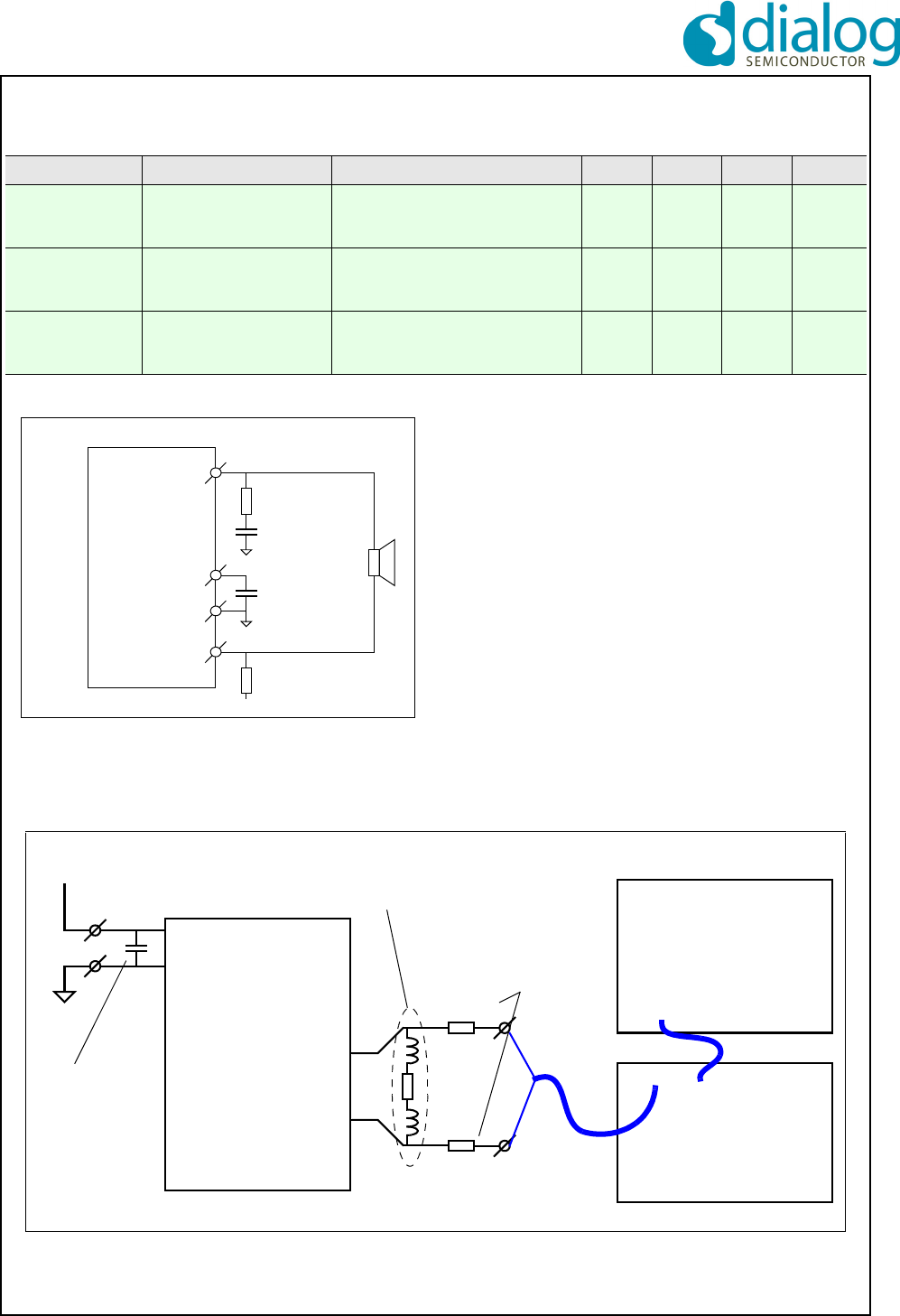
Table 13: VREFp load circuit
PARAMETER DESCRIPTION CONDITIONS MIN TYP MAX UNIT
Cload_vrefp VREFp (parasitic) load
capacitance
20 pF
Iout_vrefp VREFp output current 1mA
Figure 8 VREFp load circuit
Cload_vrefp
VREFp
VREFm
Iout_vrefp
Rout_vrefp
Table 14: LSRp/LSRn outputs
PARAMETER DESCRIPTION CONDITIONS MIN TYP MAX UNIT
Vlsr_0dB_unt Untrimmed differen-
tial RMS output volt-
age between LSRp
and LSRn in audio
mode (0 dBm0 refer-
ence level)
0 dBm0 on CIN (Note 20),
LSRATT[2:0] = 001,
@ 1020 Hz Load circuit A (see
Figure 9, Table 15) with RL1=
, Cp1 or load circuit B (see
Figure 10) with RL2, Cp2 and
Cs2
Tolerance:
• 13% when untrimmed
(BANDGAP_REG=8)
• 6% when trimmed
(Note 18)
621 714 807 mV
Rout_lsr Resistance of acti-
vated loudspeaker
amplifier outputs
LSRp and LSRn
1
Vlsr_dc DC offset between
LSRp and LSRn
(Note 8)
LSRATT[2:0] = 3
RL1 = 28
3 sigma deviation limits
-20 20 mV
SC14SPNODE SF DECT Module with integrated Antenna and FLASH
© 2012 Dialog Semiconductor B.V. 17 Jul 1, 2014 v1.6
Note 21: Clipping of the outputs occurs when the VDDPA drops and the following conditions becomes true. If CLASSD_CTRL_REG[CLASSD_CLIP]
is not equal to zero then upon a programmable number of clipping occurrences a CLASSD_INT is generated:
The software can stop clipping by reducing the gain via the GENDSP:
Clipping occurs if
Table 15: LSRp/LSRn load circuits
PARAMETER DESCRIPTION CONDITIONS MIN TYP MAX UNIT
Cp1_Rl1_inf Load capacitance see Figure 9, RL1 = 30 pF
Cp1_Rl1_1k Load capacitance see Figure 9, RL1 1 k100 pF
Rl1 Load resistance 28
Cp2 Parallel load
capacitance
see Figure 10 30 pF
Cs2 Serial load capacitance 30 F
Rl2 Load resistance 600
Figure 9 Load circuit A: Dynamic loudspeaker
RL1 Cp1
LSRp
LSRn
Figure 10 Load circuit B: Piezo loudspeaker
Cs2
LSRp
LSRn
RL2
Cp2
Table 16: PAOUTp, PAOUTn outputs
PARAMETER DESCRIPTION CONDITIONS MIN TYP MAX UNIT
Vpa_4v Differential rms output
voltage between
PAOUTp and PAOUTn
Trimmed bandgap
input = 0 dBm0, 1 kHz
(Note 17)
Output low-pass filtered
CLASSD_VOUT = 0
0.985 Vrms
Vpa_6v As above
CLASSD_VOUT = 1
1.478 Vrms
Zload_pa_4v Speaker impedance,
connected between
PAOUTp and PAOUTn
With these values, the peak cur-
rents stays within the operating
range.
4
Zload_pa_6v 6
Table 17: PAOUTp, PAOUTn outputs (Note 21)
PARAMETER DESCRIPTION CONDITIONS MIN TYP MAX UNIT
Rout_pa Differential output
resistance between
PAOUTp and PAOUTn
See (Note 21) 1
peak LowPassFiltered PAOUTp PAOUTm–
VDDPA VSSPA–
-----------------------------------------------------------------------------------------------------------------------Zload
Zload Rout_pa+
-------------------------------------------
SC14SPNODE SF DECT Module with integrated Antenna and FLASH
© 2012 Dialog Semiconductor B.V. 18 Jul 1, 2014 v1.6
Efficiency 75% at 300 mW@2 V, 500 mW@2.5 V into a 4 transducer.
Table 18: PAOUTp, PAOUTn external components
PARAMETER DESCRIPTION CONDITIONS MIN TYP MAX UNIT
C_VDDPA Decoupling capacitor on
VDDPA
Required when Class-D is used
and guaranteed life time.
(see Figure 11)
1F
Cs_PAOUT Snubber capacitor (to
reduce ringing at
PAOUTp/n)
Required when Class-D is used
to prevent EMI and guaranteed
life time. (see Figure 11)
1nF
Rs_PAOUT Snubber resistor (to
reduce ringing at
PAOUTp/n)
Required when Class-D is used
to prevent EMI and guaranteed
life time. (see Figure 11)
1
Figure 11 Class-D external components
PAOUTp
PAOUTn
VDDPA
VSS/GND
C_VDDPA
Cs_PAOUT
Rs_PAOUT
Rs_PAOUT
Figure 12 CLASS-D amplifier measurement setup
in out
in
AP-system2, settings:
15 H
15H
4
PAOUTp
PAOUTn
VDDPA
GND (2x)
dummy load
1 F ceramic
2.5 V (= VBAT)
DUT 100
100
(models typical speaker)
bw = <10 Hz until 30 kHz
filter = A-weighting
detection = 4/s RMS
input = high-ohmic
AP AUX-0025
passive switching ampli-
fier measurement filter
resistors reduce
influence from
measurement on
DUT
SC14SPNODE SF DECT Module with integrated Antenna and FLASH
© 2012 Dialog Semiconductor B.V. 19 Jul 1, 2014 v1.6
3.8 BATTERY MANAGEMENT
3.9 BASEBAND PART
Table 19: CHARGE_CTRL pin
PARAMETER DESCRIPTION CONDITIONS MIN TYP MAX UNIT
Voh_charge_ctrl Drive capability of pin
CHARGE_CTRL
sourcing 500 A1.6 V
Vol_charge_ctrl sinking 100 A0.2 V
Table 20: State of charge circuit (SoC) (Operating condition)
PARAMETER DESCRIPTION CONDITIONS MIN TYP MAX UNIT
Vsocp_socn Input voltage
between SOCp and
SOCn
With the prescribed 0.1 sense
resistor this results in the usable cur-
rent range
-100 +100 mV
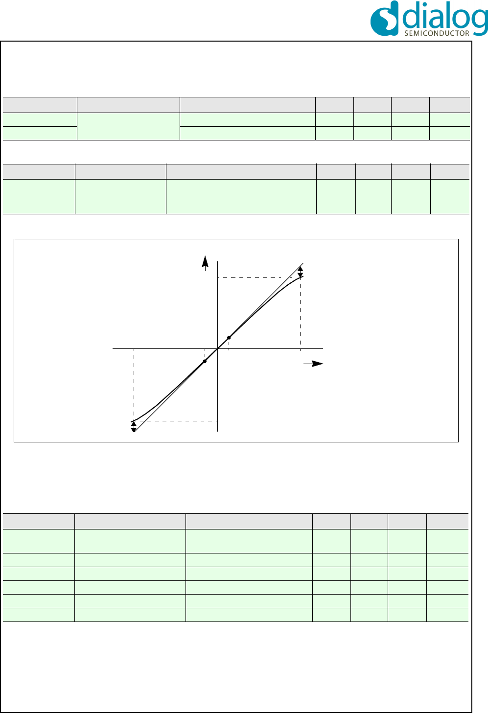
Figure 13 State of charge (SOC) counter accuracy
SoC_asym_err
input current
Counter ticks/s
1000 mA
100 mA
-100 mA
-1000 mA
100 mA extrapolation
A
BSoC_sym_err: A - |B|
Table 21: Baseband specifications
PARAMETER DESCRIPTION CONDITIONS MIN TYP MAX UNIT
Fbit_uart Serial interface bit rate UART; Interface for external
microprocessor or PC
115.2 kbit/s
Fbit_flash Flash download bit rate Via UART 115.2 kbit/s
Ibat_stdby_fp Standby supply current FP application (3.3 V) 55 60 mA
Ibat_act_fp Active supply current FP application (3.3 V) 65 70 mA
Ibat_stdby_pp Standby supply current PP application (3.3 V) 4.5 6mA
Ibat_act_pp Active supply current PP application (3.3 V) 30 40 mA
SC14SPNODE SF DECT Module with integrated Antenna and FLASH
© 2012 Dialog Semiconductor B.V. 20 Jul 1, 2014 v1.6
3.10 RADIO (RF) PART
Standards compliancy: ETS 301 406 (former TBR6).
Table 22: Radio specifications
PARAMETER DESCRIPTION CONDITIONS MIN TYP MAX UNIT
P_Rx Receiver sensitivity BER = 0.001; TA = 25 °C -93 -92 -89 dBm
P_Rx_T Receiver sensitivity, full
temperature range
BER = 0.001;
-40 °C TA 85 °C
-94 -87 dBm
IPL Intermodulation perform-
ance level (EN 301 406
section 4.5.7.6)
TA = 25 °C;
Pw = -80 dBm;
f = 2 channels
-35 dBm
NTP Normal transmitted power DECT: 250 mW 24 26 dBm
J-DECT: 10 mW average per
frame for each slot
23 24.5 dBm
DECT6.0: 100 mW (max
peak)
20.0 dBm
dPrfpa_T RFPA power variation, full
temperature range
-40 °C TA +85 °C 2.5 4dB
Fbit Bit rate GFSK modulation 1.152 Mbit/s
BW_Tx Transmitter bandwidth DECT GFSK;
NTP = 20 dB
1.728 MHz
Table 23: RFPA preferred settings for various power modes (PP application)
Address
(VES) Register / Parameter HPM/U
(USA)
HPM
(Europe)
HPM/J
(Japan)
0x3D RF_BBADC_CTRL_REG 0x0380 0x03A0 0x0398
0x39 RF_PA_CTRL1_REG 0x09A0 0x0CF0 0x2CE0
0x3B RF_TEST_MODE2_REG 0x0056 0x0062 0x0068
0x05 RF_PLL_CTRL2_REG[MODINDEX] 0x25 0x25 0x23
0x23 Upper RSSI threshold 0x2C N/A 0x28
0x24 Lower RSSI threshold 0x22 N/A 0x1E
SC14SPNODE SF DECT Module with integrated Antenna and FLASH
© 2012 Dialog Semiconductor B.V. 21 Jul 1, 2014 v1.6
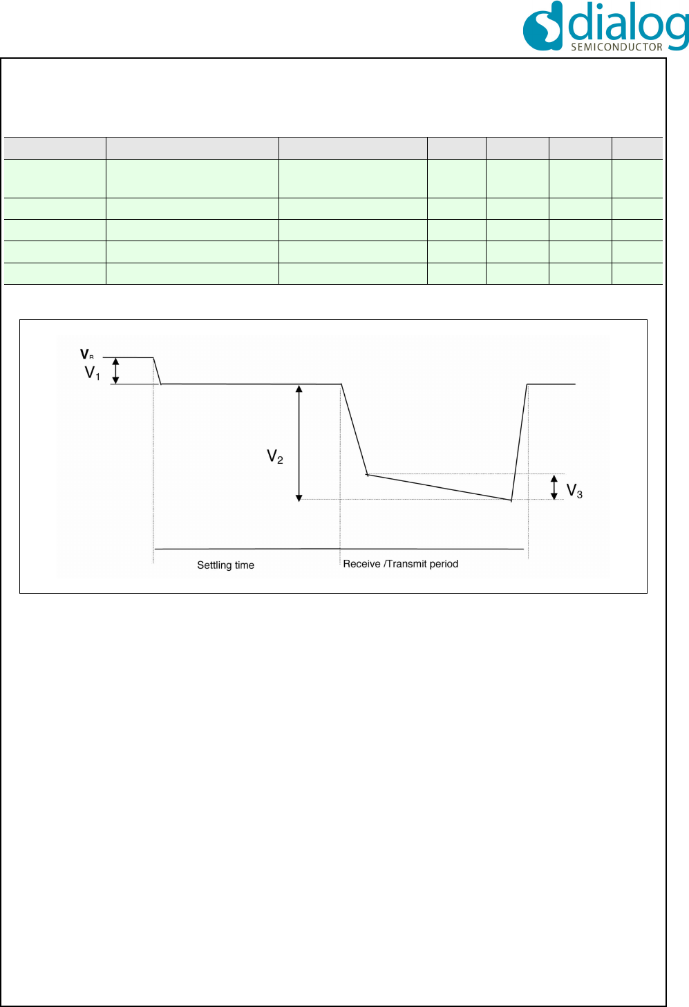
3.11 RF POWER SUPPLY
Table 24: Requirements for linear supply regulator
PARAMETER DESCRIPTION CONDITIONS MIN TYP MAX UNIT
VBAT IN Voltage at VBAT SW Unloaded VB
Loaded VB-V1-V2-V3
2.1 33.45 V
V1Settling time I = 50 mA 20 mV
V2Receive period I = 130 mA 100 mV
V2Transmit period I = 550 mA 200 mV
V3Drop during transmit 25 mV
Figure 14 RF power supply
B
SC14SPNODE SF DECT Module with integrated Antenna and FLASH
© 2012 Dialog Semiconductor B.V. 22 Jul 1, 2014 v1.6
3.12 RF CHANNEL FREQUENCIES
RF setting values must be followed according to
AN-D-204 when DECT country mode was changed.
Table 25: RF frequencies and channel numbers
Frequency
(MHz)
DECT
CH
J-DECT
CH
DECT6.0
CH
1881.792 9
1883.520 8
1885.248 7
1886.976 6
1888.704 5
1890.432 4
1892.160 3
1893.888 2
1895.616 1 1
1897.344 0 0
1899.072 10
1900.800 11
1902.528 12
1921.536 4
1923.264 3
1924.992 2
1926.720 1
1928.448 0
SC14SPNODE SF DECT Module with integrated Antenna and FLASH
© 2012 Dialog Semiconductor B.V. 23 Jul 1, 2014 v1.6
4.0 Design guidelines
4.1 PCB DESIGN GUIDELINES
• Because of the presence of the digital radio fre-
quency burst with 100 Hz time division periods (TDD
noise), supply ripple and RF radiation, special atten-
tion is needed for the power supply and ground PCB
layout.
• Power supply considerations
Both high and low frequency bypassing of the supply
line connections should be provided and placed as
close as possible to the SC14SPNODE. In order to
get the best overall performance for both FP and PP
applications, a number of considerations for the PCB
has to be taken into account.
• Make angle breaks on long supply lines to avoid
resonances at DECT frequencies. Maximum
80 mm before an angle break is recommended.
• Supply lines should be placed as far as possible
away from sensitive audio circuits. If it is neces-
sary to cross supply lines and audio lines, it
should be done with right angles between supply
and audio lines/circuits (microphone, ear-speaker,
speakerphone, etc.)
• Ground plane considerations
In order to achieve the best audio performance
and to avoid the influence of power supply noise,
RF radiation, TDD noise and other noise sources,
it is important that the audio circuits on both FP
and PP applications boards are connected to the
VREFM pin on the SC14SPNODE with separate
nets in the layout.
It is advised to provide the following audio circuits
with separate ground nets connected to the
VREFM pin:
• Microphone(s)
• Headset microphone and speaker
• Speakerphone (signal grounds)
Depending on the layout it may also be necessary to
bypass a number of the audio signals listed above to
avoid humming, noise from RF radiation and TDD
noise. It is also important to choose a microphone of
appropriate quality with a high RF immunity (with built-
in capacitor).
• ESD performance
Besides TDD noise, the ESD performance is impor-
tant for the end-application. In order to achieve a
high ESD performance supply lines should be
placed with a large distance from charging terminals,
display, headset connector and other electrical ter-
minals with direct contact to the ESD source.
On a two-layer PCB application it is important to
keep a simulated one layer ground. With a stable
ground ESD and TDD noise performance will always
improve.
• Clearance around test patterns
Pin number 81 to 88 are used for production test
purposes. In order to avoid any interference or dis-
turbance the area around these signal pins must be
kept clear of any signal and/or GND. The recom-
mended clearance is at least 1 mm as shown in Fig-
ure 15.
Figure 15 Clearance around test patterns
Test
pattern
0.9mm
0.6mm1.0mm
1.0mm
GND Pattern
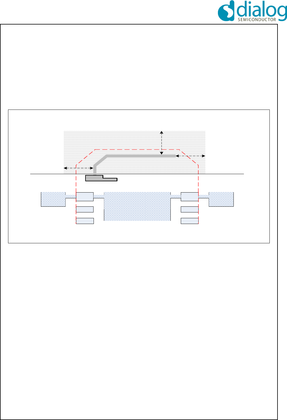
SC14SPNODE SF DECT Module with integrated Antenna and FLASH
© 2012 Dialog Semiconductor B.V. 24 Jul 1, 2014 v1.6
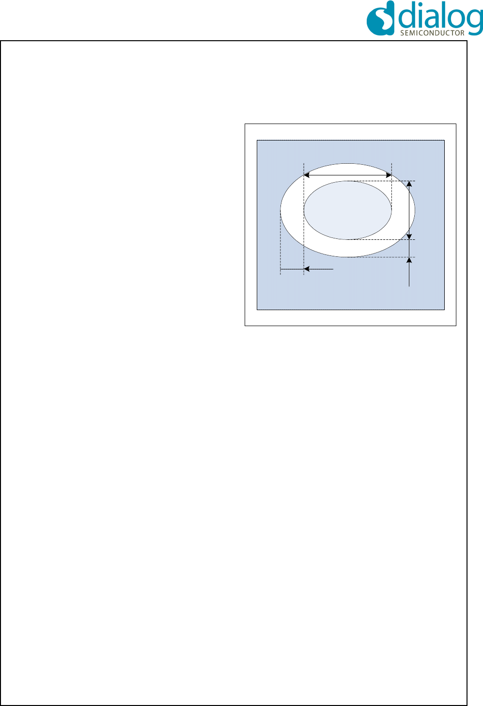
4.2 MODULE PLACEMENT ON THE MAIN BOARD
In order to ensure FCC compliance, proper coverage
and to avoid detuning of the antennas, it is required to
place the module on the main board free from other
surrounding materials.
Keep a distance of at least 10 mm from the antenna
elements to conducting objects and at least 5 mm to
non-conducting objects.
Keep in mind that electrical shielding objects, even
partly surrounding the antennas, will normally cause a
significant degradation of the coverage.
Place the module at the edge of the main-board as
shown in Figure 16.
If the module has to be placed away from the edge of
the main-board, then avoid conducting areas in front of
the antennas and make a cut-out in the main board
underneath the antennas as shown in the figure.
See Figure 18 and Figure 21 for the detailed package
outline.
4.3 PATTERN FOR PIN 79 ON THE MAIN BOARD
The copper pattern for pin 79 on the main board is very
important because it is part of the internal antenna of
the module. It is used to extend the internal antenna for
optimum RF performance.
The PCB pattern shown in Figure 19 under “pads C”
for pin 79 on the main board was used during module
certification.
4.4 PRECAUTIONS REGARDING UNINTENDED
COUPLING
The SC14SPNODE includes an internal antenna, so by
integration on the main board precautions shall be
taken in order to avoid any kind of coupling from the
main board to the RF part of the module.
If there is any doubt about this, a brief radio test should
be performed.
Figure 16 Module placement on the main board (top view)
178
No PCB area
2
376
77
GND
GND GND
79 Main boardModule
antenna extension
> 10 mm
> 10 mm
> 10 mm

SC14SPNODE SF DECT Module with integrated Antenna and FLASH
© 2012 Dialog Semiconductor B.V. 25 Jul 1, 2014 v1.6
5.0 Notices to OEM
The end product has to be certified again if it has
been programmed with other software than Dialog
standard software stack for portable part and/or
uses one or two external antenna(s).
5.1 FCC REQUIREMENTS REGARDING THE END
PRODUCT AND THE END USER
The end product that the module is integrated into must
be marked as follows:
“Contains Transmitter Module FCC ID: Y82-SC14S /
IC: 9576A-SC14S”
The literature provided to the end user must include the
following wording:
FCC compliance statement
This device complies with Part 15 of the FCC Rules.]
for only portable part.
Operation is subject to the following two conditions:
(1) this device may not cause harmful interference, and
(2) this device must accept any interference received,
including interference that may cause undesired opera-
tion of the device.
Module transmetteur ID IC: 9576A-SC14S.
Son fonctionnement est soumis aux deux conditions
suivantes: (1) cet appareil ne doit pas causer d’interfé-
rences nuisibles et (2) appareil doit accepter toute
interférence reçue, y compris les interférences qui peu-
vent perturber le fonctionnement.
Changes or modifications to the equipment not
expressly approved by the Party responsible for com-
pliance could void the user's authority to operate the
equipment.
NOTE: This equipment has been tested and found to
comply with the limits for a Class B digital device, pur-
suant to Part 15 of the FCC Rules. These limits are
designed to provide reasonable protection against
harmful interference in a residential installation.
This equipment generate, uses and can radiate radio
frequency energy and, if not installed and used in
accordance with the instructions, may cause harmful
interference to radio communications. However, there
is no guarantee that interference will not occur in a par-
ticular installation.
If this equipment does cause harmful interference to
radio or television reception, which can be determined
by turning the equipment off and on, the user is
encouraged to try to correct the interference by one or
more of the following measures:
• Reorient or relocate the receiving antenna
• Increase the separation between the equipment and
receiver
• Connect the equipment into an outlet on a circuit dif-
ferent from that to which the receiver is connected.
• Consult the dealer or an experienced radio/TV tech-
nician for help.
Privacy of communications may not be ensured when
using this phone.
5.2 INDUSRY CANADA REQUIREMENTS REGARD-
ING THE END PRODUCT AND THE END USER
The host device shall be properly labelled to identify
the modules within the host device. The Industry Can-
ada certification label of a module shall be clearly visi-
ble at all times when installed in the host device,
otherwise the host device must be labelled to display
the Industry Canada certification number of the mod-
ule, preceded by the words "Contains transmitter mod-
ule", or the word "Contains", or similar wording
expressing the same meaning, as follows:
Contains transmitter module IC: 9576A-SC14S
L'appareil hôte doit être étiqueté comme il faut pour
permettre l'identification des modules qui s'y trouvent.
L'étiquette de certification d'Industrie Canada d'un
module donné doit être posée sur l'appareil hôte à un
endroit bien en vue en tout temps. En l'absence d'éti-
quette, l'appareil hôte doit porter une etiquette donnant
le numéro de certification du module d'Industrie Can-
ada, précédé des mots " Contient un module d'émis-
sion ", du mot " Contient " ou d'une formulation
similaire exprimant le même sens, comme suit :
Contient le module d'émission IC: 9576A-SC14S
This device complies with Industry Canada licence-
exempt RSS standard(s). Operation is subject to the
following two conditions: (1) this device may not cause
interference, and (2) this device must accept any inter-
ference, including interference that may cause unde-
sired operation of the device.
Le présent appareil est conforme aux CNR d'Industrie
Canada applicables aux appareils radio exempts de
licence. L'exploitation est autorisée aux deux condi-
tions suivantes : (1) l'appareil ne doit pas produire de
brouillage, et (2) l'utilisateur de l'appareil doit accepter
tout brouillage radioélectrique subi, même si le brouil-
lage est susceptible d'en compromettre le fonctionne-
ment.
CAN ICES-3 (B)/NMB-3(B)

SC14SPNODE SF DECT Module with integrated Antenna and FLASH
© 2012 Dialog Semiconductor B.V. 26 Jul 1, 2014 v1.6
5.3 PRECAUTIONS REGARDING UNINTENDED
COUPLING
Integration on the main board precautions shall be
taken in order to avoid any kind of coupling from the
main board to the RF part of the module. If there is any
doubt about this, a radio short test should be per-
formed.
5.4 END APPLICATION APPROVAL
The module is intended to be used in an end applica-
tion. Type approval concerning the end product, except
for the module, should off cause be done. Please con-
tact a test-house in order to clarify what is needed.
5.5 SAFETY REQUIREMENTS
This section provides of an overview of the safety
requirements you must adhere to when working with
the SC14SPNODE.
• The specific external power supply for the
SC14SPNODE has to fulfil the requirements accord-
ing to clause 2.5 (Limited power source) of this
standard EN 60950-1:2006.
• Interconnection circuits shall be selected to provide
continued conformance to the requirements of
clause 2.2 for SELV (Safety Extra Low Voltage) cir-
cuits according to EN 60950-1:2006 after making
connections.
• Interface type not subjected to over voltages (i.e.
does not leave the building).
• Requirements additional to those specified in this
standard may be necessary for:
• Equipment intended for operation in special envi-
ronments (for example, extremes of temperature,
excessive dust, moisture or vibration, flammable
gases and corrosive or explosive atmospheres).
• Equipment intended to be used in vehicles, on
Board ships or aircraft, in tropical countries or at
altitudes greater than 2000 m.
• Equipment intended for use where ingress of
water is possible.
• Installation by qualified personnel only!
• The product is a component intended for installation
and use in complete equipment. The final accept-
ance of the component is dependent upon its instal-
lation and use in complete equipment.
SC14SPNODE SF DECT Module with integrated Antenna and FLASH
© 2012 Dialog Semiconductor B.V. 27 Jul 1, 2014 v1.6
6.0 Package information
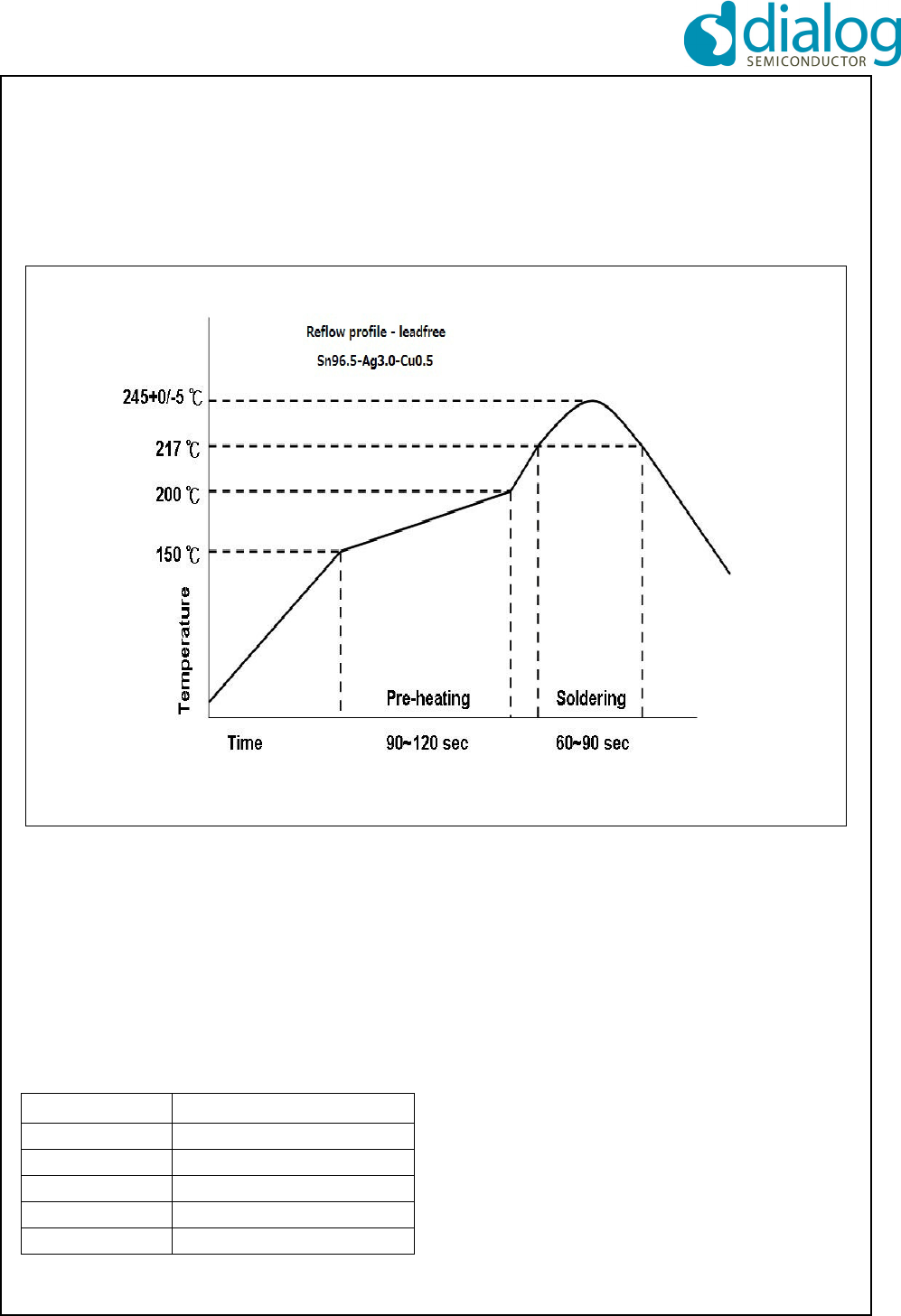
6.1 SOLDERING PROFILE
The SC14SPNODE should be soldered using a stand-
ard reflow soldering profile and lead free solder paste
as shown below. Adjustments to the profile may be
necessary depending on process requirements.
6.2 MOISTURE SENSITIVITY LEVEL (MSL)
The MSL is an indicator for the maximum allowable
time period (floor life time) in which a moisture sensi-
tive plastic device, once removed from the dry bag, can
be exposed to an environment with a maximum tem-
perature of 30°C and a maximum relative humidity of
60% RH. before the solder reflow process.
The SC14SPNODE is qualified to MSL 3.
Figure 17 Reflow profile
MSL Level Floor Life Time
MSL 4 72 hours
MSL 3 168 hours
MSL 2A 4 weeks
MSL 2 1 year
MSL 1 Unlimited at 30°C/85%RH
SC14SPNODE SF DECT Module with integrated Antenna and FLASH
© 2012 Dialog Semiconductor B.V. 28 Jul 1, 2014 v1.6
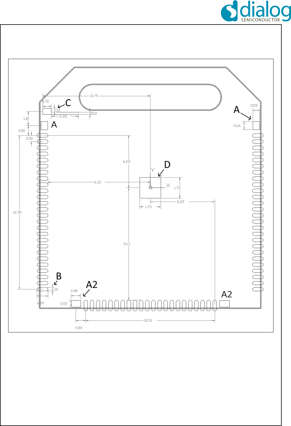
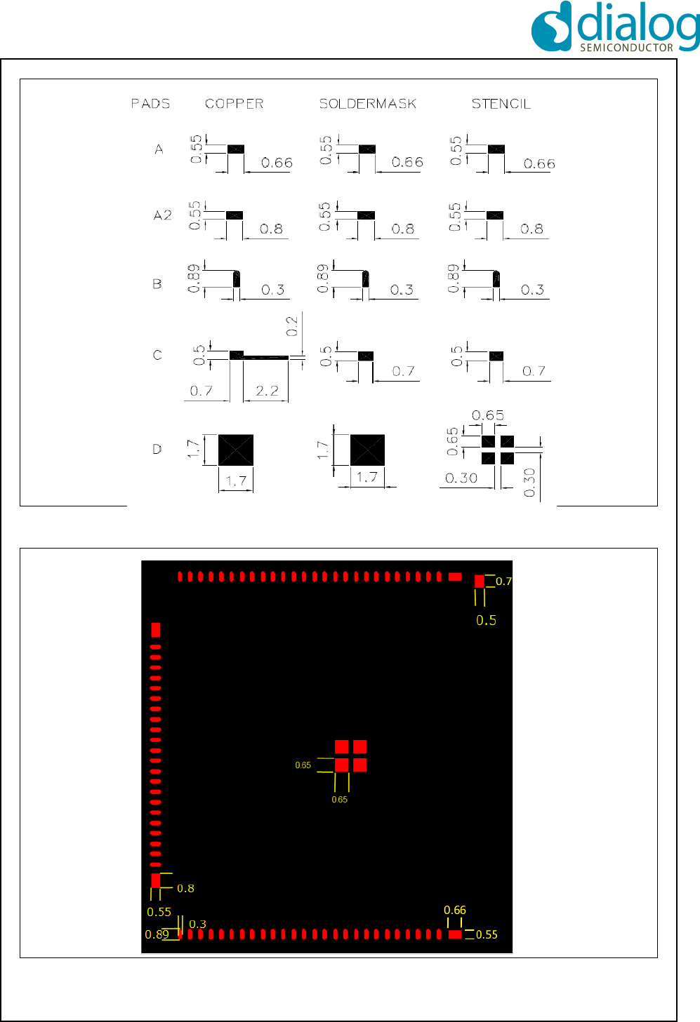
6.3 COPPER PAD, SOLDER OPENING AND STEN-
CIL
For the stencil a thickness of 0.122 mm is
recommended. Recommended copper pad, solder
mask opening and stencil are shown below.
Figure 18 Pad dimensions
SC14SPNODE SF DECT Module with integrated Antenna and FLASH
© 2012 Dialog Semiconductor B.V. 29 Jul 1, 2014 v1.6
Figure 19 Copper pad, Solder mask opening and Stencil
Figure 20 Solder stencil
SC14SPNODE SF DECT Module with integrated Antenna and FLASH
© 2012 Dialog Semiconductor B.V. 30 Jul 1, 2014 v1.6
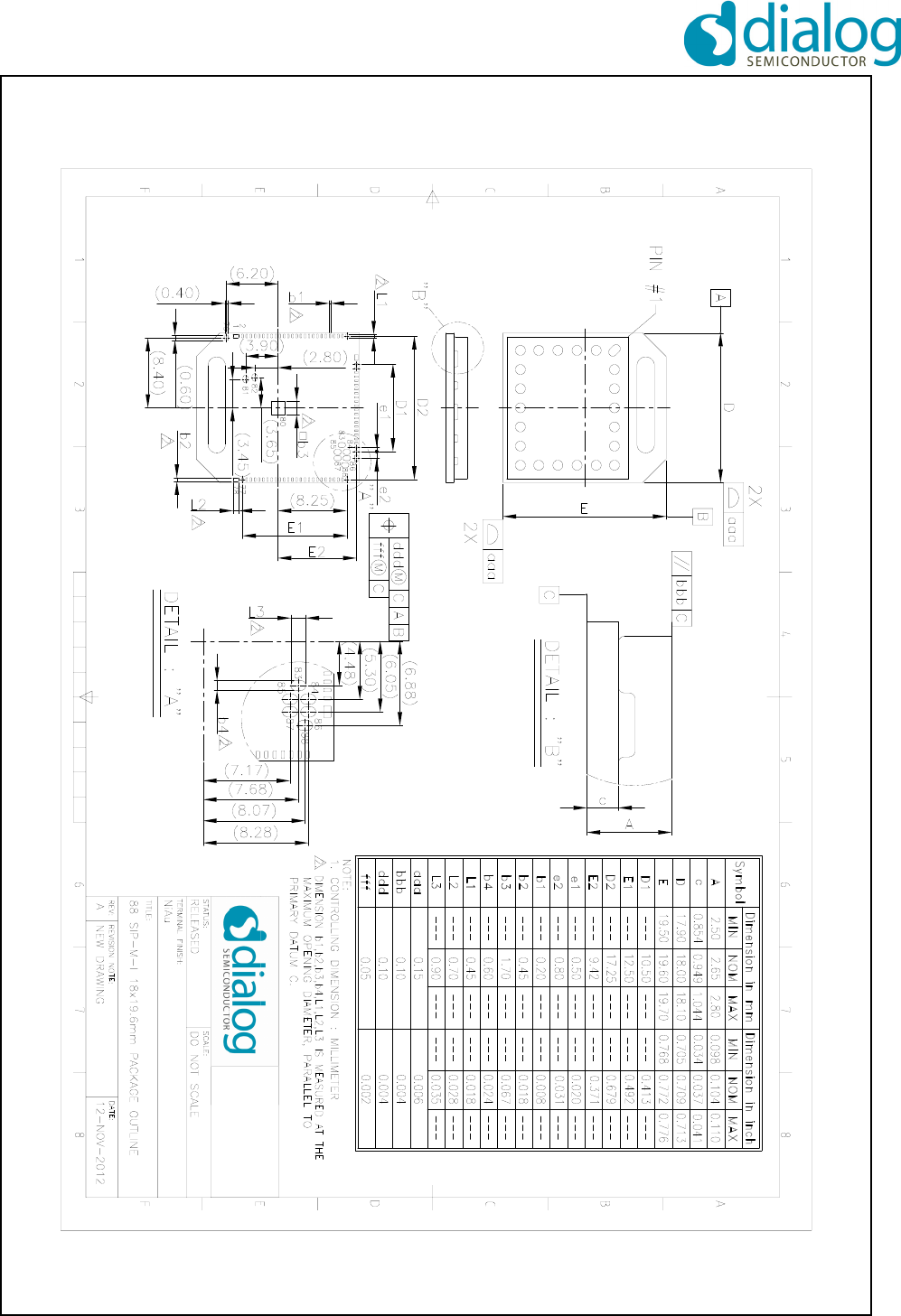
6.4 MECHANICAL DIMENSIONS
Figure 21 Package outline drawing

SC14SPNODE SF DECT Module with integrated Antenna and FLASH
© 2012 Dialog Semiconductor B.V. 31 Jul 1, 2014 v1.6
7.0 Revision history
Jul1, 2014 v1.6:
• Changed maximum RF output power for DECT 6.0
Apr 16, 2014 v1.5:
• Added an explanation for RF1 on 2.6
Feb 11, 2014 v1.4:
• Correct 6.3Copper pad, solder openinG and
STENCIL28
Feb 4, 2014 v1.3:
• Modified 6.3Copper pad, solder openinG and
STENCIL28
Nov 8, 2013 v1.2:
• Added section “5.2 INDUSTRY CANADA
REQUIREMENTS REGARDING THE END PROD-
UCT AND THE END USER”
Sept 12, 2013 v1.1:
• Ordering code for tray version corrected.
• Ordering code for tape-on-reel version removed.
July 10, 2013 v1.0: Initial version

SC14SPNODE SF DECT Module with integrated Antenna and FLASH
© 2012 Dialog Semiconductor B.V. 32 Jul 1, 2014 v1.6
Product Status Definitions
Dialog Semiconductor reserves the right to make changes without notice to any products herein to improve reliabil-
ity, function or design. Dialog Semiconductor does not assume any liability arising out of the application or use of
any product or circuit described herein; neither does it convey any license under its patent rights, nor the right of oth-
ers.
Datasheet Status Product Status Definition
Advance Information Formative or in Design This data sheet contains the design specifications for prod-
uct development. Specifications may change in any manner
without notice.
Preliminary First Production This data sheet contains preliminary data. Supplementary
data will be published at a later date. Dialog Semiconductor
reserves the right to make changes at any time without
notice in order to improve design and supply the best possi-
ble product.
No Identification Noted Full production This data sheet contains final specifications. Dialog Semi-
conductor reserves the right to make changes at any time
without notice in order to improve design and supply the best
possible product.
Obsolete Not in Production This data sheet contains specifications on a product that has
been discontinued by Dialog Semiconductor. The data-sheet
is printed for reference information only.
Life Support Policy
DIALOG’S PRODUCTS ARE NOT AUTHORIZED FOR USE AS CRITICAL COMPONENTS IN LIFE SUPPORT
DEVICES OR SYSTEMS WITHOUT THE EXPRESS WRITTEN APPROVAL OF THE PRESIDENT AND GENERAL
COUNCIL OF DIALOG SEMICONDUCTOR. As used herein:
1. Life support devices or systems are devices or
systems which,
(a) are intended for surgical implant into the
body, or (b) support or sustain life, and whose
failure to perform, when properly used in accord-
ance with instructions for use provided in the
labelling, can be reasonably expected to result
in a significant injury to the user.
2. A critical component is any component of a life
support device or system whose failure to per-
form can be reasonably expected to cause the
failure of the life support device or system, or to
affect its safety or effectiveness.
Germany Headquarters
Dialog Semiconductor GmbH
Phone: +49 7021 805-0
United Kingdom
Dialog Semiconductor (UK) Ltd
Phone: +44 1793 757700
The Netherlands
Dialog Semiconductor B.V.
Phone: +31 73 640 88 22
Dialog Semiconductor does not assume any responsibility for use of any circuit described, no circuit patent licenses are implied, and Dialog
reserves the right, at any time without notice, to change said circuitry or specifications.
Contacting Dialog Semiconductor
RoHS Compliance
Dialog Semiconductor complies to European Directive 2001/95/EC and from 2 January 2013 onwards to European
Directive 2011/65/EU concerning Restriction of Hazardous Substances (RoHS/RoHS2).
Dialog Semiconductor’s statement on RoHS can be found on the customer portal http:/portal.dialog-semiconduc-
tor.com. RoHS certificates from our suppliers are available on request.
North America
Dialog Semiconductor Inc.
Phone: +1 408 727 3200
Japan
Dialog Semiconductor K. K.
Phone: +81 3 5425 4567
Taiwan
Dialog Semiconductor Taiwan
Phone: +886 226 580 388
Singapore
Dialog Semiconductor Singapore
Phone: +65 64845419
China
Dialog Semiconductor China
Phone: +852 2607 4271
Korea
Dialog Semiconductor Korea
Phone: +82 2 569 2301