E F Johnson 2425110 242-5110 User Manual 011402 revised 1 Pages 86 to 113 operators manual
E. F. Johnson Company 242-5110 011402 revised 1 Pages 86 to 113 operators manual
Contents
- 1. Operating Manual
- 2. 011402 revised 1 Pages 1 to 57 operators manual
- 3. 011402 revised 1 Pages 57 to 85 operators manual
- 4. 011402 revised 1 Pages 86 to 113 operators manual
- 5. Manual
011402 revised 1 Pages 86 to 113 operators manual

CIRCUIT DESCRIPTION
4-11 September 2001
Part No. 001-5100-001
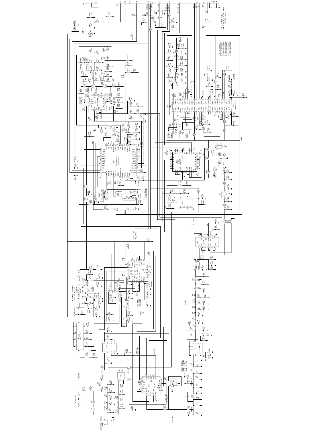
4.4.6 UART
The UART performs parallel to serial and serial
to parallel conversion. The serial format used is a 9-bit
format with start and stop bits. The serial transmission
speed is 19200 bps. The UART appears as eight regis-
ters visible in the I/O space of the DSP starting at
every multiple of 0008h from 0000h to 07FFh. U11
performs the address decoding by selecting the UART
when both IS* and A15 are low. Crystal Y2 along with
the internal oscillator of the UART provides the clock
required to generate the correct bit rate on the serial
output of the UART.
When the UART receives a new serial word or is
ready to accept a new word to send from the DSP, it
generates an interrupt on INTRN. This pin is
connected to one of the hardware interrupt lines on the
DSP. The DSP responds by reading the status register
in the UART and by answering accordingly.
4.4.7 ADSIC
The ADSIC is a complex custom IC which
performs many analog-to-digital, digital-to-analog,
and purely digital functions as previously described.
The ADSIC has four internal registers accessible by
the DSP. They are selected through the use of address
lines A15, A14, A13, A2, A1, A0, IS* (IS* needs to be
inverted with U4 to be compatible with the logic level
required by the ADSIC), RD*, and WR*. Two of these
registers are read-only while the two others are write-
only. Therefore, they can be accessed as two locations
in the I/O spaces. Due to the decoding performed,
those locations appear at the following addresses:
Fxx0h, Fxx1h, Fxx8h, Fxx9h, Exx0h, Exx1h, Exx8h,
and Exx9h.
Crystal Y1 along with the internal oscillator in
the ADSIC provide a 20 MHz clock. This clock signal
is used internally by the ADSIC and is also multiplied
by two to provide a 40 MHz clock to the DSP. The
frequency of the clock can be electronically shifted a
small amount by controlling varicap D1 through the
OSCW pin (U3-97). This removes interference created
on some channels by the clock.
The ADSIC and DSP exchange the sampled
receive data and the sampled VCO modulation signal
through a serial port. This serial port consists of pins
SCKR*, RFS, RxD, TxD, SCKT, and TFS on the
ADSIC. U21 and U1 modify the relative phase of TxD
and TFS to be compatible with the timing required on
the serial port of the DSP.
SDO is the output of the internal speaker DAC.
MAI is the input of the internal microphone attenuator
and is followed by the microphone ADC.
The ADSIC is configured partially by the DSP
through its data and address bus (see preceding).
However, most of the configuring is provided through
an SPI compatible serial bus. This SPI serial bus
consists of pins SEL*, SPD, and SCLK. The other side
of this bus is connected to the controller on the
Keypad Board.
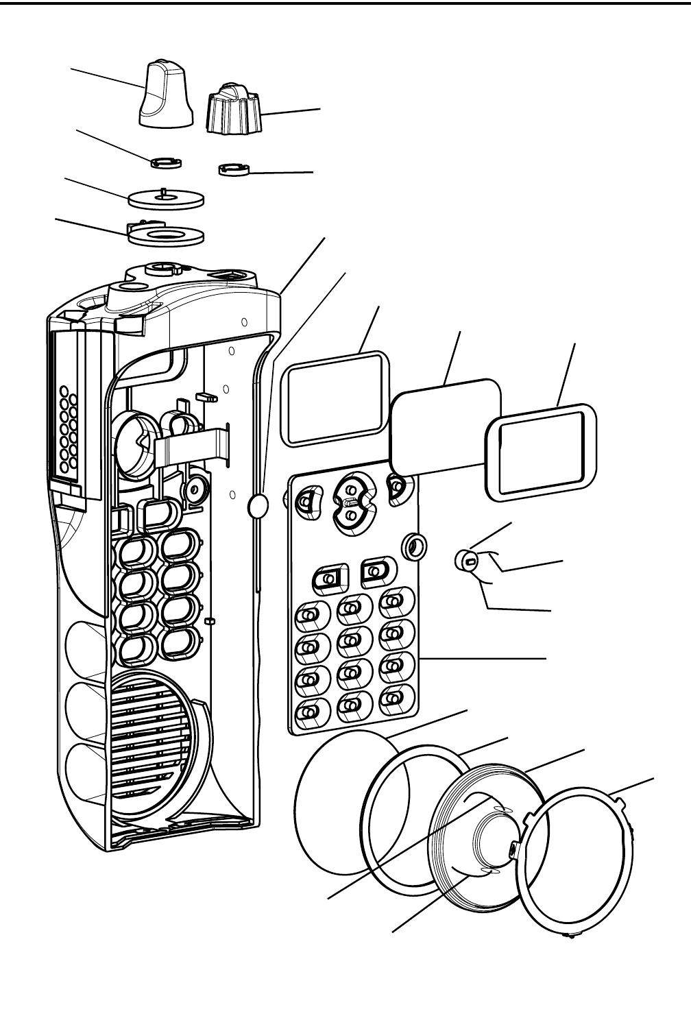
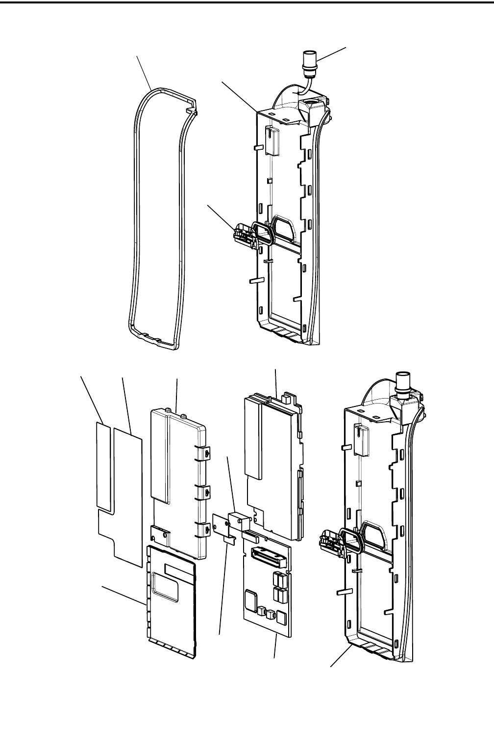
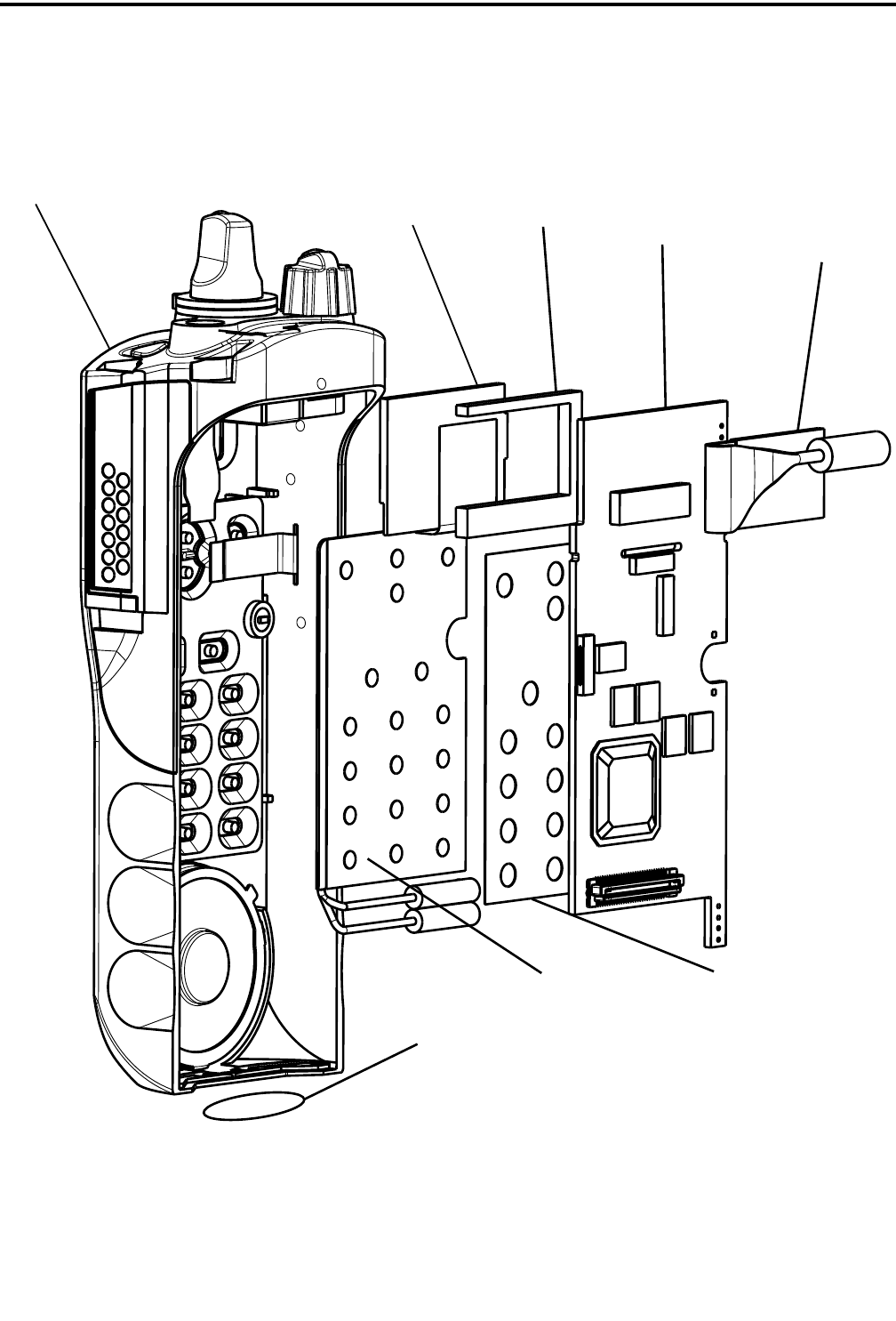
4.5 KEYPAD BOARD
4.5.1 INTRODUCTION
The Keypad Board contains a microcontroller,
LCD Display, Display Driver, Audio circuits, and
Power supply. The Keypad Board interfaces with the
Digital board via J4, with the Top Control rigid flex
circuit via J13, and with the side buttons, PTT switch,
and accessory connector through J5.
4.5.2 FUNCTIONAL DESCRIPTION
The microcontroller provides an interface
between the hardware and the DSP (on the Digital
Board). When the user presses or rotates a control such
as the channel selector switch, a side option or PTT
switch, or a keypad key, the microcontroller signals
the change to the DSP. Conversely, when the DSP
needs to change the display or an LED, it signals the
microcontroller which then performs the action. The
microcontroller also controls peripheral ICs such as
the synthesizer, reference oscillator, display, and
ADSIC.
The microcontroller uses a serial bus to commu-
nicate with the DSP and another RS232 bus to
communicate with the side port connector. The side
connector bus is used for external communication with
a computer running the programming or tuning soft-
ware. Finally, the microcontroller maintains certain
operating parameters in the associated EEPROM
which is controlled via a two-wire serial bus.
DIGITAL BOARD (CONT’D)

CIRCUIT DESCRIPTION
4-12 September 2001
Part No. 001-5100-001
4.5.3 MICROCONTROLLER
The microcontroller is a Motorola
M68HC08XL36 chip. It includes 28K bytes of internal
ROM memory and 1K byte of internal SRAM. It does
not have an external bus and therefore cannot access
any external program memory.
The clock to the microcontroller is provided by
Y1 and an internal oscillator. The frequency of the
clock can be slightly offset by polarizing the base of
Q3 through software control. This prevents RF inter-
ference on some channels caused by the clock.
The microcontroller contains an SPI-compatible
synchronous serial bus. This bus consists of pins
MISO (U1-53), MOSI (U1-52), SPSCK (U1-50), and
a chip enable for each device with which it communi-
cates. The devices which communicate with the
microcontroller through this bus are as follows:
•Top Display driver chip (Top Display board)
•Front Display driver chip (Digital board)
•ADSIC chip (Digital board)
•Reference Oscillator (RF Board)
•Front-End DAC (RF Board)
•Synthesizer chip (RF Board)
•Optional DES board.
The microcontroller communicates with the DSP
chip (Digital board) through a custom serial bus. This
serial port includes pins PTA3 (U1-8), PTA4 (U1-9),
PTA5 (U1-10), PTA6 (U1-11), and PTA7 (U1-12).
The microcontroller uses its SCI asynchronous
serial bus for external communication with a computer
running programming or tuning software. The SCI
pins RxD (U1-42) and TxD (U1-43) are connected to
RS232 driver receiver U5. The other signals of a stan-
dard RS232 computer port (DSR, DTR, CTS, RTS)
are generated using microcontroller input/outputs.
The RS232 driver U5 converts signals from a
logic level of 0 and 5 V to a logic level of –10 and
+10V. The chip contains an internal charge pump to
generate –10V and +10V from the 5V power supply.
The RS232 chip can be put in standby mode by
leaving the line K/F-RS232* floating. This line is
connected to the side connector which allows it to turn
on U5 only when a computer is connected to the radio.
The keypad interfaces with the microcontroller
through eight lines (4 rows x 4 columns). The micro-
controller regularly polls these lines to detect a key
closure.
Serial EEPROM U3 is used to store some impor-
tant radio parameters. The EEPROM is read to or
written from using I/O lines PTC6 and PTC7 of the
microcontroller. PTC6 is used for the Data line, and
PTC7 is used as a clock line.
Shift register U14 expands the number of I/O
lines of the microcontroller. It uses the same data and
clock as the EEPROM plus an additional line (U1-45)
to control the latch. Other user interface inputs such as
the PTT and toggle switches are directly connected to
an I/O line of the microcontroller.
4.5.4 LOW VOLTAGE DETECT
Voltage comparator U4 detects a low voltage
condition and communicates this information to the
microcontroller through the pin PTC5 (U1-30). The
microcontroller can also detect through I/O IRQ2*
(U1-62) that a battery is connected.
4.5.5 LCD DISPLAYS AND DISPLAY DRIVERS
The radio has two displays which each have eight
characters, several icons and a backlight. One display
is located on the Keypad Board while the other display
is located on the Top Display Board. Each display is
driven by its own driver. The drivers are programmed
by the microcontroller through the SPI bus. Both
display drivers are connected to the common PI bus
but are individually addressable so that the displays
may show different information at the same time.
4.5.6 AUDIO CIRCUITS
The audio circuits on the Keypad/Display Board
consist of four op amps, two audio power amplifiers,
and an analog switch.
In receive mode, the analog receive waveform
created by the ADSIC (on the Digital Board) is fed to
an op amp summing amplifier (U9B). This amplifier
sums in the audio tones that are generated by the
microcontroller. The output of the summing amplifier
KEYPAD BOARD (CONT’D)

CIRCUIT DESCRIPTION
4-13 September 2001
Part No. 001-5100-001
is then fed through the volume control potentiometer
to a second op amp buffer.
The buffer output is routed to a pair of audio
power amplifiers: one to drive the internal speaker and
another to drive the external speaker. Only one of
these audio power amplifiers can be active at a time.
The active power amplifier is selected by the OPT
SEL 1 line (J5-12). The MUTE line turns the active
power amplifier on or off by disconnecting the battery
voltage from the audio power amplifier IC using the
transistor Q4. Transistors Q8 and Q9 and their associ-
ated RC networks remove popping sounds from the
speaker audio by delaying the unmuting of the audio
amp compared to the unMUTE command.
In transmit mode, the audio for transmission can
be selected from either an internal or external micro-
phone, depending upon the presence of an external
microphone and which PTT is pressed. An analog
switch is used to route either the internal or external
microphone signal to the microphone amplifier. The
external microphone signal is buffered by an op amp.
The microphone amplifier has a gain of ten, and is
equipped with a pair of clipping diodes to prevent the
amplified microphone signal from over-driving the A/
D input on the ADSIC.
4.5.7 VOLTAGE REGULATION
The 5-Volt Digital Supply is produced by
switching DC-DC converter U12 which operates off
the Unswitched B+ Supply. The switching frequency
is around 160 kHz. A switching regulator is used to
improve efficiency since the 5-Volt Digital Supply
power consumption is a large percentage of the total
power consumption of the radio. The peak-to-peak
residual ripple on the 5-Volt Digital supply is approxi-
mately 50 mV.
The DC-DC converter is controlled by a wired
AND gate on the Shutdown pin of the device. The two
inputs of the wired AND gate are the SW_B+ and the
output PTC4 of the microcontroller U1. When either
input is high, the DC-DC converter is operating.
The DC-DC converter has a soft-start feature
(R98, C136) to prevent chattering of the output regu-
lated voltage due to “bouncing” of the on/off switch.
The converter has current limiting that limits output
current to 1.5 A. The under voltage protection turns
the converter off if the input (Unswitched B+) voltage
drops below 5.45 V.
The 5-Volt Analog Supply is produced by a linear
regulator running from the Unswitched B+ Supply.
The Unswitched B+ input to the regulator is switched
on and off by a FET that is turned on by the 5-Volt
Digital Supply. The peak-to-peak output ripple of the
5-Volt Analog regulator is less than 10 mV which is
appropriate for analog circuits.
4.6 TRANSMIT FREQUENCY
DETERMINATION
The operational frequency of the transmitter is
determined by the PLL (Phase-Locked-Loop)
consisting of synthesizer U204 and VCO circuit Q202/
U201. Reference oscillator U203 generates and
supplies a reference signal of 16.8 MHz to synthesizer.
The synthesizer contains a programmable reference
divider, programmable A and B dividers, a program-
mable prescaler counter (P), and a programmable frac-
tional N divider with two programmable values (N
numerator and N denominator).
All of these dividers are programmed through the
serial interface which connects the synthesizer to the
controller microprocessor. The 16.8 MHz reference
oscillator frequency is divided down to a synthesizer
reference frequency of 2.1, 2.4, or 2.225 MHz. This
signal is fed to the phase detector which generates the
steering voltage for the VCO. The output of the VCO
circuit is coupled back and divided by AP+B and then
divided by the fractional divider and fed into the
second input of the phase detector. The VCO buffer
has two outputs. One input goes to the input of Rx
mixer chip U2, and the other is applied to the input of
power amplifier module U105.
4.7 HARMONIC FILTER
The transmitter harmonic filter consists of C148-
C151, L126, L127, and L128.With VHF models only,
it also consists of C129 and C130. The circuit is essen-
tially a seven-pole low-pass filter. With VHF units
only, two additional poles are inserted by C129 and
C130 which are series resonant with L126 and L127.
KEYPAD BOARD (CONT’D)
5-1 September 2001
Part No. 001-5100-001
ALIGNMENT PROCEDURE
SECTION 5 ALIGNMENT PROCEDURE
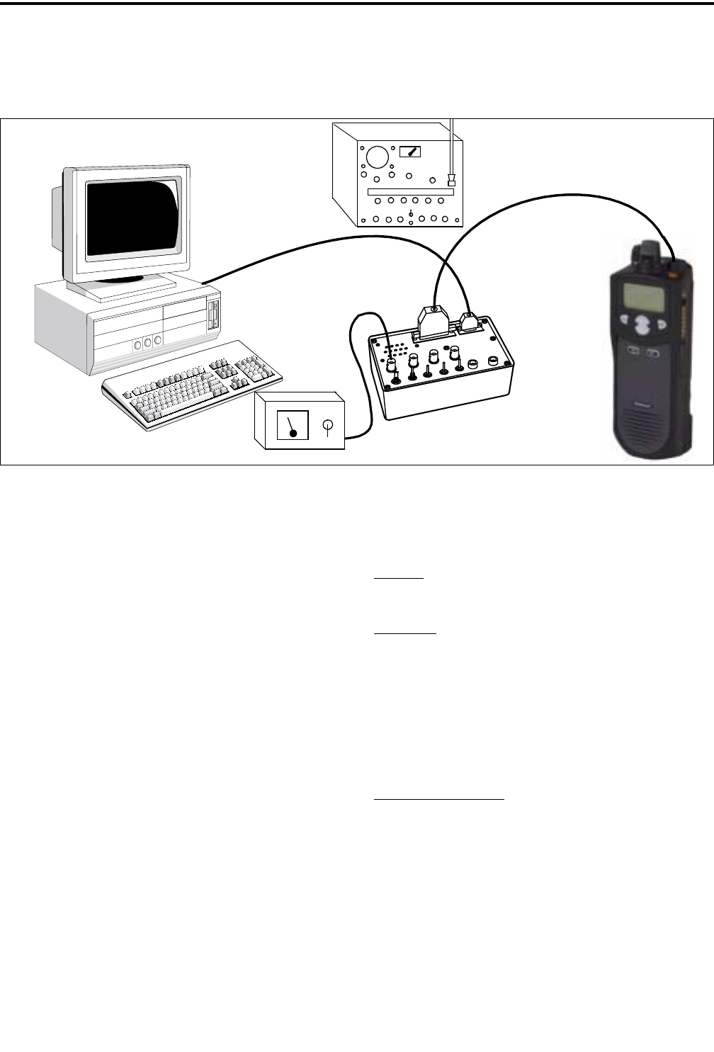
Figure 5-1 Alignment Setup
Communication
SINAD Meter
Monitor
5.1 GENERAL
5.1.1 INTRODUCTION
The following alignment procedure should be
performed if repairs are made that could affect the
factory alignment or if adjustments may have changed
for some other reason.
To perform transceiver alignment, a PC-compat-
ible computer, the programming interface cable, and
PCTune software are required (see Table 1-1). In addi-
tion, to adjust the squelch level, the Radio Interface
Box (RIB) and radio-to-RIB cable are required. The
programming setup is shown in Figure 5-1.
All adjustments are set digitally using the
computer. Therefore, there is no need to disassemble
the transceiver to access adjustment points. In addi-
tion, audio test signals are generated internally, so an
audio generator is not required. The required test
equipment is shown in Figure 5-1.
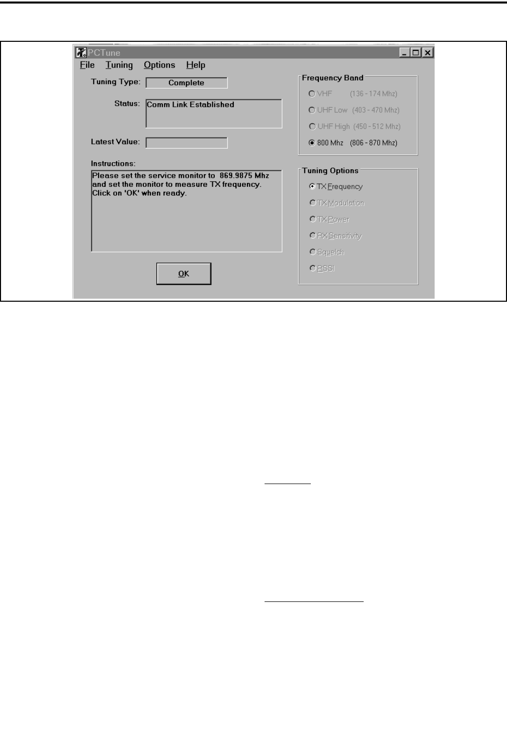
5.1.2 TUNE SOFTWARE
General
The PCTune software is a Windows® program.
Minimum software and hardware requirements are as
follows:
•Windows® 95, 98, or 3.1
•386SX or faster microprocessor
•4 megabytes of RAM
•3 megabytes free space available on hard drive.
•An available serial port
Software Installation
Proceed as follows to install this software:
1. Close all applications that are currently running
(other than Windows).
2. Insert the disk containing the PCTune software in
drive A: (or B:).

ALIGNMENT PROCEDURE
5-2 September 2001
Part No. 001-5100-001
3. From the Windows 95 taskbar, choose RUN and
open SETUP.EXE on drive A: (or B:). Alternatively,
use File Explorer and double click SETUP.EXE.
From the Windows 3.1 Program Manager, choose
FILE > RUN and select the SETUP.EXE file on
drive A: (or B:).
4. Follow the instructions on the screen. The program
is automatically loaded on the hard drive and start-
up shortcuts or groups are created.
Starting PCTune
From Windows 95 - Select Start in the taskbar, then
Programs > PCTune > PCTune x.x.x.
From Windows 3.1 - From the Program Manager,
open the PCTune group and then double click the
PCTune icon.
Exiting PCTune
Select FILE > EXIT or press ALT + F4.
On-Line Help
On-line help is not available at this time.
5.1.3 PRELIMINARY
1. With transceiver power turned off, connect the
female DB9 connector of the programming inter-
face cable to an unused serial port of the computer.
2. Connect the other end of the programming interface
cable to the accessory/programming jack on the side
of the transceiver.
3. Start the program as described in the preceding
section. Select Options > Set Com Port and make
sure that the correct serial port is selected (see
screen in Figure 5-2).
4. Turn transceiver power on and select Tuning >
Complete Tuning to automatically step through a
complete alignment or Partial Tuning to adjust only
certain settings or randomly select adjustments.
5. The computer then attempts to establish communi-
cation with the transceiver. A message is displayed
to indicate success or failure. From this point,
prompts are displayed for each step of the program-
ming procedure.
5.2 TRANSMIT FREQUENCY TUNING
The transmit frequency is set by transmitting on
the indicated frequency and then adjusting the refer-
ence oscillator frequency via the tuning software.
Proceed as follows:
1. Connect a 50-ohm load to the antenna jack and
monitor the transmit signal with a communication
monitor.
2. Set the communication monitor to the indicated
frequency and click OK to key the transmitter.
3. Adjust the frequency by clicking the + and – keys.
The current setting is indicated in the “Current
Value” box. When the frequency is correct, click
OK again to complete the adjustment and store the
setting.
5.3 TRANSMIT MODULATION TUNING
Transmit modulation is set by balancing the
modulation produced by 80 Hz and 3 kHz tones and
then setting modulation limiting using a 1 kHz tone.
All these tones are internally generated by the trans-
ceiver, so no external audio generator is required.
Proceed as follows:
1. Click OK with “TX Modulation” selected. Set the
communication monitor for the displayed
frequency.
2. Click OK to transmit a signal modulated with an 80
Hz tone. Enter the resulting deviation (in hertz) in
the displayed box and click OK.
3. Continue following the screen instructions to adjust
the 3 kHz tone deviation. The + and – buttons are
clicked to set the deviation to the indicated level.
The 1 kHz tone deviation is then adjusted.
ALIGNMENT PROCEDURE
5-3 September 2001
Part No. 001-5100-001
Figure 5-2 Tuning Software Screen (800 MHz Models)
4. The preceding 3 kHz and 1 kHz tone adjustments
are then repeated on several other frequencies across
the band. After the last adjustment is made, the
transmitter unkeys and the settings are stored.
5.4 TRANSMIT POWER ADJUSTMENT
Set transmitter power output as follows:
1. Connect a wattmeter and 50-ohm load to the
antenna jack. Click OK with “TX Power” selected.
2. Follow on-screen instructions to adjust for the
displayed power output at various frequencies
across the band.
3. When the last setting is complete, the transmitter
unkeys and the settings are stored.
5.5 RECEIVE SENSITIVITY TUNING
NOTE: This adjustment is not performed with 800
MHz models.
The receiver front end is tuned as follows:
1. Connect an RF signal generator to the antenna jack.
Click OK with “RX Sensitivity” selected.
2. Inject the frequencies and signal levels indicated on
the computer screen. When tuning is complete, a
message is displayed and the settings are saved.
5.6 SQUELCH ADJUSTMENT
NOTE: With some early models, this adjustment
cannot be made using the PCTune software so an error
message is displayed when it is selected.
Test Setup
This adjustment requires access to the receive
audio signal so that SINAD can be measured. It is
recommended that this be done using the RIB (Radio
Interface Box). This box allows the receive audio signal
to be monitored while the computer is connected to the
accessory/programming jack.
Adjustment Procedure
1. Connect an RF signal generator to the antenna jack.
Click OK with “Squelch” selected.
2. Set the signal generator for the indicated frequency
and modulation. Adjust the generator output level
for 12 dB SINAD and click OK.

ALIGNMENT PROCEDURE
5-4 September 2001
Part No. 001-5100-001
3. When prompted, adjust the output level for 8 dB
SINAD and click OK.
4. Proceed as prompted and when this adjustment is
complete, a message is displayed and the settings
are stored.
5.7 RSSI ADJUSTMENT
NOTE: With some early models, this adjustment
cannot be made using the PCTune software so an error
message is displayed when it is selected.
This adjustment calibrates the RSSI signal level.
Proceed as follows:
1. Connect an RF signal to the antenna jack. Click OK
with “RSSI” selected.
2. Set the generator for the indicated frequency and
output level and click OK.
3. Select the other output levels as prompted. When
this adjustment is complete, a message is displayed
the settings are stored.

6-1 September 2001
Part No. 001-5100-001
PARTS LIST
SECTION 6 PARTS LIST
Ref No. Description Part No.
RF BOARD (A450)
Individual replacement parts not available. Replace entire
assembly.
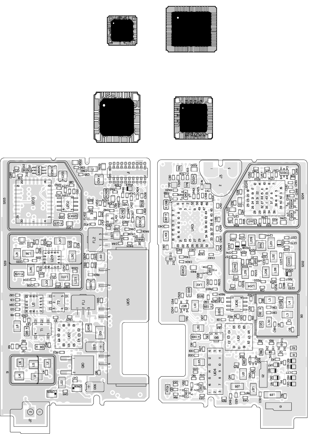
DIGITAL BOARD (A100)
Part No. 023-5005-100/-105
C 001 .1 µF +80/–20% Z5U 25V cer smd 510-3680-104
C 002 .1 µF +80/–20% Z5U 25V cer smd 510-3680-104
C 003 .1 µF +80/–20% Z5U 25V cer smd 510-3680-104
C 004 .1 µF +80/–20% Z5U 25V cer smd 510-3680-104
C 005 .1 µF +80/–20% Z5U 25V cer smd 510-3680-104
C 006 .1 µF +80/–20% Z5U 25V cer smd 510-3680-104
C 007 .1 µF +80/–20% Z5U 25V cer smd 510-3680-104
C 008 220 pF ±5% NPO 50V cer smd 510-3674-221
C 009 220 pF ±5% NPO 50V cer smd 510-3674-221
C 010 .1 µF +80/–20% Z5U 25V cer smd 510-3680-104
C 011 .1 µF +80/–20% Z5U 25V cer smd 510-3680-104
C 012 .1 µF +80/–20% Z5U 25V cer smd 510-3680-104
C 013 .1 µF +80/–20% Z5U 25V cer smd 510-3680-104
C 014 .1 µF +80/–20% Z5U 25V cer smd 510-3680-104
C 015 .1 µF +80/–20% Z5U 25V cer smd 510-3680-104
C 016 .1 µF +80/–20% Z5U 25V cer smd 510-3680-104
C 017 .1 µF +80/–20% Z5U 25V cer smd 510-3680-104
C 018 .1 µF +80/–20% Z5U 25V cer smd 510-3680-104
C 019 .1 µF +80/–20% Z5U 25V cer smd 510-3680-104
C 020 .1 µF +80/–20% Z5U 25V cer smd 510-3680-104
C 021 .1 µF +80/–20% Z5U 25V cer smd 510-3680-104
C 022 .1 µF +80/–20% Z5U 25V cer smd 510-3680-104
C 023 .1 µF +80/–20% Z5U 25V cer smd 510-3680-104
C 024 .1 µF +80/–20% Z5U 25V cer smd 510-3680-104
C 025 10 pF ±0.1 pF NPO 50V cer smd 510-3673-100
C 026 .1 µF +80/–20% Z5U 25V cer smd 510-3680-104
C 027 10 pF ±0.1 pF NPO 50V cer smd 510-3673-100
C 028 6.2 pF ±0.1 pF NPO 50V cer smd 510-3673-629
C 029 5.1 pF ±0.1pF NPO 50V cer smd 510-3673-519
C 030 470 pF ±5% NPO 50V cer smd 510-3674-471
C 031 470 pF ±5% NPO 50V cer smd 510-3674-471
C 032 .22 µF ±10% Z5U 25V cer smd 510-3686-224
C 033 220 pF ±5% NPO 50V cer smd 510-3674-221
C 034 220 pF ±5% NPO 50V cer smd 510-3674-221
C 035 .1 µF +80/–20% Z5U 25V cer smd 510-3680-104
C 036 .1 µF +80/–20% Z5U 25V cer smd 510-3680-104
C 037 220 pF ±5% NPO 50V cer smd 510-3674-221
C 038 220 pF ±5% NPO 50V cer smd 510-3674-221
C 039 220 pF ±5% NPO 50V cer smd 510-3674-221
C 040 220 pF ±5% NPO 50V cer smd 510-3674-221
C 041 470pF ±5% NPO 50V cer smd 510-3674-471
C 042 220 pF ±5% NPO 50V cer smd 510-3674-221
C 043 .1 µF +80/–20% Z5U 25V cer smd 510-3631-104
C 044 220 pF ±5% NPO 50V cer smd 510-3674-221
C 045 .1 µF +80/–20% Z5U 25V cer smd 510-3680-104
C 046 220 pF ±5% NPO 50V cer smd 510-3674-221
C 047 220 pF ±5% NPO 50V cer smd 510-3674-221
C 048 10pF ±0.1 pF NPO 50V cer smd 510-3673-100
C 049 10 pF ±0.1 pF NPO 50V cer smd 510-3673-100
C 050 33 pF ±10% X7R 25V cer smd 510-3675-330
C 051 33 pF ±10% X7R 25V cer smd 510-3675-330
C 052 470 pF ±5% NPO 50V cer smd 510-3674-471
C 053 470 pF ±5% NPO 50V cer smd 510-3674-471
C 054 470 pF ±5% NPO 50V cer smd 510-3674-471
C 055 470 pF ±5% NPO 50V cer smd 510-3674-471
C 056 220 pF ±5% NPO 50V cer smd 510-3674-221
C 057 .1 µF +80/–20% Z5U 25V cer smd 510-3680-104
C 058 470 pF ±5% NPO 50V cer smd 510-3674-471
C 059 470 pF ±5% NPO 50V cer smd 510-3674-471
C 060 .1 µF +80/–20% Z5U 25V cer smd 510-3680-104
C 061 220 pF ±5% NPO 50V cer smd 510-3674-221
C 062 220 pF ±5% NPO 50V cer smd 510-3674-221
C 063 .1 µF +80/–20% Z5U 25V cer smd 510-3680-104
C 064 .1 µF +80/–20% Z5U 25V cer smd 510-3680-104
C 065 220 pF ±5% NPO 50V cer smd 510-3674-221
C 066 .1 µF +80/–20% Z5U 25V cer smd 510-3680-104
C 067 220 pF ±5% NPO 50V cer smd 510-3674-221
C 068 .1 µF +80/–20% Z5U 25V cer smd
(-100 boards)
510-3680-104
220 pF ±5% NPO 50V cer smd
(-105 boards)
510-3674-221
C 069 .1 µF +80/–20% Z5U 25V cer smd
(-100 boards)
510-3680-104
220 pF ±5% NPO 50V cer smd
(-105 boards)
510-3674-221
C 070 220 pF ±5% NPO 50V cer smd 510-3674-221
C 071 220 pF ±5% NPO 50V cer smd 510-3674-221
C 072 220 pF ±5% NPO 50V cer smd 510-3674-221
Ref No. Description Part No.

PARTS LIST
6-2 September 2001
Part No. 001-5100-001
C 074 220 pF ±5% NPO 50V cer smd 510-3674-221
C 076 .1 µF +80/–20% Z5U 25V cer smd 510-3680-104
C 078 220 pF ±5% NPO 50V cer smd 510-3674-221
C 079 .1 µF +80/–20% Z5U 25V cer smd 510-3680-104
C 080 220 pF ±5% NPO 50V cer smd 510-3674-221
C 081 220 pF ±5% NPO 50V cer smd 510-3674-221
C 082 220 pF ±5% NPO 50V cer smd 510-3674-221
C 091 220 pF ±5% NPO 50V cer smd 510-3674-221
C 092 220 pF ±5% NPO 50V cer smd 510-3674-221
C 093 220 pF ±5% NPO 50V cer smd 510-3674-221
C 094 220 pF ±5% NPO 50V cer smd 510-3674-221
C 095 220 pF ±5% NPO 50V cer smd 510-3674-221
C 096 220 pF ±5% NPO 50V cer smd 510-3674-221
C 097 220 pF ±5% NPO 50V cer smd 510-3674-221
C 098 220 pF ±5% NPO 50V cer smd 510-3674-221
C 157 220 pF ±5% NPO 50V cer smd 510-3674-221
C 158 33 pF ±10% X7R 25V cer smd 510-3675-330
C 159 33 pF ±10% X7R 25V cer smd 510-3675-330
C 160 33 pF ±10% X7R 25V cer smd 510-3675-330
C 161 220 pF ±5% NPO 50V cer smd 510-3674-221
C 162 220 pF ±5% NPO 50V cer smd 510-3674-221
C 163 33 pF ±10% X7R 25V cer smd 510-3675-330
C 164 33 pF ±10% X7R 25V cer smd 510-3675-330
C 165 33 pF ±10% X7R 25V cer smd 510-3675-330
C 166 33 pF ±10% X7R 25V cer smd 510-3675-330
C 167 33 pF ±10% X7R 25V cer smd 510-3675-330
C 168 33 pF ±10% X7R 25V cer smd 510-3675-330
C 169 33 pF ±10% X7R 25V cer smd 510-3675-330
C 170 33 pF ±10% X7R 25V cer smd 510-3675-330
C 171 220 pF ±5% NPO 50V cer smd 510-3674-221
D 001 Diode, 1.5 pF SOT-23 523-1504-029
D 002 Zener diode, 5.6V SOT-23 523-2601-569
EP 101 Contact, power 013-1724-001
EP102 Z ground strip 017-1210-056
EP 103 Contact, battery pogo pin 515-9500-104
J 001 10-pin socket, x 2 515-7113-070
J 002 18-pin flex connector 515-7010-438
J 004 31-pin connector 515-7109-130
L 001 1.8 µH inductor, 350mA 542-9230-027
L 002-
L 036
Inductor, ferrite smd
(-100 boards)
542-9230-023
Ref No. Description Part No.
Inductor, ferrite smd
(-105 boards)
542-9230-021
MP 101 Shield, pogo 017-1210-053
PC 101 Flex circuit, power 035-1800-180
PC 100 PC board, digital trunking 035-5005-100
PC board, digital non-trunk 035-5005-105
PC101 Power flex circuit board, pogo pin 035-5005-101
Q 001 NPN general purpose SOT-23 576-0003-658
R 001 4.7k ohm ±5% 1/16W smd 569-0155-472
R 002 4.7k ohm ±5% 1/16W smd 569-0155-472
R 003 10k ohm ±5% 1/16W smd 569-0155-103
R 004 4.7k ohm ±5% 1/16W smd 569-0155-472
R 005 10k ohm ±5% 1/16W smd 569-0155-103
R 006 10k ohm ±5% 1/16W smd 569-0155-103
R 007 390k ohm ±5% 1/16W smd 569-0155-394
R 008 100k ohm ±5% 1/16W smd 569-0155-104
R 009 4.7k ohm ±5% 1/16W smd 569-0155-472
R 010 100k ohm ±5% 1/16W smd 569-0155-104
R 011 10k ohm ±5% 1/16W smd 569-0155-103
R 012 33k ohm ±5% 1/16W smd 569-0155-333
R 013 100k ohm ±5% 1/16W smd 569-0155-104
R 014 10k ohm ±5% 1/16W smd 569-0155-103
R 015 10k ohm ±5% 1/16W smd 569-0155-103
R 016 0 ohm jumper 569-0155-001
R 017 0 ohm jumper 569-0155-001
R 018 10k ohm ±5% 1/16W smd 569-0155-103
R 019 10k ohm ±5% 1/16W smd 569-0155-103
R 020 0 ohm jumper 569-0155-001
R 021 1.0M ohm ±5% 1/16W smd 569-0155-105
R 022 15k ohm ±5% 1/16W smd 569-0155-153
R 023 6.8k ohm ±5% 1/16W smd 569-0155-682
R 024 1k ohm ±5% 1/16W smd 569-0155-102
R 025 0 ohm jumper 569-0155-001
R 026 0 ohm jumper 569-0155-001
R 027 0 ohm jumper
(-100 board)
569-0155-001
47k ohm ±5% 1/16W smd
(-105 board)
569-0155-473
R 028 0 ohm jumper
(-100 board)
569-0155-001
Ref No. Description Part No.
DIGITAL BOARD (CONT’D)

PARTS LIST
6-3 September 2001
Part No. 001-5100-001
100k ohm ±5% 1/16W smd
(-105 board)
569-0155-104
R 029 47k ohm ±5% 1/16W smd 569-0155-473
R 030 1k ohm ±5% 1/16W smd
(-100 board)
569-0155-102
0 ohm jumper
(-105 board)
569-0155-001
R 031 10 ohm ±5% 1/16W smd 569-0155-100
R 032 10 ohm ±5% 1/16W smd 569-0155-100
R 033 0 ohm jumper
(-100 board)
569-0155-001
10k ohm ±5% 1/16W smd
(-105 board)
569-0155-103
R 034 22k ohm ±5% 1/16W smd 569-0155-223
R 035 22k ohm ±5% 1/16W smd 569-0155-223
R 036 22k ohm ±5% 1/16W smd 569-0155-223
R 037 0 ohm jumper 569-0155-001
R 038 0 ohm jumper 569-0155-001
R 039 10k ohm ±5% 1/16W smd 569-0155-103
R 040 10k ohm ±5% 1/16W smd 569-0155-103
R 041 0 ohm jumper 569-0155-001
R 042 0 ohm jumper 569-0155-001
R 043 0 ohm jumper 569-0155-001
R 044 0 ohm jumper 569-0155-001
R 045 22k ohm ±5% 1/16W smd 569-0155-223
R 046 22k ohm ±5% 1/16W smd 569-0155-223
R 047 22k ohm ±5% 1/16W smd 569-0155-223
R 048 22k ohm ±5% 1/16W smd 569-0155-223
R 049 22k ohm ±5% 1/16W smd 569-0155-223
R 050 22k ohm ±5% 1/16W smd 569-0155-223
R 051 22k ohm ±5% 1/16W smd 569-0155-223
R 052 22k ohm ±5% 1/16W smd 569-0155-223
R 053 22k ohm ±5% 1/16W smd 569-0155-223
R 054 22k ohm ±5% 1/16W smd 569-0155-223
R 055 22k ohm ±5% 1/16W smd 569-0155-223
R 056 22k ohm ±5% 1/16W smd 569-0155-223
R 057 22k ohm ±5% 1/16W smd 569-0155-223
R 058 22k ohm ±5% 1/16W smd 569-0155-223
R 059 22k ohm ±5% 1/16W smd 569-0155-223
R 060 22k ohm ±5% 1/16W smd 569-0155-223
R 061 22k ohm ±5% 1/16W smd 569-0155-223
R 062 22k ohm ±5% 1/16W smd 569-0155-223
R 063 22k ohm ±5% 1/16W smd 569-0155-223
R 064 0 ohm jumper 569-0155-001
R 065 1k ohm ±5% 1/16W smd 569-0155-102
Ref No. Description Part No.
R 087 0 ohm jumper 569-0155-001
R 090 10k ohm ±5% 1/16W smd 569-0155-103
R 091 1k ohm ±5% 1/16W smd 569-0155-102
R 092 1k ohm ±5% 1/16W smd 569-0155-102
R 093 1k ohm ±5% 1/16W smd 569-0155-102
R 094 1k ohm ±5% 1/16W smd 569-0155-102
R 095 1k ohm ±5% 1/16W smd 569-0155-102
R 096-
R 100
0 ohm jumper 569-0165-001
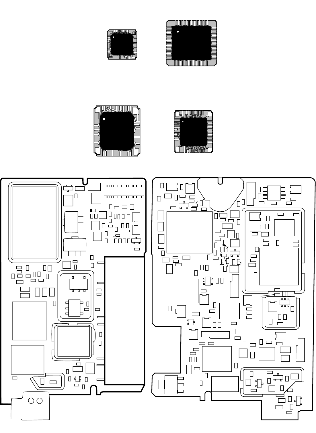
U 001 Programmable logic
(-100 board, revision 2)
544-1015-032
Microprocessor assembly
(-100 board, revision 3)
023-1870-043
Counter, preset 74HC161
(-105 board)
544-1010-161
U 002 Flash ROM 512k x 16 AT49
(-100 board)
544-1028-192
U 003 ADSIC, DSP supp BGA106
(all except following)
544-1010-015
ADSIC, DSP supp QFP package
(-100 board, rev 3)
544-9100-002
U 004 NAND, 2 Input TC7SHOOFU 544-1010-012
U 005 RAM 128k x 8 CY7C1009
(-100 board)
544-1011-028
SRAM, 64k x 8,IS61C512
(-105 board)
544-1011-026
U 006 RAM 128k x 8 CY7C1009
(-100 board)
544-1011-028
SRAM, 64k x 8,IS61C512
(-105 board)
544-1011-026
U 007 Rec/trans SCC2691 544-1012-691
U 008 EEPROM, 32k x 8 AT24C256W
(-100 board)
544-1020-256
PEROM, FLASH AT29C010A
(-105 board)
544-1010-010
U 009 NAND, 2-input TC7SH00FU
(-100 board)
544-1010-012
OR, 2-input TC7SH32FU
(-105 board)
544-1010-013
U 010 PEROM, FLASH AT29C010A 544-1010-010
U 011 OR, 2-input TC7SH32FU 544-1010-013
U 012 DSP TMS320C50PGEA 544-1010-018
U 021 D-flip flop TC7W74FU 544-1010-014
Y 001 Crystal,20.0000 MHz 521-3060-037
Y 002 Crystal,3.6864 MHz 521-3060-053
Ref No. Description Part No.
DIGITAL BOARD (CONT’D)

PARTS LIST
6-4 September 2001
Part No. 001-5100-001
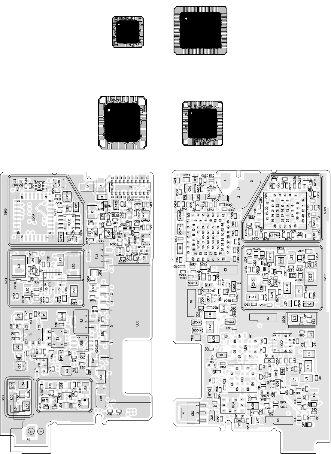
KEYPAD BOARD (A4xx)
Part No. 023-5005-4xx
A 430 DES interface board assembly 023-5005-430
C 001 .1 µF +80/–20% Z5U 25V cer smd 510-3680-104
C 002 .1 µF +80/–20% Z5U 25V cer smd 510-3680-104
C 003 .1 µF +80/–20% Z5U 25V cer smd 510-3680-104
C 004 .1 µF +80/–20% Z5U 25V cer smd 510-3680-104
C 005 330 pF ±10% X7R 25V cer smd 510-3675-331
C 006 220 pF ±5% NPO 25V cer smd 510-3674-221
C 007 .1 µF +80/–20% Z5U 25V cer smd 510-3680-104
C 008 .1 µF +80/–20% Z5U 25V cer smd 510-3680-104
C 009 .1 µF +80/–20% Z5U 25V cer smd 510-3680-104
C 010 22 pF ±5% NPO 25V cer smd 510-3674-220
C 011 2.7 pF ±10% NPO 25V cer smd 510-3674-279
C 012 .1 µF +80/–20% Z5U 25V cer smd 510-3680-104
C 013 22 pF ±5% NPO 25V cer smd 510-3674-220
C 014 4700 pF ±10% X7R 25V cer smd 510-3675-472
C 015 220 pF ±5% NPO 25V cer smd 510-3681-221
C 016 220 pF ±5% NPO 25V cer smd 510-3674-221
C 017 220 pF ±5% NPO 25V cer smd 510-3674-221
C 018 220 pF ±5% NPO 25V cer smd 510-3674-221
C 019 220 pF ±5% NPO 25V cer smd 510-3674-221
C 020 220 pF ±5% NPO 25V cer smd 510-3674-221
C 021 220 pF ±5% NPO 25V cer smd 510-3674-221
C 022 220 pF ±5% NPO 25V cer smd 510-3674-221
C 023 220 pF ±5% NPO 25V cer smd 510-3674-221
C 024 220 pF ±10% X7R 25V cer smd 510-3681-221
C 025 220 pF ±5% NPO 25V cer smd 510-3674-221
C 026 220 pF ±5% NPO 25V cer smd 510-3674-221
C 027 220 pF ±10% X7R 25V cer smd 510-3681-221
C 028 .01 µF ±10% X7R 25V cer smd 510-3675-103
C 029 220 pF ±5% NPO 25V cer smd 510-3674-221
C 030 220 pF ±5% NPO 25V cer smd 510-3674-221
C 031 220 pF ±10% X7R 25V cer smd 510-3681-221
C 032 220 pF ±10% X7R 25V cer smd 510-3681-221
C 033 100 pF ±5% NPO 25V cer smd 510-3674-101
C 034 10 pF ±0.1 pF NP0 50V cer smd 510-3673-100
C 035 220 pF ±5% NPO 25V cer smd 510-3674-221
C 036 220 pF ±5% NPO 25V cer smd 510-3674-221
C 037 220 pF ±5% NPO 25V cer smd 510-3674-221
C 038 33 pF ±5% NPO 50V cer smd 510-3601-330
C 039 100 µF 16V smd tantalum 510-2616-101
C 040 1 µF +80/–20% Z5U 25V cer smd 510-3631-105
Ref No. Description Part No.
C 041 220 pF ±10% X7R 25V cer smd 510-3681-221
C 042 220 pF ±5% NPO 25V cer smd 510-3674-221
C 043 1 µF +80/–20% Z5U 25V cer smd 510-3631-105
C 044 220 pF ±10% X7R 25V cer smd 510-3681-221
C 045 220 pF ±5% NPO 25V cer smd 510-3674-221
C 046 220 pF ±5% NPO 25V cer smd 510-3674-221
C 047 220 pF ±5% NPO 25V cer smd 510-3674-221
C 048 220 pF ±5% NPO 25V cer smd 510-3674-221
C 049 10 pF ±0.1 pF NP0 50V cer smd 510-3673-100
C 050 220 pF ±5% NPO 25V cer smd 510-3674-221
C 051 220 pF ±5% NPO 25V cer smd 510-3674-221
C 052 .1 µF +80/–20% Z5U 25V cer smd 510-3680-104
C 053 .1 µF +80/–20% Z5U 25V cer smd 510-3680-104
C 054 10 pF ±0.1 pF NP0 50V cer smd 510-3673-100
C 055 100 pF ±5% NPO 25V cer smd 510-3674-101
C 056 100 µF 10V smd tantalum 510-2624-100
C 057 .47 µF ±10% Z5U 16V cer smd 510-3605-474
C 058 4.7 µF 10V smd tantalum 510-2624-479
C 059 .1 µF +80/–20% Z5U 25V cer smd 510-3680-104
C 060 .1 µF +80/–20% Z5U 25V cer smd 510-3680-104
C 061 .1 µF +80/–20% Z5U 25V cer smd 510-3680-104
C 062 .47 µF ±10% Z5U 16V cer smd 510-3605-474
C 063 .1 µF +80/–20% Z5U 25V cer smd 510-3680-104
C 064 .47 µF ±10% Z5U 16V cer smd 510-3605-474
C 065 .47 µF ±10% Z5U 16V cer smd 510-3605-474
C 066 .1 µF +80/–20% Z5U 25V cer smd 510-3680-104
C 067 220 pF ±5% NPO 25V cer smd 510-3674-221
C 068 4.7 µF 10V smd tantalum 510-2624-479
C 069 .1 µF +80/–20% Z5U 25V cer smd 510-3680-104
C 070 220 pF ±5% NPO 25V cer smd 510-3674-221
C 071 220 pF ±5% NPO 25V cer smd 510-3674-221
C 072 220 pF ±5% NPO 25V cer smd 510-3674-221
C 073 220 pF ±5% NPO 25V cer smd 510-3674-221
C 074 100 pF ±5% NPO 25V cer smd 510-3674-101
C 075 .1 µF +80/–20% Z5U 25V cer smd 510-3680-104
C 076 220 pF ±5% NPO 25V cer smd 510-3674-221
C 077 .1 µF +80/–20% Z5U 25V cer smd 510-3680-104
C 078 .1 µF +80/–20% Z5U 25V cer smd 510-3680-104
C 079 1 µF +80/–20% Z5U 25V cer smd 510-3631-105
C 080 100 pF ±5% NPO 25V cer smd 510-3674-101
C 081 1 µF +80/–20% Z5U 25V cer smd 510-3631-105
C 082 .001 µF ±10% X7R 25V cer smd 510-3675-102
C 083 1 µF +80/–20% Z5U 25V cer smd 510-3631-105
C 084 220 pF ±10% X7R 50V cer smd 510-3681-221
C 085 220 pF ±5% NPO 25V cer smd 510-3674-221
Ref No. Description Part No.
KEYPAD BOARD

PARTS LIST
6-5 September 2001
Part No. 001-5100-001
C 086 220 pF ±5% NPO 25V cer smd 510-3674-221
C 087 100 pF ±5% NPO 25V cer smd 510-3674-101
C 088 220 pF ±5% NPO 25V cer smd 510-3674-221
C 089 220 pF ±5% NPO 25V cer smd 510-3674-221
C 090 220 pF ±5% NPO 25V cer smd 510-3674-221
C 091 10 pF ±0.1 pF NP0 50V cer smd 510-3673-100
C 092 1 µF +80/–20% Z5U 25V cer smd 510-3631-105
C 093 100 pF ±5% NPO 25V cer smd 510-3674-101
C 094 100 pF ±5% NPO 25V cer smd 510-3674-101
C 095 220 pF ±5% NPO 25V cer smd 510-3674-221
C 096 220 pF ±5% NPO 25V cer smd 510-3674-221
C 097 220 pF ±5% NPO 25V cer smd 510-3674-221
C 098 220 pF ±5% NPO 25V cer smd 510-3674-221
C 099 220 pF ±5% NPO 25V cer smd 510-3674-221
C 100 220 pF ±5% NPO 25V cer smd 510-3674-221
C 101 220 pF ±5% NPO 25V cer smd 510-3674-221
C 102 220 pF ±5% NPO 25V cer smd 510-3674-221
C 103 220 pF ±5% NPO 25V cer smd 510-3674-221
C 104 220 pF ±5% NPO 25V cer smd 510-3674-221
C 105 220 pF ±5% NPO 25V cer smd 510-3674-221
C 106 220 pF ±5% NPO 25V cer smd 510-3674-221
C 107 220 pF ±5% NPO 25V cer smd 510-3674-221
C 108 220 pF ±5% NPO 25V cer smd 510-3674-221
C 109 220 pF ±5% NPO 25V cer smd 510-3674-221
C 110 220 pF ±5% NPO 25V cer smd 510-3674-221
C 111 220 pF ±5% NPO 25V cer smd 510-3674-221
C 112 220 pF ±5% NPO 25V cer smd 510-3674-221
C 113 220 pF ±5% NPO 25V cer smd 510-3674-221
C 114 220 pF ±5% NPO 25V cer smd 510-3674-221
C 115 220 pF ±5% NPO 25V cer smd 510-3674-221
C 116 220 pF ±5% NPO 25V cer smd 510-3674-221
C 117 220 pF ±5% NPO 25V cer smd 510-3674-221
C 118 220 pF ±5% NPO 25V cer smd 510-3674-221
C 119 220 pF ±5% NPO 25V cer smd 510-3674-221
C 120 220 pF ±5% NPO 25V cer smd 510-3674-221
C 121 220 pF ±5% NPO 25V cer smd 510-3674-221
C 122 220 pF ±5% NPO 25V cer smd 510-3674-221
C 123 220 pF ±5% NPO 25V cer smd 510-3674-221
C 124 220 pF ±5% NPO 25V cer smd 510-3674-221
C 125 220 pF ±5% NPO 25V cer smd 510-3674-221
C 126 220 pF ±5% NPO 25V cer smd 510-3674-221
C 127 220 pF ±5% NPO 25V cer smd 510-3674-221
C 128 220 pF ±5% NPO 25V cer smd 510-3674-221
C 129 68 µF ±10% 16V tantalum 510-3674-221
C 130 220 pF ±5% NPO 25V cer smd 510-3674-221
Ref No. Description Part No.
C 131 220 pF ±10% X7R 25V cer smd 510-3681-221
C 132 47 pF ±5% NPO 25V cer smd 510-3674-470
C 133 47 pF ±5% NPO 25V cer smd 510-3674-470
C 134 47 pF ±5% NPO 25V cer smd 510-3674-470
C 135 1 µF +80/–20% Z5U 25V cer smd 510-3631-105
C 136 .1 µF +80/–20% Z5U 25V cer smd 510-3680-104
C 137 .01 µF ±10% X7R 25V cer smd 510-3675-103
C 138 1 µF +80/–20% Z5U 25V cer smd 510-3631-105
C 139 68 µF ±10% 16V tantalum 510-2625-680
C 140 68 µF ±10% 16V tantalum 510-2625-680
C 141 100 µF 16V smd tantalum 510-2616-101
C 142 4.7 µF 10V smd tantalum 510-2624-479
C 143 4.7 µF 10V smd tantalum 510-2624-479
C 144 68 µF ±10% 16V tantalum 510-3674-221
C 146 220 pF ±10% X7R 25V cer smd 510-3674-221
C 147 3900 pF ±10% X7R 25V cer smd 510-3675-392
C 148 220 pF ±10% X7R 25V cer smd 510-3681-221
C 149 220 pF ±10% X7R 25V cer smd 510-3681-221
C 150 220 pF ±10% X7R 25V cer smd 510-3681-221
C 151 220 pF ±10% X7R 25V cer smd 510-3681-221
C 152 220 pF ±10% X7R 25V cer smd 510-3681-221
C 153 220 pF ±10% X7R 25V cer smd 510-3681-221
C 154 220 pF ±10% X7R 25V cer smd 510-3681-221
C 155 220 pF ±10% X7R 25V cer smd 510-3681-221
C 156 220 pF ±10% X7R 25V cer smd 510-3681-221
C 157 220 pF ±10% X7R 25V cer smd 510-3681-221
C 158 220 pF ±10% X7R 25V cer smd 510-3681-221
C 159 220 pF ±10% X7R 25V cer smd 510-3681-221
C 160 220 pF ±10% X7R 25V cer smd 510-3681-221
C 161 220 pF ±10% X7R 25V cer smd 510-3681-221
C 162 220 pF ±10% X7R 25V cer smd 510-3681-221
C 163 220 pF ±10% X7R 25V cer smd 510-3681-221
C 164 220 pF ±10% X7R 25V cer smd 510-3681-221
C 165 220 pF ±10% X7R 25V cer smd 510-3681-221
C 166 220 pF ±10% X7R 25V cer smd 510-3681-221
C 167 220 pF ±10% X7R 25V cer smd 510-3681-221
C 168 220 pF ±10% X7R 25V cer smd 510-3681-221
C 169 220 pF ±10% X7R 25V cer smd 510-3681-221
CR 400 Front display backlight 585-5000-001
D 001 5.6V zener SOT-23 523-2601-569
D 002 Diode MMBD301LT1 523-1504-040
D 004 5.6V zener SOT-23 523-2601-569
D 005 Schottky diode rectifier 523-0519-034
Ref No. Description Part No.
KEYPAD BOARD (CONT’D)

PARTS LIST
6-6 September 2001
Part No. 001-5100-001
D 007 5.6V zener SOT-23 523-2601-569
D 008 10V zener SOT-23 523-2601-100
D 009 10V zener SOT-23 523-2601-100
D 010 10V zener SOT-23 523-2601-100
D 011 Diode MMBD301LT1 523-1504-040
D 013 Diode MMBD301LT1 523-1504-040
D 014 Diode MMBD301LT1 523-1504-040
D 015 5.6V zener SOT-23 523-2601-569
D 017 LED, green SMD HSMG-C670 549-4101-019
D 019 LED, green SMD HSMG-C670 549-4101-019
D 020 LED, green SMD HSMG-C670 549-4101-019
D 021 LED, green SMD HSMG-C670 549-4101-019
D 022 LED, green SMD HSMG-C670 549-4101-019
D 023 10V zener SOT-23 523-2601-100
D 024 10V zener SOT-23 523-2601-100
D 025 5.1V zener SOT-23 523-2601-519
D 035 LED, green SMD HSMG-C670 549-4101-019
D 036 LED, green SMD HSMG-C670 549-4101-019
D 037 LED, green SMD HSMG-C670 549-4101-019
D 038 LED, green SMD HSMG-C670 549-4101-019
D 039 LED, green SMD HSMG-C670 549-4101-019
D 040 LED, green SMD HSMG-C670 549-4101-019
D 041 LED, green SMD HSMG-C670 549-4101-019
D 042 LED, green SMD HSMG-C670 549-4101-019
D 043 LED, green SMD HSMG-C670 549-4101-019
D 044 LED, green SMD HSMG-C670 549-4101-019
D 045 LED, reen SMD HSMG-C670 549-4101-019
DS 400 LCD glass, radio front 549-5000-002
EP 400 Grounding contact 537-5001-009
J 002 Connector, flex 18-pin 515-7010-438
J 004 Connector, microminiature 515-7113-073
J 005 24-pin socket, ZIF 515-9500-017
J 013 24-pin socket, ZIF 515-9500-017
L 002 1.8 µH 250 mA smd inductor 542-9230-027
L 003 33 µH 1.2A smd inductor 542-9230-025
L 004 Ferrite bead, 600 ohm smd 542-9230-035
L 005 Ferrite bead, 600 ohm smd 542-9230-035
L 006 Ferrite bead, 600 ohm smd 542-9230-035
L 007 Ferrite bead, 600 ohm smd 542-9230-035
L 008 Ferrite bead, 600 ohm smd 542-9230-035
L 009 Ferrite bead, 600 ohm smd 542-9230-035
L 010 Ferrite bead, 600 ohm smd 542-9230-035
Ref No. Description Part No.
L 011 Ferrite bead, 600 ohm smd 542-9230-035
L 012 Ferrite bead, 600 ohm smd 542-9230-035
L 013 Ferrite bead, 600 ohm smd 542-9230-035
L 014 Ferrite bead, 600 ohm smd 542-9230-035
L 015 Ferrite bead, 600 ohm smd 542-9230-035
L 016 Ferrite bead, 600 ohm smd 542-9230-035
L 017 Ferrite bead, 600 ohm smd 542-9230-035
L 018 Ferrite bead, 600 ohm smd 542-9230-035
L 019 Ferrite bead, 600 ohm smd 542-9230-035
L 020 Ferrite bead, 600 ohm smd 542-9230-035
L 021 Ferrite bead, 600 ohm smd 542-9230-035
L 022 Ferrite bead, 600 ohm smd 542-9230-035
L 023 Ferrite bead, 600 ohm smd 542-9230-035
L 024 Ferrite bead, 600 ohm smd 542-9230-035
L 025 Ferrite smd inductor 542-9230-023
L 026 Ferrite smd inductor 542-9230-023
L 027 Ferrite smd inductor 542-9230-023
L 028 Ferrite smd inductor 542-9230-023
L 029 Ferrite smd inductor 542-9230-023
L 030 Ferrite smd inductor 542-9230-023
L 031 Ferrite smd inductor 542-9230-023
L 032 Ferrite smd inductor 542-9230-023
L 033 Ferrite bead, 600 ohm smd 542-9230-035
L 034 Ferrite bead, 600 ohm smd 542-9230-035
L 035 Ferrite bead, 600 ohm smd 542-9230-035
L 036 Ferrite bead, 600 ohm smd 542-9230-035
L 037 Ferrite bead, 600 ohm smd 542-9230-035
L 038 Ferrite bead, 600 ohm smd 542-9230-035
L 039 Ferrite bead, 600 ohm smd 542-9230-035
L 040 Ferrite bead, 600 ohm smd 542-9230-035
L 041 Ferrite smd inductor 542-9230-023
L 042 Ferrite smd inductor 542-9230-023
L 043 Ferrite smd inductor 542-9230-023
L 044 Ferrite smd inductor 542-9230-023
L 045 Ferrite smd inductor 542-9230-023
L 046 Ferrite smd inductor 542-9230-023
L 047 Ferrite smd inductor 542-9230-023
L 048 Ferrite smd inductor 542-9230-023
L 049 Ferrite smd inductor 542-9230-023
L 050 Ferrite smd inductor 542-9230-023
L 053 Ferrite smd inductor 542-9230-023
L 054 Ferrite smd inductor 542-9230-023
L 055 Ferrite smd inductor 542-9230-023
L 056 Ferrite smd inductor 542-9230-023
L 057 Ferrite smd inductor 542-9230-023
Ref No. Description Part No.
KEYPAD BOARD (CONT’D)

PARTS LIST
6-7 September 2001
Part No. 001-5100-001
L 058 Ferrite smd inductor 542-9230-023
L 059 Ferrite smd inductor 542-9230-023
L 060 Ferrite smd inductor 542-9230-023
L 061 Ferrite smd inductor 542-9230-023
L 063 Ferrite smd inductor 542-9230-023
L 064 Ferrite smd inductor 542-9230-023
MP 400 Front LCD holder,stamped 014-2229-508
P 400 Elastomeric connector 515-9900-007
P 430 Header, 8-pin 515-9500-018
PC400 PC board, keypad 035-5005-400
PC430 PC board, DES interface 035-5000-030
Q 001 NPN general purpose SOT-23 576-0003-658
Q 002 NPN general purpose SOT-23 576-0003-658
Q 004 P-chan enh mode MOSFET 576-0003-707
Q 005 NPN general purpose SOT-23 576-0003-658
O 006 NPN general purpose SOT-23 576-0003-658
Q 007 NPN general purpose SOT-23 576-0003-658
Q 008 NPN general purpose SOT-23 576-0003-658
Q 009 NPN general purpose SOT-23 576-0003-658
0 010 NPN general purpose SOT-23 576-0003-658
Q 011 P-chan enh mode MOSFET 576-0003-707
Q 012 NPN general purpose SOT-23 576-0003-658
Q 013 NPN general purpose SOT-23 576-0003-658
Q 014 NPN general purpose SOT-23 576-0003-658
Q 015 P-chan enh mode MOSFET 576-0003-707
R 001 100k ohm ±5% 1/16W smd 569-0155-104
R 002 100k ohm ±5% 1/16W smd 569-0155-104
R 003 100k ohm ±5% 1/16W smd 569-0155-104
R 004 100k ohm ±5% 1/16W smd 569-0155-104
R 005 10k ohm ±5% 1/16W smd 569-0155-103
R 006 10k ohm ±5% 1/16W smd 569-0155-103
R 007 100k ohm ±5% 1/16W smd 569-0155-104
R 008 10k ohm ±5% 1/16W smd 569-0155-103
R 009 1k ohm ±5% 1/16W smd 569-0155-102
R 010 10k ohm ±5% 1/16W smd 569-0155-103
R 011 10k ohm ±5% 1/16W smd 569-0155-103
R 012 100k ohm ±5% 1/16W smd 569-0155-104
R 013 10k ohm ±5% 1/16W smd 569-0155-103
R 014 56k ohm ±5% 1/16W smd 569-0155-563
R 015 10k ohm ±5% 1/16W smd 569-0155-103
Ref No. Description Part No.
R 016 0 ohm jumper 569-0155-001
R 017 1.0M ohm ±5% 1/16W smd 569-0155-105
R 018 100k ohm ±5% 1/16W smd 569-0155-104
R 019 10k ohm ±5% 1/16W smd 569-0155-103
R 020 100k ohm ±5% 1/16W smd 569-0155-104
R 021 100k ohm ±5% 1/16W smd 569-0155-104
R 022 100k ohm ±5% 1/16W smd 569-0155-104
R 023 1k ohm ±5% 1/16W smd 569-0155-102
R 024 220 ohm ±5% 1/16W smd 569-0155-221
R 025 220 ohm ±5% 1/16W smd 569-0155-221
R 026 0 ohm jumper 569-0155-001
R 027 47k ohm ±5% 1/16W smd 569-0155-473
R 028 4.75k ohm ±1% 1/16W smd 569-0156-903
R 029 10k ohm ±5% 1/16W smd 569-0155-103
R 030 6.19k, ±1% 1/16W smd 569-0156-904
R 031 10k ohm ±5% 1/16W smd 569-0155-103
R 032 10k ohm ±5% 1/16W smd 569-0155-103
R 033 100k ohm ±5% 1/16W smd 569-0155-104
R 034 220 ohm ±5% 1/16W smd 569-0155-221
R 035 0 ohm jumper 569-0155-001
R 036 100k ohm ±5% 1/16W smd 569-0155-104
R 037 27k ohm ±5% 1/16W smd 569-0155-273
R 038 10k ohm ±5% 1/16W smd 569-0155-103
R 039 2k ohm ±5% 1/16W smd 569-0155-202
R 040 100k ohm ±5% 1/16W smd 569-0155-104
R 041 100k ohm ±5% 1/16W smd 569-0155-104
R 042 100k ohm ±5% 1/16W smd 569-0155-104
R 043 100k ohm ±5% 1/16W smd 569-0155-104
R 044 4.7k ohm ±5% 1/16W smd 569-0155-472
R 045 47k ohm ±5% 1/16W smd 569-0155-473
R 046 390 ohm ±5% 1/16W smd 569-0155-391
R 047 4.7k ohm ±5% 1/16W smd 569-0155-473
R 048 22k ohm ±5% 1/16W smd 569-0155-223
R 049 10k ohm ±5% 1/16W smd 569-0155-103
R 050 390 ohm ±5% 1/16W smd 569-0155-391
R 051 4.7k ohm ±5% 1/16W smd 569-0155-472
R 052 10k ohm ±5% 1/16W smd 569-0155-103
R 053 10k ohm ±5% 1/16W smd 569-0155-103
R 054 100k ohm ±5% 1/16W smd 569-0155-104
R 055 100k ohm ±5% 1/16W smd 569-0155-104
R 056 47k ohm ±5% 1/16W smd 569-0155-473
R 057 360k ohm ±5% 1/16W smd 569-0155-364
R 058 130k ohm ±5% 1/16W smd 569-0155-134
R 059 180k ohm ±5% 1/16W smd 569-0155-184
R 060 220 ohm ±5% 1/16W smd 569-0155-221
Ref No. Description Part No.
KEYPAD BOARD (CONT’D)

PARTS LIST
6-8 September 2001
Part No. 001-5100-001
R 061 150 ohm ±5% 1/8W smd 569-0115-151
R 062 1k ohm ±5% 1/16W smd 569-0155-102
R 063 100k ohm ±5% 1/16W smd 569-0156-104
R 064 27k ohm ±5% 1/16W smd 569-0155-273
R 065 22k ohm ±5% 1/16W smd 569-0155-223
R 066 10k ohm ±5% 1/16W smd 569-0155-103
R 067 100k ohm ±5% 1/16W smd 569-0155-104
R 068 2.2k ohm ±5% 1/16W smd 569-0155-222
R 069 220 ohm ±5% 1/16W smd 569-0155-221
R 070 220 ohm ±5% 1/16W smd 569-0155-221
R 071 220 ohm ±5% 1/16W smd 569-0155-221
R 072 47k ohm ±5% 1/16W smd 569-0155-473
R 073 220 ohm ±5% 1/16W smd 569-0155-221
R 074 220 ohm ±5% 1/16W smd 569-0155-221
R 075 220 ohm ±5% 1/16W smd 569-0155-221
R 076 220 ohm ±5% 1/16W smd 569-0155-221
R 077 220 Ohm ±5% 1/16W smd 569-0155-221
R 078 0 ohm jumper 569-0155-001
R 079 100k ohm ±5% 1/16W smd 569-0155-104
R 080 100k ohm ±5% 1/16W smd 569-0155-104
R 081 200k ohm ±5% 1/16W smd 569-0155-204
R 082 100k ohm ±5% 1/16W smd 569-0155-104
R 083 100k ohm ±5% 1/16W smd 569-0155-104
R 084 100k ohm ±5% 1/16W smd 569-0155-104
R 085 100k ohm ±5% 1/16W smd 569-0155-104
R 086 1k ohm ±5% 1/16W smd 569-0155-102
R 087 150k ohm ±5% 1/16W smd 569-0155-154
R 088 2.2k ohm ±5% 1/16W smd 569-0155-222
R 089 220 ohm ±5% 1/16W smd 569-0155-221
R 090 220 ohm ±5% 1/16W smd 569-0155-221
R 091 10k ohm thermistor 569-3004-041
R 092 2k ohm ±5% 1/16W smd 569-0155-202
R 093 0 ohm jumper 569-0155-001
R 094 0 ohm jumper 569-0155-001
R 095 150 ohm ±5% 1/8W smd 569-0115-151
R 096 220 ohm ±5% 1/16W smd 569-0155-221
Ref No. Description Part No.
R 097 220 ohm ±5% 1/16W smd 569-0155-221
R 098 510k ohm ±5% 1/16W smd 569-0155-514
R 099 150k ohm ±5% 1/16W smd 569-0155-154
R 100 27k ohm ±5% 1/16W smd 569-0155-273
R 101 100k ohm ±5% 1/16W smd 569-0155-104
R 102 100k ohm ±5% 1/16W smd 569-0155-104
R 103 0 ohm jumper 569-0155-001
R 104 0 ohm jumper 569-0155-001
R 108 1k ohm ±5% 1/16W smd 569-0155-102
R 109 220k ohm ±5% 1/16W smd 569-0155-224
R 110 0 ohm jumper 569-0155-001
R 111 100k ohm ±5% 1/16W smd 569-0155-104
R 112 150 ohm ±5% 1/16W smd 569-0115-151
R 113 150 ohm ±5% 1/16W smd 569-0115-151
R 114 100k ohm ±5% 1/16W smd 569-0155-104
R 116 Zero ohm jumper 569-0165-001
R 117 Zero ohm jumper 569-0165-001
R 118 Zero ohm jumper 569-0165-001
R 119 Zero ohm jumper 569-0115-001
U 001 Microprcsr, MC68HC708 (unrev bd) 023-1870-045
Microprcsr, MC68HC908 (rev bd) 544-9100-003
U 002 Analog MUX TC4W53FU 544-1010-011
U 003 EEPROM, 1K 2.5V 24LC02B 544-1012-402
U 004 Voltage detector, micropower 544-1027-665
U 005 RS-232 driver LTC13381G 544-1015-706
U 006 Audio amp, 0.5W w/vol control 544-2006-026
U 007 Audio amp, 0.5W w/vol control 544-2006-026
U 008 Analog MUX TC4W53FU 544-1010-011
U 009 Op amp, SO-8 MC33182D 544-1010-030
U 010 Op amp, SO-8 MC33182D 544-1010-030
U 011 LCD driver MC14LC5003 544-1010-017
U 012 DC-DC converter 5V MAX744AE 544-1010-744
U 013 Regulator, 5V LT11211ST-5 544-1011-121
U 014 Shift register, 8-bit 4094 544-3016-094
W 101 Wire, black 30 gauge solid 592-0080-069
Y 001 Crystal,4.9152 MHz 521-3060-023
Ref No. Description Part No.
KEYPAD BOARD (CONT’D)
6-9 September 2001
Part No. 001-5100-001
PARTS LIST
EXPLODED VIEWS
MP005 MP004 S020 (5) PC020 EP020
MP001
MP002
EP010
PC010
MP003
PARTS LIST
6-10 September 2001
Part No. 001-5100-001
MP101
NP101
MP102
MP104 S101 EP102 EP101
MP040
S040
PC040
R101
EP040
?
PARTS LIST
6-11 Revised October 2000
Part No. 001-5005-002
MP105
MP106
HW102
MP107
MP108
HW101
A051
MP109
MP114
MP115 MP116
MK101
W101
W102
MP110
MP111
MP112 SP101
MP113
W104
W103
PARTS LIST
6-12 September 2001
Part No. 001-5100-001
CH030
CH030
MP035
A035
MP032 MP033 MP030
A200
PC050
MP035
A100
J050
A030
PARTS LIST
6-13 September 2001
Part No. 001-5100-001
A050 DS401 MP401 A400 A401
NP102
A402 MP402
September 2001
Part No. 001-5100-001
8-1
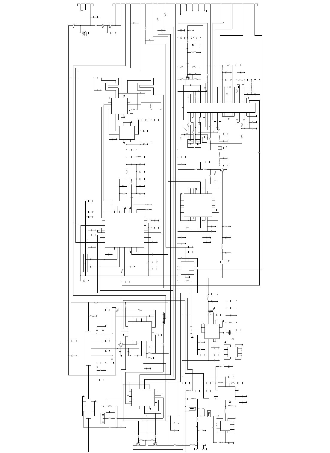
VHF RF BOARD SCHEMATIC
NOTE: Individual replacement parts are not available for the
RF board, so the entire board must be replaced if it is defective.
SECTION 8 SCHEMATIC DIAGRAMS AND COMPONENT LAYOUTS
September 2001
Part No. 001-5100-001
8-2
BOTTOM VIEW
TOP VIEW
TX 5V
THERM
INT CAP OUT
REF V
V CON CATH 1
TX 1
ANODE 2
RT BIAS
RX 1
TX 2
CATH 2
INT CAP IN
RF DET
GND
ANODE 1
RX 5V
BIAS EN
BIAS
B+2
ALC
62U72 X
XXYY X
U101
CE*
SC4
SC3
SC2
SC1
SW2
RX_D/A
TX_D/A
R/T
BIAS_EN
ANT_EN
REG5V
RESET
DATA
CLOCK
REF_D/A
GND
SW1
SWC
D/A
62U70 X
XXYY X
U102
FRAC N SYNTH
25U31 0
XXYY 0
VCP
ADAPT_SW
IADAPT
IOUT
MODOUT
CPBIAS 1
CPBIAS 2
TEST 2
VMULT 4
VMULT 3
VMULT 2
VMULT 1
FREFOUT
DC5
A/D BYPASS
XTAL 1
XTAL 2
A/D BYPASS
MODIN
CEX
CLK
DATA
DC5V
LOCK
AUX4
AUX3
AUX2
AUX1
SUPFCAP
SUPFBASE
SUPFOUT
SUPFIN
PREIN
DC5V
TEST 1
DC5V
PVREF
GND
U204
57W20
E28X
9307
REF1
SUB
SSL
OT
OTBY
OB
OGND
OVCC
VSSR
VDD
DGND
VDDH
ODC
CAPX
CAP
VPP
COL
EMIT
BASE
FLAG
IOUT
LGND
LVCC
DOUTX
DOUT
SBI
VCCP
LOX
LO
GND0
MOX
MO
T1C2
T1C
T1X
T1
T2C
T2X
T2
IFIN
GND1
IFIN2
VCCP2
BYP1
BYP2
IFI
DAFG
DAF
NLS
DAF2
GND
VCC
U401
VHF RF BOARD LAYOUT
September 2001
Part No. 001-5100-001
8-3
UHF RF BOARD SCHEMATIC
NOTE: Individual replacement parts are not available for the
RF board, so the entire board must be replaced if it is defective.
September 2001
Part No. 001-5100-001
8-4
BOTTOM VIEW
TOP VIEW
TX 5V
THERM
INT CAP OUT
REF V
V CON CATH 1
TX 1
ANODE 2
RT BIAS
RX 1
TX 2
CATH 2
INT CAP IN
RF DET
GND
ANODE 1
RX 5V
BIAS EN
BIAS
B+2
ALC
62U72 X
XXYY X
U101
CE*
SC4
SC3
SC2
SC1
SW2
RX_D/A
TX_D/A
R/T
BIAS_EN
ANT_EN
REG5V
RESET
DATA
CLOCK
REF_D/A
GND
SW1
SWC
D/A
62U70 X
XXYY X
U102
FRAC N SYNTH
25U31 0
XXYY 0
VCP
ADAPT_SW
IADAPT
IOUT
MODOUT
CPBIAS 1
CPBIAS 2
TEST 2
VMULT 4
VMULT 3
VMULT 2
VMULT 1
FREFOUT
DC5
A/D BYPASS
XTAL 1
XTAL 2
A/D BYPASS
MODIN
CEX
CLK
DATA
DC5V
LOCK
AUX4
AUX3
AUX2
AUX1
SUPFCAP
SUPFBASE
SUPFOUT
SUPFIN
PREIN
DC5V
TEST 1
DC5V
PVREF
GND
U204
57W20
E28X
9307
REF1
SUB
SSL
OT
OTBY
OB
OGND
OVCC
VSSR
VDD
DGND
VDDH
ODC
CAPX
CAP
VPP
COL
EMIT
BASE
FLAG
IOUT
LGND
LVCC
DOUTX
DOUT
SBI
VCCP
LOX
LO
GND0
MOX
MO
T1C2
T1C
T1X
T1
T2C
T2X
T2
IFIN
GND1
IFIN2
VCCP2
BYP1
BYP2
IFI
DAFG
DAF
NLS
DAF2
GND
VCC
U401
UHF RF BOARD LAYOUT
September 2001
Part No. 001-5100-001
8-5
CAPx
CAP
VPP
COL
EMIT
BASE
1 OUT
LGND
LVCC
46
47
48
49
50
51
1
2
3
DOUTx
DOUT
SB1
FLAG
ODC
VDDH
DGND
VDD
VSSR
OVCC
OGND
OB
OTBY
OT
SSL
SUB
REF 1
4
5
6
52
7
8
9
10
11
12
13
14
15
16
17
18
19
T2
T2x
T2c
T1
T1x
T1c
T1c2
45
44
43
42
41
40
39
MO
38
37
36
35
MOx
IF IN
GND1
IF IN 2
VCCP2
BYP1
BYP2
34
33
32
31
30
29
28
27
26
25
24
23
22
21
20 VCC
GND
DAF2
NLS
DAF
DAFS
IF1
VCCP
LOx
LO
GND0
ABACUS 11
U401
C421
.01uF
R414
2k
+C438
0.1uF
C419
0.1uF R412
33
Q1
C423
56pF
R418
1.5k
C424
56pF
R420
47k
C422
39pF
R419
47k
L402
180nH
C420
20pF
VR401
R416
20k
C426
0.22uF
R413
270
+C428
2.2uF
AUX2
AUX1
VCP
38
37
36
35
34
33
32
31
1ADAPT
ADAPTSW
GND6
1OUT
GND5
MODOUT
CPB1AS1
CPB1AS2
30
29
28
SUPFCAP
SUPFBASE
SUPFOUT
SUPFIN
PREIN
GND4
DC5V2
PVREF
DC5V3
TEST1
TEST2
GND3
XTAL2
XTAL1
GND2
A/D BYPASS
DC5V1
16
15
14
13
12
11
10
9
8
7
6VMULT4
VMULT3
VMULT2
VMULT1
FREFOUT
MODIN
CEX
CLK
DATA
GND1
GND7
GND6
DC5V4
LOCK
AUX4
AUX3
17 18 19 20 21 22 23 24 25 26 27
54321444342414039
TP302
R315
39k R309
51k
+C319
10uF
C320
33pF
+
C310
10uF
C309
.022uF
C372
0.1uF
C312
0.1uF
3
12
45
11 10 9
8
7
IN OUT
U201 6
13
1
2
C110
3.3pF
L104
RF INPUT
L201
17nH
L202
24nH
RF IN
1
8
RF
BYPASS GND
GND
B+
RF
BYPASS
GND RF OUT
U202
RF AMPLIFIER
4
5
23
L203
180nH
R202
10
+C201
10uF
C202
39pF
C203
100pF
76
C204
.022uF
L204
24nH
C222
6.2pF
3
12
45
11 10 9
8
7
IN OUT
U203 6
13
1
2
C223
5.1pF
MBP
GND
BDlv
13
14
12
11
RF
GND
RF MG2
GND
IFn
IFp
MVdd
3
4
5
6
211615
GND
LO IN
BBP
GND
10987
2
1
34
5
C218
.022uF
54
T202
123
C227
330pF
R204
100
+C210
10uF C211
.022uF
C212
39pF
C611
10pF
L605
750nH
C614
5.6pF
T201
Q503 REG 5V
1
2
5
4
3
RX D/A
TX D/A
R/T
REF D/A
GND
8
7
6
5
4
5V
ANT EN
BIAS EN
N/C
GND
RESET
32121 20 19
DAT
CLK
C.E.
SC4
SC3
U503
D/A IC
SW1
SW-C
SW2
SC1
SC2
9 10111213
18
17
16
15
14
INTCAP
C BIAS
V CON
INTCAP OUT
REF V
THERM
RFDET
GND1
ANODE1
CATH1
TX 11
ANODE2
BIAS RT
RX 1
TX 12
CATH2
B+2
U504
TX ALC IC
TX 5V
RX 5V
BIAS EN
BIAS
9 101112
8
7
6
5
4
318
17
16
15
14
13
C524
33pF
19
20
211
2
C517
33pF
C519
33pF
R514
10k
RT501
50k
R511
2k
+
C513
4.7uF
C523
33pF
C518
.022uF
C504
33pF
CR502 N/C
R501
10k
Q502
Q501
CR501
16
R508
6.8k
C503
33pF
R505
15k
R503
10k
C525
33pF
10 9
2
8
354
7
U501
COUPLER 7
65432
1
U502
RF PA
RF OUT
B+
RF IN
BIAS
BIAS
STABE 4 V/CON
STABE 3 V/CON
C510
.022uF
C509
33pF
C522
0.1uF
C505
33uF
+C18
1.0uF
E1
C512
.022uF
1
2
J2
L106
180nH
C114
33pF C101
20pF
L108
180nH
L105
C106
2.4pF L103
180nH
L102
15nH
C108
33pF L101
180nH
C105
33pF
C103
33pF
C213
.022uF
C209
.022uF
C226
39pF
C221
.022uF
C208
39pF +C216
10uF
C104
20pF C527
.022uF
CR102
CR104
C514
.022uF
C206
33pF
C207
3pF
R101
51k
C521
.022uF
+C520
10uF
C507
33pF
C506
33pF
R507
3.3k
C511
33pF
R508
1k
34 52
61
CR301
C301
0.1uF C302
0.1uF
C350
0.1uF
C303
100pF C313
0.1uF
C305
100pF
C370
4.3pF
R310
1k
C308
0.22uF
C328
100pF
C340
0.1uF
+C307
4.7uF C314
.022uF
N/C
N/C
C EXT
DET
DE
F OUT
V REG
V OPT
VDD
5
6
7
8
9
10
11
12
13
VDD
N/C
N/C
N/C
N/C
N/C
N/C
25
24
23
22
21
28
27
26
29
N/C
N/C
N/C
N/C
N/C
N/C
N/C
N/C
N/C
N/C
VSSD/VSSA
S1
SS
CE
SCK
SO
4321323130
14 191715 16 18 20
U304
18.8MHz
REF OSC
C353
.022uF
C354
33pF
R306
4.7k
C352
33pF
C351
.047uF
SENSE +5
SHDN
GND
B+ IN
FDBK
ERROR
5VTAP
U305
5V REG
3
4
8
7
21
56
C347
.022uF
R304
51k C345
0.1uF
C344
.022uF
+C348
10uF C349
.022uF
C322
0.1uF C317
0.1uF C318
0.1uF C329
0.1uF C330
0.1uF
RF IN
SW2
GND
GND
TRB
FL IP
GNDSW1
TX OUT
Vcc
RX OUT
GND
U303
VCO BUFFER
RXBB
N/C
PRE
TXBB
3
2
1
4
8765
9
10
11
12
13 14 15 16
R311
15k
C323
.022uF
GND
V CON
B+
SW1
SW2
OUT
2
1
9
V CON
GND
GND
U307
VCO
MODULE
5
6
34
87
C373
.022uF
C304
33pF C306
33pF
C373
.022uF
C315
1000pF
R307
1k
C324
.047uF
R314
51
R305
2k
C316
.022uF
C325
680pF
L302
10uH
C311
33pF
L301
15nH
C341
.022uF
C377
3pF
C339
12pF
C342
4.7pF
C408
.001uF
C425
2.2pF
R421
2.4k
C407
.01uF
C613
0.1uF
C406
.01uF
C403
.047uF
C404
0.1uF
+C405
3.3uF
C401
.033uF
R402
270k
C409
680pF
R403
27
R404
10k
L401
3.9uH
C410
75pF
R406
6.8k
C413
.01uF
VR402
C414
.0088uF
+
C417
3.3uF
+
C418
3.3uF
+
C430
10uF
R417
10
R407
47
C416
.01uF
C441
10000pF
C429
0.1uF
C415
0.1uF
C431
33pF
R411
68
1
3
2
1
3
2
C432
33pF
R410
68
L603
1100nH
FL402
450k
FL401
450k
R405
33
C605
3.6pF C606
7.5pF
R401
5.1
C433
0.1uF
+C450
10uF
L602
1500nH
L601
910nH
C604
4.3pF
C612
3pF
Q601
R605
3.3k
C602
0.1uF
R603
33k
FL2
73.35MHz
R602
2k
R601
100
C601
0.1uF
L600
910nH
FL1
73.35MHz
C609
3.3pF C610
7.5pF R604
12k
13
2
2
TP401
DOUT*
DOUT
SB1
DOC
RESET
1
2
TP400
4
8
6
18
16
12
5
3
7
DA CE
R327
0
CLOCK 10
C5
33pF
R326
0
R328
0
+C1
4.7uF
C2
.022uF
DATA 9
11
REF OSC EN
17
SW B+
SYN CE 14
15
MOD IN
13
LOCK DET
20
19
RAW B+
RAW B+
J1
(P1)
GND
J3
IS B+
RAW B+ IN
2
3
1
C14
33pF
+
C20
4.7uF
F001
2A
E3
E4
E2
VR1
C17
.022uF C15
.022uF
R509
1k
5V (RX)
0V (TX)
5V dc
0V (RX)
5V (TX)
6.0V (TX)
0V (RX)
5V (TX)
6.6V (TX)
7.6V (RX)
.37V (TX)
7.5V (RX)
0V (RX)
5V (TX)
7.4V (RX)
4.2V (TX) 5V dc 5V dc
5V dc
.43.43
2.5V dc2.5V dc
13V
3 - 11V dc
2.8V dc
4.6V 1.8V dc
5V
5V (TX)
0V (RX)
5V dc
.55 - .77V
7.5V dc
16.8MHz
4.7V dc
0V 4.7V
4.7V
4.7V
2.4V (RX)
4.8V (TX)
2.8V dc
2V dc
2.4 MHz
14.4MHz
.8V dc
3V dc
4.9V dc 4.9V dc
4.9V dc
2.1 MHz
STRIPLINE
STRIPLINE
C434
10nF C427
4.7nF
800 MHZ RF BOARD SCHEMATIC
NOTE: Individual replacement parts are not available for the
RF board, so the entire board must be replaced if it is defective.
September 2001
Part No. 001-5100-001
8-6
1
VR402
R503
C525
R505 C503
R506
7
CR501
CR501
C16
K
AA
E1
567
4
C523 C507
C510
U203
8
9
321
L102
L103
SH6
3
2U201
45
6
7
8
9
C110
J2 1
2
30
29
4
513
14
20
21
U304
C350
C322
L302
C370
R310
C372
R305
R307
C305
C304
C316
C323
C328
C303
SH7
U307
2
34
8
7
95
6
E2
C4
F001
VR1
KA
FL2
23
4
FL1
3
24
FL401
E4 E3
R416 VR401
FL402
C431
R411
3
3
1212
C424
L402
C420
C422
C423
C420
R418C440
C416 R420
C432
20 19
J1
(P1)
21
R327
C412
R417
R412
C434
R407
C427
C419
C430
C450
+
+
K
A
C413
C414
C409
R403
R406
R404
C342
R507
C614
C611
L605
T201
3
4
3
2
1
C227
C223
T202
54
32
1
C522
C508
C324
SH4
R314
C317
C318
C329
C353
SH5
654
321
U502
1
1
+
C512
Q501
BCE
RT501 C519
C505
C506
C504
C517
R511
R514
C513
+
AA
K
CR502
C216
+
A2 E2 C207
R509
Q502
123
R501
+
C520
U503
E2 E4
D5
D1
B1
A2 A4
B5
35
C511
C339
C403
C404
C405
+
R401 C441
C410
L401 +
C417
+
C418
C401
R402
TP400
19 17 15 13 11 9 7
6
4
2
52
20
22
24
26
28
30
32
2116 15 14 12 10 8
U401
5
3
1
23 57 62 70 75
25 56 61 65 69 74
55 60 64 68 73
54 59 63 67 72 51 50
49 48
27
29
31 53 58 66 71 47
34 36 38 40 42 44
33 35 37 39 41 43 45
46
C5
R419
R326
C1
+
C2
C20+
B
EC
Q1
TP401
R328
C433
R421
C408
C438 R414
C425
J3
2
3
C421
C426
L603
C605
C606
R413
C428
+
C413
L602
C604
L601
R601
R405
C429
C601
C406
C407
C613
C612
Q601
C
E
B
R605
C602
C610
R602
R603
C609
R604
L600
R508
G2
C218
C514
21
Q503
C521
C310
+
C319
+
C320
C206
C221
C226
10 7 6
14 1 2
U205
C209
C205
C213
C222
L204
L203
C204
C527
U504
A4 E4
G3
C518
+
C210
R204
U501
C108 L101 C105
AA
K
CR104
C106
L105 C104
A
AK
C103
L104
C102
CR102
L108
C107
LC114 R101
C101
K
A
A
VR2
SH3
G4
L201
L202
+
C201
C202
C201
C203
R202
SH2
C309
R306
C352
C351
C340
C307
+
3
1
4
6
CR301
C211
C212
C314
C315 R309
R315
TP302
C350
C301 C354
C302
U302
36 34 30 29 28
39 38 35 32 26 25
40 41 37 27 33 24 23
243 44 31
42
34613 15 22 19 20
16 5911 17 18
7810 14 12
21
C377
C311
C323 C313
C312
L301
R311 C341
C373
C321
15 14 12 11
7
6
4
3
1U303
C17
C15
G1
C306
C347
C345
U305
14
5
8
C344
R304
C349 C348
+
L106
210
57
C208
1
BOTTOM VIEW
TOP VIEW
TX 5V
THERM
INT CAP OUT
REF V
V CON CATH 1
TX 1
ANODE 2
RT BIAS
RX 1
TX 2
CATH 2
INT CAP IN
RF DET
GND
ANODE 1
RX 5V
BIAS EN
BIAS
B+2
ALC
62U72 X
XXYY X
U101
CE*
SC4
SC3
SC2
SC1
SW2
RX_D/A
TX_D/A
R/T
BIAS_EN
ANT_EN
REG5V
RESET
DATA
CLOCK
REF_D/A
GND
SW1
SWC
D/A
62U70 X
XXYY X
U102
FRAC N SYNTH
25U31 0
XXYY 0
VCP
ADAPT_SW
IADAPT
IOUT
MODOUT
CPBIAS 1
CPBIAS 2
TEST 2
VMULT 4
VMULT 3
VMULT 2
VMULT 1
FREFOUT
DC5
A/D BYPASS
XTAL 1
XTAL 2
A/D BYPASS
MODIN
CEX
CLK
DATA
DC5V
LOCK
AUX4
AUX3
AUX2
AUX1
SUPFCAP
SUPFBASE
SUPFOUT
SUPFIN
PREIN
DC5V
TEST 1
DC5V
PVREF
GND
U204
57W20
E28X
9307
REF1
SUB
SSL
OT
OTBY
OB
OGND
OVCC
VSSR
VDD
DGND
VDDH
ODC
CAPX
CAP
VPP
COL
EMIT
BASE
FLAG
IOUT
LGND
LVCC
DOUTX
DOUT
SBI
VCCP
LOX
LO
GND0
MOX
MO
T1C2
T1C
T1X
T1
T2C
T2X
T2
IFIN
GND1
IFIN2
VCCP2
BYP1
BYP2
IFI
DAFG
DAF
NLS
DAF2
GND
VCC
U401
800 MHZ RF BOARD LAYOUT
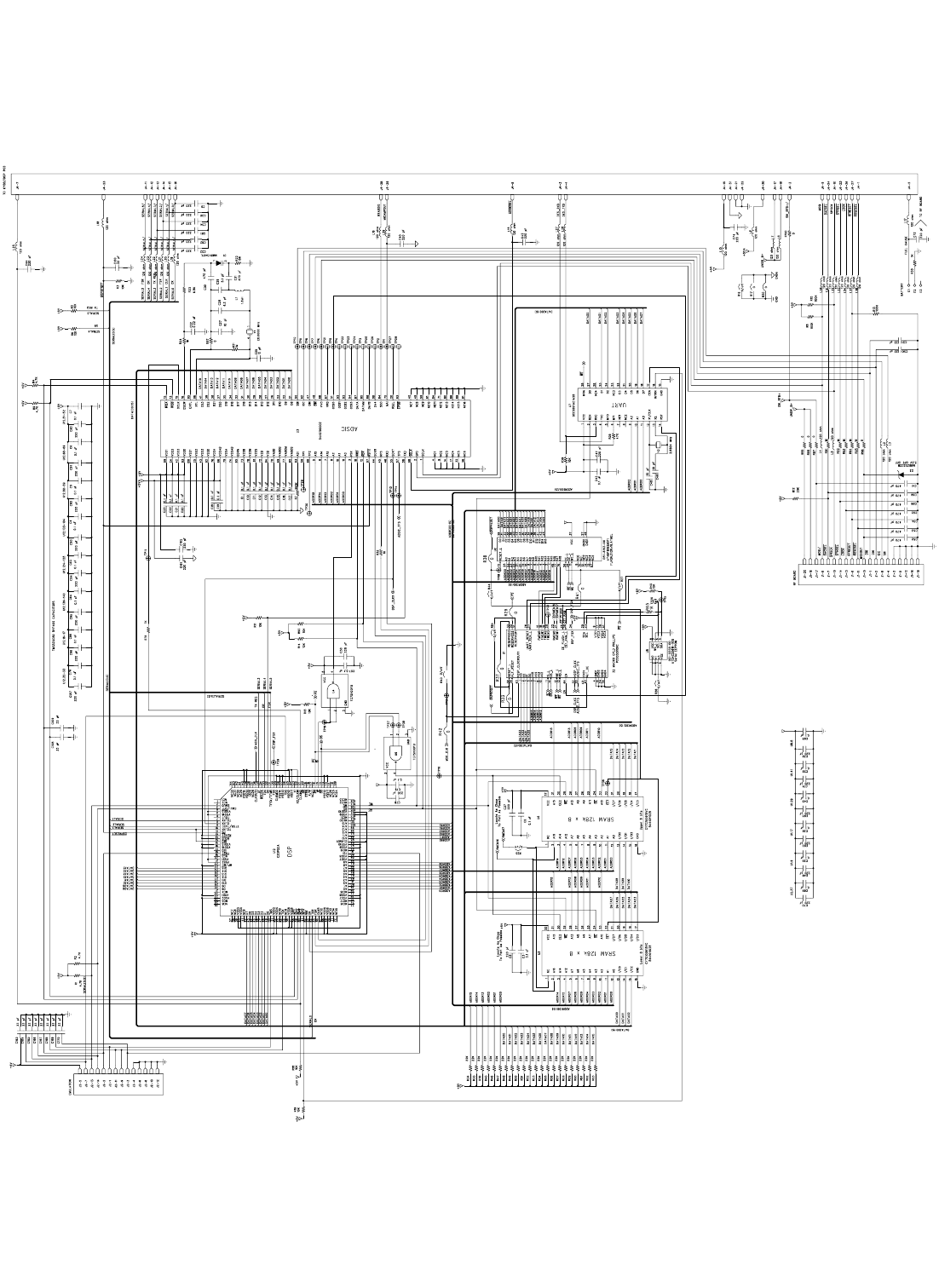
September 2001
Part No. 001-5100-001
8-7 LOGIC BOARD (REV. 3) SCHEMATIC
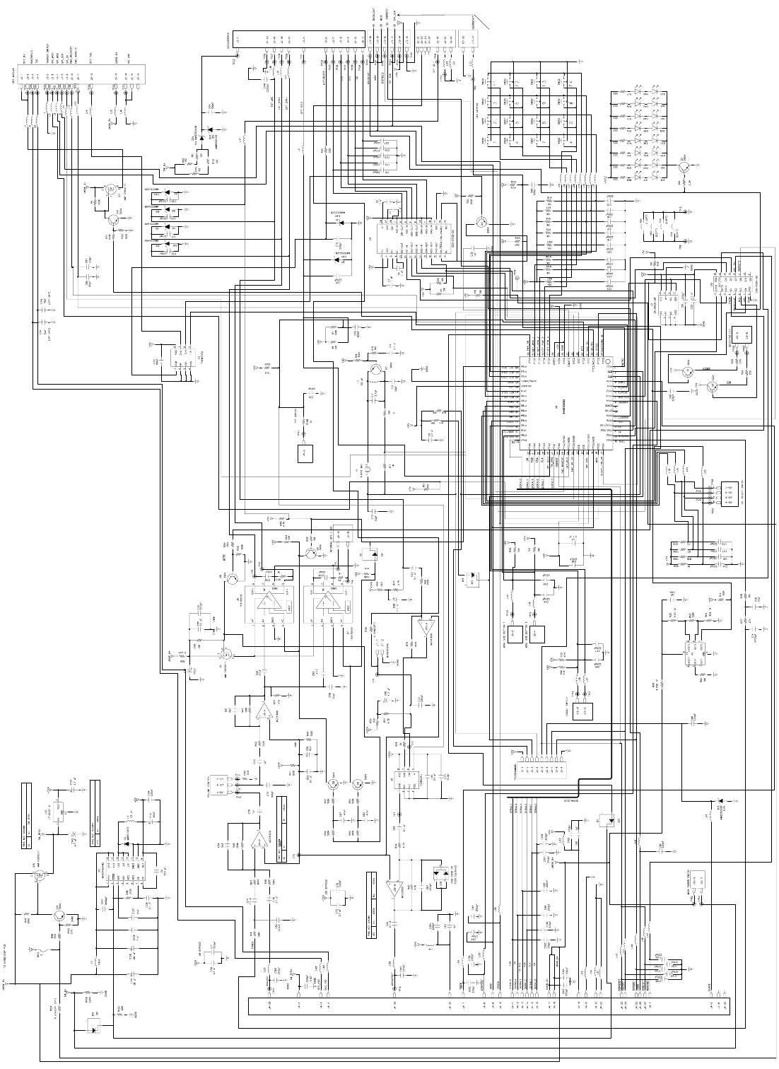
September 2001
Part No. 001-5100-001
8-8
To Front
Display
Schematic on
Page 8-16
REVISED KEYPAD BOARD SCHEMATIC