ELITEGROUP COMPUTER SYSTEMS ED2LN30PA1 DATA CARD User Manual Part 1
ELITEGROUP COMPUTER SYSTEMS CO., LTD DATA CARD Part 1
Contents
- 1. User Manual Part 1
- 2. User Manual Part 2
- 3. User Manual
User Manual Part 1


SPECIFICATIONS SUBJECT TO CHANGE WITHOUT NOTICE
Notice
While reasonable efforts have been made to assure the accuracy of this document, Telit
assumes no liability resulting from any inaccuracies or omissions in this document, or from
use of the information obtained herein. The information in this document has been carefully
checked and is believed to be entirely reliable. However, no responsibility is assumed for
inaccuracies or omissions. Telit reserves the right to make changes to any products described
herein and reserves the right to revise this document and to make changes from time to time
in content hereof with no obligation to notify any person of revisions or changes. Telit does
not assume any liability arising out of the application or use of any product, software, or
circuit described herein; neither does it convey license under its patent rights or the rights of
others.
It is possible that this publication may contain references to, or information about Telit
products (machines and programs), programming, or services that are not announced in your
country. Such references or information must not be construed to mean that Telit intends to
announce such Telit products, programming, or services in your country.
Copyrights
This instruction manual and the Telit products described in this instruction manual may be,
include or describe copyrighted Telit material, such as computer programs stored in
semiconductor memories or other media. Laws in the Italy and other countries preserve for
Telit and its licensors certain exclusive rights for copyrighted material, including the
exclusive right to copy, reproduce in any form, distribute and make derivative works of the
copyrighted material. Accordingly, any copyrighted material of Telit and its licensors
contained herein or in the Telit products described in this instruction manual may not be
copied, reproduced, distributed, merged or modified in any manner without the express
written permission of Telit. Furthermore, the purchase of Telit products shall not be deemed
to grant either directly or by implication, estoppel, or otherwise, any license under the
copyrights, patents or patent applications of Telit, as arises by operation of law in the sale of a
product.
Computer Software Copyrights
The Telit and 3rd Party supplied Software (SW) products described in this instruction manual
may include copyrighted Telit and other 3rd Party supplied computer programs stored in
semiconductor memories or other media. Laws in the Italy and other countries preserve for
Telit and other 3rd Party supplied SW certain exclusive rights for copyrighted computer
programs, including the exclusive right to copy or reproduce in any form the copyrighted
computer program. Accordingly, any copyrighted Telit or other 3rd Party supplied SW
computer programs contained in the Telit products described in this instruction manual may
not be copied (reverse engineered) or reproduced in any manner without the express written
permission of Telit or the 3rd Party SW supplier. Furthermore, the purchase of Telit products
shall not be deemed to grant either directly or by implication, estoppel, or otherwise, any
license under the copyrights, patents or patent applications of Telit or other 3rd Party supplied
SW, except for the normal non-exclusive, royalty free license to use that arises by operation
of law in the sale of a product.

Usage and Disclosure Restrictions
License Agreements
The software described in this document is the property of Telit and its licensors. It is
furnished by express license agreement only and may be used only in accordance with the
terms of such an agreement.
Copyrighted Materials
Software and documentation are copyrighted materials. Making unauthorized copies is
prohibited by law. No part of the software or documentation may be reproduced, transmitted,
transcribed, stored in a retrieval system, or translated into any language or computer language,
in any form or by any means, without prior written permission of Telit
High Risk Materials
Components, units, or third-party products used in the product described herein are NOT
fault-tolerant and are NOT designed, manufactured, or intended for use as on-line control
equipment in the following hazardous environments requiring fail-safe controls: the operation
of Nuclear Facilities, Aircraft Navigation or Aircraft Communication Systems, Air Traffic
Control, Life Support, or Weapons Systems (High Risk Activities"). Telit and its supplier(s)
specifically disclaim any expressed or implied warranty of fitness for such High Risk
Activities.
Trademarks
TELIT and the Stylized T Logo are registered in Trademark Office. All other product or
service names are the property of their respective owners.
Copyright © Telit Communications S.p.A. 2011.
Contents


Figure 1 M.2 HSPA+ Block Diagram................................................................................................................ 18
Figure 2 M.2 APAC LTE Module Block Diagram............................................................................................ 19
Figure 3 M.2 LTE Module Block Diagram........................................................................................................20
Figure 4 Detailed Interconnection of M.2 LTE Modem RF Engine ..................................................................21
Figure 5 PCI Express M.2 Module Interface ..................................................................................................... 22
Figure 6 GNSS Connections and Interface ........................................................................................................ 31
Figure 7 Typical LED Connection.....................................................................................................................36
Figure 8 Antenna Control – Connections Detail................................................................................................ 39
Figure 9 In-Device Coexistence Architecture.................................................................................................... 40
Figure 10 RF Antenna – Coaxial Connector Location....................................................................................... 46
Figure 11 M.2 Carrier Board.............................................................................................................................. 48
Figure 12 Windows 7 Software Architecture..................................................................................................... 52
Figure 13 Windows 8 Software Architecture..................................................................................................... 53
Figure 14 Linux Software Architecture ............................................................................................................. 55
Figure 15 Android Software Architecture..........................................................................................................59
Figure 16 Chrome Software Architecture ..........................................................................................................60
Figure 17 WWAN Card 3042 Mechanical Dimensions .................................................................................... 74
Figure 18 WWAN Card 3042 Slot Key Details.................................................................................................75
Figure 19 WWAN Card Type 3042 Top-Side Mounting Land Pattern.............................................................76
Figure 20 WWAN Card 3042 Mid-plane Land Pattern with Slot Key Removed..............................................77
Figure 21 Antenna Connector Location............................................................................................................. 78

Table 1 M.2 Module - General Feature..............................................................................................................14
Table 2. M.2 Module - RF Band Support ......................................................................................................... 15
Table 3. M.2 Module - Data Services................................................................................................................ 17
Table 4 M.2 Host Interface Signals.................................................................................................................... 22
Table 5 USB HS Interprocessor Communications Interface..............................................................................27
Table 6 USB SSIC – ICP Interface....................................................................................................................28
Table 7 (U)SIM Interface Signals...................................................................................................................... 29
Table 8 X-GOLD™ Baseband to GNSS Interface Signals................................................................................32
Table 9 GNSS Module Interface Signals ........................................................................................................... 32
Table 10 Power-on & Reset Signals .................................................................................................................. 33
Table 11 Radio Disable Signal........................................................................................................................... 34
Table 12 Host Radio Disable Interface (W_DISABLE#)..................................................................................35
Table 13 LED#1 Signal...................................................................................................................................... 36
Table 14 LED State Indicator ............................................................................................................................ 36
Table 15 Wake on WWAN Signal.....................................................................................................................37
Table 16 DPR#/ SAR Support Signal................................................................................................................ 38
Table 17 Tunable Antenna Control Signals .......................................................................................................39
Table 18 Coexistence – Hardware Synchronization Signals.............................................................................. 41
Table 19 Power & Ground Signals .................................................................................................................... 42
Table 20 M.2 Configuration Pins.......................................................................................................................43
Table 21 Audio Signals (Future development) ................................................................................................. 43
Table 22 No Connect Pins ................................................................................................................................. 45
Table 23 Antenna Requirements........................................................................................................................ 45
Table 24 Operating Environment....................................................................................................................... 61
Table 25 M.2 Module Power Delivery Requirements - Ultrabook.................................................................... 62
Table 26 VBAT Power Delivery Requirements – Direct Connections (Tablet)................................................62
Table 27 DC Specification for 3.3V Logic Signaling ........................................................................................63
Table 28 DC Specification for 1.8V Logic Signaling ........................................................................................63
Table 29 LTE Power Consumption.................................................................................................................... 64
Table 30 UMTS Power Consumption................................................................................................................ 64
Table 31 GSM Power Consumption .................................................................................................................. 65
Table 32 Conducted Transmit Power – 2G........................................................................................................67
Table 33 Conducted Transmit Power – 3G........................................................................................................67
Table 34 Conducted Transmit Power – LTE .....................................................................................................68
Table 35 Rx Sensitivity - GSM..........................................................................................................................68
Table 36 Rx Sensitivity - UMTS ....................................................................................................................... 69
Table 37 Rx Sensitivity - LTE...........................................................................................................................69
Table 38 Antenna Recommendation..................................................................................................................71
Table 39 Antenna Recommendation - Bandwidth of Main & Diversity Antenna............................................. 71
Table 40 GNSS Sensitivity................................................................................................................................ 72
Table 40 Antenna Connector Assignment ......................................................................................................... 78
This document is a technical specification for Telit’s next generation form factor M.2 module
family. The next generation form factor M.2 module family is a natural transition from the
PCI Express Mini Card and Half Mini Card to a smaller form factor size.
The M.2 Card Type 3042 offers single sided component mounting, 75 pins (8 dedicated for
key), in a compact size (30 mm x 42 mm). A range of 2G/3G/4G (LTE) M.2 modules
supporting multiple operating systems and unique features in the WWAN Card Type 3042
form factor are available.
The document will cover the features of the M.2 modules presently available. It will also
identify the M.2 module application interface along with hardware, software, reliability, and
mechanical specifications.
The intent of this document is to provide design guidelines and information for each M.2
module.
In addition to the M.2 module family features and performance metrics, this document
describes the interface signals, operating conditions, physical and mechanical requirements of
the M.2 cards.
This document is intended for editors who are about to write or edit documentation for Telit.
For general contact, technical support, to report documentation errors and to order manuals,
contact Telit Technical Support Center (TTSC) at:
TS-EMEA@telit.com
TS-NORTHAMERICA@telit.com
TS-LATINAMERICA@telit.com
TS-APAC@telit.com
Alternatively, use:
http://www.telit.com/en/products/technical-support-center/contact.php
For detailed information about where you can buy the Telit modules or for recommendations
on accessories and components visit:
http://www.telit.com
To register for product news and announcements or for product questions contact Telit
Technical Support Center (TTSC).
Our aim is to make this guide as helpful as possible. Keep us informed of your comments and
suggestions for improvements.
Telit appreciates feedback from the users of our information.
This document contains the following chapters (sample):
“Chapter 1: “Introduction” provides a scope for this document, target audience, contact and
support information, and text conventions.
“Chapter 2: “Chapter two” gives an overview of the features of the product.
“Chapter 3: “Chapter three” describes in details the characteristics of the product.
“Chapter 6: “Conformity Assessment Issues” provides some fundamental hints about the
conformity assessment that the final application might need.
“Chapter 7: “Safety Recommendation” provides some safety recommendations that must be
follow by the customer in the design of the application that makes use of the AA99-XXX.
Danger – This information MUST be followed or catastrophic equipment failure or bodily
injury may occur.
Caution or Warning – Alerts the user to important points about integrating the module, if
these points are not followed, the module and end user equipment may fail or malfunction.
Tip or Information – Provides advice and suggestions that may be useful when
integrating the module.
All dates are in ISO 8601 format, i.e. YYYY-MM-DD.
TBA

This section will provide an overview of the standard features of a M.2 Card, information on
the various SKUs of 2G/3G/4G (LTE) M.2 modules along with a respective functional block
diagram of each SKU.
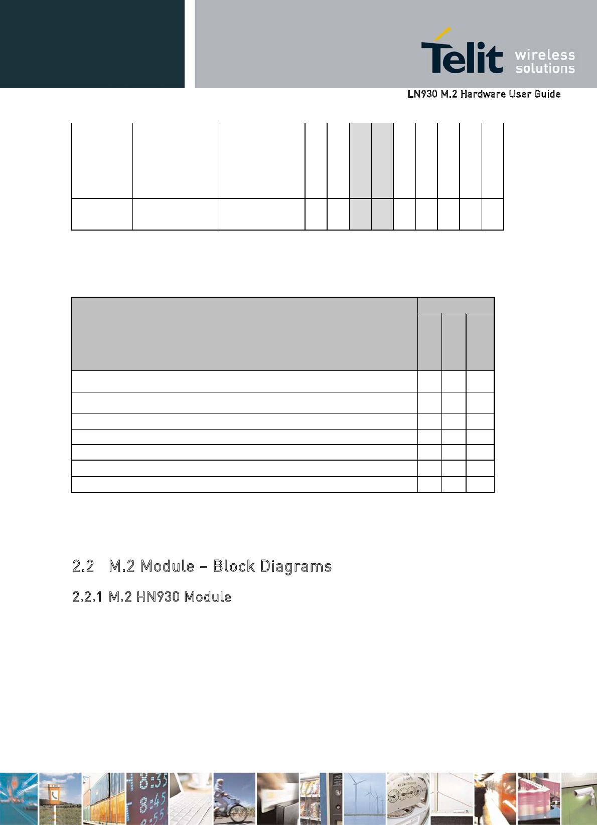
There are five different M.2 modules available in the M.2 Card Type 3042 form factor:
HN930 - HSPA+
LN930-AP - APAC LTE
LN930 - LTE
A comparison of the features, RF band Support, and data rates for the various M.2 modules is
shown in Table 1 through Table 3
Table 1 M.2 Module - General Feature
Feature Description Additional Information M.2 module
HN930
LN930-AP
LN930
Mechanical M.2 Card Type 3042
Slot B
30 mm x 42 mm
Pin count: 75
(67 usable, 8 slot) xxx
Operating
Voltage
3.3 V +/- 5% - xxx
Operating
Temperature
- – Normal
–
Extended
Extreme - This is the
surrounding air temperature of
the module inside the platform
when the card is fully operating
at worst case condition
xxx
Application
Interface
(75 pin card)
Interprocessor
Communications
USB 2.0 High-speed
xxx
USIM w/ Card Detect SIM_CLK, SIM_RESET,
SIM_IO, SIM_PWR,
SIM_DETECT
xxx
M.2 Control Full_Card_Power_On_Off xxx
Reset# xxx
W_DISABLE# xxx
LED #1 xxx
DPR (Body SAR) xxx
Wake on WWAN xxx
GNSS Disable xxx
Global Positioning
(GPS/ GLONASS)
I2C_SCL, I2C_SDA, I2_IRQ,
CLKOUT, TX_BLANKING xxx
Antenna Tuning (4) GPO (RF Transceiver) - x x
RF Coexistence (3) GPIO - x x
RF Antenna Main & Diversity/ GNSS Separate coax connectors xxx
Debug JTAG - xxx
ETM11 - - x x
MIPI PTI - - x X
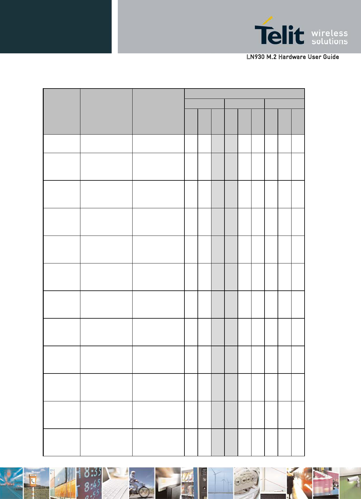
Table 2. M.2 Module - RF Band Support
RF Band UE Transmit UE Receive M.2 Module
HN930 LN930-AP LN930
GSM
UMTS
LTE
GSM
UMTS
LTE
GSM
UMTS
LTE
001 I
1920 MHz
-
1980 MHz
2
110 MHz
-
2170 MHz x x x x x
002 II
1850 MHz
-
1910 MHz
1930 MHz
-
1990 MHz x x x x x
003 III 1710 MHz -
1785 MHz
1805 MHz -
1880 MHz x x x x
004 IV 1710 MHz -
1755 MHz
2110 MHz -
2155 MHz x x x
005 V
824 MHz
-
849 MHz
869 MHz
-
894 MHz x x x x x
006 VI
830 MHz
-
840 MHz
875 MHz
-
885 MHz x
007 VII 2500 MHz -
2570 MHz
2620 MHz -
2690 MHz x
008 VIII
880 MHz
-
915 MHz
925 MHz
-
960 MHz x x x x x x x
009 IX 1749.9 MHz -
1784.9 MHz
1844.9 MHz -
1879.9 MHz x
010 X 1710 MHz -
1770 MHz
2110 MHz -
2170 MHz
011 XI
1427.9 MHz
-
1447.9 MHz
1475.9 MHz
-
1495.9 MHz x x
012 XII 699 MHz -
716 MHz
729 MHz -
746 MHz
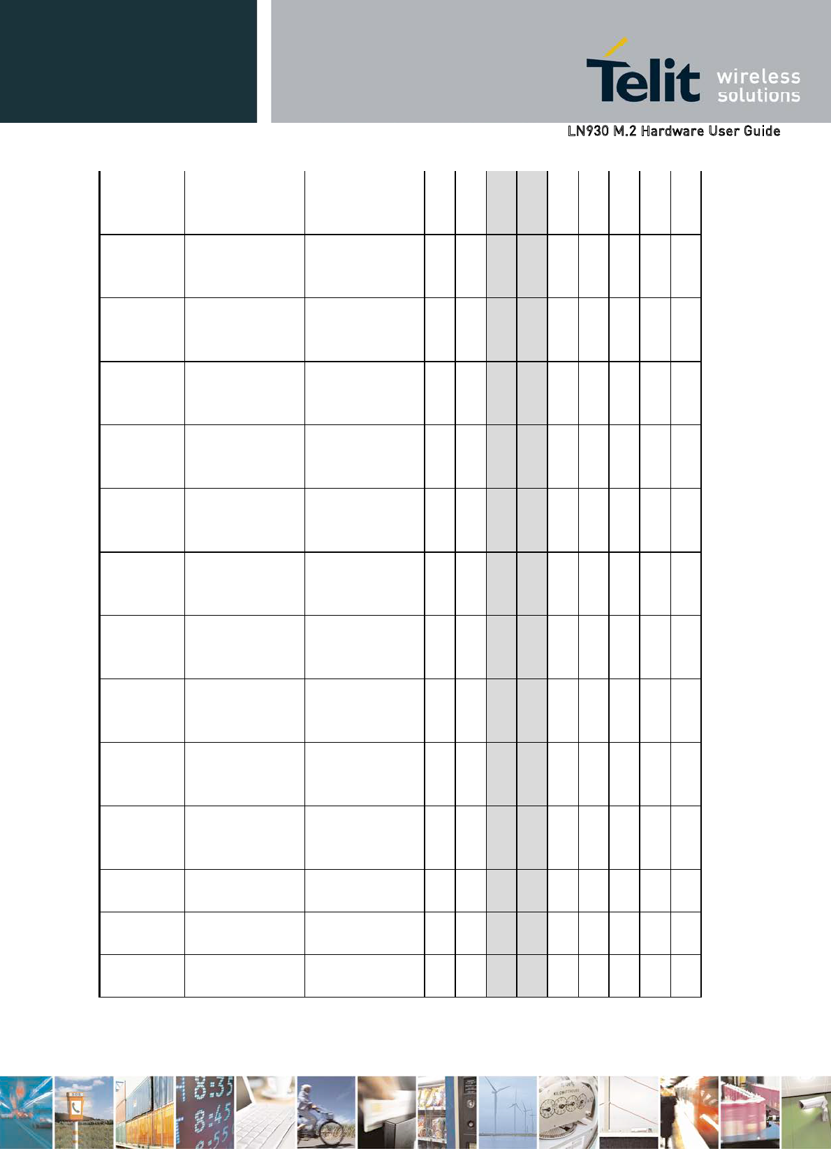
013 XI
II
777 MHz
-
787 MHz
746 MHz
-
756 MHz x
014 XIV
788 MHz
-
798 MHz
758 MHz
-
768 MHz
017 XVII 704 MHz -
716 MHz
7734 MHz -
746 MHz x
018 XVIII
815 MHz
-
830
MHz
860 MHz
-
875
MHz x x
019
XIX
830 MHz
-
845 MHz
875 MHz
-
890 MHz x x x
020 XX 832 MHz -
862 MHz
791 MHz -
821 MHz x
021 XXI
1447.9 MHz
-
1462.9 MHz
1495.9 MHz
-
1510.9 MHz x
022 XXII
3410 MHz
-
3490 MHz
3510 MHz
-
3590 MHz
023 XXIII 2000 MHz -
2020 MHz
2180 MHz -
2200 MHz
024 XXIV
1626.5 MHz
-
1660.5 MHz
1525 MHz
-
1559 MHz
025 XXV
1850 MHz
-
1915 MHz
1930 MHz
-
1995 MHz
026 XXVI 814 MHz -
849 MHz
859 MHz -
894 MHz x
027 XXVII 806 MHz -
824 MHz
851 MHz -
869 MHz
028 XXVIII
703 MHz -
748 MHz
758 MHz -
803 MHz
029 XXIX
1850 MHz
-
1910 MHz
or
1710 MHz -
1755 MHz
716 MHz
-
728 MHz
001 I
1920
MHz
-
1980 MHz
2110 MHz
-
2170 MHz
Table 3. M.2 Module - Data Services
Data Service M.2 module
HN930
LN930-AP
LN930
GPRS Class 33: DL 85.6 kbps, UL 85.6 kbps x - x
EDGE Class 33: DL 236.8 kbps, UL 236.8 kbps x - x
WCDMA: DL 384 kbps, UL 384 kbps
x
x
x
HSPA+: DL 21 Mbps, UL 5.7 Mbps x x x
HSPA+: DL 42 Mbps, UL 5.7 Mbps - x x
LTE FDD: DL: 100 Mbps, UL 50 Mbps - x x
LTE FDD: DL: 150 Mbps, UL 50 Mbps - x x
Module supports DL 150 Mbps in LN930. This is only for generic SW and VZW SW, but not
for AT&T SW.
The M.2 HSPA+ module is Intel’s Next Generation Form Factor design based on Intel’s
XMM™6260 modem platform. The M.2 HSPA+ card is a dual-mode (UMTS/GSM) 3GPP
release 7 HSPA+ modem.
The M.2 HSPA+ module includes support at the 75 pin application interface for
M.2 Control, USB 2.0 HS, GNSS, and USIM. Antenna Tuning is not supported.
A block diagram of the M.2 HSPA+ module is shown in Figure 1.
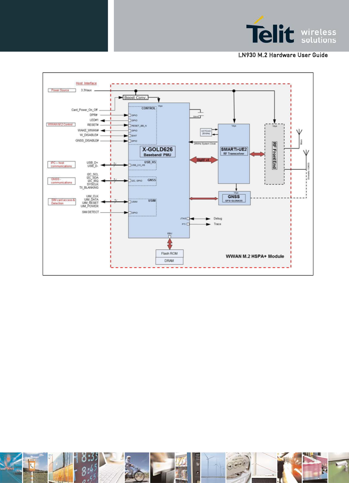
Figure 1 M.2 HSPA+ Block Diagram
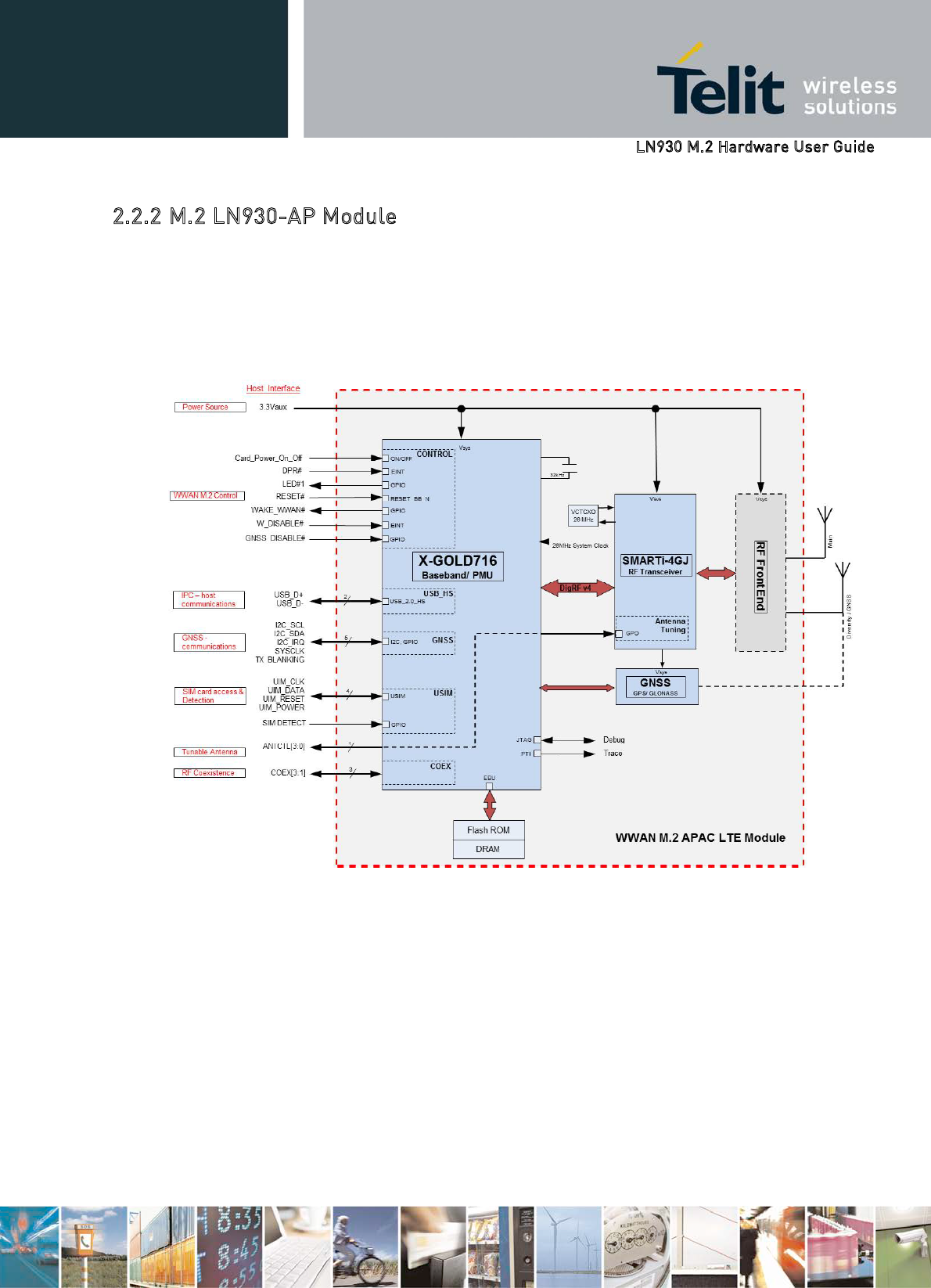
The M.2 APAC LTE module is another Intel design based on the XMM™7160 modem
platform. The module has a targeted area of operation in the Asia Pacific rim and offers 3G
and LTE datacard functionality, 2G Functionality is not supported.
The M.2 APC LTE module includes support at the 75 pin application interface for M.2
Control, USB 2.0 HS, GNSS, USIM and Antenna Tuning.
A block diagram of the M.2 APAC LTE module is shown in Figure 2.
Figure 2 M.2 APAC LTE Module Block Diagram
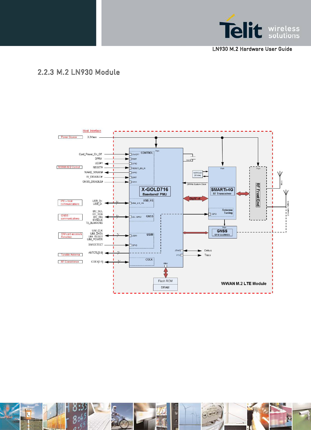
The M.2 LTE module is based on Intel’s XMM™7160 modem platform. The M.2 LTE
module is a triple-mode (2G, 3G, and 4G) 3GPP release 9 modem providing datacard
functionality.
The M.2 LTE module includes support at the 75 pin application interface for
M.2 Control, USB 2.0 HS, GNSS, USIM and Antenna Tuning.
A block diagram of the M.2 LTE module is shown in Figure 3.
Figure 3 M.2 LTE Module Block Diagram
A more detailed interconnect diagram of the RF Engine utilized on the M.2 LTE Module is
shown in Figure 4.
SMARTiTM 4G
PMB5740
RD_H1
RD_H1X
RD_H3
RD_H3X
RD_M1
RD_M1X
RD_L1
RD_L1X
RD_L2
RD_L2X
RD_L4
RD_L4X
Clock and
Control
DigRF
VBAT
SD2_1V8
AFC_DAC
REF OSC
XO_SUP
XO
VCTCXO
Measurement Unit
M1
M2
M3
Battery
RFE_NTC
RFE_PADCDC_MI
XOX
Diversity
Receiver
Combined
Receiver
RX_H2
RX_H2X
RX_H3
RX_H3X
RX_H4
RX_H4X
RX_M1
RX_M1X
RX_M2
RX_M2X
RX_L1
RX_L1X
RX_L2
RX_L2X
RX_L4
RX_L4X
RFFE
RFFE_VIO
RFFE_SDATA
RFFE_SCLK
Transmitter
TQ_X
TQ_H
TQ_L
TP_H
TP_L
PA Control
PADACS
PADACF
PADACF_P
FBR
FBR_RF1
FBR_RF2
XGOLDTM 716
B7
B1/B4
Diversity Switch &
Filter Module
Diversity
Antenna
RFE_RFFE_VIO
RFE_RFFE_SDATA
RFE_RFFE_SCLK
RFE_RFFE_VIO
RFE_RFFE_SCLK
RFE_RFFE_SDATA
Main Switch & Duplexer Module
B7 Duplexer
B7 Div Filter
B20 Div Filter
Coupler
Main
Antenna
RFE_RFFE_VIO
RFE_RFFE_SCLK
RFE_RFFE_SDATA
PA
DCDC
RFE_TQ_H
RFE_TP_H
RFE_TP_L
RFE_TQ_L
B2/B25
VBAT
VBAT
VBAT
B7 PA
RFE_PADCDC_MI
SCPA
RD_M2
RD_M2X
RD_L3
RD_L3X B20
RX_L3
RX_L3X
B2/B25
B3
B5/B26
B13/B17
B8
B20 Duplexer
B7
B20
B1
B4
B2/B25
B3
B5/B26
B8
B13/B17
B1
B4
B3
GSM_HB
GSM_ LB
B8
B5/B26
B20
B17
B13
VBAT
VBAT
Figure 4 Detailed Interconnection of M.2 LTE Modem RF Engine
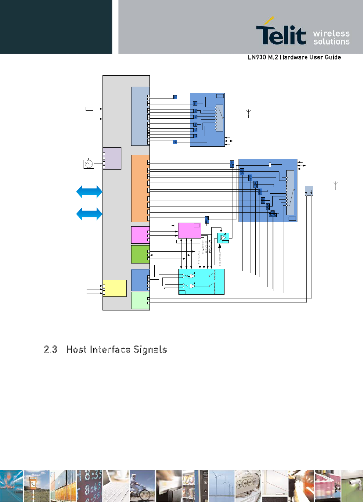
This section describes the signals available to the host processor at the 75 pin application
interface. Eight signals are eliminated by the notch on the host connector, leaving 67 usable
signals. A diagram of the M.2 module identifying the 75 pin interface is shown in Figure 5.
Note that the M.2 module has all components mounted on the top side. Odd pin numbers are on the top
side while even pins on the bottom side.
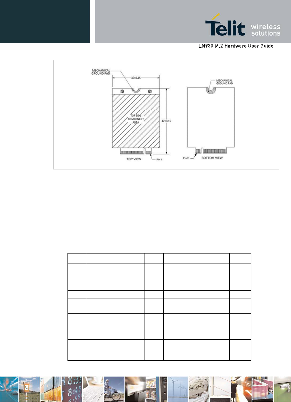
Figure 5 PCI Express M.2 Module Interface
A complete description of all interface signals available at the host interface is listed in Table
4. Some features, such as GNSS and Antenna Tuning, are not available on every M.2 module.
On those modules, the signals at the application interface are not connected on the M.2
module.
Table 4 M.2 Host Interface Signals
Pin
Signal Name
I/O
Description
Supply
1CONFIG_3 O Presence Indication:
WWAN M.2 Connects to GND
internally
-
2 3.3V
P
M.2 Supply Pin 3.3 V
3.3 V
3 GND
P
Ground
-
4 3.3V
P
M.2 LTE Supply Pin 3.3 V
3.3 V
5 GND
P
Ground
-
6 FULL_CARD_POWER_OFF#
I
Control signal to power On/Off
M.2.
1.8 V
7 USB D+
IO
USB 2.0 HS DPLUS Signal
8 W_DISABLE#
I
Active low signal to Disable
Radio Operation
3.3 V
9 USB D–
IO
USB 2.0 HS DMINUS Signal
10 LED#1
O
Open Drain, active low signal
used for add-in card to
provide status
3.3 V
11 GND
P
Ground
-
12 SLOT KEY
13 SLOT KEY
14 SLOT KEY
15 SLOT KEY
16 SLOT KEY
17 SLOT KEY
18 SLOT KEY
19 SLOT KEY
20 AUDIO0 IO PCM Clock (I2S_CLK) 1.8 V
21 CONFIG_0 O Configuration Status.
Presently not connected on
WWAN M.2 module.
-
22 AUDIO1 I PCM In (I2S_RX) 1.8 V
23 WAKE_WWAN#
O
Wake On WWAN
Use by M.2 to wake up host.
1.8 V
24 AUDIO2 O PCM Out (I2S_TX) 1.8 V
25 DPR
I
Dynamic Power Reduction -
Body SAR control signal
1.8 V
26 GNSS_DISABLE#
I
Disable GNSS function
1.8 V
27 GND
P
Ground
-
28 AUDIO3 IO PCM Sync (I2S_WA0) 1.8 V
29 SSIC_RxN
I
SSIC Receive N
(Not Supported)
-
30 UIM-RESET
O
SIM Reset (I)
1.8
V/3.0 V
31 SSIC_RxP
I
SSIC Receive P
(Not Supported)
-
32 UIM-CLK
O
SIM Clock (I)
1.8
V/3.0 V
33 GND
-
Ground
-
34 UIM-DATA
IO
SIM Data (I/O)
1.8
V/3.0 V
35 SSIC_TxN
O
SSIC Transmit N
(Not Supported)
-
36 UIM-PWR
O
SIM power
1.8
V/3.0 V
37 SSIC_TxP
O
SSIC Transmit P
(Not Supported)
-
38 N/C
-
Not connected internally on
M.2
-
39 GND
P
Ground
-
40 I2C_SCL
IO
I2C Clock – GNSS Support
1.8 V
41 N/C
-
Not connected internally on
M.2
-
42 I2C_SDA
IO
I2C Data – GNSS Support
1.8 V
43 N/C
-
Not connected internally on
M.2
44 I2C_IRQ
I
GNSS Interrupt Request –
GNSS Support
1.8 V
45 GND
P
Ground
-
46 SYSCLK
O
26 MHz reference Clock
output for external GNSS
module
1.8 V
47 N/C
-
Not connected internally on
M.2
-
48 TX_BLANKING
O
GNSS Blanking Signal used to
indicate 2G Tx burst and LTE
band 13 Tx burst.
1.8 V
49 N/C
-
Not connected internally on
M.2
-
50 N/C
-
Not connected internally on
M.2
-
51 GND
P
Ground
-
52 N/C
-
Not connected internally on
M.2
-
53 N/C
-
Not connected internally on
M.2
-
54 N/C
-
Not connected internally on
M.2
-
55 N/C
-
Not connected internally on
M.2
-
56 N/C
-
Not connected internally on
M.2
-
57 GND
P
Ground
-
58 N/C
-
Not connected internally on
M.2
-
59 ANTCTL0
O
RF Antenna Tuning Control
Signal 0
1.8 V
60 COEX3
O
Wireless Coexistence b
etween
WWAN and WiFi/BT
modules. IDC_LteDtxEnv
1.8 V
61 ANTCTL1
O
RF Antenna Tuning Control
Signal 1
1.8 V
62 COEX2
I
Wireless Coexistence between
WWAN and WiFi/BT
modules. IDC_CwsPriority
1.8 V
63 ANTCTL2
O
RF Antenna Tuning Control
Signal 2
1.8 V
64 COEX1
O Wireless Coexistence between
WWAN and WiFi/BT
modules. IDC_LteFrameSync
1.8 V
65 ANTCTL3
O
RF Antenna Tuning Control
Signal 3
1.8 V
66 SIM DETECT
I
SIM Card Detection (I) (low
active).
Pull-up resistor on WWAN
M.2 module
1.8 V
67 RESET#
I
Single control to reset WWAN
1.8 V
68 N/C
-
Not connected internally on
M.2
-
69 CONFIG_1 O Configuration Status
WWAN M.2 Connects to GND
internally
-
70 3.3V
P
WWAN Supply Pin 3.3 V
-
71 GND
P
Ground
-
72 3.3V
P
WWAN Supply Pin 3.3 V
-
73 GND
P
Ground
-
74 3.3V
P
WWAN Supply Pin 3.3 V
-
75 CONFIG_2 O Configuration Status
WWAN M.2 Connects to GND
internally
-
This section provides details on the various interfaces available M.2 modules.
There are two interfaces on the M.2 host interface that support interprocessor communications
(ICP); however, for the WWAN M.2 modules covered by the Product Description only the
USB 2.0 High-speed port will be supported.
The other ICP interface, USB Super-speed Inter-Chip (USB_SSIC), is not supported and the
signals should not be connected at the host.
The host processor, connected via an ICP interface, has access to the functions of the WWAN
card.
The USB 2.0 High-speed interface supports the following device classes: CDC-MBIM, CDC-
ACM, and CDC-NCM.
The USB Controller is compliant to the USB 2.0 Specification and with the Link Power
Management (LPM) Addendum. LPM introduces a new sleep state (L1) which significantly
reduces the transitional latencies between the defined power states; hence, improving the
responsiveness of the WWAN platform regarding connecting to the internet (Quick Connect).
USB2.0 LPM L1 Support
Support for OS assisted fast dormancy
Selective Suspend support
• Very low power when in Selective Suspend:
<4mw when connected to network (wake)
<1 mW no wake
It supports High-speed (HS, 480 MBit/s); Full-speed (FS, 12 MBit/s) transfers. Low- speed
mode is not supported. Because there is not a separate USB-controlled voltage bus, USB
functions implemented on the M.2 module are expected to report as self-powered devices
General Features
In device mode : High-speed (480 MBit/s) and Full-speed (12 MBit/s)
In host mode: High-speed (480 MBit/s), Full-speed (12 MBit/s). Low-speed mode (1.5
Mbit/s) is not supported.
Support for 16 bidirectional end points and channels including the end point 0.

Table 5 USB HS Interprocessor Communications Interface
Signal Name
Description
Pin
Direction
(WWAN)
Voltage
Level
USB_D+
USB Data Plus
7 I, O
Per USB 2.0
specification
USB_D–
USB Data
Minus
9 I, O
The USB Super-speed IC (USB SSIC) solution is not supported by the WWAN M.2 modules
presented in this Product Description. It is set aside for future development. These signals
should be left un-connected on the host.
Table 6 USB SSIC – ICP Interface
Signal Name
Description
Pin
Direction
(WWAN)
Operating
Voltage
Range
SSIC_RXN USB SSIC Receiver Signal N 29 O Per SSIC
specification
SSIC_RXP USB SSIC Receiver Signal P 31 O
SSIC_TXN USB SSIC Transmitter Signal N 35 I
SSIC_TXP USB SSIC Transmitter Signal P 37 I
The USIM interface is compatible with the ISO 7816-3 IC Card standard on the issues
required by the GSM 11.12 and GSM 11.18 standard.
Both 1.8 V and 3 V SIM Cards are supported.
A few comments on the SIM_DETECT signal
1. An external pull-up resistor is connected to SIM_DETECT on the WWAN M.2
module.
2. When a SIM is inserted, SIM_DETECT will be high.
3. When a SIM is removed or not present, SIM_DETECT will be low.
4. The host does not need to drive this signal. It can be tri-stated.
Table 7 (U)SIM Interface Signals
Signal Name
Description
Pin
Direction
(WWAN)
Voltage
Level
UIM_CLK
Clock SIM Card
32 O
1.8 V/3.0
V
UIM_DATA
Input/ Output SIM Card
34 I, O
1.8 V/3.0
V
UIM_RESET
Reset signal for SIM card
30 O
1.8 V/3.0
V
USIM_PWR
1.8 V/3 V Supply for SIM Card
36 O
1.8 V/3.0
V
SIM Detect
SIM Card Detection
66 I
1.8 V
The following design guidelines are recommended for the SIM card socket mounted on the
host system:
Length of the traces UIM_CLK, UIM_DATA, and UIM_RESET should not exceed
10 cm.
UIM_DATA is a sensitive open-drain bi-directional signal. It should not be mounted
beside the UIM_CLK signal for long distances. It is recommended to place the
UIM_RST trace between UIM_DATA and UIM_CLK to provide isolation. If the
traces are run a long distance, surround the UIM_DATA with ground to shield from
system noise and UIM_CLK.
The rise time for UIM_DATA should not exceed 1 µs per the 3GPP specification.
High input capacitance may increase rise time and lead to certification failure.
oKeep UIM traces with low capacitance between each other and to GND
oAn ESD component with high capacitance may increase rise time.
oThe pull-up current cannot be increased to speed up rise time, because the
pull-up current must not exceed 1 mA including any crosstalk.
oPull-up current is defined by the 4.7 k pull-up resistor (to USIM_PWR) on
the WWAN M.2 module, plus 200 µA from the baseband chip is
approximately 0.8 mA.
Place a decoupling capacitor close to the SIM card socket.
Some M.2 modules incorporate GPS and GLONASS receivers with aGPS to support
Global Positioning.
For M.2 modules that feature GNSS support, see Table 1, the M.2 module incorporates the
CG1960 Single-Chip GNSS Device, which is a complete receiver for simultaneous reception
and processing of both GPS and GLONASS signals. It includes LNA, mixer, bandpass filter,
VCO, ALC, fractional-N frequency synthesizer, digital tunable filters, PGA stage, and multi-
bit ADCs. A UART interface is used by the
X-GOLD™ Communications Processor on the M.2 module to control the GNSS device. The
solution offers best-in-class acquisition and tracking sensitivity, TFF and accuracy.
The GNSS device supports several different power management modes which gives the
lowest possible energy usage per fix. The pre-calculated location data will be sent over the
USB host interface. In addition, the M.2 will produce GPS data when the system is in sleep
mode via an I2C interface to allow for applications to be available in low power modes.
GNSS General Features
Autonomous GPS / GLONASS
Assisted GPS Using SUPL 1.0/2.0
• MS Assisted positioning ( SET / NET Initiated )
• MS Based positioning ( SET / NET Initiated )
SUPL 2.0 Feature Sets
Version Negotiation
Periodic Triggers
Emergency Positioning
Area Event Triggers (SET Init & NET Init)
Application ID
Enhanced Cell Id
Multiple Location IDs
Session Info Query
Location Transfer to 3rd Party
Notification Verification Based on Current Location
Location Request to another SET
A diagram of the GNSS connections on the M.2 module is shown in Figure 6. This diagram
identifies the signals between the X-GOLD™ baseband and GNSS devices along with the
USB and GNSS signals available to the host at the card interface.
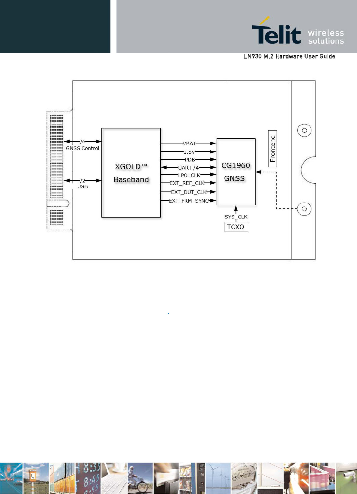
Figure 6 GNSS Connections and Interface
A description of the signals between the X-GOLD™ baseband and the CG1960
interface are defined in Table 8.
Table 8 X-GOLD™ Baseband to GNSS Interface Signals
Signal Description
VBAT Battery Supply
1.8V 1.8 V Supply provided from X-GOLD™ Baseband
UART The data and control I/F between the X-GOLD™ baseband and the GNSS
device is over a 4 wire UART interface which include CTS/RTS handshaking.
PDB X-GOLD™ baseband uses this signal to control Power-on/reset of the GNSS
device
LPO_CLK X-
GOLD™ baseband provides a permanently active 32 kHz clock to the GNSS
device
EXT_REF_CLK X-GOLD™ baseband provides a 26 MHz clock to the GNSS device for
frequency aiding.
EXT_DUT_CLK X-GOLD™ baseband provides this signal to notify the GNSS device of that
GSM Tx activity (PA Blanking)
EXT_FRM_SYNC X-GOLD™ baseband provides a strobe signal to the
GNSS device to allow fine
time assistance based on 3GPP cell timing.
The GNSS signals available to the host at the WWAN module interface to support
GNSS operation are shown in Table 9.
Table 9 GNSS Module Interface Signals
Signal Name Description Pin Direction
(WWAN)
Voltage
Level
I2C_SCL I2C Clock 40 I, O 1.8 V
I2C_SDA I2C Data 42 I, O 1.8 V
I2C_IRQ I2C IRQ - Interrupt signal 44 I 1.8 V
SYSCLK Synchronization Clock 46 I 1.8 V
TX_BLANKING TX Blanking – Active High when M.2 is
transmitting.
48 O 1.8 V
GNSS_DISABLE#
GNSS Disable
High: GNSS function is determine by AT
command.
Low: GNSS function is disabled.
GNSS_DISABLE# pin has a pull-up resistor
on the WWAN M.2 module
26 I 1.8 V
The system control interface is used to control the power-up and reset of the WWAN
module. There are additional control signals to disable the radio, drive an LED as a status
indicator, an output to wake the host processor, and an input for body SAR.
The host processor has two signals that can be used to power on and reset the modem.
Powering off the modem is accomplished through an AT command.
Table 10 Power-on & Reset Signals
Signal Name Description Pin Direction
(WWAN)
Voltage
Level
FULL_CARD_POWER_ON_OF
F
Modem power on:
For Tablet based designs
only; this signal is used for power on-off
control of
X-GOLD™ Baseband IC.WWAN M.2
module
Logic Low: M.2 Off
Logic High: WWAN M.2 Power On
This pin has an internal pull-down resistor.
Ultrabook designs:
Ultrabook host should deliver a 1.8V signal
to turn on the module. If 1.8V is not feasible,
recommend using a 47k series resistor
connected to 3.3V.
6 I 1.8 V
RESET# Reset the WWAN system. This signal is
used to reset the module.
This signal is part of the modem rigorous
power-off procedure. The host will first
assert this signal, followed by assertion of:
FULL_CARD_POWER_OFF# signal (for
Tablet)
Switch off 3.3V regulator (for Ultrabook)
Asserting RESET first is to trigger PMU
internal state machine to run shutdown
sequences e.g. for SIM and external
memory controller (EMIC), before
switching off power supplies.
Asynchronous, active low signal. When
active, the WWAN M.2 module will be
placed in a power–on reset condition.
RESET# pin has a pull-up resistor on the
WWAN M.2 module
67 I 1.8 V
An additional control signal is used to disable the radio on the module.
Signal W_DISABLE# is provided to allow users to disable, via a system-provided switch,
the add-in card’s radio operation in order to meet public safety regulations or when
otherwise desired. Implementation of this signal is required for systems and all add—in
cards that implement radio frequency capabilities.
The W_DISABLE1 signal is an active low signal that when driven low by the system shall
disable radio operation. The assertion and de-assertion of the W_DISABLE# signal is
asynchronous to any system clock. All transients resulting from mechanical switches need to
be de-bounced by the host system and no further signal conditioning will be required. When
the W_DISABLE# signal is asserted, all radios attached to the add-in card shall be disabled.
When the W_DISABLE# is not asserted or in a high impedance state, the radio may transmit
if not disabled by other means such as software.
The operation of the W_DISABLE# Signal is:
Enable, ON (3.3V): The radio transmitter is to be made capable of transmitting.
Disable, OFF (low): The radio transmitter(s) is to be made incapable of transmitting.
Standard TTL signaling levels shall be used making it compatible with 1.8 V and 3.3 V
signaling.
W_DISABLE# pin has a pull-up resistor on the M.2 module.
Table 11 Radio Disable Signal
Signal Name Detailed Description Pin Direction
(WWAN)
Voltage
Level
W_DISABLE#
Disable Radio.
This active low signal
allows the host to disable the M.2 radio
operation in order to meet public safety
regulations or when otherwise desired.
Logic Low: M.2 Off
Logic High: function is
determined by Software (AT
Command).
If this pin is left un-connected,
functionality is controlled by software.
Care should be taken not to activate this
pin unless there is a critical failure and
all other methods of regaining control
and/or communication with the M.2
module have failed.
8 I
Compatible
with
1.8 V/3.3
V
Standard TTL signaling levels shall be used.
Table 12 Host Radio Disable Interface (W_DISABLE#)
Requirement Detailed Description
Radio disable duration
On reception of a HW or SW disable signal, the WWAN module
will initiate within one second the mandatory cellular procedures
(which are dependent on current state) for disconnecting from
the cellular network. The time taken to complete the procedures
will be dependent on external factors including but not limited
to: 3G/4GPP specifications, network implementation, radio
conditions, etc. Once those procedures are complete, the WWAN
module will switch off the RF.
Radio enable duration On reception of a hardware or software enable signal the
WWAN module will initiate within one second the mandatory
cellular procedures for connecting to the cellular network.
Radio enable during selective suspend
If radio is disabled due to W_DISABLE# assertion and WWAN
module is in selective suspend, then W_DISABLE# de-assertion
shall be detected by WWAN module and the module shall
initiate exit from selective suspend.
An LED will be used to provide status indications to users via system provided
indicators.
LED#1 (pin 10) is an active low output signal intended to drive system-mounted LED
indicators. These signals shall be capable of sinking to ground a minimum of 9.0 mA at up to
a maximum VOL of 400 mV.
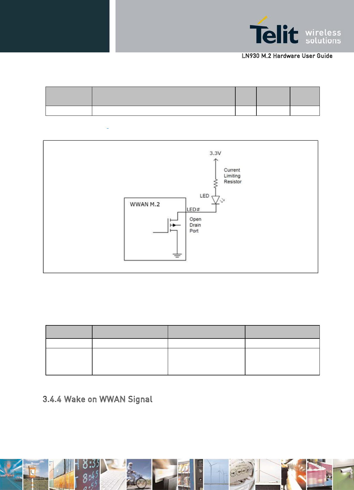
Table 13 LED#1 Signal
Signal Name Detailed Description Pin Direction
(WW
AN)
Voltage
Level
LED#1 LED Status Indicator 10 O (OD) 3.3 V
Figure 7 is an example of how an LED indicator is typically connected in a platform/system
using 3.3 V. The series resistor can be adjusted to obtain the desired brightness.
Figure 7 Typical LED Connection
The indication protocol for the LED is shown in Table 14.
Table 14 LED State Indicator
State Definition Characteristics WWAN
S
OFF The LED is emitting no - Not
ON The LED is emitting light
in a stable non-flashing
state
- Powered registered but
not transmitting or
receiving
An output signal is available to wake the host system, WAKE_WWAN#. This is an active
low, open-drain output.
This output requires a pull-up resistor on the host system.
Table 15 Wake on WWAN Signal
Signal Name Detailed Description Pin Direction
(WW
AN)
Voltage
Level
WAKE_WWAN# Used by M.2 module to wake the
host. Active Low, Open Drain output
23 O (OD) 3.0 V
With the arrival of Tablets and Ultrabook™ platforms where the antenna is in the base of the
unit, there is a significant issue passing Specific Absorption rate (SAR) requirements for
certification.
The WWAN M.2 module has the ability to configure RF TX power levels based on
proximity sensor input from the host.
A WWAN M.2 power control API is available to the host to dynamically reduce RF
transmit power levels of the WWAN module based on proximity sensor input from the
host.
The DPR# (Dynamic Power Reduction) signal is available on the host interface to assist in
meeting regulatory SAR (Specific Absorption Rate) requirements for RF exposure. The
signal is provided by a host system proximity sensor to the WWAN module to provide an
input trigger causing a reduction in the radio transmit output power.
In conjunction with the DPR signal, a full power control API is available to the host to
adjust the RF transmit power level of the WWAN module.
DPR pin has a pull-up resistor on the WWAN M.2 module.

Table 16 DPR#/ SAR Support Signal
Signal Name Detailed Description Pin Direction
(WW
AN)
Voltage
Level
DPR# Dynamic Power reduction. 25 I 1.8 V
In notebook platforms, since the WWAN antennas are usually located on the top of the lid,
there is a long RF mini-coax cable that can be up to 60 cm long between the antenna and
WWAN module, it is preferred to use switches/tunable components directly on the antenna
for antenna band switching/tuning to improve efficiency.
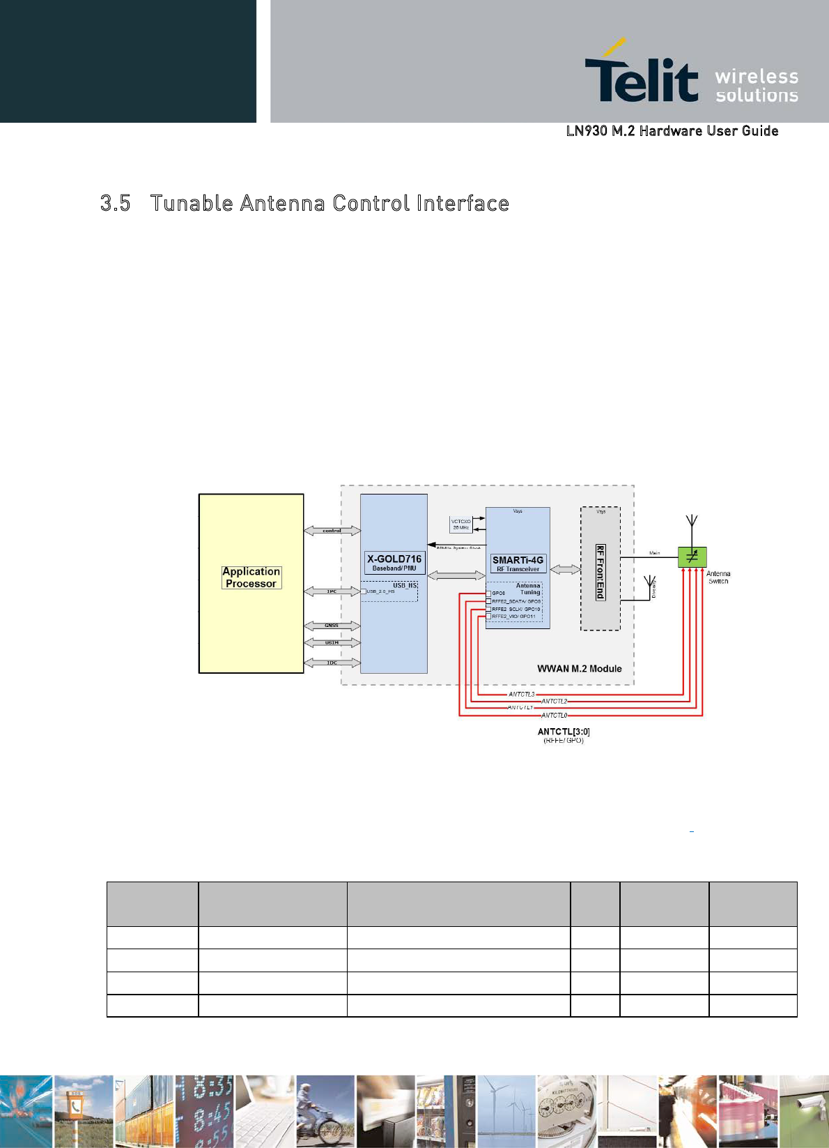
On select WWAN M.2 modules, four (4) GPOs are available on the host interface that can be
connected to an external antenna switch, to load the antenna with different impedances,
configuring the different frequency responses for the main antenna. A sample block diagram
depicting the antenna control signal connections to the antenna switch is shown in Figure 8.
Intel’s current antenna control solution offers an open loop control solution. The WWAN
M.2 modem expects the AP to provide the antenna profile detection and through a pre-
defined API, notify the WWAN M.2 modem with the correct antenna profile. The WWAN
M.2 modem then applies the proper antenna profile data accordingly.
Figure 8 Antenna Control – Connections Detail
The electrical specification for the antenna control GPIOs are shown in Table 17.
Table 17 Tunable Antenna Control Signals
Signal
Name
Description Smarti™ 4G Signal Pin Direction
(WWAN)
Voltage
Level
ANTCTL0 Antenna Control 0 GPO8 59 O 1.8V
ANTCTL1 Antenna Control 1 RFFE2_SDATA/ GPO9 61 O 1.8V
ANTCTL2 Antenna Control 2 RFFE2_SCLK/ GPO10 63 O 1.8V
ANTCTL3 Antenna Control 3 RFFE2_VIO/ GPO11 65 O
1
.
8V
As more and more radios are added to PC Ultrabook™ and tablet platforms, the sources RF
interference increases significantly as multiple radios will have overlapping transmissions
and receptions. This problem will increase further as overlapping bands continue to be rolled
out; WIFI, BT, WWAN will all use overlapping band from 2300 MHz to 2600 MHz.
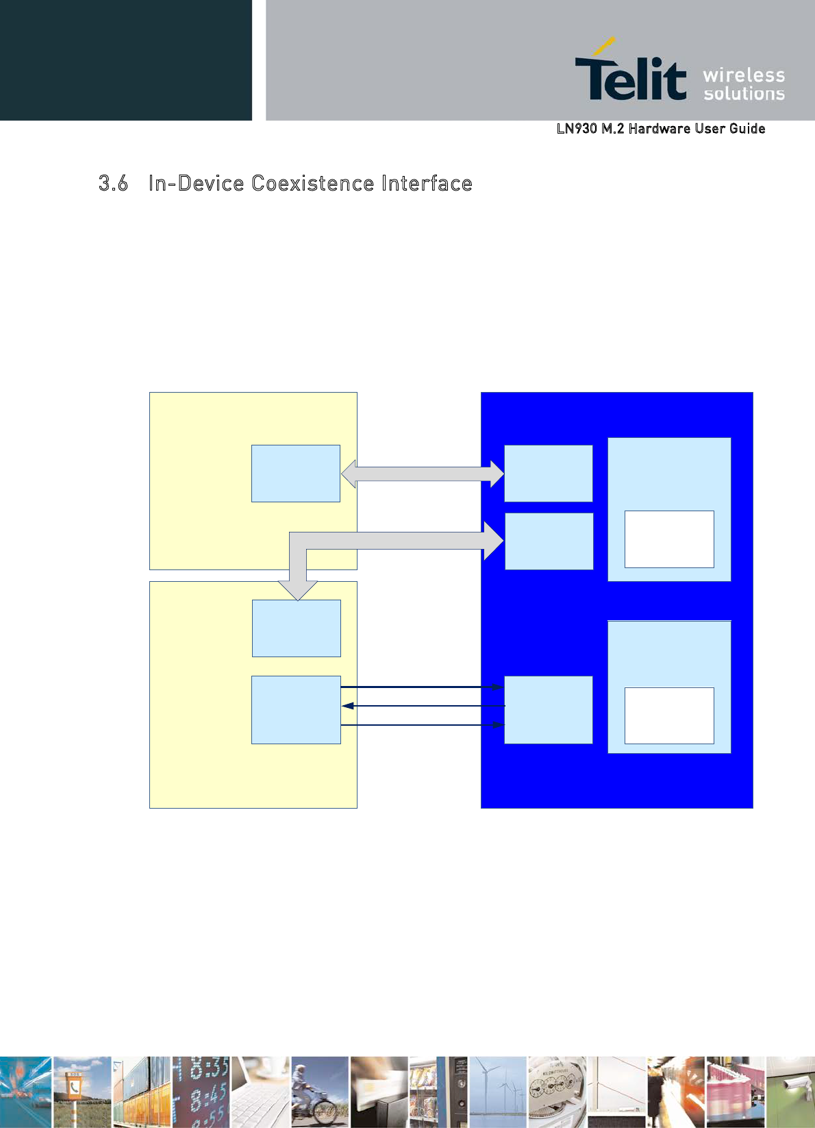
In-Device Coexistence is a feature which improves the user experience and maximizes
throughput and Quality of Service of connectivity systems (WLAN, BT and GNSS) when
these radios are simultaneously running with the WWAN M.2 LTE modem.
A diagram of the In-Device Coexistence architecture is shown in Figure 6.
Application
Processor
apps
coexistence
interface
Connectivity Chip
(WLAN/BT/GNSS)
NRT
Coexistence
interface
RT
Coexistence
interface
X-GOLD™ 716
apps
coexistence
interface
NRT
Coexistence
interface
RT
Coexistence
interface
CPU
NRT
coexistence
controller
LTE L1
RT
coexistence
controller
Message –based I/F)
IDC_CwsPriority
NRT Apps Coex I/F
Message –based I/F)
NRT Coex I/F
IDC_LteFrameSync
IDC_LteDtxEnv
Figure 9 In-Device Coexistence Architecture
Seamless Co-running
In-Device-Coexistence primarily aims at avoiding interference between radio systems to
allow seamless co-running where LTE and WLAN/BT/GNSS ensuring their maximum
throughput and performance. To do so, a Non Real Time (NRT) coexistence controller is
implemented on the ARM™ CPU. The NRT coexistence controller centralizes LTE, WLAN,
BT and GNSS information and performs interference avoidance mechanisms, selecting
interference-safe frequency configurations whenever possible. The NRT coexistence
controller is also in charge of enabling some Real Time (RT) coexistence mechanisms when
NRT mechanisms are not sufficient to guarantee seamless co-running of LTE and
connectivity systems (WLAN, BT, and GNSS).
Inter-system Synchronization
For the cases where co-running of LTE and connectivity systems cannot be achieved, a Real
Time (RT) coexistence controller is implemented in the LTE Layer-1 subsystem. The RT
coexistence controller is in control of the RT coexistence interface, which is exposed to the
connectivity chip. The RT coexistence controller exploits real time information received from
the LTE Layer-1 subsystem and from the connectivity chip to coordinate LTE and
connectivity “in the air” activities. The coordination function protects LTE traffic while
optimizing the throughput and availability of WLAN/BT/GNSS. When operating in this mode,
the connectivity systems have reduced capability since they access the medium when LTE is
inactive, or when their respective operations do not impact each other significantly.
The Non Real-Time mechanism implements a messaging based interface, formatted as AT
commands that are passed to the AP host over the IPC interface (USB). A simple piece of SW
residing on the AP host will tunnel the Non Real-Time messages between the BT/WLAN
device and M.2 module, translate AT commands to/from the BT/WLAN driver commands,
and maintain the states of the BT/ WLAN and M.2 LTE modem. The host software will also
be responsible for initializing the Real-Time mechanism.
The Real-Time mechanism consists of 3 GPIO signals which allow the synchronization of
multiple TX and RX events. The signals to support real Time coexistence are listed in Table
18.
If the coexistence signals are not used by the host system, they should not be
connected.
Table 18 Coexistence – Hardware Synchronization Signals
Signal
Name
Description Pin Direction
(WW
AN)
Voltage Level
COEX3 IDC_LteDtxEnv - Synchronous signal
i
ndicating LTE UL gap. Envelop signal with
edges occurring 1ms before in-the-air gap
(raising and falling edges)
RT arbiter indicates to connectivity cores
when there is no LTE Tx (Envelope)
60 O 1.8 V
COEX2 IDC _CwsPriority - 0 : Low priority / 1 :
high priority CWS Indicates if the coming
activity is high priority
62 I 1.8 V

COEX1 IDC_LteFrameSync - Synchronous signal
indicating LTE frame start.
Indicates LTE frame start to BT/WLAN
device. Can be used by BT to synch up
periodic activity with LTE timing
64 O 1.8 V
The M.2 modules require the host to provide the 3.3 V power source. The voltage source is
expected to be available during the system’s stand-by/suspend state to support wake event
processing on the communications card.
The 3.3 V power and ground pins are listed in Table 19.
Section 8, Power Delivery Requirements, provides electrical requirements for the
power supply and I/O signals.
Table 19 Power & Ground Signals
Power Pins Description
2, 4, 70, 72, 74 3.3 V Supply
3, 5, 11, 27, 33, 39, 45, 51, 57, 71, 73 Ground
The USB port on the M.2 module will be used to support system tracing of the Protocol
stack. The USB HS and USB_SSIC ports can be used for software download, tracing, and
manufacturing testing
The JTAG & MIPI PTI1 ports are accessible on the module to support system debug. A
temporary cable assembly over flat flex should be assembled on bottom of the module and
lead out of the final product. The cable would not be mounted on the final product.
There are 4 configuration pins on the M.2 module to assist the host identifying the presence
of an Add-In card in the socket.
On the M.2 module, pins CONFIG_0..3 are configured as shown in Table 20.
All configuration pins can be read and decoded by the host platform to recognize the
indicated module configuration and host interface supported. On the host side, each of the
CONFIG_0..3 signals needs to be fitted with a pull-up resistor.
Table 20 M.2 Configuration Pins
Signal Name Description Pin Direction
(WWAN)
Voltage
Level
CONFIG_0 This signal is not connected to the WWAN M.2
module.
21 O -
CONFIG_1 Tied to Ground internally on the WWAN M.2
module.
69 O 0 V
CONFIG_2 Tied to Ground internally on the WWAN M.2
module.
75 O 0 V
CONFIG_3 Tied to Ground internally on the WWAN M.2
module.
1O 0 V
There are 4 signals on the host interface that are reserved to support a digital audio interface.
This is for future development, all existing WWAN M.2 modules do not support audio;
therefore, these signals should be left unconnected at the host to avoid any contention.
Table 21 Audio Signals (Future development)
Signal Name Description Pin Direction
(WWAN)
Voltage
Level
AUDIO0 PCM Clock (I2S_CLK) 20 IO 1.8 V
AUDIO1 PCM In (I2S_RX) 22 I 1.8 V

AUDIO2 PCM Out (I2S_ TX) 24 O 1.8 V
AUDIO3 PCM Sync (I2S_WA0) 28 IO 1.8 V
The M.2 has several No Connect pins. The pins are not connected on the
M.2 module.
Table 22 No Connect Pins
Pins Description
38, 41, 43, 47, 49, 50, 52, 53, 54, 55, 56, 58, 68
No Connect Pins
12, 13, 14, 15, 16, 17, 18, 19 Slot key
The M.2 module has space for six antenna connectors; yet, as a minimum, only two will be
populated to support a main Rx/Tx antenna and a secondary antenna that will be
multiplexed between the Diversity receiver and GPS receiver (if applicable). Further details
on the antenna connector assignment can be found in Section 11.3.
The antenna signals are not available at the host interface but have their own
connectors. A diagram on the M.2 module with the location of the RF connectors
appears in Figure 10.
Table 23 Antenna Requirements
Requirement Detailed Description
Connection
t
o mo
d
ul
e
The connector of WWAN antenna cable is I-PEX MHF4 or equivalent
Multi-band
single antenna
Single antenna has to support all bands of WWAN module specified in the
Product Features.
Rx
Diversity
antenna
Diversity antenna has to support all bands WWAN module specified in the
Product Features in addition GPS/GLONAAS frequencies.
GPS Antenna The GPS antenna will share the Diversity antenna connector.

Figure 10 RF Antenna – Coaxial Connector Location

Intel Mobile Communications provides a carrier development board to facilitate system test
and verification of the M.2 module. In addition, a set of comprehensive tools to enable rapid
integration and customization of the M.2 software is provided.
The hardware and software tools for M.2 development are summarized below.
The M.2 Carrier Board, shown in Figure 11, is Intel Mobile Communications hardware
platform to facilitate the test and verification on the M.2 module. Once the M.2 module is
mounted on the Carrier board, the user has access to all necessary interfaces on the module
(host interface signals, debug and trace, and antenna) allowing full system test, debugging,
and diagnostics. The carrier board with a mounted WWAN M.2 module is shown in Figure
11. Carrier Board.
Note: The Main and Diversity antenna locations have been swapped on the FIH7160
PR3.2 and earlier modules.
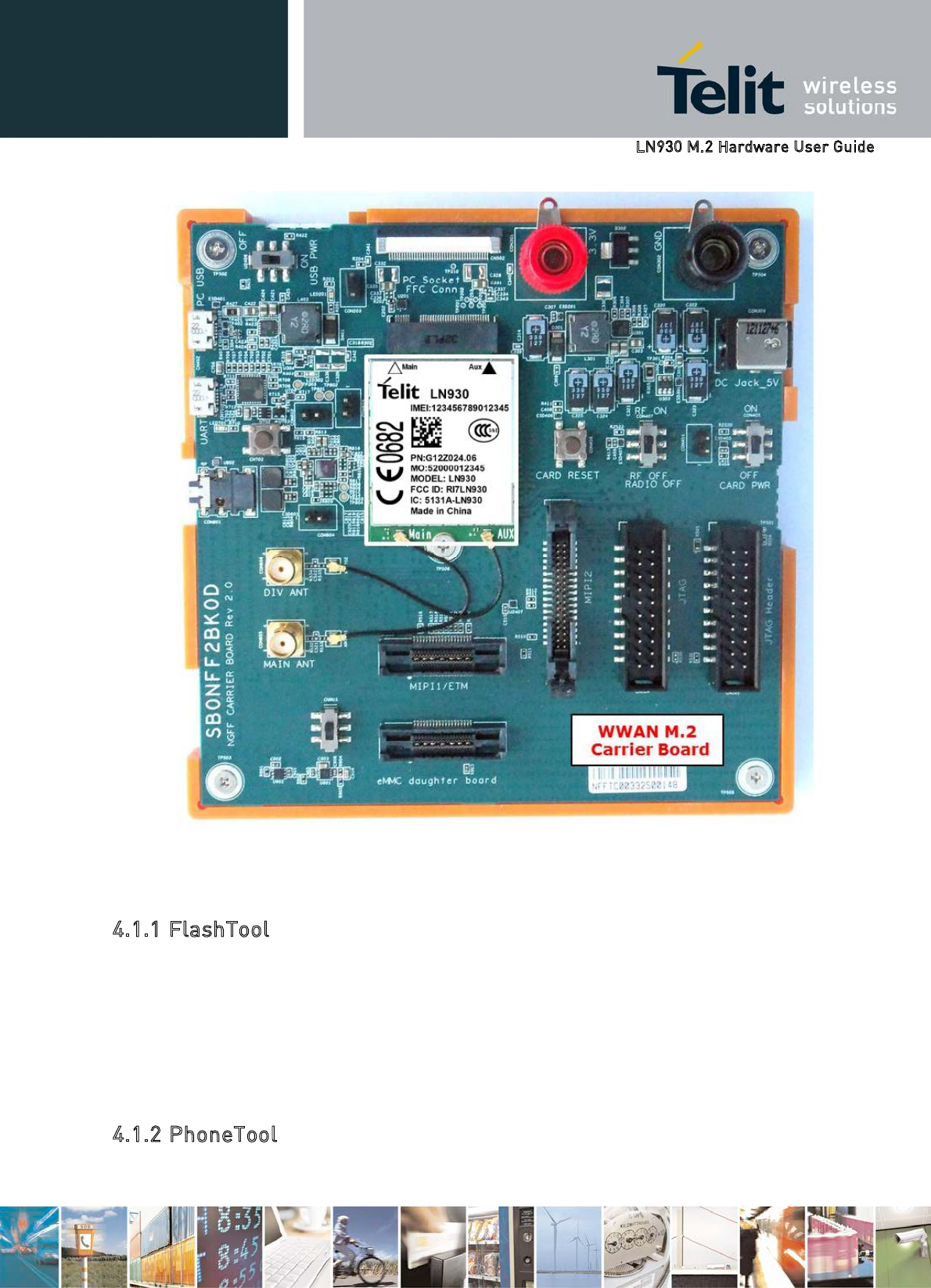
Figure 11 M.2 Carrier Board
Intel Mobile Communications provides a utility program called FlashTool for
downloading a binary image into the Flash memory of the M.2 module. The USB-HS port
or USIF on the platform is used for connection to a PC via a USB cable for flashing.
FlashTool is a Win32/64 application built on top of the dynamic link library,
Download.DLL.
PhoneTool is a development tool built on top of the so-called “production test dll,
DWDIO.dll”. PhoneTool can be used to fine tune the parameters of:
Audio configuration and settings (if enabled on M.2 module)
NV (Non-Volatile) memory
RF power ramp
Security data IMEI
SIM
Real Time Clock
It also includes interfaces for:
AT Terminal for sending and receiving AT commands.
DWDIO interface for manual access to the production test dll DWDIO.dll.
Generic Test Interface (GTI) for RF calibration.
System Trace Tool (STT) allows capturing trace sub-streams from different sources on
the platform in one combined stream.
Depending on the trace interface bandwidth, the combined data stream can be sent either
over one of the standard communication interfaces (e.g. USB) or over a dedicated high-
speed MIPI trace interface.
Captured trace data includes standard 3GPP IPC messages, print statements inserted by
developers in the code, error messages, and core dump (crash) information. The actual
decoding of the trace data is done by pluggable decoder libraries, DLL’s and scripts,
which are specific to the version of the mobile station software from which the trace is
captured.
The STT application has a GUI (Graphical User Interface) which provides an easy to use
graphical interface to view, search and analyze trace data. It supports advanced message
filtering runs on all Microsoft Windows® platforms.
STT will become the only tool for trace analysis in the future, the legacy trace tools,
Mobile Analyser and Artemis, will be continue to be supported for the 2G/3G WWAN
M.2 HSPA+ module.
XMMCalTool is a utility program that can be used for RF calibration. XMMCalTool
supports the following features:
Optimized calibration
3G TX closed loop power control
Parallel calibration 2G low/high band
Non-signaling verification
Industry leading fast sequenced test concept
Supports parallel RX and TX verification

Proven Single-Ended BER for faster BER
< 4 sec/per channel for 3G fast verification (BER, RSSI, TX, ILPC)
Tester supported: R&S CMU200, CMW500, and Agilent 8960
M.2 modules are marketed for use on Tablet, Ultrabook, and Laptop devices. OEM
vendors routinely offer multiple hardware configurations for the same base model, with
different processor speed, drive type, or display type, etc. Each configuration has a
different Radio Frequency emission profile with the possibility of introducing new
interference sources to a modem module.
The Noise Profiling Tool will measure, record down & plot graph of the RF noise level
present on each RX channel. This SW tool will switch on receiver port and sweep all
applicable RX channels on each band and each technology (WiFi, Bluetooth, GPS, and
GLONASS). This will allow OEM vendors to quickly know the noise jamming profile to the
modem module plugged in their devices.