Jorjin Technologies WG1300E00 Wireless LAN EM board for Module (802.11 bg) User Manual CC3000 WG1300E00 UG R01 20120302
Jorjin Technologies Inc. Wireless LAN EM board for Module (802.11 bg) CC3000 WG1300E00 UG R01 20120302
Contents
- 1. User Manual
- 2. User Manual - Statements
User Manual

Copyright © JORJIN TECHNOLOGIES INC. 2012
http://WWW.JORJIN.COM.TW
CONFIDENTIAL
a module solution provider
WG1300-00 EM Board
User Guide
Revision 0.1

Doc No: WG1300-00 EM Board-UG-D01
Copyright © JORJIN TECHNOLOGIES INC. 2012
http://WWW.JORJIN.COM.TW
CONFIDENTIAL
Page 1
Index
1. INTRODUCTION…………………………………………………………………1
2. WG1300-00 EM BOARD ........................................................................................ 2
2.1. TOP SIDE ............................................................................................................. 2
2.2. BOTTOM SIDE .................................................................................................... 5
2.3. Hardware setup…………………………………………………………………7
2.4. Schematics……………………………………………………………………...8
2.5. Bill of Material (BOM)………………………………………………………...9
3. APPLICATION EXAMPLES………………………………………………...…10
4. HISTORY CHANGE ............................................................................................. 11
Doc No: WG1300-00 EM Board-UG-D01
Copyright © JORJIN TECHNOLOGIES INC. 2012
http://WWW.JORJIN.COM.TW
CONFIDENTIAL
Page 2
1. INTRODUCTION
The purpose of this user guide is to help user understanding how to use
WG1300-00 EM (Evaluation Module) board to complete hardware
setup for test to evaluate the performances of CC3000-WG1300-00 SiP
Module.
2. WG1300-00 EM BOARD
In the following sub-sections, it’ll divide into TOP and BOTTOM Side to
explain details on the key parts and its features.
2.1. TOP Side
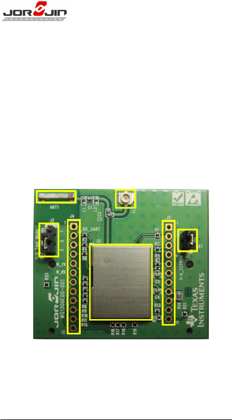
Figure 1 is TOP-Side picture of WG1300-00 EM Board.
Figure 1. TOP Side of WG1300-00 EM Board
The picture above marks some key parts and jumpers and Table 1
below shows the explanations to them in the details.
J3
J2 J5
J4 J1
Antenna
CC3000-WG1300-00
Module
Doc No: WG1300-00 EM Board-UG-D01
Copyright © JORJIN TECHNOLOGIES INC. 2012
http://WWW.JORJIN.COM.TW
CONFIDENTIAL
Page 3
Items Key Parts Descriptions
1
CC3000-WG1300-00
Module
The core module for performance evaluation. It’s
related feature can be referred to its datasheet.
2 Antenna It can used for radiated test by reworking cpacitor
to correct pads.
3 J1 It’s a U.FL RF connector via which you can proceed
conducted power test.
4
J2
It is a jumper via which we can swap testing modes,
test mode and operation mode. When pin 2 and
pin 3 are shorted, it runs in operation mode and it
operate in test mode when pin 1 and pin 2 are
shorted.
5
J3
It is a jumper for testing power consumption. In
operation mode, pins of the jumper is shorted. For
power testing, the jumper is removed and ammeter
crosses the pins to do the testing.
6 J4 Refer to Table 2. For more details on these
through-hole test points
7 J5 Refer to Table 3. For more details on these
through-hole test points
Table 1. TOP-Side Key parts of WG1300-00 EM Board
Table 2 below shows the signal descriptions of J4
Pin
Number Pin Name Pin Type Descriptions
1 GND Ground
2 NS_UARTD I/O Networking subsystem UART Debug line
3 FUNC4 -- Leave floating
4 WL_UART_DBG I/O UART Debug Line
5 WL_RS232_TX O Test RS232 transmit output; Leave floating
for normal operation
6 WL_RS232_RX I Test RS232 receive output; Leave floating
Doc No: WG1300-00 EM Board-UG-D01
Copyright © JORJIN TECHNOLOGIES INC. 2012
http://WWW.JORJIN.COM.TW
CONFIDENTIAL
Page 4
for normal operation
7 GND Ground
8 WL_SPI_CS I Host interface SPI Chip Select
9 WL_SPI_DOUT O Host interface SPI Data Ouput
10 WL_SPI_IRQ O Host Interface SPI Interrupt Request
11 WL_SPI_DIN I Host Interface SPI Data Input
12 WL_SPI_CLK I Host interface SPI Clock input
Table 2. TOP-Side J4 of WG1300-00 EM Board
Table 3 below shows the signal descriptions of J5
Pin
Number Pin Name Pin Type Descriptions
1
SCL_CC3000
O
I2C Clock signal output from CC3000. This
pin is connected to SCL_EEPROM via a
0-Ohm resister and is not used by end
users.
2
SCL_EEPROM
I
I2C Clock signal input from EEPROM inside
CC3000-WG1300-00 SiP Module. This pin is
connected to SCL_CC3000 via a 0-Ohm
resister and is not used by end users.
3
SDA_CC3000
I/O
I2C Data signal from CC3000. This pin is
connected to SDA_EEPROM via a 0-Ohm
resister and is not used by end users.
4
SDA_EEPROM
I/O
I2C Data signal from EEPROM inside
CC3000-WG1300-00 SiP Module. This pin is
connected to SDA_CC3000 via a 0-Ohm
resister and is not used by end users.
5 VBAT_SW_EN I Active-high enable signal from Host
device.
6 GND Ground
7 GND Ground
8
VIO_HOST
PI
VIO power supply from HOST to Module.
For MSP430 Host platform,
VIO_HOST=VBAT_IN. For other platforms
which have different voltage levels from
Doc No: WG1300-00 EM Board-UG-D01
Copyright © JORJIN TECHNOLOGIES INC. 2012
http://WWW.JORJIN.COM.TW
CONFIDENTIAL
Page 5
Battery voltages’, R14 can be remove to
support such a case.
9
VBAT_IN
PI
Battery voltage input to Module. For
MSP430 Host platform, VIO_HOST=VBAT_IN.
For other platforms which have different
voltage levels from Battery voltages’, R14
can be remove to support such a case.
10 GND Ground
11
EXT_32KHz
I
External Slow Clock input from Host
device. It can be used for the SiP Module
inside which hasn’t slow clock source.
Table 3. TOP-Side J5 of WG1300-00 EM Board
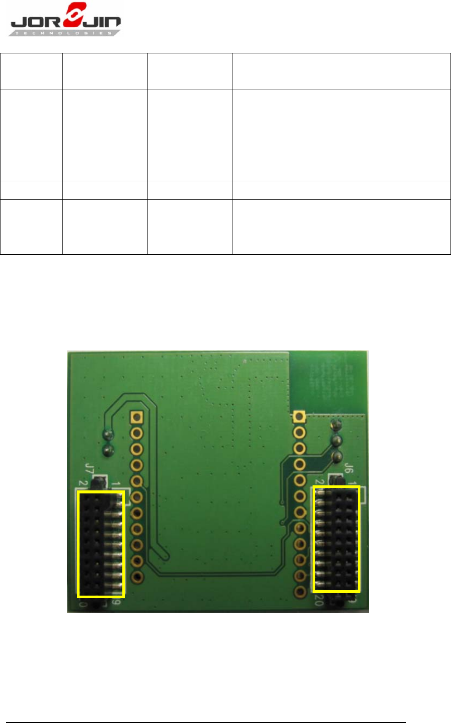
2.2. BOTTOM Side
Figure 2 is BOTTOM-Side picture of WG1300-00 EM Board.
Figure 2. Bottom Side of WG1300-00 EM Board
There are two EM Board mating connectors which are used for
connecting to Host platform and are mounted on the bottom side as
the picture above. Table 4 and Table 5 show the descriptions on the
J6 J7
Doc No: WG1300-00 EM Board-UG-D01
Copyright © JORJIN TECHNOLOGIES INC. 2012
http://WWW.JORJIN.COM.TW
CONFIDENTIAL
Page 6
signals brought out from these two EM mating connectors.
J6 Pin
Number
Pin Name Module Pin Type
Description
1 GND Ground
5
EXT_32KHz
I
External Slow Clock input from Host
device. It can be used for the SiP
Module inside which hasn’t slow clock
source.
10 VBAT_SW_EN I Active-high enable signal from Host
device.
12 WL_SPI_IRQ O Host Interface SPI Interrupt Request
14 WL_SPI_CS I Host interface SPI Chip Select
16 WL_SPI_CLK I Host interface SPI Clock input
18 WL_SPI_DIN I Host Interface SPI Data Input
19 GND Ground
20 WL_SPI_DOUT O Host interface SPI Data Ouput
Table 4. BOTTOM-Side J6 of WG1300-00 EM Board
J7 Pin
Number
Pin Name Module Pin Type
Description
2 GND Ground
7 VBAT_IN PI Battery voltage input to Module
9 VBAT_IN PI Battery voltage input to Module
15 EXT_32KHz I External Slow Clock input from Host
device.
Table 5. BOTTOM-Side J7 of WG1300-00 EM Board
Doc No: WG1300-00 EM Board-UG-D01
Copyright © JORJIN TECHNOLOGIES INC. 2012
http://WWW.JORJIN.COM.TW
CONFIDENTIAL
Page 7
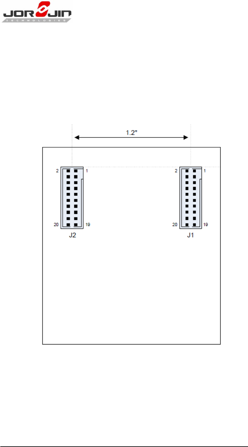
2.3. Hardware Setup
Before conducting performance test, EM Board should be connected
to Host platform, either with mating connectors, J6 and J7, or single
row headers, J4 and J5. For the case of using EM mating connector for
hardware connection, the mating EM connector should be lined up
and spaced 1.2” apart as Figure 3 below
Figure 3. Host PCB Mating Connector Arrangement
For the case of using single row headers, the necessary signals as the
ones brought out from EM mating connector need to be wired to Host
platform.
Doc No: WG1300-00 EM Board-UG-D01
Copyright © JORJIN TECHNOLOGIES INC. 2012
http://WWW.JORJIN.COM.TW
CONFIDENTIAL
Page 8
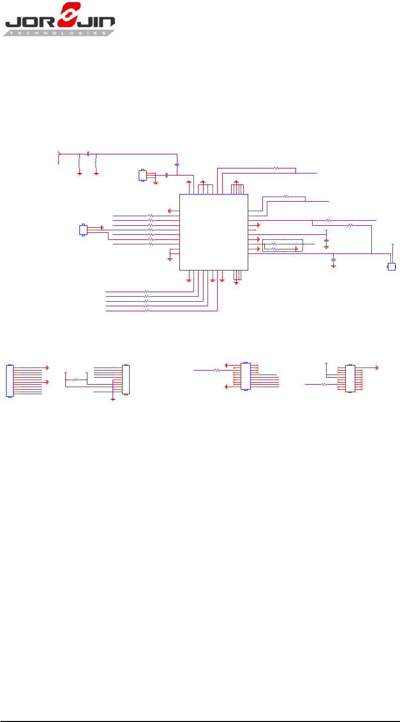
2.4. Schematics
Figure 4 is the schematics of WG1300-00 EM Board
R14 0R
RES1608
SCL_CC3000
EEPROM select:
Test mode => R1,R2 - NL
Functional mode => R1,R2 - 0R to short
VBAT_IN: 2.7V~4.8V => 3.3V TYP
VIO_HOST: Voltage of Host Level (1.2V~3.6V)
SCL_CC3000
SCL_EEPROM
SDA_CC300
SDA_EEPROM
VBAT_SW_EN
VIO_H OST
C3
10pF
CAP1005
J1
U.FL-R-SMT(10)
U.FL 1
2
3
L2
NL
IND1005
C1
10pF
CAP1005
L1
NL
IND1005 C2
NL_10pF
CAP1005
ANT1
AT8010
AT8010
1
2
VIO_HOST=VBAT_IN in MSP430 case
VBAT_IN
R21 0R
RES1005
EXT_32KHz
R1 0R RES1005
EXT_32KHz R20 0R
RES1005
C4
1uF
CAP1005
EXT_32KHz
VBAT_SW_EN
VBAT_IN
J3
HEADER 1x2
pitch 2.0-1x2
1
2
WL_RS232_TX
WL_RS232_RX
WL_SPI_CS
WL_SPI_DOUT
WL_SPI_IRQ
WL_SPI_DIN
WL_SPI_C LK
VBAT_IN
WG1300-00 Module
WL_SPI_CLK
WL_SPI_DIN
WL_SPI_IRQ
WL_SPI_DOUT
WL_SPI_CS
R190RRES1005
R170RRES1005
R150RRES1005
R160RRES1005
R180RRES1005
WL_SPI_CLK
WL_SPI_DIN
WL_SPI_IRQ
WL_SPI_DOUT
WL_SPI_CS
NS_UARTD
FUNC4
WL_UART_DBG
J4
NL_HEADER 1x12
pitch 2.0-1x12
1
2
3
4
5
6
7
8
9
10
11
12
SCL_EEPROM
Test mode => 1-2 short to GND
Functional mode => 2-3 short
R3 0R RES1005
R6 0R RES1005
R9 0R RES1005
R8 0R RES1005
R4 0R RES1005
R11 0R RES1005
R10 0R RES1005
NS_UARTD
FUNC4
WL_UART_DBG
WL_EN2
WL_RS232_TX
WL_RS232_RX
WL_EN1
J2
HEADER 1x 3
pitch 2.0-1x3
1
2
3
EM Connector
R12 NL_0R RES1005 EXT_32KHz
U1
WG1300-00
E-N46_13.5X16.3_TOP
WL_UART_DBG
4
NS_UARTD
2
WL_EN1
7
WL_EN2
5
FUNC4
3
WL_RS232_TX
6
WL_RS232_RX
8EXT_32K 21
GND 25
GND
9
SCL_CC3000 30
SCL_EEPROM 29
SDA_C C3000 28
SDA_EEPROM 27
GND 22
SPI_IRQ
14
SPI_DOUT
13
SPI_CS
12
SPI_CLK
17
SPI_DIN
15
VBAT_SW_EN 26
VBAT_IN 19
RF_ANT 35
GND 31
GND 33
GND
16
GND 34
VIO_H OST 23
GND 32
GND
37
GND
38
GND
39
GND
40
GND 41
GND 42
GND 43
GND 44
GND 46
GND 45
GND
1
GND
18
GND
10
GND 20
VIO_SOC 24
GND
11 GND 36
R5 0R RES1005 VBAT_SW_EN
R13 0R RES1005
R7 N L_1K RES1005
Internal 32kHz => R13 short to GND
External 32kHz => R12 short
VIO_H OST
J6
SFM-110-02-L-D-A
pitch 1.27-2x10
1
3
5
7
9
11
13
15
17
19
2
4
6
8
10
12
14
16
18
20
R2 0R RES1005
SDA_CC300
SDA_EEPROM
C5
1uF
CAP1005
J7
SFM-110-02-L-D-A
pitc h 1. 27-2x 10
1
3
5
7
9
11
13
15
17
19
2
4
6
8
10
12
14
16
18
20
Connect to RF1
Header for Debug
J5
NL_HEADER 1x11
pitc h 2. 0-1x11
1
2
3
4
5
6
7
8
9
10
11
Connect to RF2
Test mode => R7 - 1K to PU
Figure 4. Schematics of WG1300-00 EM Board
Doc No: WG1300-00 EM Board-UG-D01
Copyright © JORJIN TECHNOLOGIES INC. 2012
http://WWW.JORJIN.COM.TW
CONFIDENTIAL
Page 9
2.5. Bill Of Material (BOM)
Table 6. BOM of WG1300-00 EM Board
Items Reference Designator Description
1 U1 TI CC3000 WiFi b/g Module (BM)
2 ANT1 ANT / 2.4GHZ / Peak Gain 2.5DB
3 J1 Mini RF Header Receptacle
4 J2 CON Male 1x3 / Pitch 2.0 mm
5 J3 CON Male 1x2 / Pitch 2.0 mm
6 J6,J7 Female Header / Fool Proof H:4.3 / 2x10 /
Pitch 1.27mm / SMT
7 C1,C3 CAP 0402 / 10pF / 50V / NPO / ±5%
8 C4,C5 CAP 0402 / 1uF / X5R / 6.3V / ±10% / HF
9
R1,R2,R3,R4,R5,R6,R8,R9,
R10,R11,R13,R15,R16,
R17,R18,R19,R20,R21
RES 0402 / 0R / Jumper
10 R14 RES 0603 / 0R / Jumper
Doc No: WG1300-00 EM Board-UG-D01
Copyright © JORJIN TECHNOLOGIES INC. 2012
http://WWW.JORJIN.COM.TW
CONFIDENTIAL
Page 10
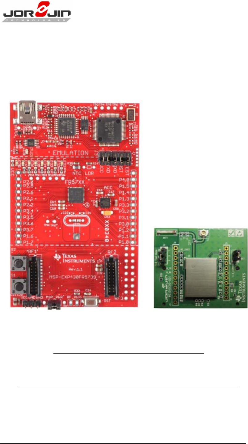
3. APPLICATION DEVELOPMENT
Texas Instrument had developed a HOST platform, MSP-EXP430FR5730,
for evaluating CC3000-based SiP Module. Figure 4 shows the platform
and WG1300-00 EM Board
Figure 4. MSP-EXP430FR5730 and WG1300-00 EM Board
The MSP-EXP430FR5739 test platform can be ordered as the link below.
http://www.ti.com/tool/msp-exp430fr5739
Specific application examples can refer to the link below
http://processors.wiki.ti.com/index.php/CC3000 Wi-Fi for MCU
Doc No: WG1300-00 EM Board-UG-D01
Copyright © JORJIN TECHNOLOGIES INC. 2012
http://WWW.JORJIN.COM.TW
CONFIDENTIAL
Page 11
4. HISTORY CHANGE
Revision Date Description
R 0.1 2012/2/28 Release 0.1