Laird Connectivity 60SIPT 802.11 ac/a/b/g/n + Bluetooth 4.2 module / 802.11 ac/a/b/g/n M.2 2230 + Bluetooth 4.2 module User Manual CS DS SU60 SIPT PRELIMINARY
Laird Technologies 802.11 ac/a/b/g/n + Bluetooth 4.2 module / 802.11 ac/a/b/g/n M.2 2230 + Bluetooth 4.2 module CS DS SU60 SIPT PRELIMINARY
Contents
- 1. Users Manual_60-2230C_SQG-60SIPT
- 2. Users Manual_60-SIPT_SQG-60SIPT
Users Manual_60-SIPT_SQG-60SIPT


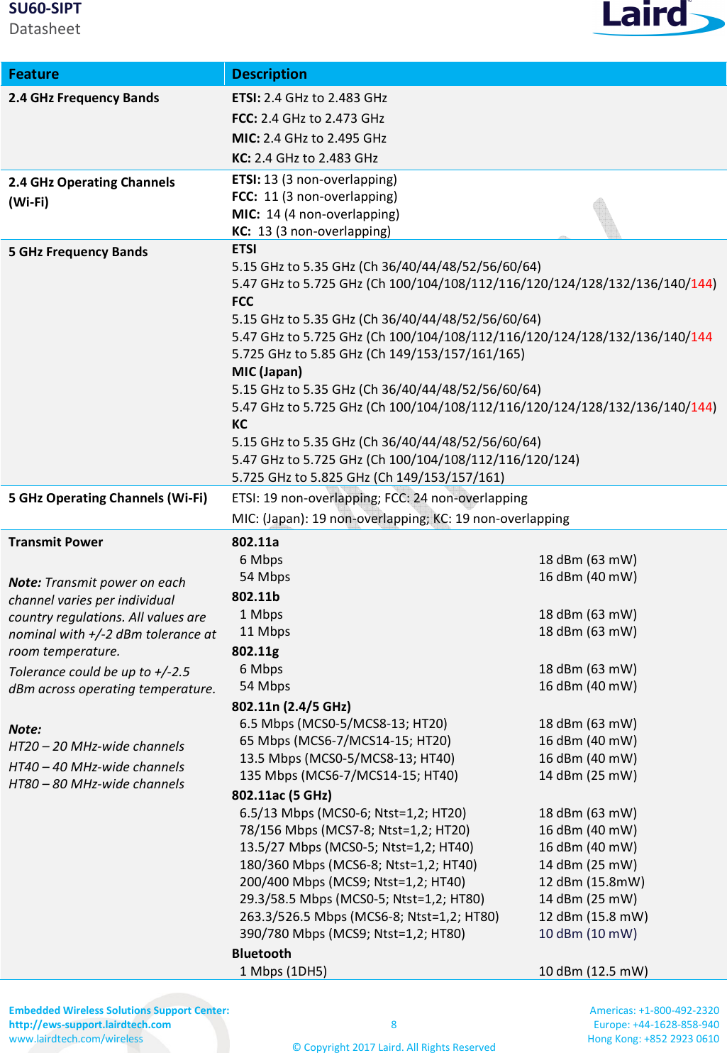
![SU60-SIPT Datasheet Embedded Wireless Solutions Support Center: http://ews-support.lairdtech.com www.lairdtech.com/wireless 5 © Copyright 2017 Laird. All Rights Reserved Americas: +1-800-492-2320 Europe: +44-1628-858-940 Hong Kong: +852 2923 0610 3 60-SIPT SERIES FEATURES SUMMARY The Laird 60-SIPT series device features are described in Table 2. Table 2: 60-SIPT series features Feature Description Radio Front End Integrates the complete transmit/receive RF paths including band pass filter, diplexer, switches, reference crystal oscillator, and power manage unit (PMU). Supports 20/40/80MHz channel bandwidth. WLAN/Bluetooth share one antenna. The Bluetooth® word mark and logos are registered trademarks owned by Bluetooth SIG, Inc. Any use of such marks by Laird is under license. Other trademarks and trade names are those of their respective owners. Coexistence Coexistence arbitration for WLAN, Bluetooth, and LTE operation Power Management Dynamic Voltage Scaling (DVS) and Adaptive Voltage Scaling (AVS) features support the latest Marvell SoC and Processor power control scheme. Pre-Calibration RF system tested and calibrated in production Sleep Clock An external sleep clock of 32.768 KHz is required during power save mode Host Interface SDIO 3.0 (4-bit and 1-bit), SDR 12/25/50 mode (up to 100 MHz), USB2.0 or PCIe for WLAN SDIO 3.0, USB 2.0, HS-UART for Bluetooth HCI (compatible with any upper layer Bluetooth stack) PCM digital audio interface for Bluetooth audio application Strap Value CONFIG_HOST [2-0] WLAN Bluetooth/BLE ROM Notes 000 SDIO UART - 001 SDIO SDIO - 010 PCIe USB 2.0 Initial USB 2.0 PHY and COM PHY PCIe portion 011 PCIe UART Initial only COM PHY PCIe portion 100 USB 2.0 UART Initial COM PHY USB 2.0 101 USB 2.0 USB 2.0 Initial only USB 2.0 PHY Reference Frequency Incorporates a 40 MHz reference frequency source in package An external sleep clock is recommended for minimal current consumption. If no sleep clock input is provided, an internal sleep clock (derived from reference clock) is used. An approximate 50 uA current increase on the 3.3V rail. Advanced WLAN A-MPDU RX (de-aggregation) and TX (aggregation) supports 802.11ac single-MPDU A-MPDU. Multi-BSS/Station Transmit rate adaption, transmit power control Modulation and coding scheme (MCS): 802.11ac—MCS0-9 Nsts=1 and 2. 802.11n—MCS0-15 Dynamic frequency selection (radar detection) DFS 20/40/80 MHz channel bandwidths support On-chip gain selectable LNA with optimized noise figure and power consumption Internal PA with optimized gain distribution for linearity and noise performance Support wide variety of WLAN encryption: TKIP/WEP/AES](https://usermanual.wiki/Laird-Connectivity/60SIPT.Users-Manual-60-SIPT-SQG-60SIPT/User-Guide-3490644-Page-5.png)
![SU60-SIPT Datasheet Embedded Wireless Solutions Support Center: http://ews-support.lairdtech.com www.lairdtech.com/wireless 6 © Copyright 2017 Laird. All Rights Reserved Americas: +1-800-492-2320 Europe: +44-1628-858-940 Hong Kong: +852 2923 0610 Feature Description Advanced Bluetooth Bluetooth 4.2 (BDR/EDR/LE), Bluetooth class 1 Support data rate: 1 Mbps(GFSK), 2 Mbps ( /4-DQPSK), 3 Mbps (8-DPSK) Digital audio interface with PCM/TDM interface for voice application Adaptive Frequency Hopping (AFH) using Package Error Rate (PER) Standard SDIO or UART HCI transport layer WLAN/Bluetooth coexistence protocol support Shared LNA with WLAN/Bluetooth Encryption (AES) support 4 SPECIFICATIONS Table 3: Specifications Feature Description Physical Interface 84-pin LGA package (including 16 thermal ground pad under the package) Wi-Fi Interface 1-bit or 4-bit Secure Digital I/O; PCIe v3.0 Gen1/Gen2 (2.5/5 Gbps); USB 2.0 Bluetooth/BLE Interface Host Controller Interface (HCI) using high speed UART, SDIO, USB 2.0 Strap Value CONFIG_HOST [2-0] WLAN Bluetooth/ BLE ROM Notes 000 SDIO UART - 001 SDIO SDIO - 010 PCIe USB 2.0 Initial USB 2.0 PHY and COM PHY PCIe portion 011 PCIe UART Initial only COM PHY PCIe portion 100 USB 2.0 UART Initial COM PHY USB 2.0 101 USB 2.0 USB 2.0 Initial only USB 2.0 PHY Main Chip Marvell 88W8997 (WLAN/BT); Marvell 88PG823 (PMU) Input Voltage Requirements DC 3.3 V ±10% I/O Signalling Voltage DC 3.3 V ± 10% or DC 1.8 V ± 10% Operating Temperature -30° to 85°C (-22° to 185°F) Operating Humidity 10 to 90% (non-condensing) Storage Temperature -40° to 85°C (-40° to 185°F) Storage Humidity 10 to 90% (non-condensing) Maximum Electrostatic Discharge Conductive 4KV; Air coupled 8KV follow EN61000-4-2 Size 13 mm (length) x 14 mm (width) x 1.87 mm (thickness) Weight TBD g Wi-Fi Media Direct Sequence-Spread Spectrum (DSSS) Complementary Code Keying (CCK) Orthogonal Frequency Divisional Multiplexing (OFDM) Bluetooth Media Frequency Hopping Spread Spectrum (FHSS) Wi-Fi Media Access Protocol Carrier sense multiple access with collision avoidance (CSMA/CA) A-MPDU Rx (De-aggregation) and Tx (aggregation) (802.11ac single-MPDU A-MPDU) Network Architecture Types Infrastructure and ad-hoc](https://usermanual.wiki/Laird-Connectivity/60SIPT.Users-Manual-60-SIPT-SQG-60SIPT/User-Guide-3490644-Page-6.png)


![SU60-SIPT Datasheet Embedded Wireless Solutions Support Center: http://ews-support.lairdtech.com www.lairdtech.com/wireless 19 © Copyright 2017 Laird. All Rights Reserved Americas: +1-800-492-2320 Europe: +44-1628-858-940 Hong Kong: +852 2923 0610 Symbol Parameter Conditions Min Typ Max Unit 11ac HT80 mask compliant MCS0-5 (Ntst=1,2) 14 11ac HT80 EVM compliant MCS6-8(Ntst=1,2) 12 11ac HT80 EVM compliant MCS9(Ntst=1,2) 10 ATx Transmit power accuracy at 25 - -2.0 - +2.0 dB Table 15: WLAN current consumption on 5 GHz Freq. Mode/Rate [Mbps] Output Power Per Chain [dBm] Typical Current Consumption Single Chain (mA) Typical Current Consumption Dual Chain (mA) 5180 MHz 5190 MHz 6 Mbps 18 dBm 400 710 54 Mbps 16 dBm 330 610 HT20 MCS0 18 dBm 400 720 HT20 MCS7 16 dBm 360 620 HT40 MCS7 14 dBm 320 550 5500 MHz 5510 MHz 6 Mbps 18 dBm 380 680 54 Mbps 16 dBm 330 600 HT20 MCS0 18 dBm 370 690 HT20 MCS7 16 dBm 320 600 HT40 MCS7 14 dBm 300 530 5825 MHz 5795 MHz 6 Mbps 18 dBm 380 690 54 Mbps 16 dBm 310 600 HT20 MCS0 18 dBm 360 710 HT20 MCS7 16 dBm 340 550 HT40 MCS7 14 dBm 300 530 Note: Final TX power values on each channel are limited by the regulatory certification test limit. 9 BLUETOOTH RADIO CHARACTERISTICS Table 16 through Table 17 describe the basic rate transmitter performance, enhanced data transmitter performance, basic rate receiver performance, enhanced rate receiver performance, and current consumption conditions at 25°C. Table 16: Basic rate transmitter performance temperature at 25°C (3.3V) Test Parameter Min Typ Max BT Spec. Unit Maximum RF Output Power 8 10 11 0 ~ +20 dBm Frequency Range 2.4 — 2.4835 2.4 ≤ f ≤ 2.4835 GHz 20 dB Bandwidth — 919.5 — ≤ 1000 KHz Δf1avg Maximum Modulation 140 165 175 140 < Δf1avg < 175 KHz Δf2max Minimum Modulation — 135 — ≥ 115 KHz Δf2avg/Δf1avg — 0.9 — ≥ 0.80 —](https://usermanual.wiki/Laird-Connectivity/60SIPT.Users-Manual-60-SIPT-SQG-60SIPT/User-Guide-3490644-Page-19.png)

![SU60-SIPT Datasheet Embedded Wireless Solutions Support Center: http://ews-support.lairdtech.com www.lairdtech.com/wireless 25 © Copyright 2017 Laird. All Rights Reserved Americas: +1-800-492-2320 Europe: +44-1628-858-940 Hong Kong: +852 2923 0610 10.1.4 DDR50 Mode (50MHz) (1.8V) Figure 6: SDIO CMD timing diagram--- DDR50 modes (50 MHz) (1.8V) Figure 7: SDIO DAT[3:0] timing Diagram--- DDR50 modes (50 MHz) (1.8V) Note: In DDR50 mode, DAT[3:0] lines are samples on both edges pf the clock (not applicable for CMD line) Table 23: SDIO timing requirements – DDR50 modes (50 MHz) Symbol Parameter Condition Min. Typ. Max. Unit Clock TCLK Clock time 50MHz (max) between rising edge DDR50 20 -- -- ns TCR, TCF Rise time, fall time TCR, TCF <4.00ns (max) at 50MHz. CCARD=10pF DDR50 -- -- 0.2*TCLK ns Clock Duty -- DDR50 45 -- 55 % CMD Input (referenced to clock rising edge) TIS Input setup time CCARD DDR50 6 -- -- ns](https://usermanual.wiki/Laird-Connectivity/60SIPT.Users-Manual-60-SIPT-SQG-60SIPT/User-Guide-3490644-Page-25.png)
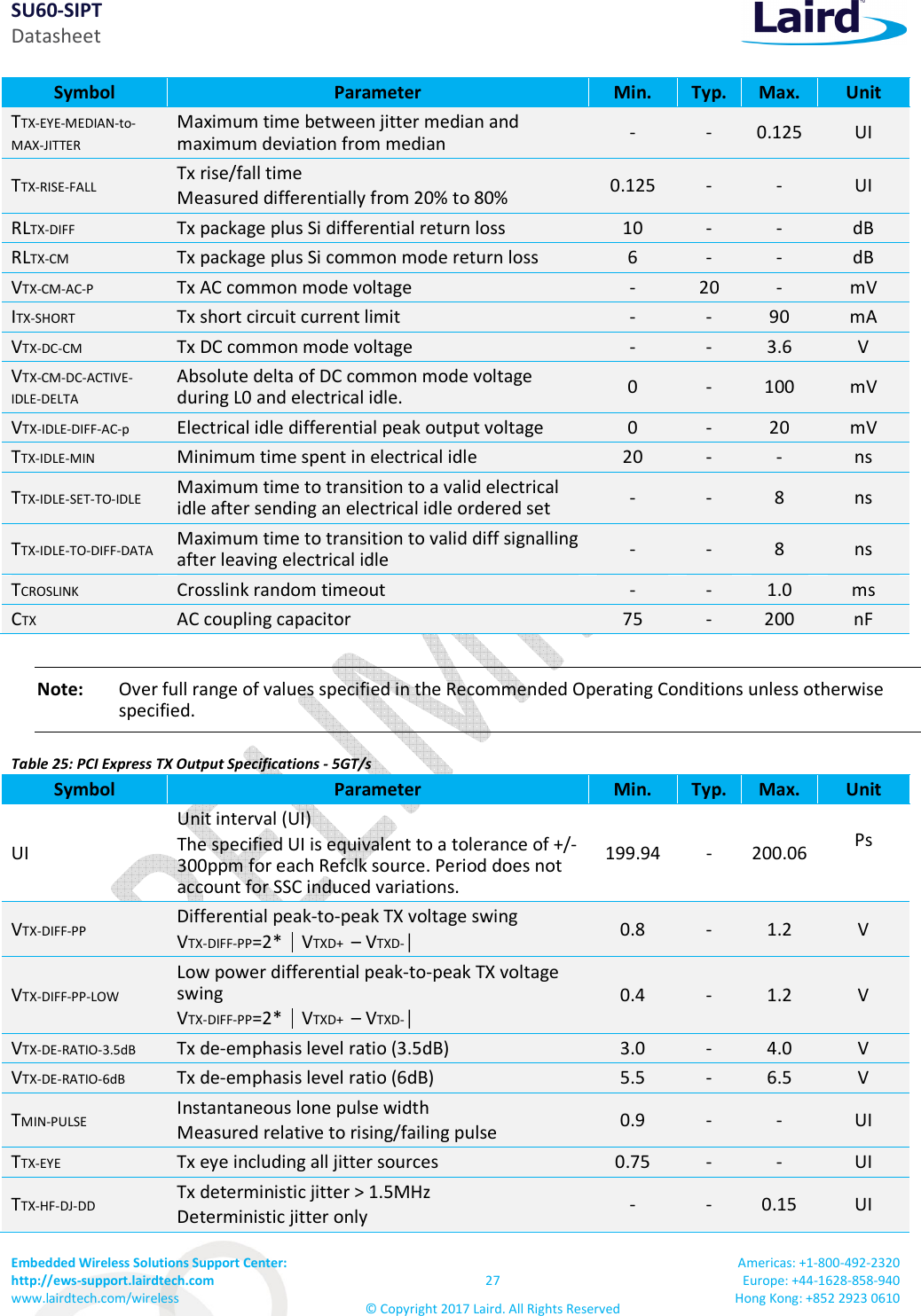
![SU60-SIPT Datasheet Embedded Wireless Solutions Support Center: http://ews-support.lairdtech.com www.lairdtech.com/wireless 26 © Copyright 2017 Laird. All Rights Reserved Americas: +1-800-492-2320 Europe: +44-1628-858-940 Hong Kong: +852 2923 0610 Symbol Parameter Condition Min. Typ. Max. Unit TIH Input hold time CCARD DDR50 0.8 -- -- ns CMD Output (referenced to clock rising and failing edge) TODLY Output delay time during data transfer mode CL30pF (1 card) DDR50 -- -- 13.7 ns TOHLD Output hold time CL≥15pF (1 card) DDR50 1.5 -- -- ns DAT[3:0] Input (referenced to clock rising and failing edges) TIS2X Input setup time CCARD DDR50 3 -- -- ns TIH2X Input hold time CCARD DDR50 0.8 -- -- ns DAT[3:0] Output (referenced to clock rising and failing edges) TODLY2X (max) Output delay time during data transfer mode CL25pF (1 card) DDR50 -- -- 7.0 ns TODLY2X (min) Output hold time CL≥15pF (1 card)) DDR50 1.5 -- -- ns 10.2 PCI Express Specifications The PCI Express host interface pins are powered from the 1.8V generated by the PMU inside the 60-SIPT series. 10.2.1 Differential TX Output Electricals Note: Over full range of values specified in the Recommended Operating Conditions unless otherwise specified. Table 24: PCI Express TX Output Specifications – 2.5GT/s Symbol Parameter Min. Typ. Max. Unit UI Unit interval (UI) The specified UI is equivalent to a tolerance of +/-300ppm for each Refclk source. Period does not account for SSC induced variations. 399.88 - 400.12 Ps VTX-DIFF-PP Differential peak-to-peak TX voltage swing VTX-DIFF-PP=2* VTXD+ – VTXD-│ 0.8 - 1.2 V VTX-DIFF-PP-LOW Low power differential peak-to-peak TX voltage swing VTX-DIFF-PP=2* VTXD+ – VTXD-│ 0.4 - 1.2 V VTX-DE-RATIO-3.5dB Tx de-emphasis level ratio (3.5dB) 3.0 - 4.0 V TTX-EYE Tx eye including all jitter sources 0.75 - - UI](https://usermanual.wiki/Laird-Connectivity/60SIPT.Users-Manual-60-SIPT-SQG-60SIPT/User-Guide-3490644-Page-26.png)

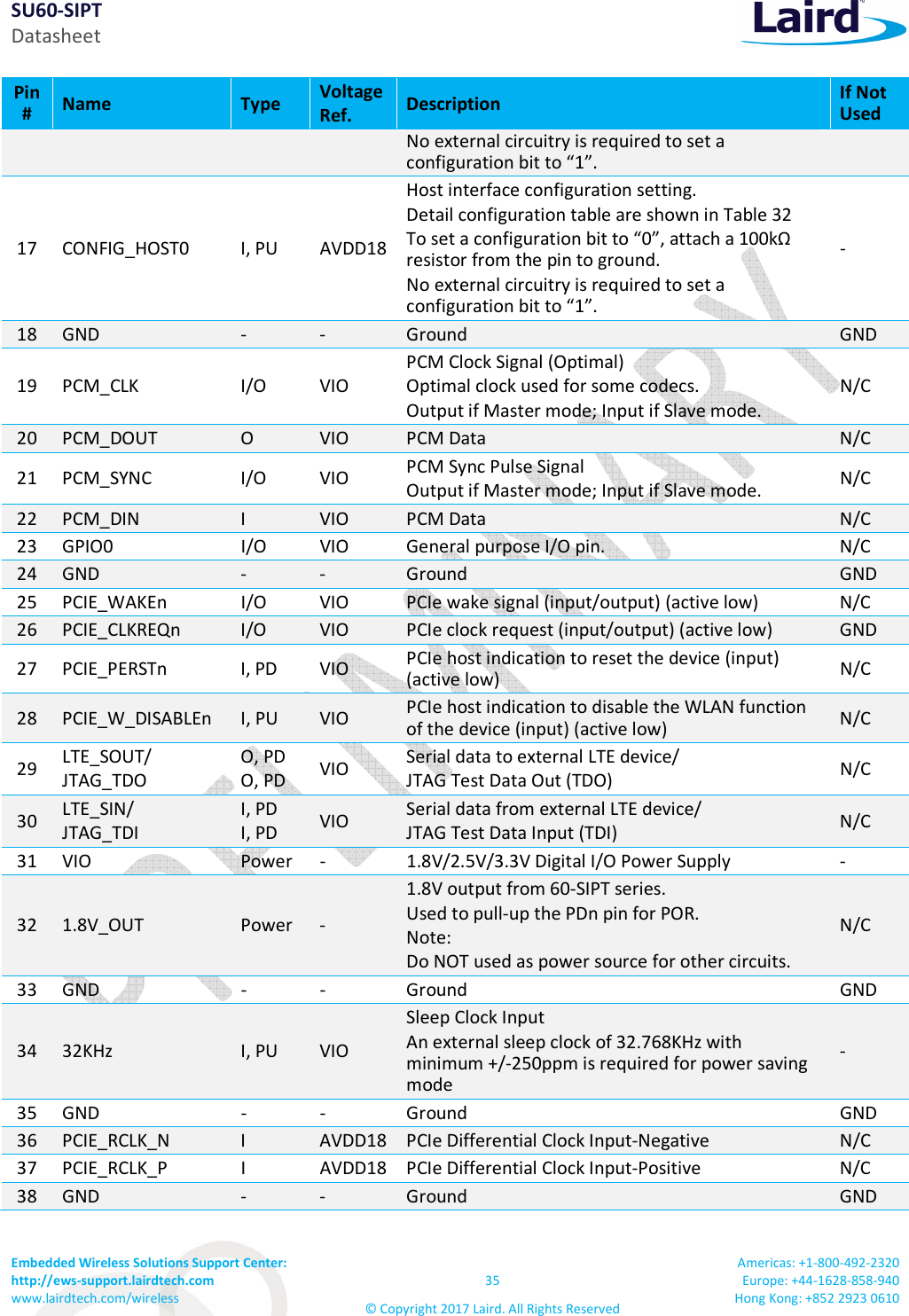
![SU60-SIPT Datasheet Embedded Wireless Solutions Support Center: http://ews-support.lairdtech.com www.lairdtech.com/wireless 36 © Copyright 2017 Laird. All Rights Reserved Americas: +1-800-492-2320 Europe: +44-1628-858-940 Hong Kong: +852 2923 0610 Pin # Name Type Voltage Ref. Description If Not Used 39 PCIE_TX_P O AVDD18 PCIe Transmit Data-Positive N/C 40 PCIE_TX_N O AVDD18 PCIe Transmit Data-Negative N/C 41 GND - - Ground GND 42 PCIE_RX_N I AVDD18 PCIe Receive Data-Negative N/C 43 PCIE_RX_P I AVDD18 PCIe Receive Data-Positive N/C 44 GND - - Ground GND 45 USB_DN I/O 3V3 USB Differential Data-Negative N/C 46 USB_DP I/O 3V3 USB Differential Data-Positive N/C 47 GND - - Ground GND 48 3V3 Power - 3.3V module power supply Note: A 10u MLCC is needed for this pin. Place the capacitor close to this pin as possible. Ref. parts: GRM188R60J106ME47D (MURATA) or CC0805KKX7R6BB106 (YAGO) - 49 3V3 Power - 3.3V module power supply Note: A 10u MLCC is needed for this pin. Place the capacitor close to this pin as possible. Ref. parts: GRM188R60J106ME47D (MURATA) or CC0805KKX7R6BB106 (YAGO) - 50 GND - - Ground GND 51 PMU_EN I Enable input for all Regulators inside the 60-SIPT series when it is “H” state. The 60-SIPT will be off when it is “L” state. Note: DO NOT float this pin. Pull-up to 3.3V with 100K for normal operation. 100K, PU 52 VIO_SD Power - 1.8V/3.3V Digital I/O SDIO Power Supply - 53 SDIO_DATA0 I/O, PU VIO_SD SDIO 4-bit Mode DATA line Bit[0] N/C 54 SDIO_DATA1 I/O, PU VIO_SD SDIO 4-bit Mode DATA line Bit[1] N/C 55 SDIO_DATA2 I/O, PU VIO_SD SDIO 4-bit Mode DATA line Bit[2] N/C 56 SDIO_DATA3 I/O, PU VIO_SD SDIO 4-bit Mode DATA line Bit[3] N/C 57 SDIO_CMD I/O, PU VIO_SD SDIO 4-bit Mode Command/Response N/C 58 SDIO_CLK I, PU VIO_SD SDIO 4-bit Mode Clock Input N/C 59 GND - - Ground GND 60 UART_TXD O, WPU VIO UART Serial Data Output N/C 61 UART_RXD I, WPU VIO UART Serial Data Input N/C 62 UART_CTSn I, PU VIO UART Clear to Send (Active low) N/C 63 UART_RTSn O, WPU VIO UART Request to Send (Active low) N/C 64 GND - - Ground GND 65 JTAG_TCK I, PU VIO JTAG Test Clock (input) N/C 66 JTAG_TMS I, PU VIO JTAG Test Controller Select (input) N/C](https://usermanual.wiki/Laird-Connectivity/60SIPT.Users-Manual-60-SIPT-SQG-60SIPT/User-Guide-3490644-Page-36.png)
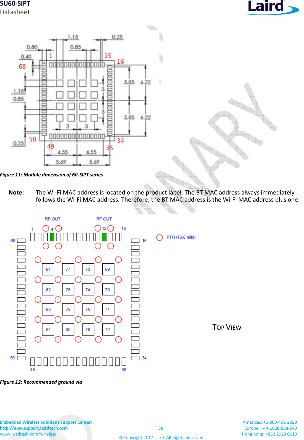
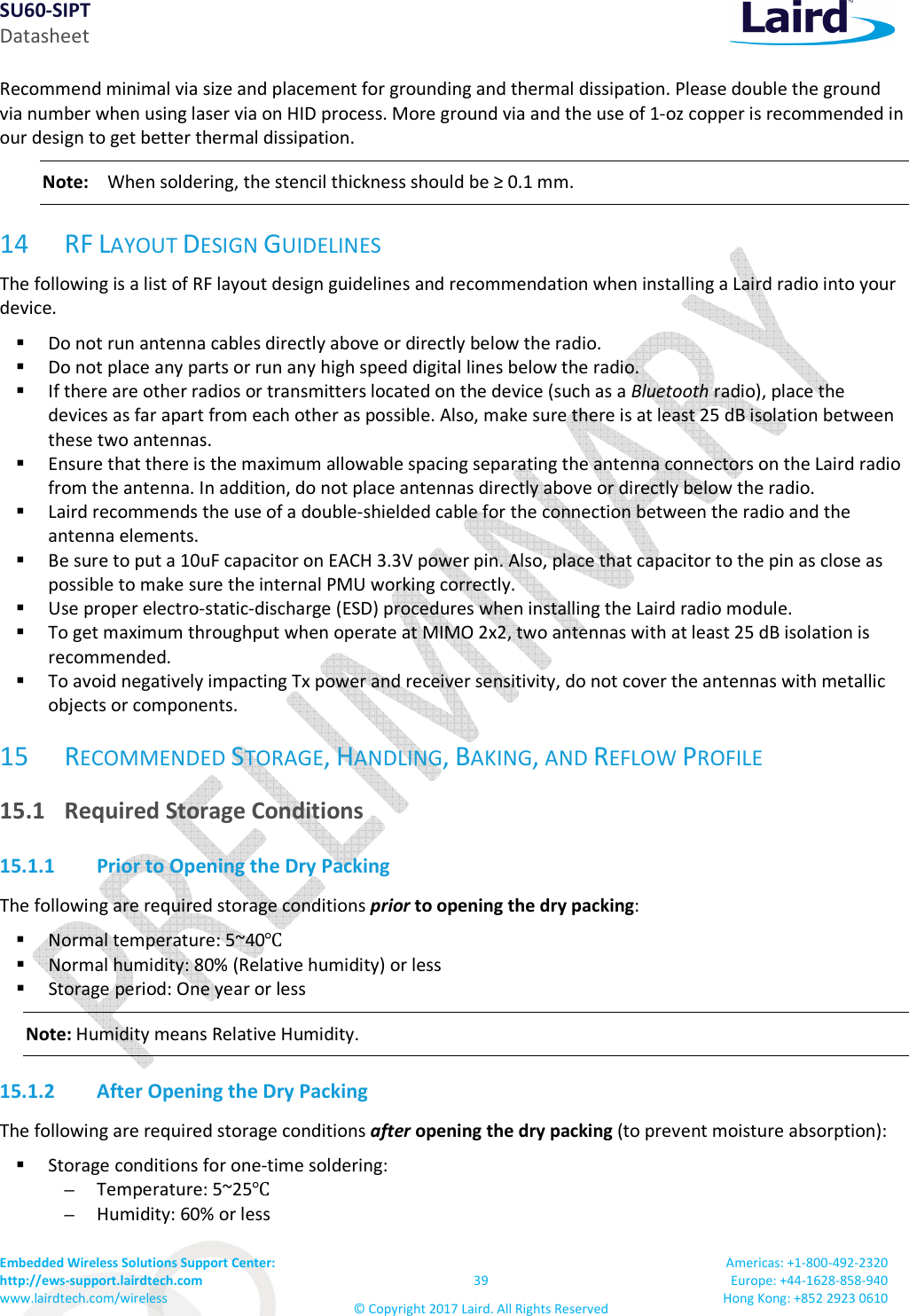
![SU60-SIPT Datasheet Embedded Wireless Solutions Support Center: http://ews-support.lairdtech.com www.lairdtech.com/wireless 37 © Copyright 2017 Laird. All Rights Reserved Americas: +1-800-492-2320 Europe: +44-1628-858-940 Hong Kong: +852 2923 0610 Pin # Name Type Voltage Ref. Description If Not Used 67 LED_OUT_BT O, PU VIO LED indicator for BT with 10mA drive capability. N/C 68 LED_OUT_WLAN O, PU VIO LED indicator for WLAN with 10mA drive capability N/C 69-84 GND - - Thermal Ground Pad (Important for RF performance and thermal dissipation; please flow the reference design) GND 12 HOST CONFIGURATION OPTIONS 60-SIPT series support various host configurations for WLAN and BT. Its detail configurations are shown in following table (Error! Reference source not found.). Table 34: Wi-Fi host interface configuration table CONFIG_HOST [2-0] WLAN BT/BLE Note 000 SDIO UART - 001 SDIO SDIO - 010 PCIe USB 2.0 Initial USB 2.0 PHY and COM PHY PCIe portion 011 PCIe UART Initial only COM PHY PCIe portion 100 USB 2.0 UART Initial USB 2.0 PHY 101 USB 2.0 USB 2.0 Initial only USB 2.0 PHY 13 MECHANICAL SPECIFICATIONS Module dimensions of 60-SIPT series is 13 x 14 x 1.87 mm. Detail drawings are shown in Figure 10. Figure 10: Mechanical drawing - 60-SIPT](https://usermanual.wiki/Laird-Connectivity/60SIPT.Users-Manual-60-SIPT-SQG-60SIPT/User-Guide-3490644-Page-37.png)

![SU60-SIPT Datasheet Embedded Wireless Solutions Support Center: http://ews-support.lairdtech.com www.lairdtech.com/wireless 49 © Copyright 2017 Laird. All Rights Reserved Americas: +1-800-492-2320 Europe: +44-1628-858-940 Hong Kong: +852 2923 0610 tel: +1-262-375-4400 fax: +1-262-364-2649 Date of Issue: May 2017 Name of Authorized Person: Thomas T Smith, Director of EMC Compliance Signature of Authorized Person: Maximum Output Power for Each Frequency TBD 20.5 dBm, 5.15-5.25 GHz 20.5 dBm, 5.25-5.35 GHz 20.5 dBm, 5.47-5.725 GHz Software Version for Testing SW version: P95 The minimum distance between the user and/or any bystander and the radiating structure of the transmitter is 20 cm. 5150 ~ 5350 MHz is limited to indoor used in the following countries: BE DK IE FR CY LU NL PT SK UK NO BG DE EL HR LV HU AT RO FI LI TR CZ EE ES IT LT MT PL SI SE IS CH 19 ORDERING INFORMATION Part Number Description 60-SIPT series 2X2 802.11 a/b/g/n/ac with BT4.2 dual mode module. 19.1 General Comments This is a preliminary datasheet. Please check with Laird for the latest information before commencing a design. If in doubt, ask. Česky [Czech] [Jméno výrobce] tímto prohlašuje, že tento [typ zařízení] je ve shodě se základními požadavky a dalšími příslušnými ustanoveními směrnice 1999/5/ES. Dansk [Danish] Undertegnede [fabrikantens navn] erklærer herved, at følgende udstyr [udstyrets typebetegnelse] overholder de væsentlige krav og øvrige relevante krav i direktiv 1999/5/EF. Deutsch [German] Hiermit erklärt [Name des Herstellers], dass sich das Gerät [Gerätetyp] in Übereinstimmung mit den grundlegenden Anforderungen und den übrigen einschlägigen Bestimmungen der Richtlinie 1999/5/EG befindet. Eesti [Estonian] Käesolevaga kinnitab [tootja nimi = name of manufacturer] seadme [seadme tüüp = type of equipment] vastavust direktiivi 1999/5/EÜ põhinõuetele ja nimetatud direktiivist tulenevatele teistele asjakohastele sätetele. English Hereby, [name of manufacturer], declares that this [type of equipment] is in compliance with the essential requirements and other relevant provisions of Directive 1999/5/EC. Español [Spanish] Por medio de la presente [nombre del fabricante] declara que el [clase de equipo] cumple con los requisitos esenciales y cualesquiera otras disposiciones aplicables o exigibles de la Directiva 1999/5/CE.](https://usermanual.wiki/Laird-Connectivity/60SIPT.Users-Manual-60-SIPT-SQG-60SIPT/User-Guide-3490644-Page-49.png)
![SU60-SIPT Datasheet Embedded Wireless Solutions Support Center: http://ews-support.lairdtech.com www.lairdtech.com/wireless 50 © Copyright 2017 Laird. All Rights Reserved Americas: +1-800-492-2320 Europe: +44-1628-858-940 Hong Kong: +852 2923 0610 Ελληνική [Greek] ΜΕ ΤΗΝ ΠΑΡΟΥΣΑ [name of manufacturer] ∆ΗΛΩΝΕΙ ΟΤΙ [type of equipment] ΣΥΜΜΟΡΦΩΝΕΤΑΙ ΠΡΟΣ ΤΙΣ ΟΥΣΙΩ∆ΕΙΣ ΑΠΑΙΤΗΣΕΙΣ ΚΑΙ ΤΙΣ ΛΟΙΠΕΣ ΣΧΕΤΙΚΕΣ ∆ΙΑΤΑΞΕΙΣ ΤΗΣ Ο∆ΗΓΙΑΣ 1999/5/ΕΚ. Français [French] Par la présente [nom du fabricant] déclare que l'appareil [type d'appareil] est conforme aux exigences essentielles et aux autres dispositions pertinentes de la directive 1999/5/CE. Italiano [Italian] Con la presente [nome del costruttore] dichiara che questo [tipo di apparecchio] è conforme ai requisiti essenziali ed alle altre disposizioni pertinenti stabilite dalla direttiva 1999/5/CE. Latviski [Latvian] Aršo[name of manufacturer /izgatavotājanosaukums] deklarē, ka[type of equipment / iekārtas tips]atbilstDirektīvas 1999/5/EK būtiskajāmprasībām un citiemar to saistītajiemnoteikumiem. Lietuvių [Lithuanian] Šiuo [manufacturer name] deklaruoja, kad šis [equipment type] atitinka esminius reikalavimus ir kitas 1999/5/EB Direktyvos nuostatas. Nederlands [Dutch] Hierbij verklaart [naam van de fabrikant] dat het toestel [type van toestel] in overeenstemming is met de essentiële eisen en de andere relevante bepalingen van richtlijn 1999/5/EG. Malti [Maltese] Hawnhekk, [isem tal-manifattur], jiddikjara li dan [il-mudel tal-prodott] jikkonforma mal-ħtiġijiet essenzjali u ma provvedimenti oħrajn relevanti li hemm fid-Dirrettiva 1999/5/EC. Magyar [Hungarian] Alulírott, [gyártó neve] nyilatkozom, hogy a [... típus]megfelel a vonatkozó alapvetõ követelményeknek és az 1999/5/EC irányelv egyéb elõírásainak. Polski [Polish] Niniejszym [nazwa producenta] oświadcza, że [nazwa wyrobu] jest zgodny z zasadniczymi wymogami oraz pozostałymi stosownymi postanowieniami Dyrektywy 1999/5/EC. Português [Portuguese] [Nome do fabricante] declara que este [tipo de equipamento] está conforme com os requisitos essenciais e outras disposições da Directiva 1999/5/CE. Slovensko [Slovenian] [Ime proizvajalca] izjavlja, da je ta [tip opreme] v skladu z bistvenimi zahtevami in ostalimi relevantnimi določili direktive 1999/5/ES. Slovensky [Slovak] [Menovýrobcu]týmtovyhlasuje, že[typzariadenia]spĺňazákladnépožiadavky a všetkypríslušnéustanoveniaSmernice 1999/5/ES. Suomi [Finnish] [Valmistaja = manufacturer] vakuuttaa täten että [type of equipment = laitteen tyyppimerkintä] tyyppinen laite on direktiivin 1999/5/EY oleellisten vaatimusten ja sitä koskevien direktiivin muiden ehtojen mukainen. Svenska [Swedish] Härmed intygar [företag] att denna [utrustningstyp] står I överensstämmelse med de väsentliga egenskapskrav och övriga relevanta bestämmelser som framgår av direktiv 1999/5/EG. 19.1.1 Labeling Requirements The end product must be labeled in a visible area with the following notice: © Copyright 2017 Laird. All Rights Reserved. Any information furnished by Laird and its agents is believed to be accurate and reliable. All specifications are subject to change without notice. Responsibility for the use and application of Laird materials or products rests with the end user since Laird and its agents cannot be aware of all potential uses. Laird makes no warranties as to non-infringement nor as to the fitness, merchantability, or sustainability of any Laird materials or products for any specific or general uses. Laird, Laird Technologies, Inc., or any of its affiliates or agents shall not be liable for incidental or consequential damages of any kind. All Laird products are sold pursuant to the Laird Terms and Conditions of Sale in effect from time to time, a copy of](https://usermanual.wiki/Laird-Connectivity/60SIPT.Users-Manual-60-SIPT-SQG-60SIPT/User-Guide-3490644-Page-50.png)