Leidos 418M1 RTR-4 Wireless Option User Manual Keeloq Code Hopping Encoder
Science Application International Corporation RTR-4 Wireless Option Keeloq Code Hopping Encoder
UserManual.wiki
>
Leidos
>
418M1 User Manual
>
manual hcs300
Contents
1.
manual hcs300
2.
manual pic 16f877
3.
1 through 10
4.
11 through 17
5.
18 throug 21
6.
23 through 32
manual hcs300
Navigation menu
Upload a User Manual
Namespaces
Wiki Guide
HTML
PDF
Info
Views
User Manual
Discussion / Help
Navigation
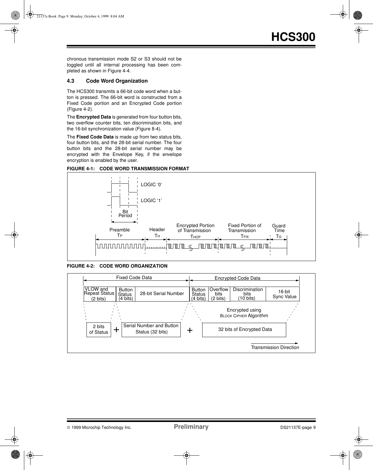
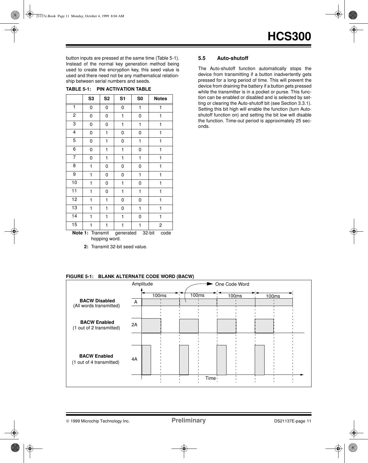
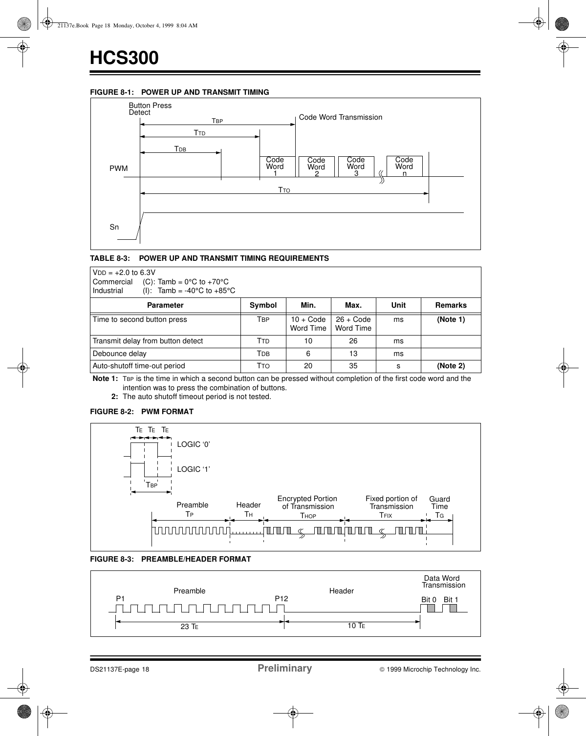
![HCS300DS21137E-page 10 Preliminary 1999 Microchip Technology Inc.FIGURE 4-3: SYNCHRONOUS TRANSMISSION MODEFIGURE 4-4: TRANSMISSION WORD FORMAT DURING SYNCHRONOUS TRANSMISSION MODE5.0 SPECIAL FEATURES5.1 Code Word Completion Code word completion is an automatic feature thatmakes sure that the entire code word is transmitted,even if the button is released before the transmission iscomplete. The HCS300 encoder powers itself up whena button is pushed and powers itself down after thecommand is finished, if the user has already releasedthe button. If the button is held down beyond the timefor one transmission, then multiple transmissions willresult. If another button is activated during atransmission, the active transmission will be abortedand the new code will be generated using the newbutton information. 5.2 Blank Alternate Code Word Federal Communications Commission (FCC) Part 15rules specify the limits on fundamental power andharmonics that can be transmitted. Power is calculatedon the worst case average power transmitted in a100ms window. It is therefore advantageous tominimize the duty cycle of the transmitted word. Thiscan be achieved by minimizing the duty cycle of theindividual bits and by blanking out consecutive words.Blank Alternate Code Word (BACW) is used forreducing the average power of a transmission(Figure 5-1). This is a selectable feature that isdetermined in conjunction with the baudrate selectionbits BSL0 and BSL1. Using the BACW allows the userto transmit a higher amplitude transmission if thetransmission length is shorter. The FCC putsconstraints on the average power that can betransmitted by a device, and BACW effectively preventscontinuous transmission by only allowing the transmis-sion of every second or every fourth code word. Thisreduces the average power transmitted and hence,assists in FCC approval of a transmitter device.5.3 Envelope Encryption OptionEnvelope Encryption is a user selectable option whichis meant to offer a higher level of security for a codehopping system. During a normal transmission with theenvelope encryption turned off, the 28-bit serialnumber is transmitted in the clear (unencrypted). Ifenvelope encryption is selected, then the serial numberis also encrypted before transmission. The encryptionfor the serial number is done using a different algorithmthan the transmission algorithm. The envelopeencryption scheme is not nearly as complex as thealgorithm and, hence, not as secure. When the enve-lope encryption is used, the serial number must bedecrypted using the envelope key and envelopedecryption. After the serial number is obtained, the nor-mal decryption method can be used to decrypt the hop-ping code. All transmitters in a system must use thesame envelope key.5.4 Secure LearnIn order to increase the level of security in a system, itis possible for the receiver to implement what is knownas a secure learn function. This can be done by utilizingthe seed value on the HCS300 which is stored inEEPROM and can only be transmitted when all fourt = 50 ms“01,10,11”PWMS2(S3)S[1:0]16 2 4 28 16 16Transmission DirectionReserved Padding ButtonCode Serial Number Data Word Sync Counter21137e.Book Page 10 Monday, October 4, 1999 8:04 AM](https://usermanual.wiki/Leidos/418M1.manual-hcs300/User-Guide-256525-Page-10.png)