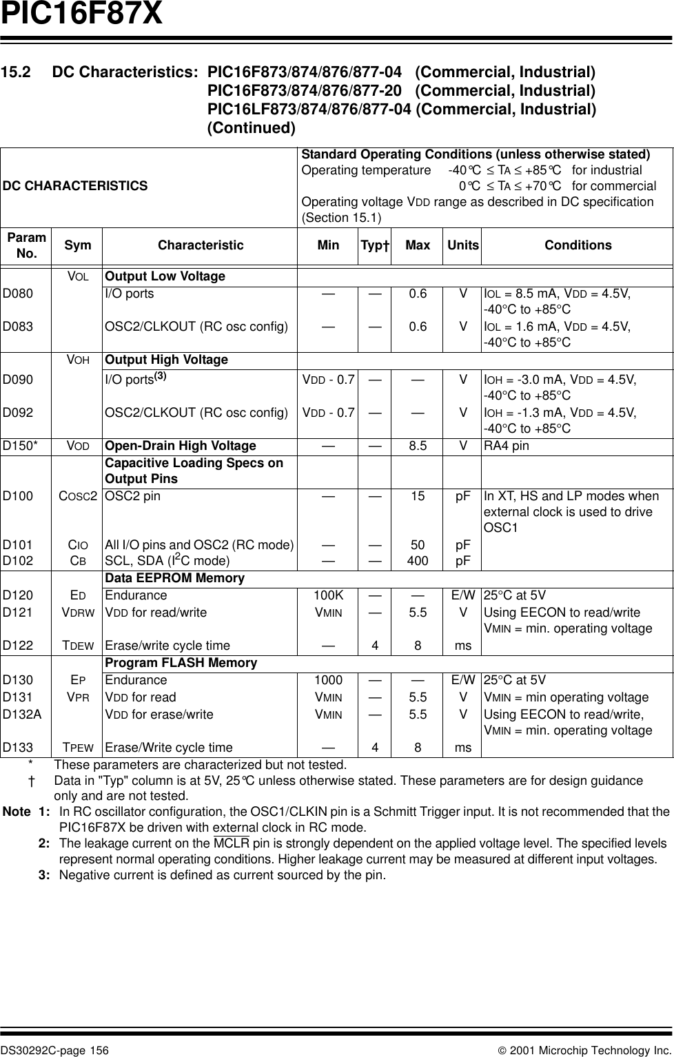
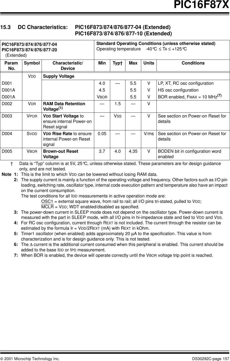
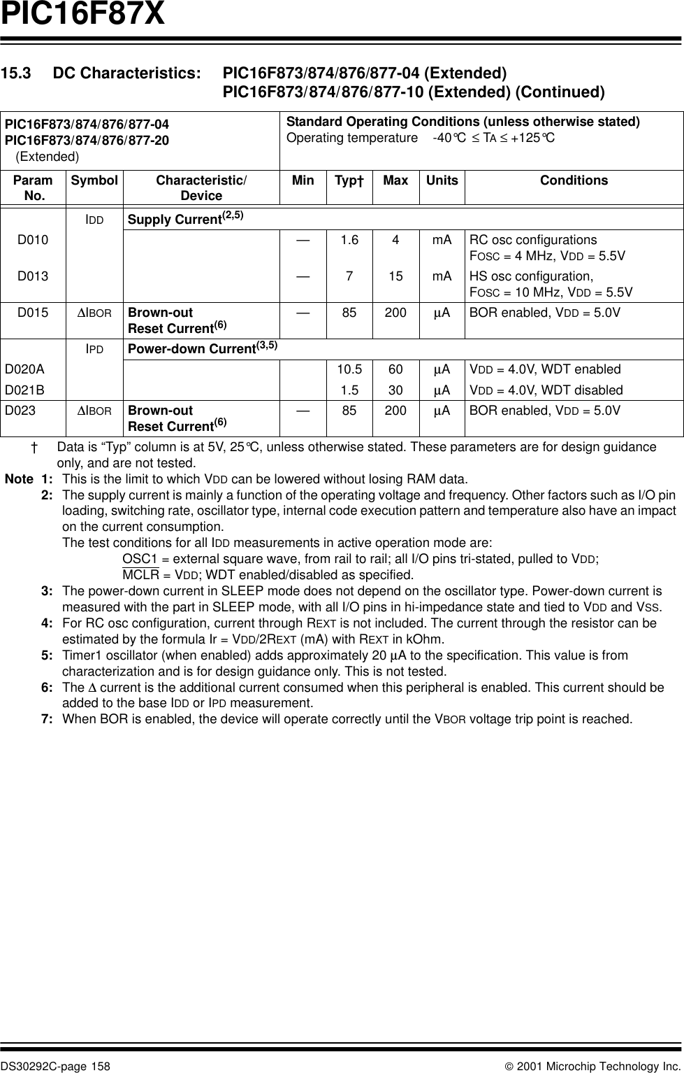
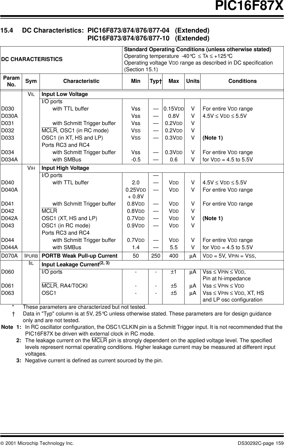
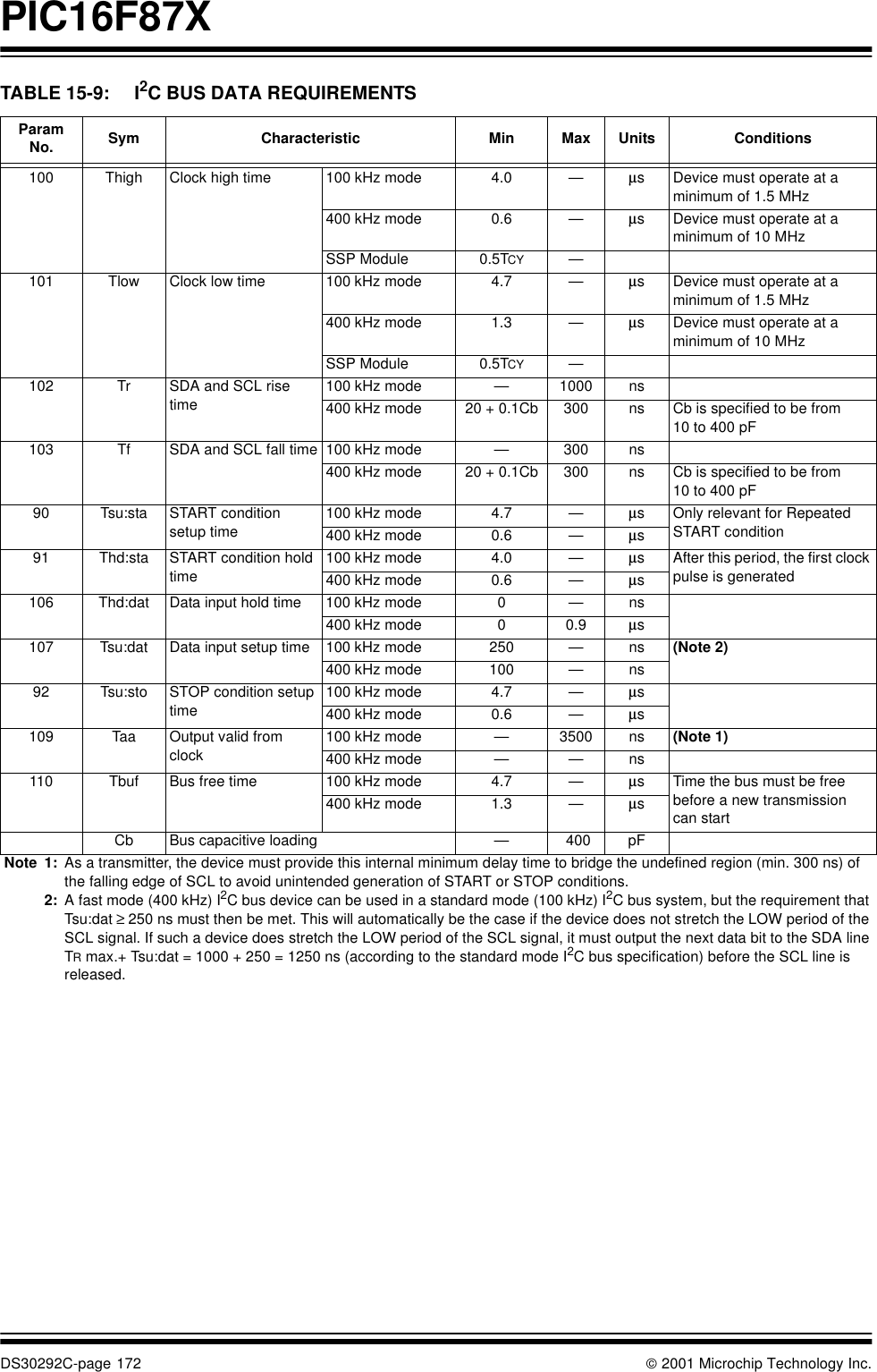
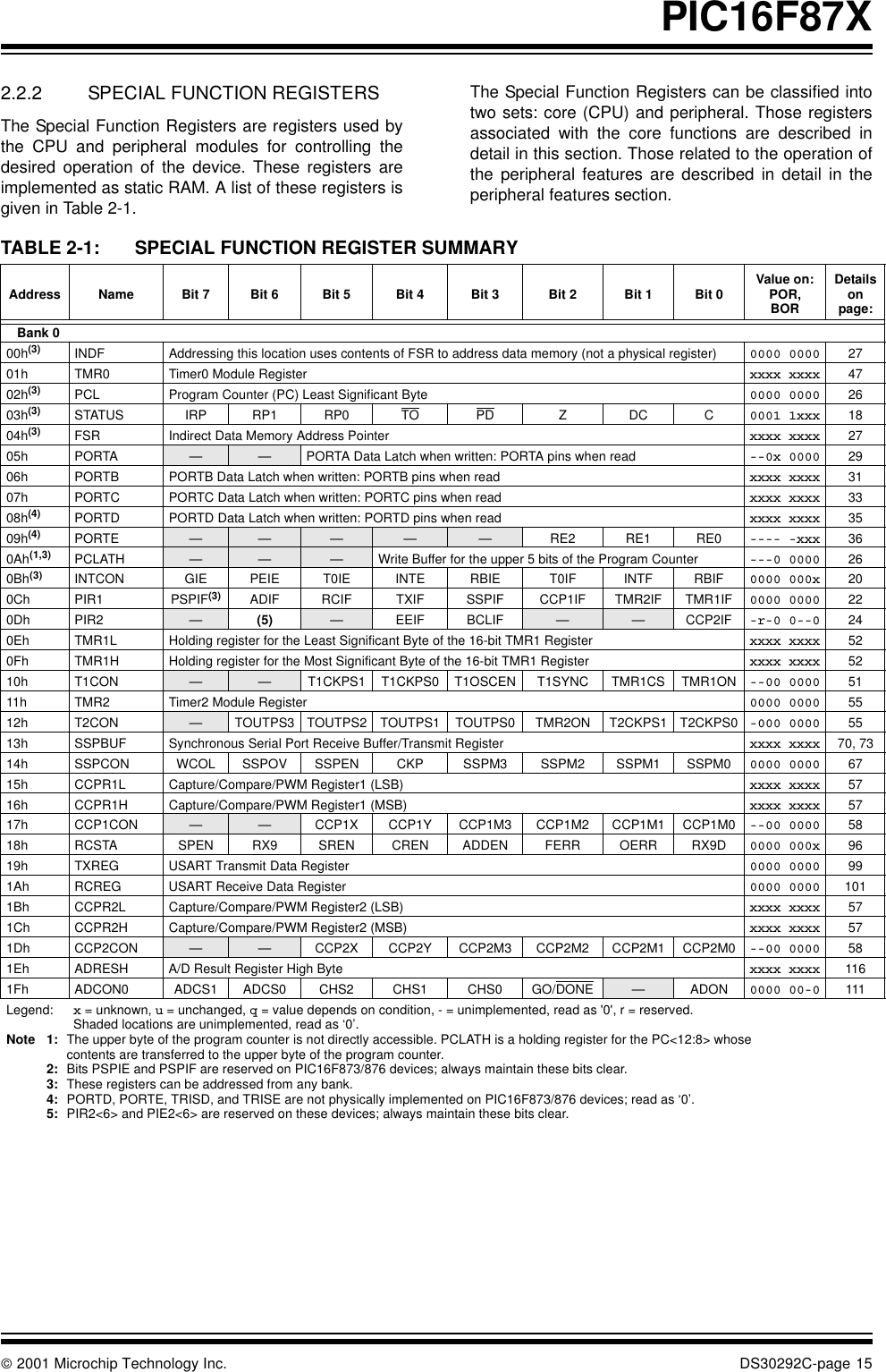
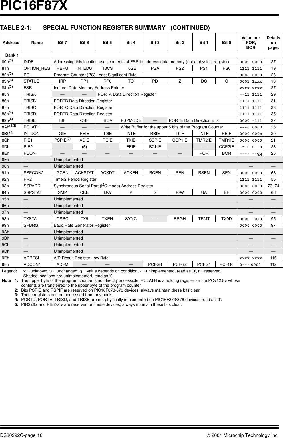
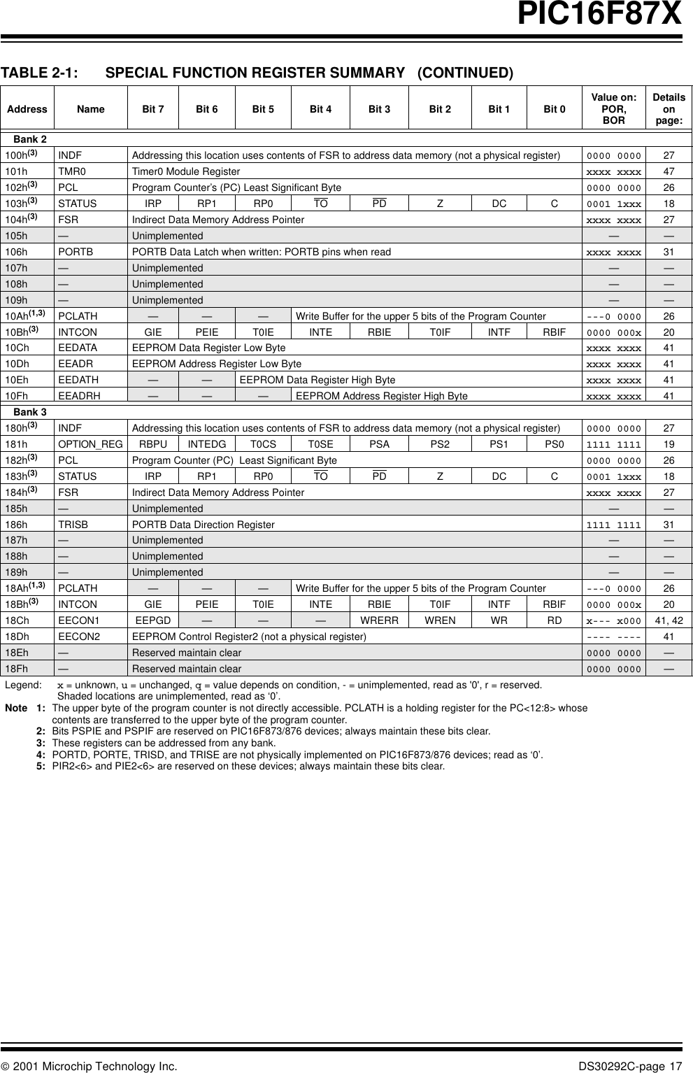
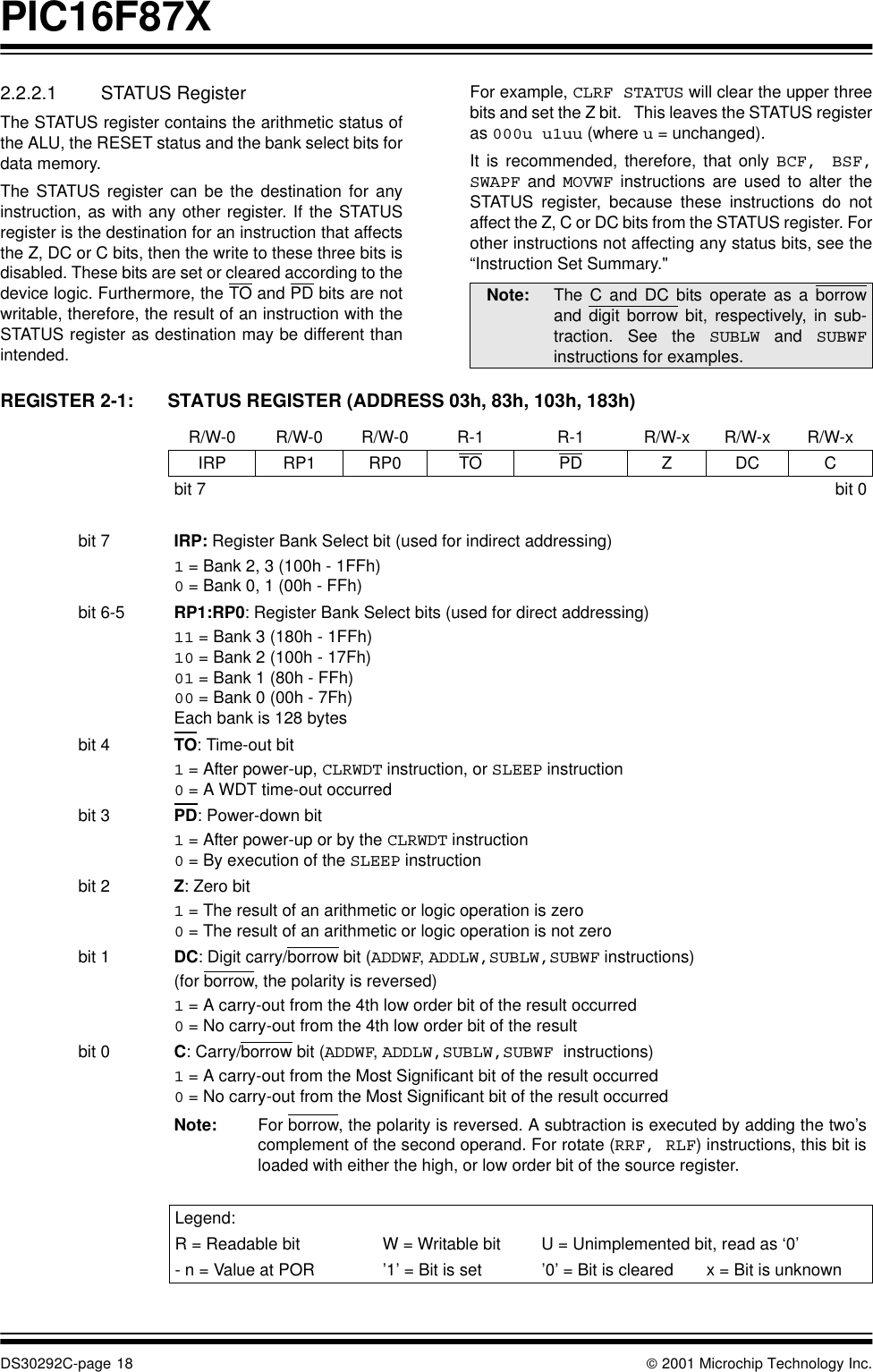
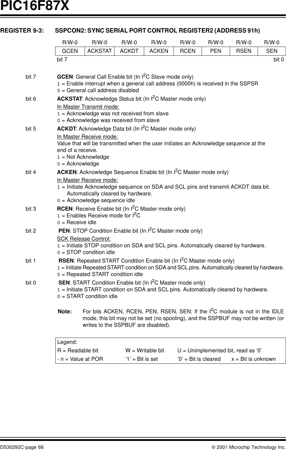
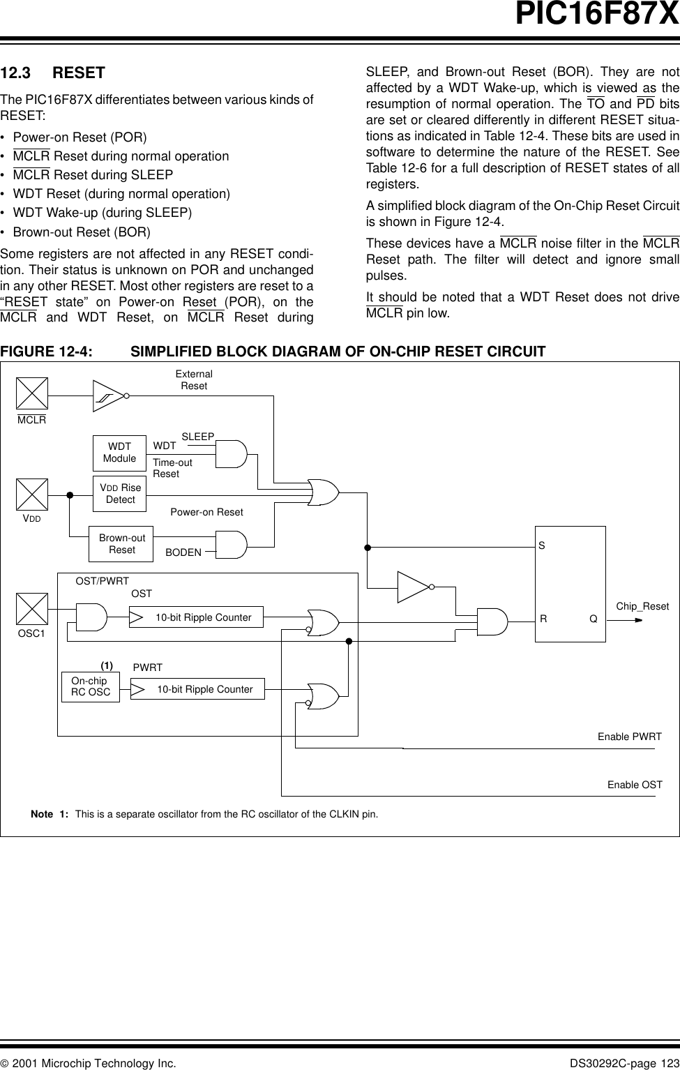
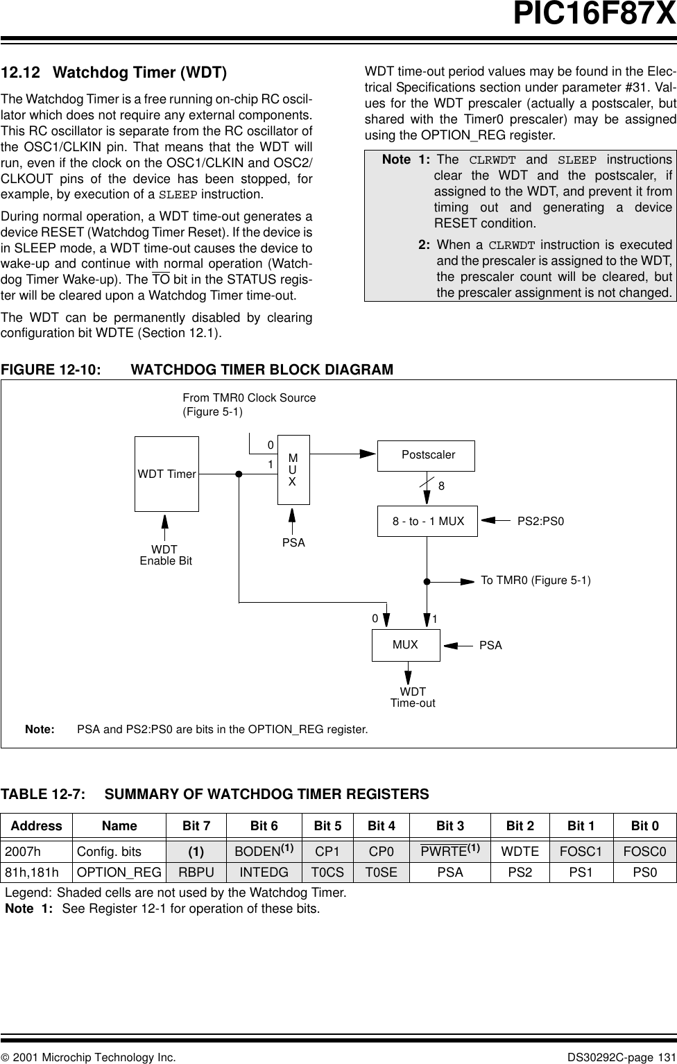
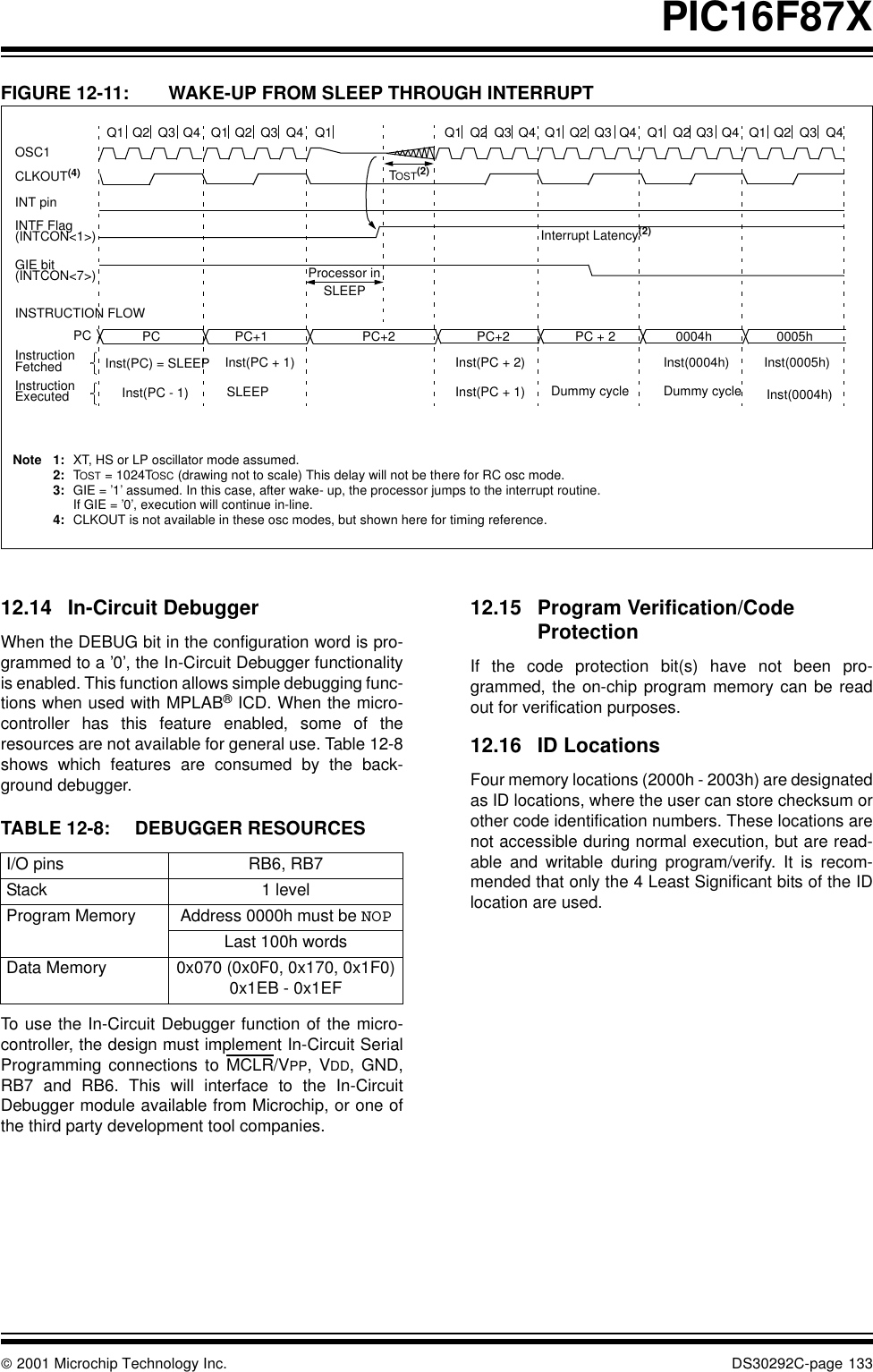
Leidos 418M1 RTR-4 Wireless Option User Manual PIC16F87X Data Sheet
Science Application International Corporation RTR-4 Wireless Option PIC16F87X Data Sheet
Leidos >
Contents
- 1. manual hcs300
- 2. manual pic 16f877
- 3. 1 through 10
- 4. 11 through 17
- 5. 18 throug 21
- 6. 23 through 32
manual pic 16f877
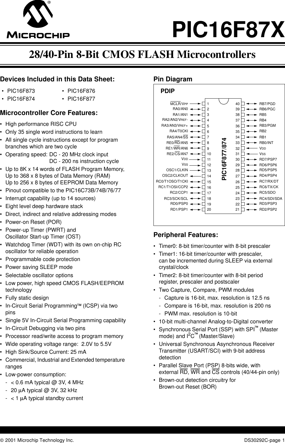


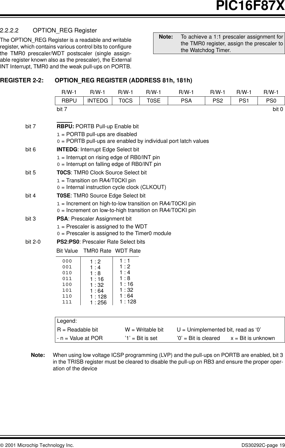
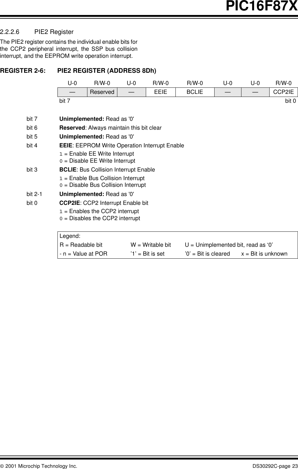


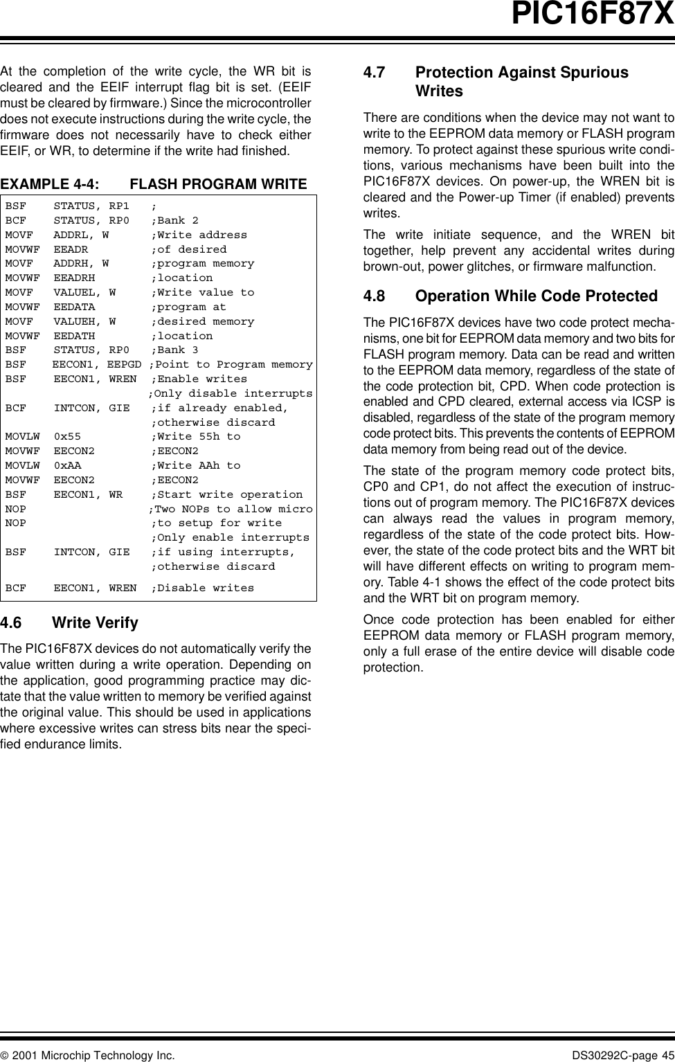

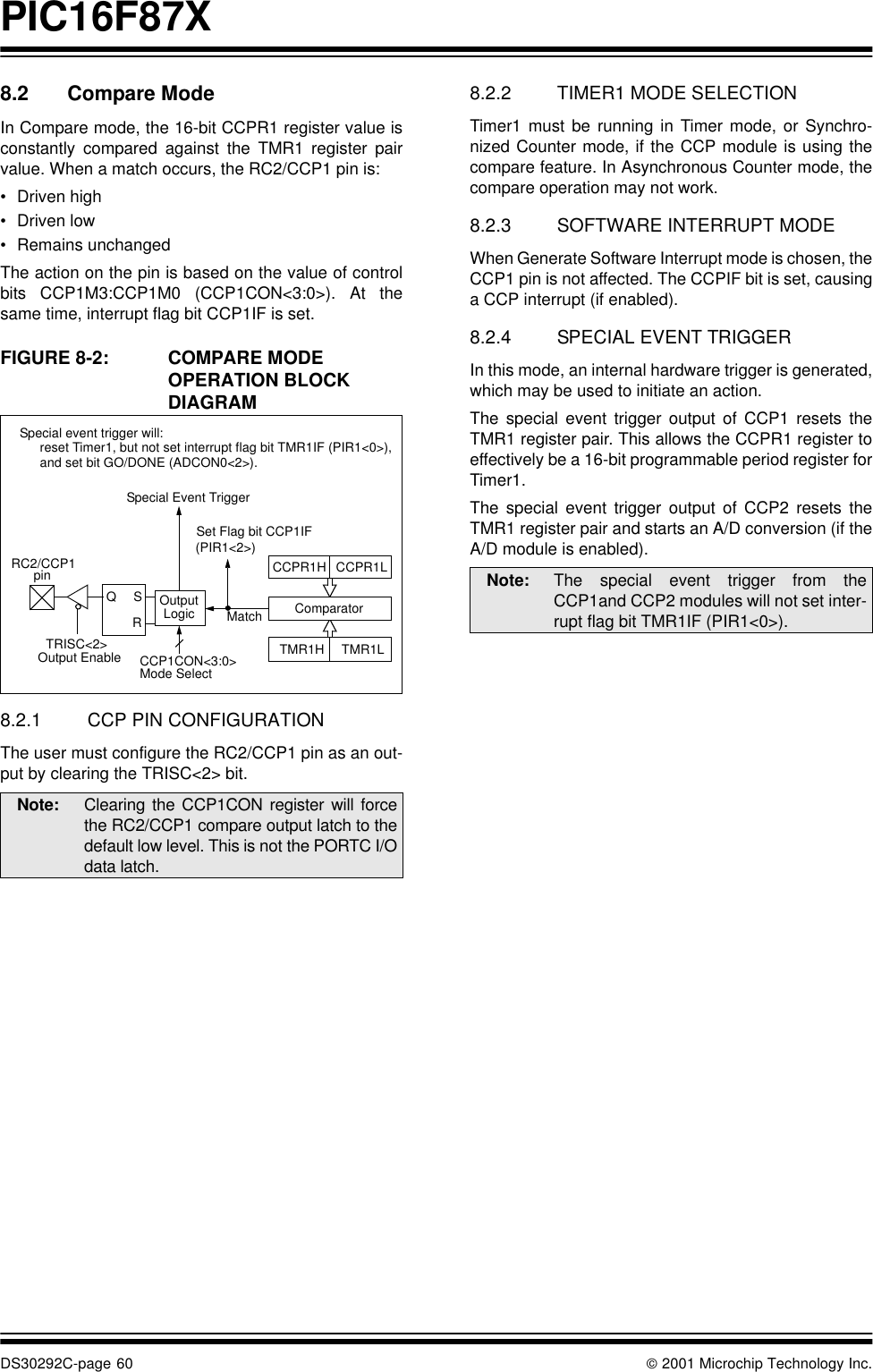
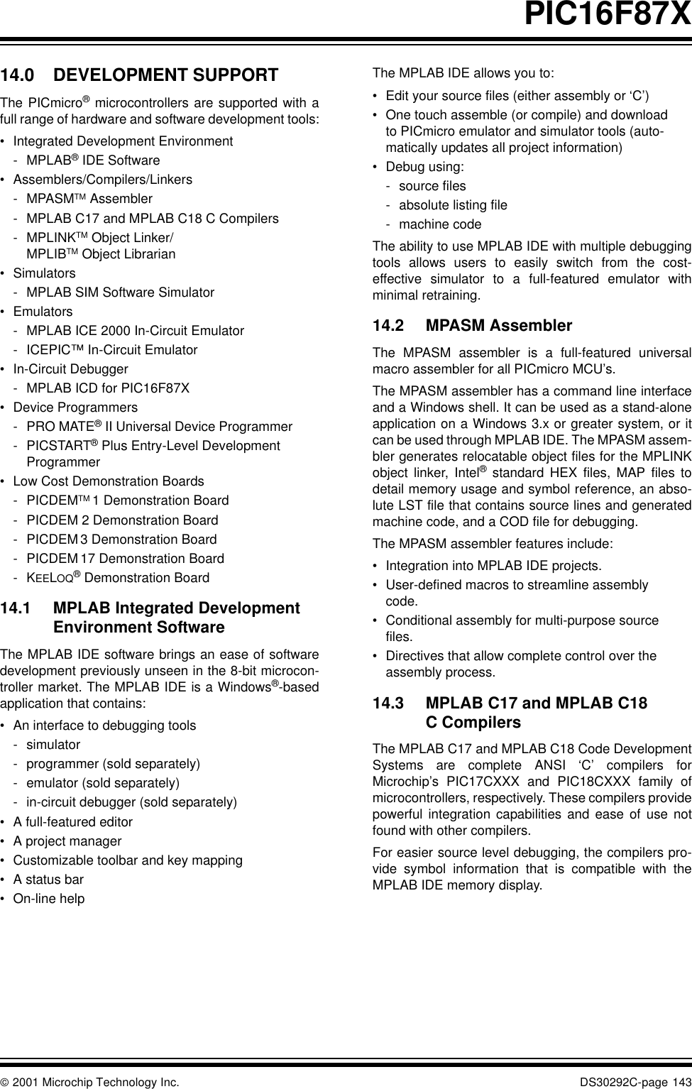
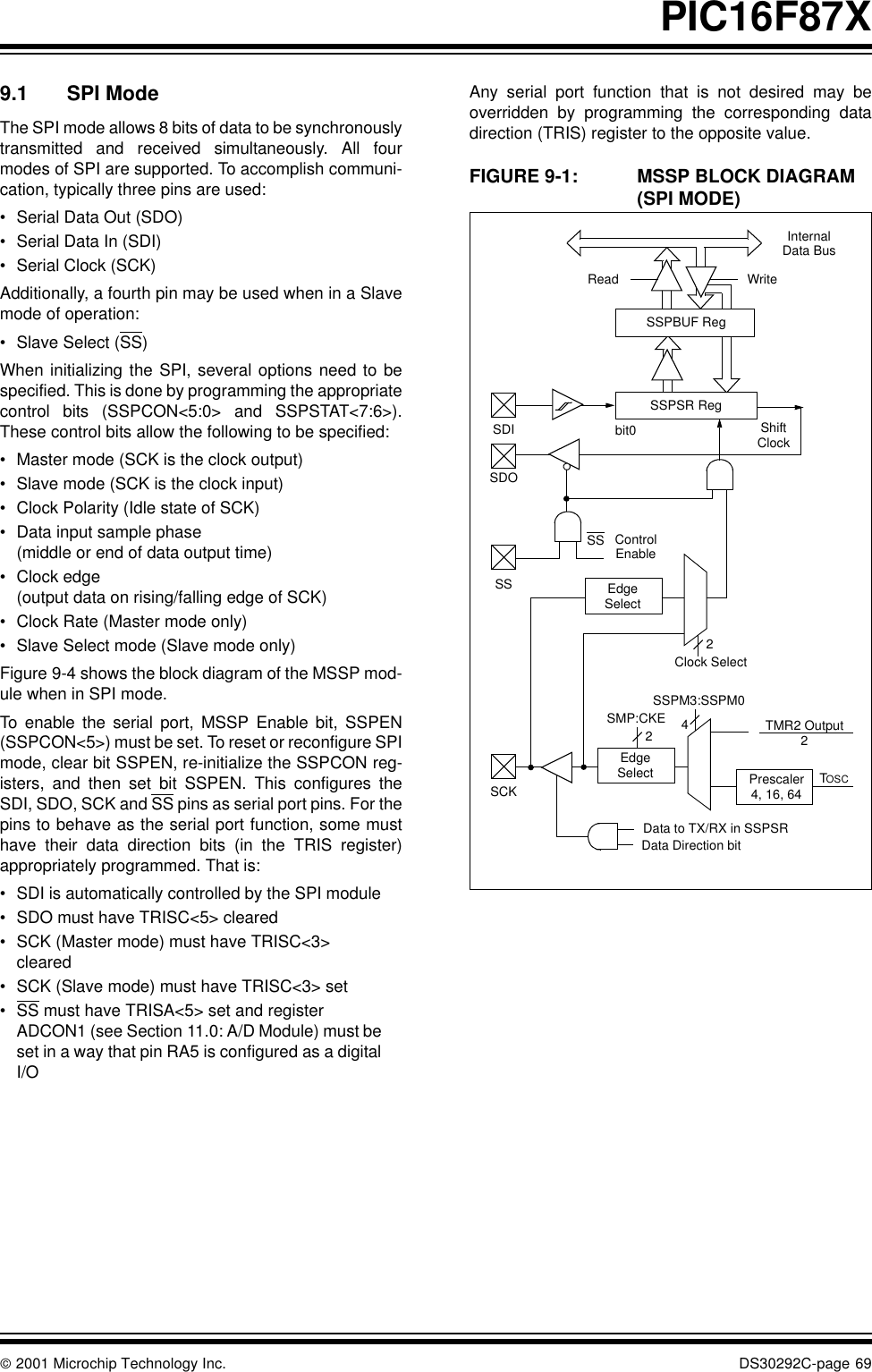
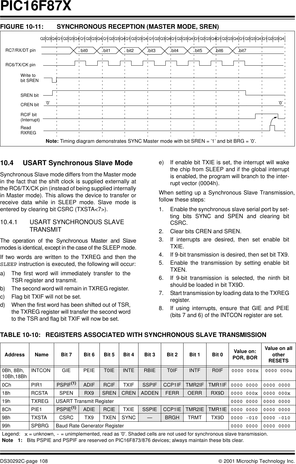
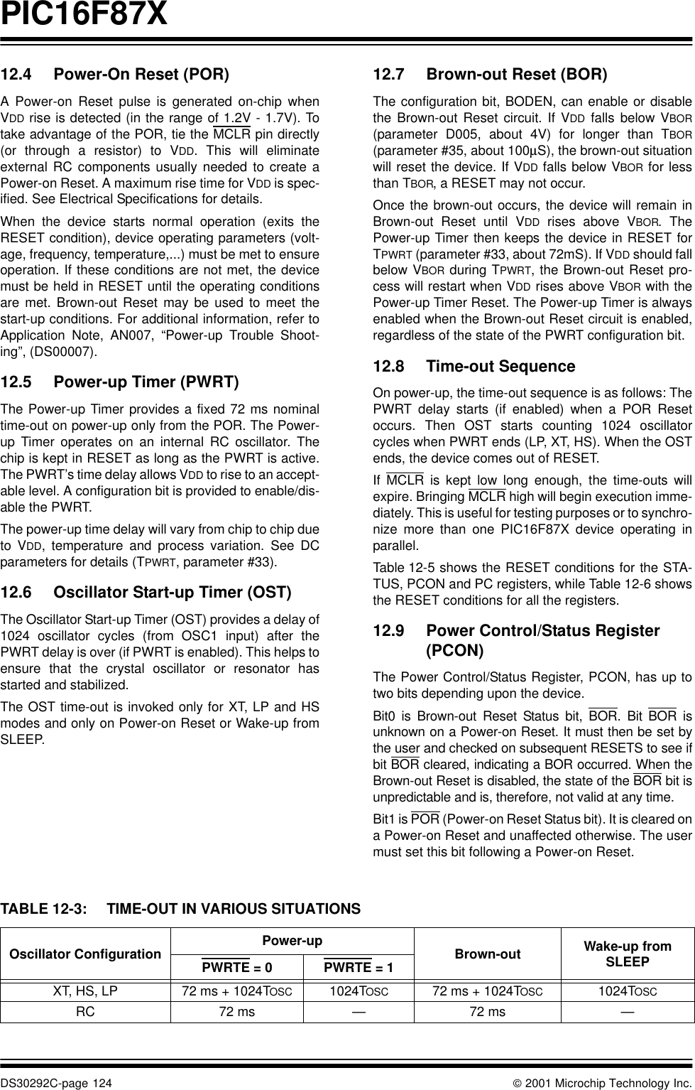
![ 2001 Microchip Technology Inc. DS30292C-page 61PIC16F87X8.3 PWM Mode (PWM)In Pulse Width Modulation mode, the CCPx pin pro-duces up to a 10-bit resolution PWM output. Since theCCP1 pin is multiplexed with the PORTC data latch,the TRISC<2> bit must be cleared to make the CCP1pin an output.Figure 8-3 shows a simplified block diagram of theCCP module in PWM mode.For a step-by-step procedure on how to set up the CCPmodule for PWM operation, see Section 8.3.3.FIGURE 8-3: SIMPLIFIED PWM BLOCK DIAGRAMA PWM output (Figure 8-4) has a time-base (period)and a time that the output stays high (duty cycle). Thefrequency of the PWM is the inverse of the period(1/period).FIGURE 8-4: PWM OUTPUT8.3.1 PWM PERIODThe PWM period is specified by writing to the PR2 reg-ister. The PWM period can be calculated using the fol-lowing formula: PWM period = [(PR2) + 1] • 4 • TOSC •(TMR2 prescale value)PWM frequency is defined as 1 / [PWM period].When TMR2 is equal to PR2, the following three eventsoccur on the next increment cycle:•TMR2 is cleared•The CCP1 pin is set (exception: if PWM duty cycle = 0%, the CCP1 pin will not be set)•The PWM duty cycle is latched from CCPR1L into CCPR1H8.3.2 PWM DUTY CYCLEThe PWM duty cycle is specified by writing to theCCPR1L register and to the CCP1CON<5:4> bits. Upto 10-bit resolution is available. The CCPR1L containsthe eight MSbs and the CCP1CON<5:4> contains thetwo LSbs. This 10-bit value is represented byCCPR1L:CCP1CON<5:4>. The following equation isused to calculate the PWM duty cycle in time: PWM duty cycle =(CCPR1L:CCP1CON<5:4>) • TOSC • (TMR2 prescale value)CCPR1L and CCP1CON<5:4> can be written to at anytime, but the duty cycle value is not latched intoCCPR1H until after a match between PR2 and TMR2occurs (i.e., the period is complete). In PWM mode,CCPR1H is a read-only register.The CCPR1H register and a 2-bit internal latch areused to double buffer the PWM duty cycle. This doublebuffering is essential for glitch-free PWM operation.When the CCPR1H and 2-bit latch match TMR2, con-catenated with an internal 2-bit Q clock, or 2 bits of theTMR2 prescaler, the CCP1 pin is cleared.The maximum PWM resolution (bits) for a given PWMfrequency is given by the formula:Note: Clearing the CCP1CON register will forcethe CCP1 PWM output latch to the defaultlow level. This is not the PORTC I/O datalatch.CCPR1LCCPR1H (Slave)ComparatorTMR2ComparatorPR2(Note 1)RQSDuty Cycle Registers CCP1CON<5:4>Clear Timer,CCP1 pin and latch D.C.TRISC<2>RC2/CCP1Note 1: The 8-bit timer is concatenated with 2-bit internal Qclock, or 2 bits of the prescaler, to create 10-bit time-base.PeriodDuty CycleTMR2 = PR2TMR2 = Duty CycleTMR2 = PR2Note: The Timer2 postscaler (see Section 7.1) isnot used in the determination of the PWMfrequency. The postscaler could be usedto have a servo update rate at a differentfrequency than the PWM output.Note: If the PWM duty cycle value is longer thanthe PWM period, the CCP1 pin will not becleared.log(FPWMlog(2)FOSC )bits=Resolution](https://usermanual.wiki/Leidos/418M1.manual-pic-16f877/User-Guide-256526-Page-63.png)

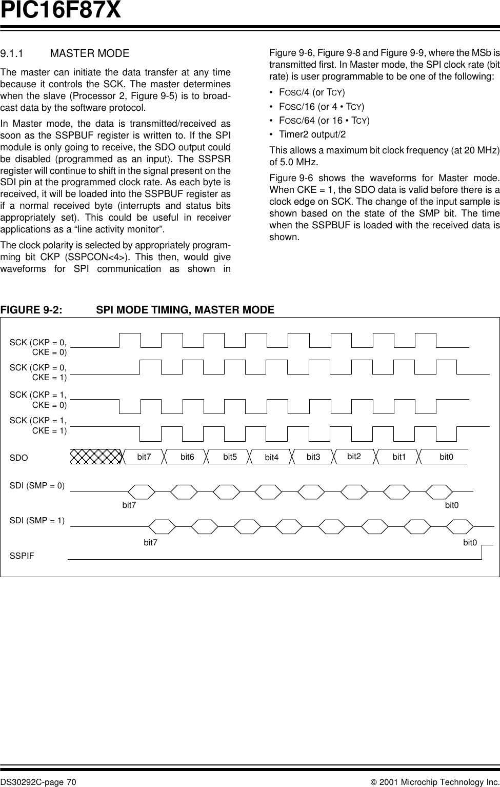
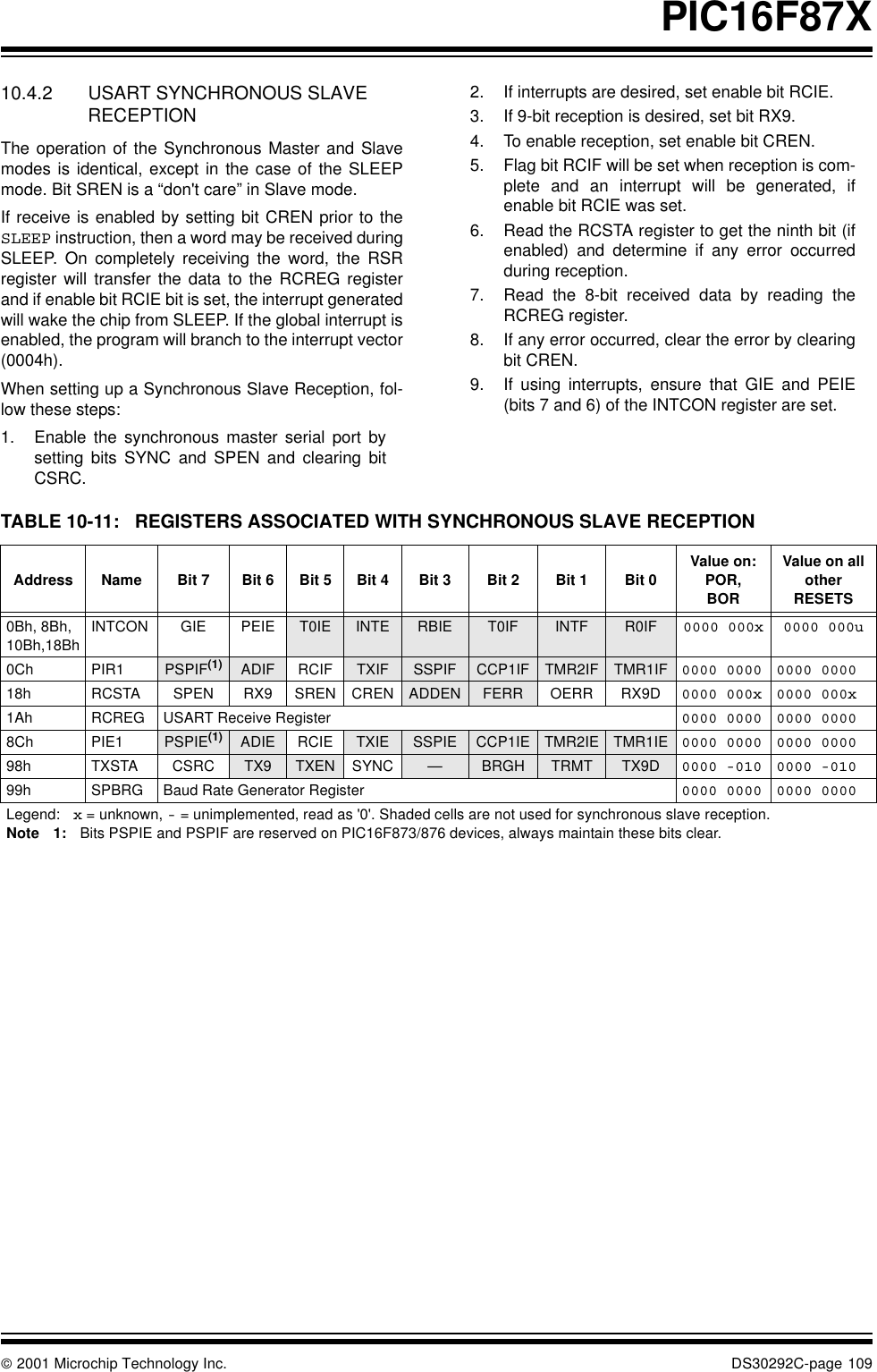

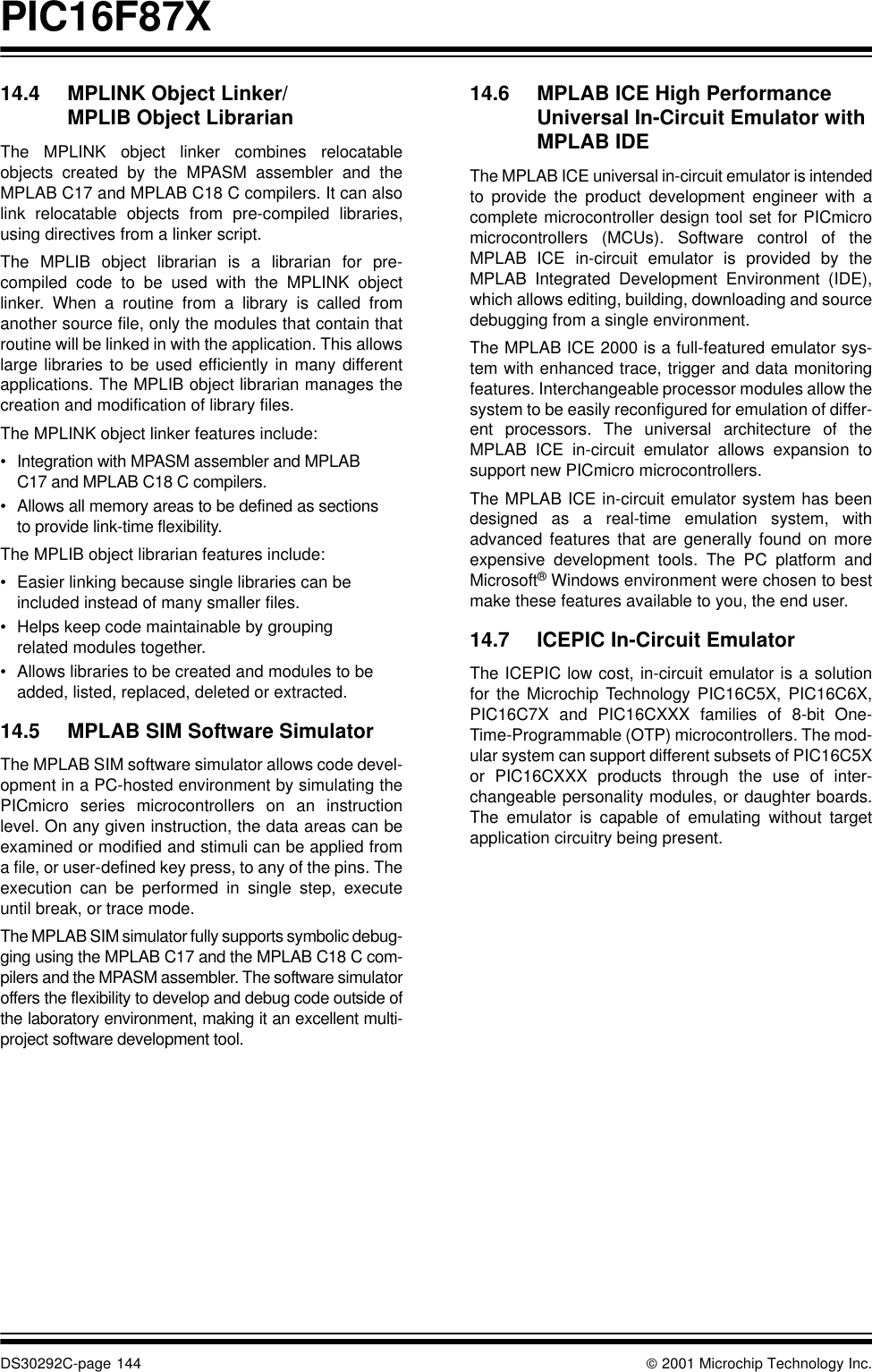
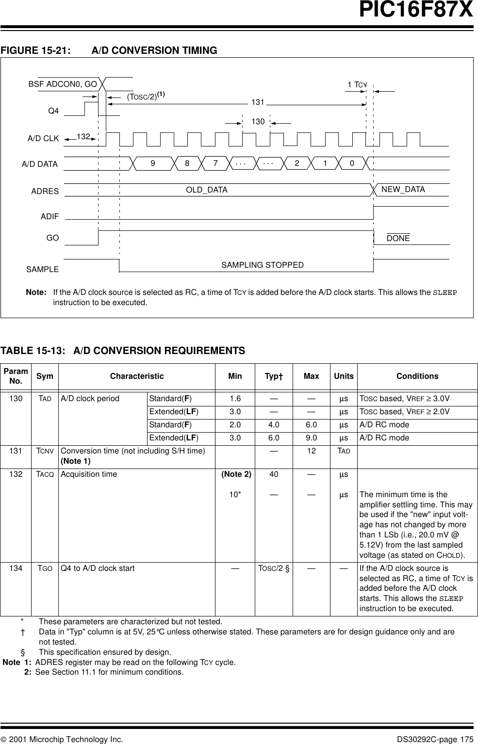
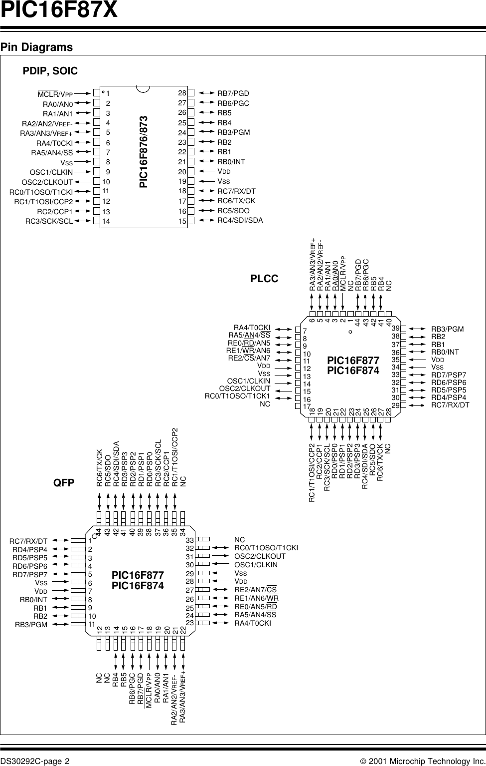
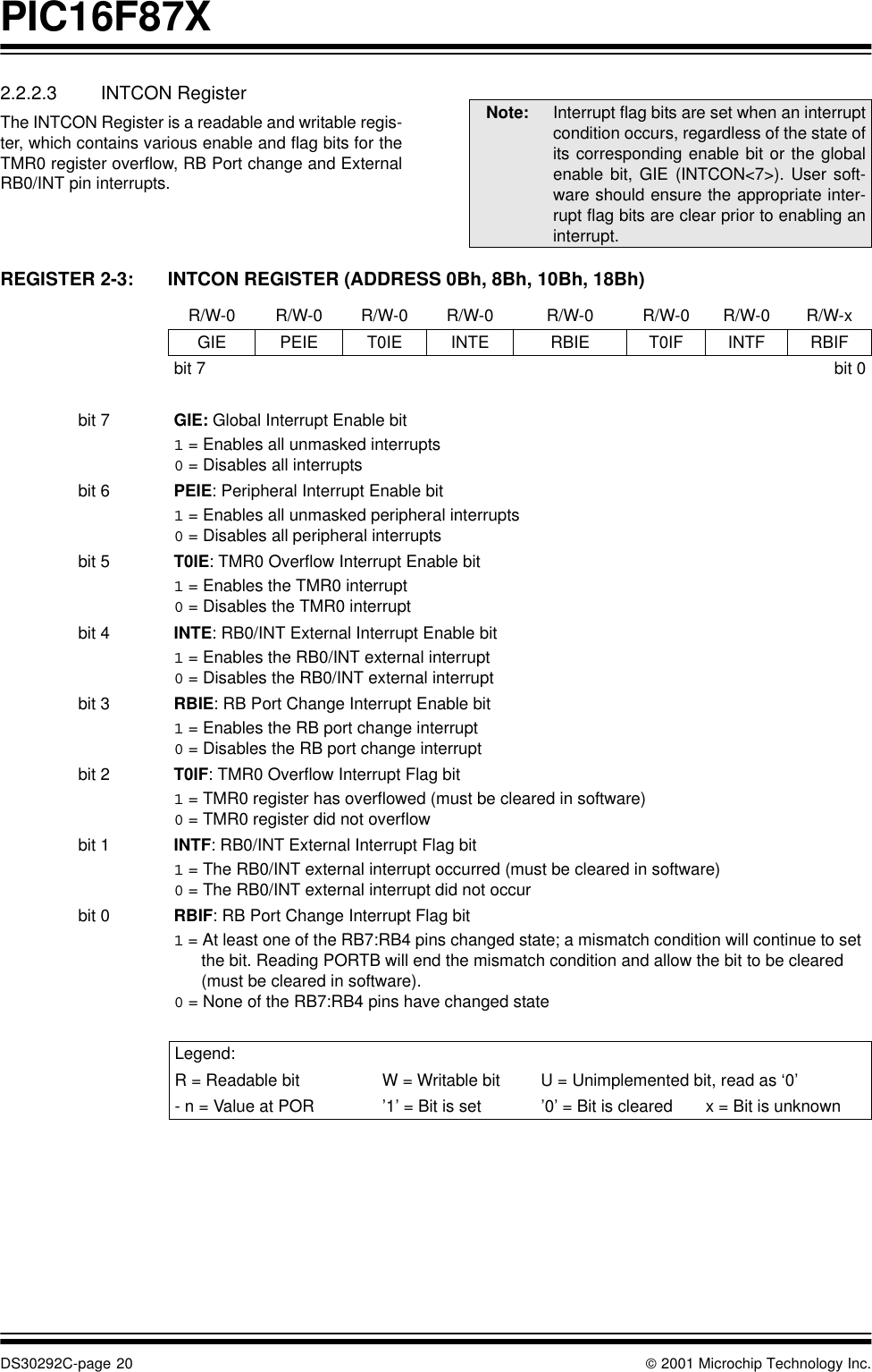
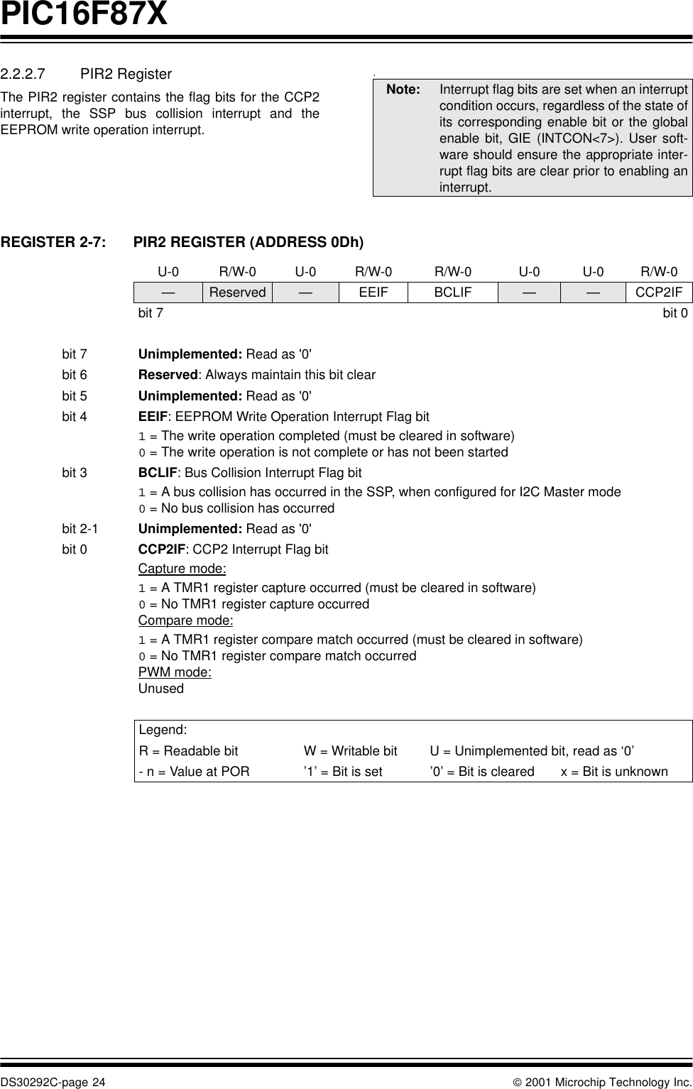
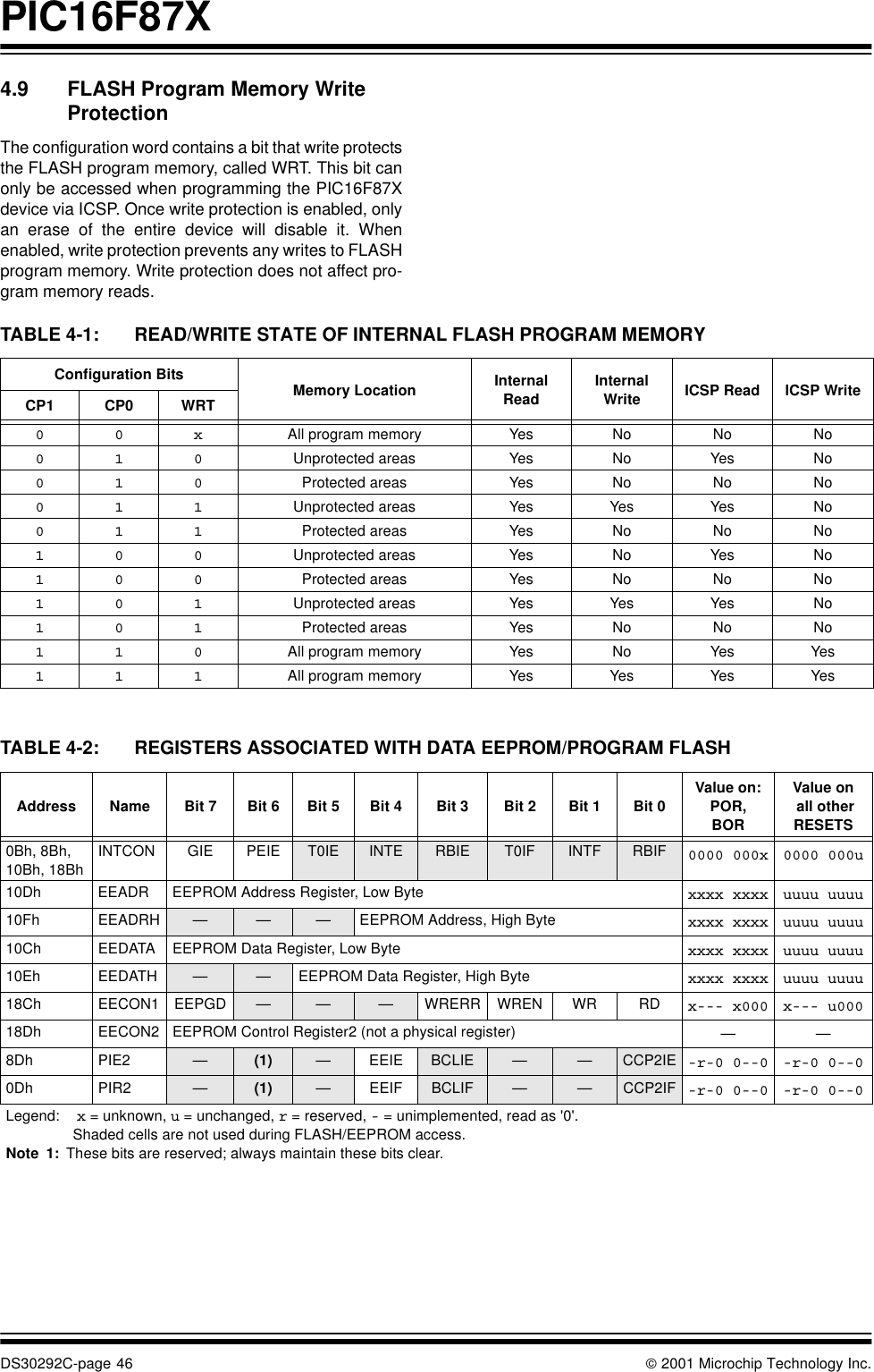
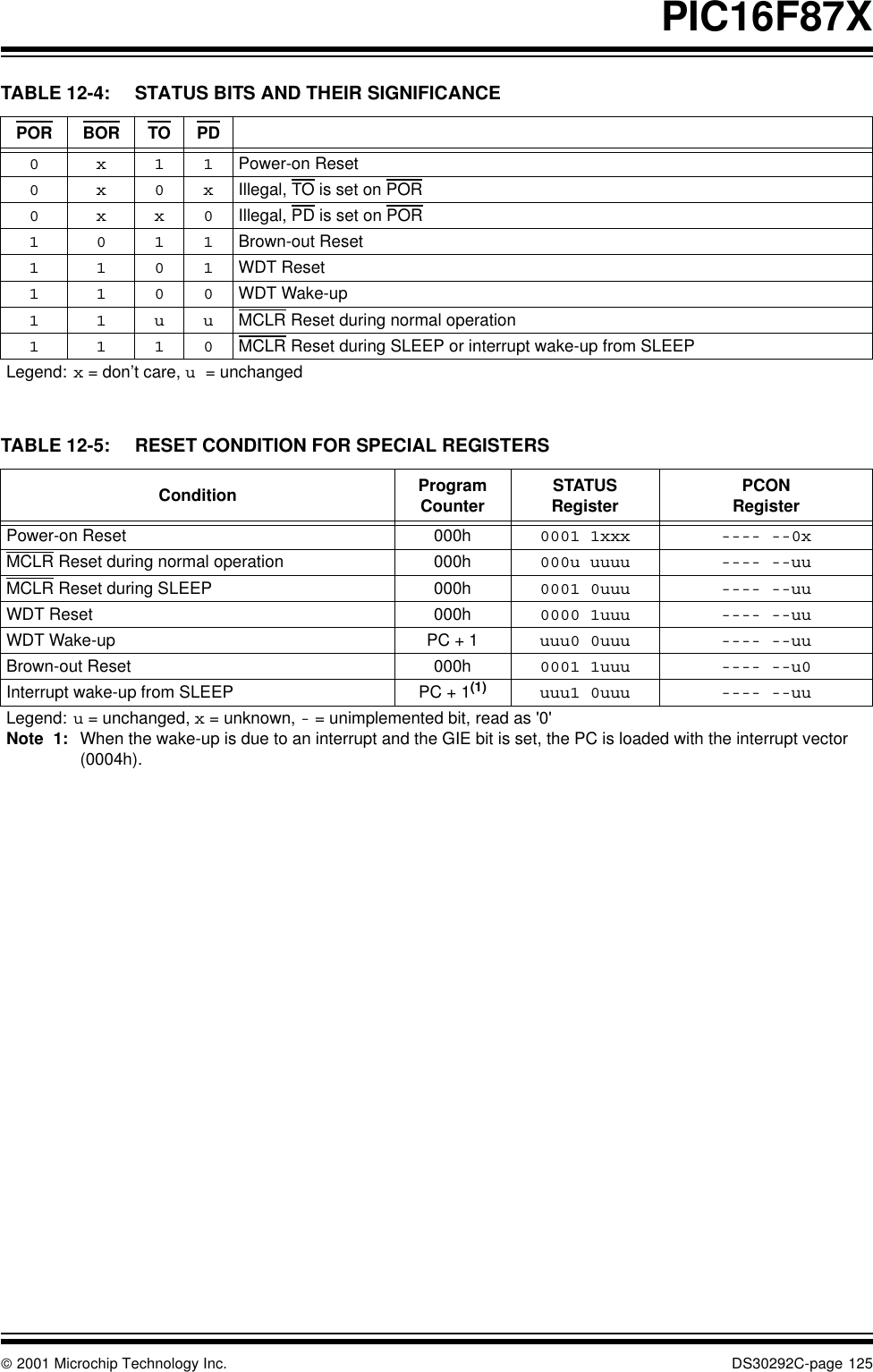
![PIC16F87XDS30292C-page 114 2001 Microchip Technology Inc.11.1 A/D Acquisition Requirements For the A/D converter to meet its specified accuracy,the charge holding capacitor (CHOLD) must be allowedto fully charge to the input channel voltage level. Theanalog input model is shown in Figure 11-2. The sourceimpedance (RS) and the internal sampling switch (RSS)impedance directly affect the time required to chargethe capacitor CHOLD. The sampling switch (RSS)impedance varies over the device voltage (VDD), seeFigure 11-2. The maximum recommended imped-ance for analog sources is 10 kΩ. As the impedanceis decreased, the acquisition time may be decreased.After the analog input channel is selected (changed),this acquisition must be done before the conversioncan be started.To calculate the minimum acquisition time,Equation 11-1 may be used. This equation assumesthat 1/2 LSb error is used (1024 steps for the A/D). The1/2 LSb error is the maximum error allowed for the A/Dto meet its specified resolution.To calculate the minimum acquisition time, TACQ, seethe PICmicro™ Mid-Range Reference Manual(DS33023).EQUATION 11-1: ACQUISITION TIME FIGURE 11-2: ANALOG INPUT MODEL TACQTCTACQ========Amplifier Settling Time +Hold Capacitor Charging Time +Temperature CoefficientTAMP + TC + TCOFF2µs + TC + [(Temperature -25°C)(0.05µs/°C)] CHOLD (RIC + RSS + RS) In(1/2047)- 120pF (1kΩ + 7kΩ + 10kΩ) In(0.0004885)16.47µs2µs + 16.47µs + [(50°C -25°C)(0.05µs/°C)19.72µsNote 1: The reference voltage (VREF) has no effect on the equation, since it cancels itself out.2: The charge holding capacitor (CHOLD) is not discharged after each conversion.3: The maximum recommended impedance for analog sources is 10 kΩ. This is required to meet the pin leak-age specification.4: After a conversion has completed, a 2.0TAD delay must complete before acquisition can begin again. During this time, the holding capacitor is not connected to the selected A/D input channel.CPINVARSANx5 pFVDDVT = 0.6VVT = 0.6V I LEAKAGERIC ≤ 1kSamplingSwitchSS RSSCHOLD= DAC capacitanceVSS6VSampling Switch5V4V3V2V567891011(kΩ)VDD= 120 pF± 500 nALegend CPINVTI LEAKAGERICSSCHOLD= input capacitance= threshold voltage= leakage current at the pin due to= interconnect resistance= sampling switch= sample/hold capacitance (from DAC)various junctions](https://usermanual.wiki/Leidos/418M1.manual-pic-16f877/User-Guide-256526-Page-116.png)

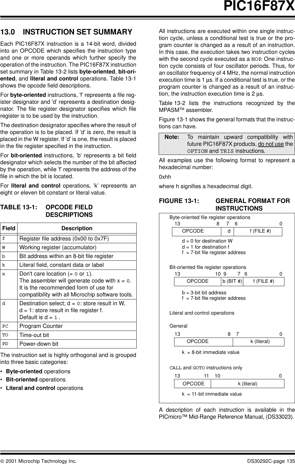
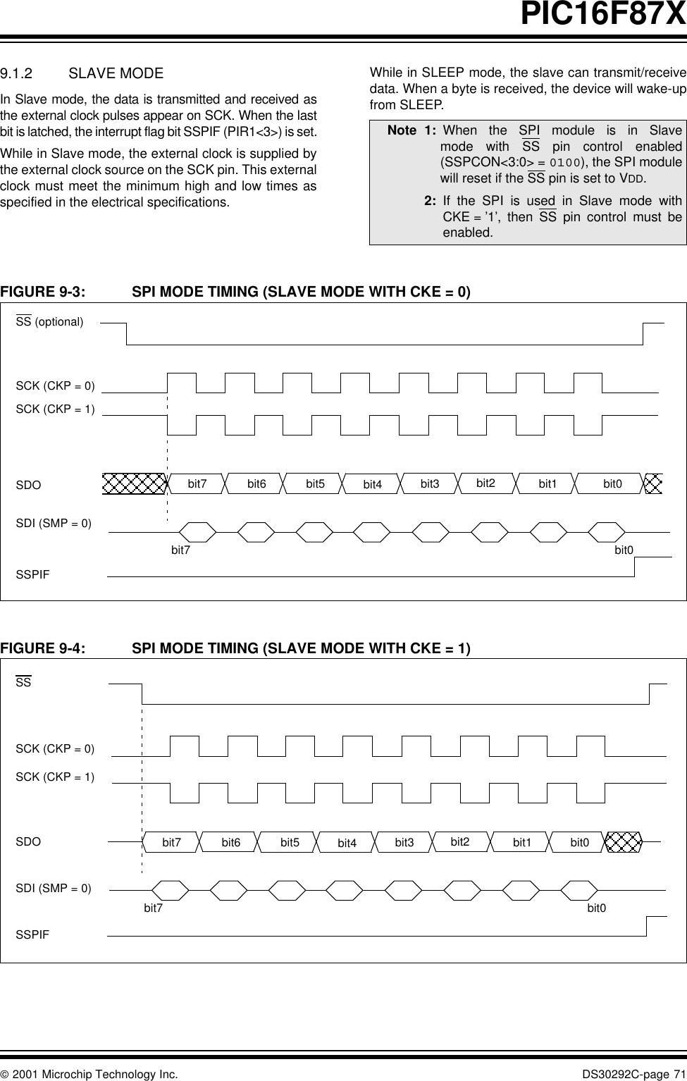
![ 2001 Microchip Technology Inc. DS30292C-page 137PIC16F87X13.1 Instruction Descriptions ADDLW Add Literal and WSyntax: [label] ADDLW kOperands: 0 ≤ k ≤ 255Operation: (W) + k → (W)Status Affected: C, DC, ZDescription: The contents of the W register are added to the eight bit literal ’k’ and the result is placed in the W register.ADDWF Add W and fSyntax: [label] ADDWF f,dOperands: 0 ≤ f ≤ 127d ∈ [0,1]Operation: (W) + (f) → (destination)Status Affected: C, DC, ZDescription: Add the contents of the W register with register ’f’. If ’d’ is 0, the result is stored in the W register. If ’d’ is 1, the result is stored back in register ’f’.ANDLW AND Literal with WSyntax: [label] ANDLW kOperands: 0 ≤ k ≤ 255Operation: (W) .AND. (k) → (W)Status Affected: ZDescription: The contents of W register are AND’ed with the eight bit literal 'k'. The result is placed in the W register.ANDWF AND W with fSyntax: [label] ANDWF f,dOperands: 0 ≤ f ≤ 127d ∈ [0,1]Operation: (W) .AND. (f) → (destination)Status Affected: ZDescription: AND the W register with register 'f'. If 'd' is 0, the result is stored in the W register. If 'd' is 1, the result is stored back in register 'f'.BCF Bit Clear fSyntax: [label] BCF f,bOperands: 0 ≤ f ≤ 1270 ≤ b ≤ 7Operation: 0 → (f<b>)Status Affected: NoneDescription: Bit 'b' in register 'f' is cleared.BSF Bit Set fSyntax: [label] BSF f,bOperands: 0 ≤ f ≤ 1270 ≤ b ≤ 7Operation: 1 → (f<b>)Status Affected: NoneDescription: Bit 'b' in register 'f' is set.BTFSS Bit Test f, Skip if SetSyntax: [label] BTFSS f,bOperands: 0 ≤ f ≤ 1270 ≤ b < 7Operation: skip if (f<b>) = 1Status Affected: NoneDescription: If bit 'b' in register 'f' is '0', the next instruction is executed.If bit 'b' is '1', then the next instruc-tion is discarded and a NOP is executed instead, making this a 2TCY instruction.BTFSC Bit Test, Skip if ClearSyntax: [label] BTFSC f,bOperands: 0 ≤ f ≤ 1270 ≤ b ≤ 7Operation: skip if (f<b>) = 0Status Affected: NoneDescription: If bit 'b' in register 'f' is '1', the next instruction is executed.If bit 'b', in register 'f', is '0', the next instruction is discarded, and a NOP is executed instead, making this a 2TCY instruction.](https://usermanual.wiki/Leidos/418M1.manual-pic-16f877/User-Guide-256526-Page-139.png)
![PIC16F87XDS30292C-page 138 2001 Microchip Technology Inc.CALL Call SubroutineSyntax: [ label ] CALL kOperands: 0 ≤ k ≤ 2047Operation: (PC)+ 1→ TOS,k → PC<10:0>,(PCLATH<4:3>) → PC<12:11>Status Affected: NoneDescription: Call Subroutine. First, return address (PC+1) is pushed onto the stack. The eleven-bit immedi-ate address is loaded into PC bits <10:0>. The upper bits of the PC are loaded from PCLATH. CALL is a two-cycle instruction.CLRF Clear fSyntax: [label] CLRF fOperands: 0 ≤ f ≤ 127Operation: 00h → (f)1 → ZStatus Affected: ZDescription: The contents of register ’f’ are cleared and the Z bit is set.CLRW Clear WSyntax: [ label ] CLRWOperands: NoneOperation: 00h → (W)1 → ZStatus Affected: ZDescription: W register is cleared. Zero bit (Z) is set.CLRWDT Clear Watchdog TimerSyntax: [ label ] CLRWDTOperands: NoneOperation: 00h → WDT0 → WDT prescaler,1 → TO1 → PDStatus Affected: TO, PDDescription: CLRWDT instruction resets the Watchdog Timer. It also resets the prescaler of the WDT. Status bits TO and PD are set.COMF Complement fSyntax: [ label ] COMF f,dOperands: 0 ≤ f ≤ 127d ∈ [0,1]Operation: (f) → (destination)Status Affected: ZDescription: The contents of register ’f’ are complemented. If ’d’ is 0, the result is stored in W. If ’d’ is 1, the result is stored back in register ’f’.DECF Decrement fSyntax: [label] DECF f,dOperands: 0 ≤ f ≤ 127d ∈ [0,1]Operation: (f) - 1 → (destination)Status Affected: ZDescription: Decrement register ’f’. If ’d’ is 0, the result is stored in the W register. If ’d’ is 1, the result is stored back in register ’f’.](https://usermanual.wiki/Leidos/418M1.manual-pic-16f877/User-Guide-256526-Page-140.png)
![ 2001 Microchip Technology Inc. DS30292C-page 139PIC16F87XDECFSZ Decrement f, Skip if 0Syntax: [ label ] DECFSZ f,dOperands: 0 ≤ f ≤ 127d ∈ [0,1]Operation: (f) - 1 → (destination); skip if result = 0Status Affected: NoneDescription: The contents of register ’f’ are decremented. If ’d’ is 0, the result is placed in the W register. If ’d’ is 1, the result is placed back in register ’f’. If the result is 1, the next instruc-tion is executed. If the result is 0, then a NOP is executed instead making it a 2TCY instruction.GOTO Unconditional BranchSyntax: [ label ] GOTO kOperands: 0 ≤ k ≤ 2047Operation: k → PC<10:0>PCLATH<4:3> → PC<12:11>Status Affected: NoneDescription: GOTO is an unconditional branch. The eleven-bit immediate value is loaded into PC bits <10:0>. The upper bits of PC are loaded from PCLATH<4:3>. GOTO is a two-cycle instruction.INCF Increment fSyntax: [ label ] INCF f,dOperands: 0 ≤ f ≤ 127d ∈ [0,1]Operation: (f) + 1 → (destination)Status Affected: ZDescription: The contents of register ’f’ are incremented. If ’d’ is 0, the result is placed in the W register. If ’d’ is 1, the result is placed back in register ’f’.INCFSZ Increment f, Skip if 0Syntax: [ label ] INCFSZ f,dOperands: 0 ≤ f ≤ 127d ∈ [0,1]Operation: (f) + 1 → (destination), skip if result = 0Status Affected: NoneDescription: The contents of register ’f’ are incremented. If ’d’ is 0, the result is placed in the W register. If ’d’ is 1, the result is placed back in register ’f’.If the result is 1, the next instruc-tion is executed. If the result is 0, a NOP is executed instead, making it a 2TCY instruction.IORLW Inclusive OR Literal with WSyntax: [ label ] IORLW kOperands: 0 ≤ k ≤ 255Operation: (W) .OR. k → (W)Status Affected: ZDescription: The contents of the W register are OR’ed with the eight bit literal 'k'. The result is placed in the W register.IORWF Inclusive OR W with fSyntax: [ label ] IORWF f,dOperands: 0 ≤ f ≤ 127d ∈ [0,1]Operation: (W) .OR. (f) → (destination)Status Affected: ZDescription: Inclusive OR the W register with register 'f'. If 'd' is 0 the result is placed in the W register. If 'd' is 1 the result is placed back in register 'f'.](https://usermanual.wiki/Leidos/418M1.manual-pic-16f877/User-Guide-256526-Page-141.png)
![PIC16F87XDS30292C-page 140 2001 Microchip Technology Inc.MOVF Move fSyntax: [ label ] MOVF f,dOperands: 0 ≤ f ≤ 127d ∈ [0,1]Operation: (f) → (destination)Status Affected: ZDescription: The contents of register f are moved to a destination dependant upon the status of d. If d = 0, destination is W register. If d = 1, the destination is file register f itself. d = 1 is useful to test a file register, since status flag Z is affected.MOVLW Move Literal to WSyntax: [ label ] MOVLW kOperands: 0 ≤ k ≤ 255Operation: k → (W)Status Affected: NoneDescription: The eight bit literal ’k’ is loaded into W register. The don’t cares will assemble as 0’s.MOVWF Move W to fSyntax: [ label ] MOVWF fOperands: 0 ≤ f ≤ 127Operation: (W) → (f)Status Affected: NoneDescription: Move data from W register to register 'f'.NOP No OperationSyntax: [ label ] NOPOperands: NoneOperation: No operationStatus Affected: NoneDescription: No operation.RETFIE Return from InterruptSyntax: [ label ] RETFIEOperands: NoneOperation: TOS → PC,1 → GIEStatus Affected: NoneRETLW Return with Literal in WSyntax: [ label ] RETLW kOperands: 0 ≤ k ≤ 255Operation: k → (W); TOS → PCStatus Affected: NoneDescription: The W register is loaded with the eight bit literal 'k'. The program counter is loaded from the top of the stack (the return address). This is a two-cycle instruction.](https://usermanual.wiki/Leidos/418M1.manual-pic-16f877/User-Guide-256526-Page-142.png)
![ 2001 Microchip Technology Inc. DS30292C-page 141PIC16F87XRLF Rotate Left f through CarrySyntax: [ label ] RLF f,dOperands: 0 ≤ f ≤ 127d ∈ [0,1]Operation: See description belowStatus Affected: CDescription: The contents of register ’f’ are rotated one bit to the left through the Carry Flag. If ’d’ is 0, the result is placed in the W register. If ’d’ is 1, the result is stored back in register ’f’.RETURN Return from SubroutineSyntax: [ label ] RETURNOperands: NoneOperation: TOS → PCStatus Affected: NoneDescription: Return from subroutine. The stack is POPed and the top of the stack (TOS) is loaded into the program counter. This is a two-cycle instruction.RRF Rotate Right f through CarrySyntax: [ label ] RRF f,dOperands: 0 ≤ f ≤ 127d ∈ [0,1]Operation: See description belowStatus Affected: CDescription: The contents of register ’f’ are rotated one bit to the right through the Carry Flag. If ’d’ is 0, the result is placed in the W register. If ’d’ is 1, the result is placed back in register ’f’.Register fCRegister fCSLEEPSyntax: [ label ] SLEEPOperands: NoneOperation: 00h → WDT,0 → WDT prescaler,1 → TO,0 → PDStatus Affected: TO, PDDescription: The power-down status bit, PD is cleared. Time-out status bit, TO is set. Watchdog Timer and its prescaler are cleared.The processor is put into SLEEP mode with the oscillator stopped. SUBLW Subtract W from LiteralSyntax: [ label ] SUBLW kOperands: 0 ≤ k ≤ 255Operation: k - (W) → (W)Status Affected: C, DC, ZDescription: The W register is subtracted (2’s complement method) from the eight-bit literal 'k'. The result is placed in the W register.SUBWF Subtract W from fSyntax: [ label ] SUBWF f,dOperands: 0 ≤ f ≤ 127d ∈ [0,1]Operation: (f) - (W) → (destination)Status Affected: C, DC, ZDescription: Subtract (2’s complement method) W register from register 'f'. If 'd' is 0, the result is stored in the W register. If 'd' is 1, the result is stored back in register 'f'.](https://usermanual.wiki/Leidos/418M1.manual-pic-16f877/User-Guide-256526-Page-143.png)
![PIC16F87XDS30292C-page 142 2001 Microchip Technology Inc.SWAPF Swap Nibbles in fSyntax: [ label ] SWAPF f,dOperands: 0 ≤ f ≤ 127d ∈ [0,1]Operation: (f<3:0>) → (destination<7:4>),(f<7:4>) → (destination<3:0>)Status Affected: NoneDescription: The upper and lower nibbles of register ’f’ are exchanged. If ’d’ is 0, the result is placed in the W register. If ’d’ is 1, the result is placed in register ’f’.XORLW Exclusive OR Literal with WSyntax: [label] XORLW kOperands: 0 ≤ k ≤ 255Operation: (W) .XOR. k → (W)Status Affected: ZDescription: The contents of the W register are XOR’ed with the eight-bit lit-eral 'k'. The result is placed in the W register.XORWF Exclusive OR W with fSyntax: [label] XORWF f,dOperands: 0 ≤ f ≤ 127d ∈ [0,1]Operation: (W) .XOR. (f) → (destination)Status Affected: ZDescription: Exclusive OR the contents of the W register with register 'f'. If 'd' is 0, the result is stored in the W register. If 'd' is 1, the result is stored back in register 'f'.](https://usermanual.wiki/Leidos/418M1.manual-pic-16f877/User-Guide-256526-Page-144.png)