NEXCOM VTC6110X00 Intelligent Vehicle Telematics Computer User Manual 2
NEXCOM international Co.,LTD Intelligent Vehicle Telematics Computer 2
NEXCOM >
Contents
- 1. User manual1
- 2. User manual2
- 3. User manual3
- 4. User manual4
- 5. User Manual4
User manual2
Copyright © 2009 NEXCOM International Co., Ltd. All Rights Reserved. 7VTC 6110 User Manual
Chapter 1: Product Introduction
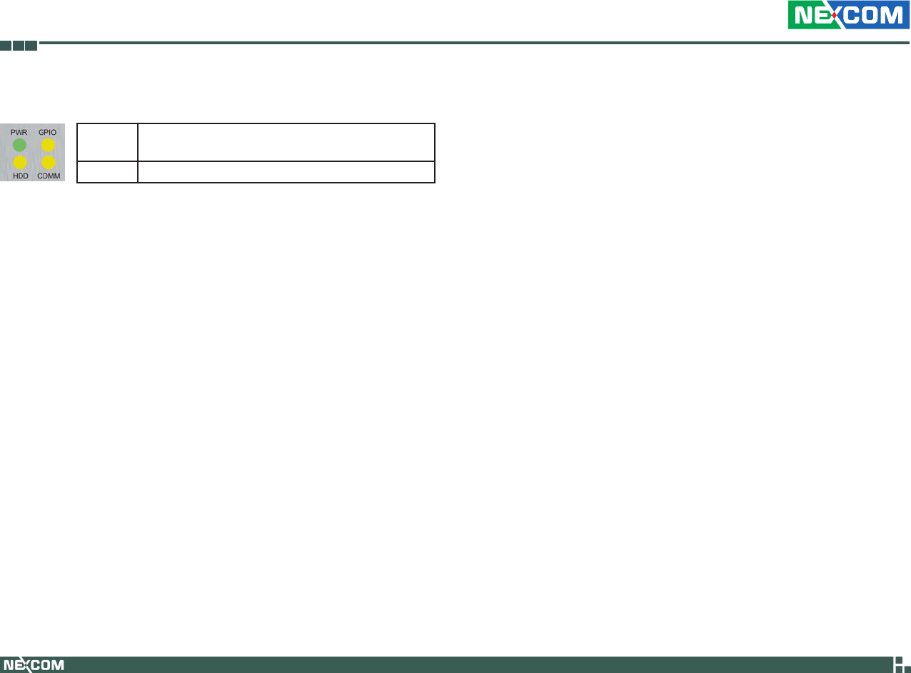
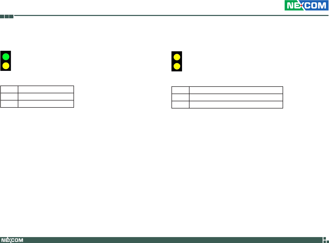
LEDs
GPIO I/O PORT Address : <Read/Write> #0EE0H Bit 0 :
0(Off) 1(On).
COMM WLAN/HSDPA Status
SIM Card Socket
VTC 6110 can be internally integrated with a 3.5G Mini Card module. The
SIM card bracket is on the carrier board. When using the GPRS/UMTS/HS-
DPA function, insert the SIM card into the SIM card socket. Make sure to
turn off VTC 6110 before inserting the SIM card.
USB Port
The USB port complies with USB 2.0 specifications.
WiFi/Bluetooth Module Antenna Mounting Holes
The 3 external antenna mounting holes are used to mount and connect
WiFi antenna to a WLAN module (Mini Card type).
GPRS/UMTS/HSDPA Module Antenna Mounting Hole
The antenna mounting hole is used to mount and connect an antenna to
the GPRS/UMTS/HSDPA module.
Reset Button
Press this button to restart VTC 6110.
Line-out
Line-out is a stereo output for connecting external speakers.
Mic-in
Mic-in receives monophonic input from an external microphone.
Copyright © 2009 NEXCOM International Co., Ltd. All Rights Reserved. 8VTC 6110 User Manual
Chapter 1: Product Introduction
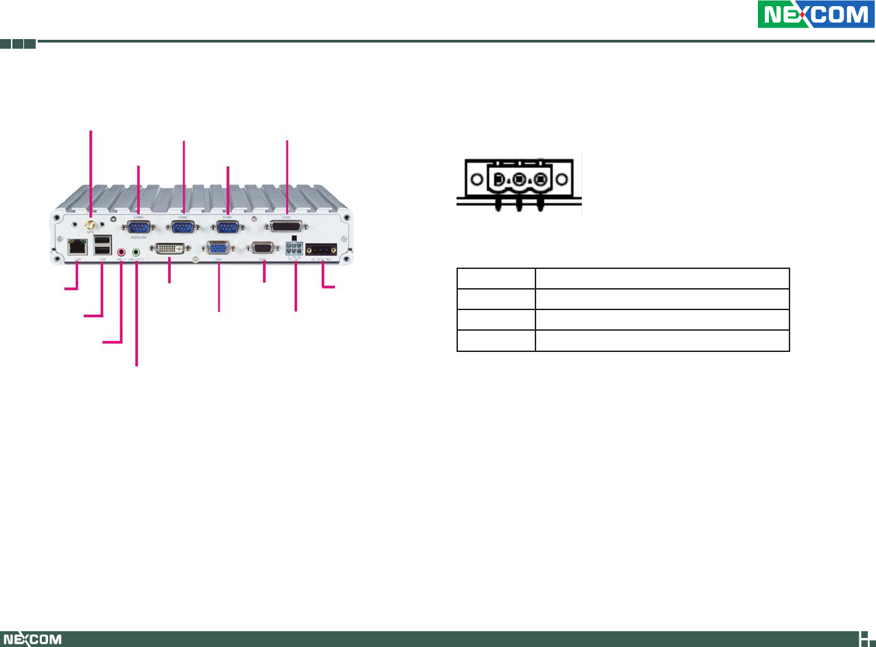
Rear Panel
** Use power cable (+) with fuse for system protection
Power Input
DC Power Input Connector
Connector location
3 2 1
Connector pin definition (CN1)
Pin No. Function Description
1 GND
2 VIN(6V~36V)
3 IGNITION
VGA
COM1
COM2
COM3
GPS
LAN
USB
MIC-IN
LINE-OUT
DVI-D GPIO
5V/12V/SMBUS
DC IN 6V-36V
LVDS
Copyright © 2009 NEXCOM International Co., Ltd. All Rights Reserved. 9VTC 6110 User Manual
Chapter 1: Product Introduction
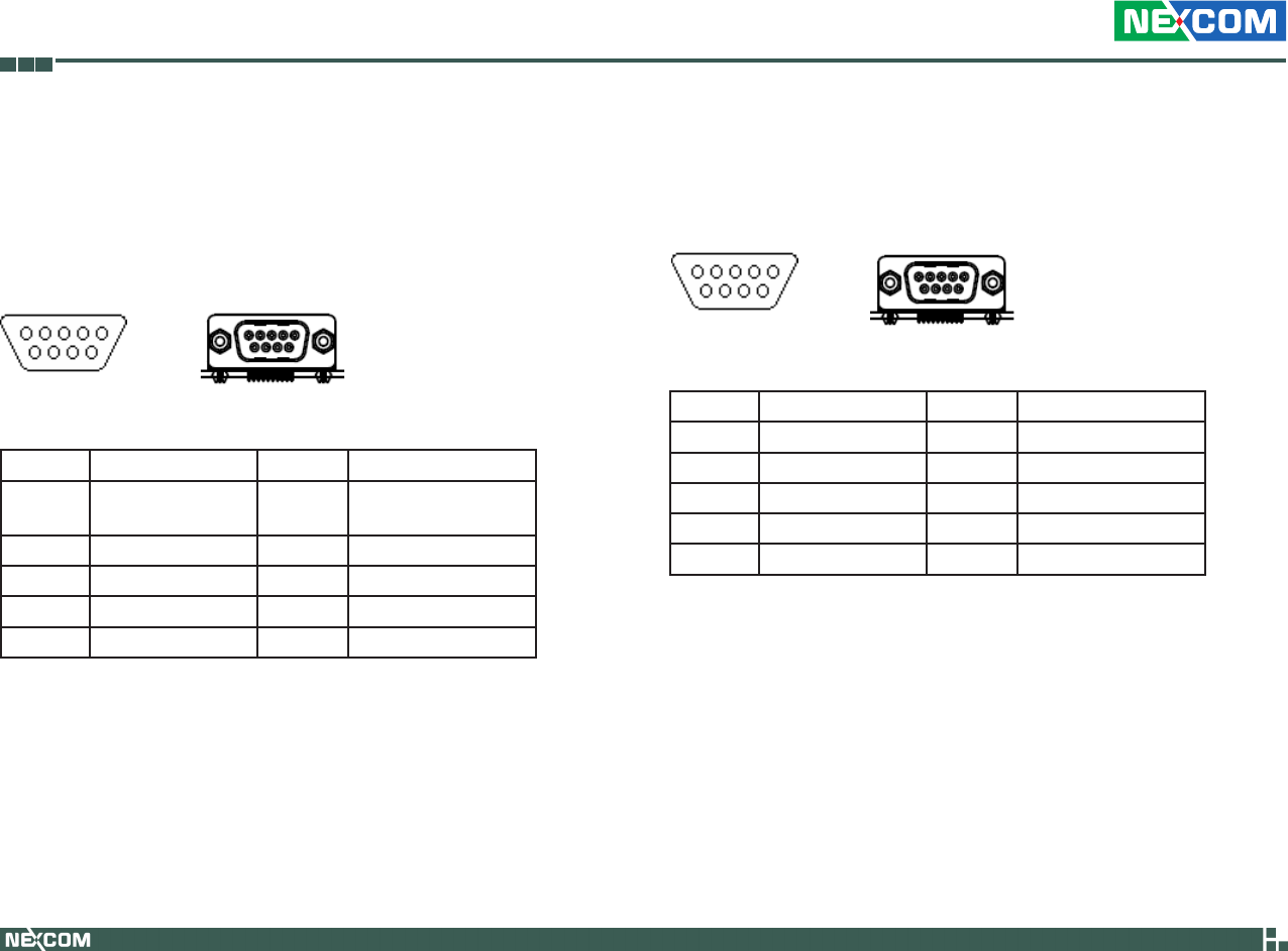
RS232/485 Connector COM3
The 9 pin D-Sub COM 3 port can be configured as RS232 or RS485 using
the SW6 dip switch.
Connector size: DSUB-9 PIN
Connector location
Connector pin definition
PIn Definition Pin Definition
1 DCD (RS232)
TX-/RX- (RS485)
2 RXD (RS232)
TX+/RX+ (RS485)
3 TXD (RS232) 4 DTR (RS232)
5 GND 6 DSR (RS232 )
7 RTS (RS232) 8 CTS (RS232)
9 RI (RS232)
RS232 Connector COM1 and COM2
Connector size: DSUB-9 PIN
Connector location
Connector pin definition
PIn Definition Pin Definition
1 DCD 2 RXD
3 TXD 4 DTR
5 GND 6 DSR
7 RTS 8 CTS
9 RI
1 5
6 9
1 5
6 9
Copyright © 2009 NEXCOM International Co., Ltd. All Rights Reserved. 10 VTC 6110 User Manual
Chapter 1: Product Introduction
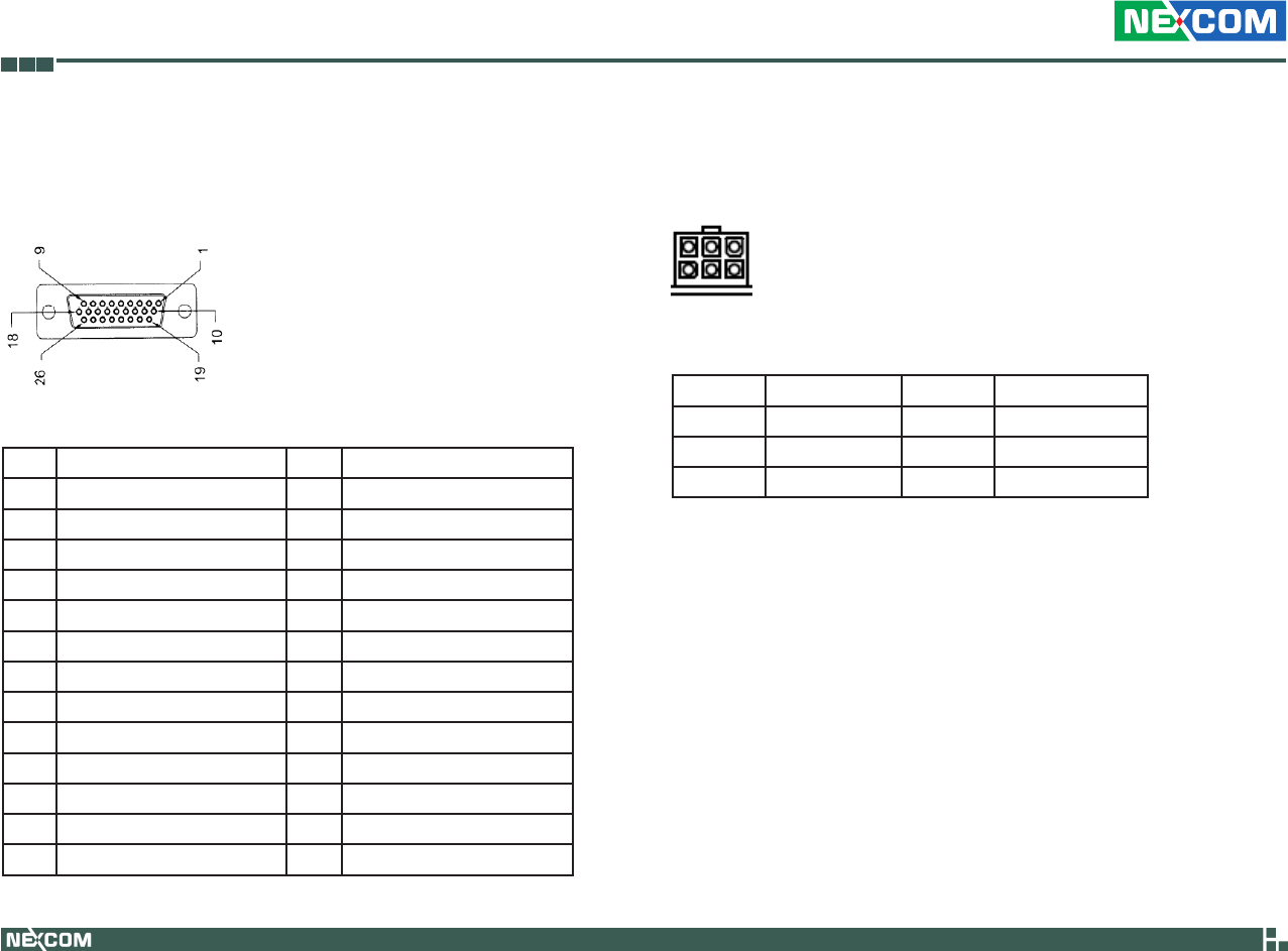
LVDS
Connector size: DB-26 PIN
Connector location
Connector pin definition
Pin Definition Pin Definition
1 Panel_ EN 2 Panel_control
3 VDD 4 VDD
5 LCDD09(OUT3) 6 LCDD01(OUT0)
7 LCDD08(OUT3#) 8 LCDD00(OUT0#)
9 LCDD_GND 10 LCDD_GND
11 LCDD07(CLK) 12 LCDD03(OUT1)
13 LCDD06(CLK#) 14 LCDD02(OUT1#)
15 LVDS_GND 16 LCDD_GND
17 LCDD05(OUT2) 18 Power on push button
19 LCDD04(OUT2#) 20 Panel_backlight
21 LCDD_GND 22 Panel-Gnd
23 USB_0# 24 Contact_DET#
25 USB_0 26 USB_VCC
External SMBus, 12V and 5V Power Output
Connector location
6 4
3 1
Connector pin definition
PIn Definition Pin Definition
1 5V 2 12V
3 SMBus Clock 4 GND
5 GND 6 SMBus Data
+5 VDC (1A) and +12VDC (1A) power output and SMBus
(w/o VTK 33M-01 connection)
+5 VDC (0.5A) and +12VDC (0.5A) power output and SMBus
(w/ VTK 33M-01 connection)

Copyright © 2009 NEXCOM International Co., Ltd. All Rights Reserved. 11 VTC 6110 User Manual
Chapter 1: Product Introduction
VGA Port
The DB15 VGA port supports resolutions up to 1600x1200 @ 85 Hz,
2048x1536 @ 60Hz.
USB Port x 2
The two USB ports are compliant with USB 2.0 specifications.
LAN Port
The LAN port is an RJ45 interface with integrated LEDs and supports
10/100/1000Mbps Ethernet data transfer rates.
Audio Jacks (MIC-IN and LINE-OUT)
MIC-IN jack receives monophonic input from an external microphone. •
LINE-OUT jack is the stereo output for connecting external speakers.•
Copyright © 2009 NEXCOM International Co., Ltd. All Rights Reserved. 12 VTC 6110 User Manual
Chapter 1: Product Introduction
Mechanical Dimensions
260.0
50.0
176.0

Copyright © 2009 NEXCOM International Co., Ltd. All Rights Reserved. 13
Chapter 2: Jumpers and Connectors
VTC 6110 User Manual
Ch a p t e r 2: Ju m p e r s a n d Co n n e C t o r s
This chapter describes how to set the jumpers on the motherboard. Note
that the following procedures are generic for all VTC 6110 series.
Before You Begin
Ensure you have a stable, clean working environment. Dust and dirt can •
get into components and cause a malfunction. Use containers to keep
small components separated.
Adequate lighting and proper tools can prevent you from accidentally •
damaging the internal components. Most of the procedures that follow
require only a few simple tools, including the following:
A Philips screwdriver •
A flat-tipped screwdriver •
A set of jewelers Screwdrivers •
A grounding strap •
An anti-static pad •
Using your fingers can disconnect most of the connections. It is recom-•
mended that you do not use needle-nosed pliers to disconnect connec-
tions as these can damage the soft metal or plastic parts of the connec-
tors.
Before working on internal components, make sure that the power •
is off. Ground yourself before touching any internal components, by
touching a metal object. Static electricity can damage many of the elec-
tronic components. Humid environment tend to have less static electric-
ity than dry environments. A grounding strap is warranted whenever
danger of static electricity exists.
Precautions
Computer components and electronic circuit boards can be damaged by
discharges of static electricity. Working on the computers that are still con-
nected to a power supply can be extremely dangerous.
Follow the guidelines below to avoid damage to your computer or your-
self:
Always disconnect the unit from the power outlet whenever you are •
working inside the case.
If possible, wear a grounded wrist strap when you are working inside •
the computer case. Alternatively, discharge any static electricity by
touching the bare metal chassis of the unit case, or the bare metal body
of any other grounded appliance.
Hold electronic circuit boards by the edges only. Do not touch the com-com-•
ponents on the board unless it is necessary to do so. Don’t flex or stress
the circuit board.
Leave all components inside the static-proof packaging that they •
shipped with until they are ready for installation.
Use correct screws and do not over tighten screws.•
Copyright © 2009 NEXCOM International Co., Ltd. All Rights Reserved. 14
Chapter 2: Jumpers and Connectors
VTC 6110 User Manual
Jumper
A jumper is the simplest kind of electric switch. It consists of two metal
pins and a cap. When setting the jumpers, ensure that the jumper caps are
placed on the correct pins. When the jumper cap is placed on both pins,
the jumper is short. If you remove the jumper cap, or place the jumper
cap on just one pin, the jumper is open.
Refer to the illustrations below for examples of what the 2-pin and 3-pin
jumpers look like when they are short (on) and open (off).
Two-Pin Jumpers: Open (Left) and Short (Right)
Three-Pin Jumpers: Pins 1 and 2 Are Short
Copyright © 2009 NEXCOM International Co., Ltd. All Rights Reserved. 15
Chapter 2: Jumpers and Connectors
VTC 6110 User Manual
Locations of the Jumpers and Connectors
VTCB6110
The figure on the right is the VTCB6110
carrier board which is the board used in
the VTC6110 system. It shows the loca-
tions of the jumpers and connectors.
CN4
CN17
10 1
J14
CN1
1
CN2
1
6
J5
COM1
30
29
2
1
CN3
CON1
J8
61
CN5
1 4
J10
SW6
1 7
CN6
1
2
9
10
CN7
1
9
10
CN9
1
2
9
10
CN12
USB2
LAN1
1
15
17
51
2
16
18
52
1
15
17
51
2
16
18
52
CN16
1
J12
CN8
4
CN11
1
CN14
2
6
CN15
5
2
1
6
29
21
13
5
BZ1
24
12
6
1
JP5
5
1
JP6
2
1
JP8
2
1
JP7
J7
10
1
3
1
3
1
J6
3
1
JP4
3
1
JP3
3
1
JP2
3
1
JP1
3
1
J1
SW1
J3
J4
LED1
LED2
USB1
SW7
SW2
SW3
SW4SW5
1
J11
1
J2
1
J9
41
Blue Tooth
WLAN
3.5G
J13
Copyright © 2009 NEXCOM International Co., Ltd. All Rights Reserved. 16
Chapter 2: Jumpers and Connectors
VTC 6110 User Manual
Jumper Settings
SW5 / Input
Voltage
12V (default) 24V 6V~36V
SW5.1 OFF OFF ON
SW5.2 OFF ON Ignore
SW5: Input Voltage Selection
SW6: COM Port Mode Selection
SW6 COM Port Mode RS232
(default)
RS485
SW6.1 OFF ON
SW6.2 OFF ON
SW6.3 OFF ON
CF (IDE0) Primary Master/Slave Select (JP4)
Pin Status Function Description
1-2 Short Slave
2-3 (default) Short (default) Master
LVDS Power Input Voltage Select (JP9)
Pin Status Function Description
1-2 Short +5V IN
2-3 (default) Short (default) +3.3V IN
CMOS Input Voltage Select (J6)
Pin Status Function Description
1-2 (default) Short (default) VBAT IN
2-3 Short Clear CMOS
BIOS Function Select (J1)
Pin Status Function Description
1-2 Short Disable carrier board BIOS
2-3 (default) Short (default) Disable module board BIOS
DC Input Voltage Select (JP1)
Pin Status Function Description
1-2 (default) Short (default) IGNITION
2-3 Short VIN_M
Copyright © 2009 NEXCOM International Co., Ltd. All Rights Reserved. 17
Chapter 2: Jumpers and Connectors
VTC 6110 User Manual
Temp Sensor (JP8)
Pin Function Description
1 SENSOR+
2 GND
Auto Power Select (JP2)
Pin Status Function Description
1-2 (default) Short (default) AUTO
2-3 Short BUTTON CONTROL
PCI-104 VI/O Select Voltage (J13)
Pin Status Function Description
1-4(*) Short* +3.3V
3-6 Short +5V
MCU Download (JP6)
Pin Function Description
1 +V3.3ALW
2 C2D
3 MRST
4 C2CK
5 GND
GAL Download (JP5)
Pin Function Description
1 +V3.3S
2 GND
3 TCK
4 TDO
5 TDI
6 TMS
MCU COM Port (JP3)
Pin Function Description
1 TX
2 RX
3 GND
Copyright © 2009 NEXCOM International Co., Ltd. All Rights Reserved. 18
Chapter 2: Jumpers and Connectors
VTC 6110 User Manual
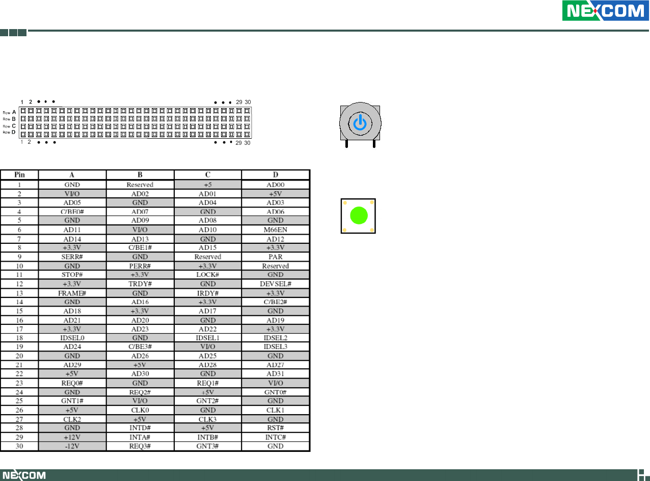
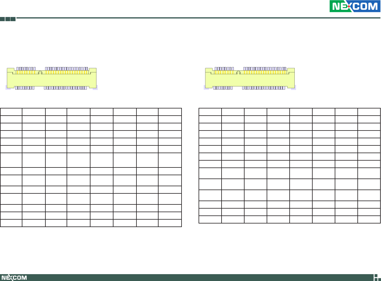
Connectors
High Speed Board-to-Board Connector:
COM Express Row A and Row B
Connector size: 2 x 110 = 220 pins
Connector location: J4
COM Express Connector
J1
COM Express
A1
A1
A2
A2
A3
A3
A4
A4
A5
A5
A6
A6
A7
A7
A8
A8
A9
A9
A10
A10
A11
A11
A12
A12
A13
A13
A14
A14
A15
A15
A16
A16
A17
A17
A18
A18
A19
A19
A20
A20
A21
A21
A22
A22
A23
A23
A24
A24
A25
A25
A26
A26
A27
A27
A28
A28
A29
A29
A30
A30
A31
A31
A32
A32
A33
A33
A34
A34
A35
A35
A36
A36
A37
A37
A38
A38
A39
A39
A40
A40
A41
A41
A42
A42
A43
A43
A44
A44
A45
A45
A46
A46
A47
A47
A48
A48
A49
A49
A50
A50
A51
A51
A52
A52
A53
A53
A54
A54
A55
A55
A56
A56
A57
A57
A58
A58
A59
A59
A60
A60
A61
A61
A62
A62
A63
A63
A64
A64
A65
A65
A66
A66
A67
A67
A68
A68
A69
A69
A70
A70
A71
A71
A72
A72
A73
A73
A74
A74
A75
A75
A76
A76
A77
A77
A78
A78
A79
A79
A80
A80
A81
A81
A82
A82
A83
A83
A84
A84
A85
A85
A86
A86
A87
A87
A88
A88
A89
A89
A90
A90
A91
A91
A92
A92
A93
A93
A94
A94
A95
A95
A96
A96
A97
A97
A98
A98
A99
A99
A100
A100
A101
A101
A102
A102
A103
A103
A104
A104
A105
A105
A106
A106
A107
A107
A108
A108
A109
A109
A110
A110
B1 B1
B2 B2
B3 B3
B4 B4
B5 B5
B6 B6
B7 B7
B8 B8
B9 B9
B10 B10
B11 B11
B12 B12
B13 B13
B14 B14
B15 B15
B16 B16
B17 B17
B18 B18
B19 B19
B20 B20
B21 B21
B22 B22
B23 B23
B24 B24
B25 B25
B26 B26
B27 B27
B28 B28
B29 B29
B30 B30
B31 B31
B32 B32
B33 B33
B34 B34
B35 B35
B36 B36
B37 B37
B38 B38
B39 B39
B40 B40
B41 B41
B42 B42
B43 B43
B44 B44
B45 B45
B46 B46
B47 B47
B48 B48
B49 B49
B50 B50
B51 B51
B52 B52
B53 B53
B54 B54
B55 B55
B56 B56
B57 B57
B58 B58
B59 B59
B60 B60
B61 B61
B62 B62
B63 B63
B64 B64
B65 B65
B66 B66
B67 B67
B68 B68
B69 B69
B70 B70
B71 B71
B72 B72
B73 B73
B74 B74
B75 B75
B76 B76
B77 B77
B78 B78
B79 B79
B80 B80
B81 B81
B82 B82
B83 B83
B84 B84
B85 B85
B86 B86
B87 B87
B88 B88
B89 B89
B90 B90
B91 B91
B92 B92
B93 B93
B94 B94
B95 B95
B96 B96
B97 B97
B98 B98
B99 B99
B100 B100
B101 B101
B102 B102
B103 B103
B104 B104
B105 B105
B106 B106
B107 B107
B108 B108
B109 B109
B110 B110
MH1 MH1
MH2 MH2
Connector Pin Definition
Row A Row B Row A Row B
A1 GND B1 GND A56 NC B56 NC
A2 GBE0_MDI3- B2 GBE0_ACT# A57 GND B57 NC
A3 GBE0_MDI3+ B3 LPC_FRAME# A58 NC B58 NC
A4 NC B4 LPC_AD0 A59 NC B59 NC
A5 NC B5 LPC_AD1 A60 GND B60 GND
A6 GBE0_MDI2- B6 LPC_AD2 A61 NC B61 NC
A7 GBE0_MDI2+ B7 LPC_AD3 A62 NC B62 NC
A8 GBE0_LINK# B8 NC A63 GPI1 B63 GPO3
A9 GBE0_MDI1- B9 NC A64 NC B64 NC
A10 GBE0_MDI1+ B10 LPC_CLK A65 NC B65 NC
A11 GND B11 GND A66 GND B66 NC
A12 GBE0_MDI0- B12 PWRBTN# A67 NC B67 NC
Row A Row B Row A Row B
A13 GBE0_MDI0+ B13 SMB_CK A68 PCIE_TX0+ B68 PCIE_RX0+
A14 GBE0_CTREF B14 SMB_DAT A69 PCIE_TX0- B69 PCIE_RX0-
A15 SUS_S3# B15 SMB_ALERT# A70 GND B70 GND
A16 SATA0_TX+ B16 NC A71 LVDS_A0+ B71 NC
A17 SATA0_TX- B17 NC A72 LVDS_A0- B72 NC
A18 SUS_S4# B18 SUS_STAT# A73 LVDS_A1+ B73 NC
A19 SATA0_RX+ B19 NC A74 LVDS_A1+ B74 NC
A20 SATA0_RX- B20 NC A75 LVDS_A2+ B75 NC
A21 GND B21 GND A76 LVDS_A2+ B76 NC
A22 NC B22 NC A77 LVDS_VDD_EN B77 NC
A23 NC B23 NC A78 LVDS_A3+ B78 NC
A24 SUS_S5# B24 PWR_OK A79 LVDS_A3+ B79 LVDS_BKLT_EN
A25 NC B25 NC A80 GND B80 GND
A26 NC B26 NC A81 LVDS_A_CK+ B81 NC
A27 BATLOW# B27 NC A82 LVDS_A_CK- B82 NC
A28 ATA_ACT# B28 NC A83 LVDS_I2C_CK B83 LVDS_BKLT_
CTRL
A29 AC_SYNC B29 NC A84 LVDS_I2C_DAT B84 VCC_5V_SBY
A30 AC_RST# B30 AC_SDIN0 A85 NC B85 VCC_5V_SBY
A31 GND B31 GND A86 NC B86 VCC_5V_SBY
A32 AC_BITCLK B32 SPKR A87 NC B87 VCC_5V_SBY
A33 AC_SDOUT B33 I2C_CK A88 PCIE0_CK_REF+ B88 RSVD
A34 NC B34 I2C_DAT A89 PCIE0_CK_REF- B89 NC
A35 NC B35 THRM# A90 GND B90 GND
A36 USB6- B36 NC A91 RSVD B91 NC
A37 USB6+ B37 NC A92 RSVD B92 NC
A38 USB_6_7_OC# B38 USB_4_5_OC# A93 NC B93 NC
A39 USB4- B39 USB5- A94 RSVD B94 NC
Row B
Row A

Copyright © 2009 NEXCOM International Co., Ltd. All Rights Reserved. 19
Chapter 2: Jumpers and Connectors
VTC 6110 User Manual
Row A Row B Row A Row B
A40 USB4+ B40 USB5+ A95 RSVD B95 NC
A41 GND B41 GND A96 GND B96 NC
A42 USB2- B42 USB3- A97 VCC_12V B97 NC
A43 USB2+ B43 USB3+ A98 VCC_12V B98 NC
A44 USB_2_3_OC# B44 USB_0_1_OC# A99 VCC_12V B99 NC
A45 USB0- B45 USB1- A100 GND B100 GND
A46 USB0+ B46 USB1+ A101 VCC_12V B101 VCC_12V
A47 VCC_RTC B47 NC A102 VCC_12V B102 VCC_12V
A48 NC B48 NC A103 VCC_12V B103 VCC_12V
A49 NC B49 SYS_RESET# A104 VCC_12V B104 VCC_12V
A50 NC B50 CB_RESET# A105 VCC_12V B105 VCC_12V
A51 GND B51 GND A106 VCC_12V B106 VCC_12V
A52 NC B52 NC A107 VCC_12V B107 VCC_12V
A53 NC B53 NC A108 VCC_12V B108 VCC_12V
A54 NC B54 NC A109 VCC_12V B109 VCC_12V
A55 NC B55 NC A110 GND B110 GND
Copyright © 2009 NEXCOM International Co., Ltd. All Rights Reserved. 20
Chapter 2: Jumpers and Connectors
VTC 6110 User Manual
High Speed Board-to-Board Connector:
COM Express Row C and Row D
Connector size: 2 X 110 = 220 Pins
Connector location: J3
COM Express Connector
J1
COM Express
A1
A1
A2
A2
A3
A3
A4
A4
A5
A5
A6
A6
A7
A7
A8
A8
A9
A9
A10
A10
A11
A11
A12
A12
A13
A13
A14
A14
A15
A15
A16
A16
A17
A17
A18
A18
A19
A19
A20
A20
A21
A21
A22
A22
A23
A23
A24
A24
A25
A25
A26
A26
A27
A27
A28
A28
A29
A29
A30
A30
A31
A31
A32
A32
A33
A33
A34
A34
A35
A35
A36
A36
A37
A37
A38
A38
A39
A39
A40
A40
A41
A41
A42
A42
A43
A43
A44
A44
A45
A45
A46
A46
A47
A47
A48
A48
A49
A49
A50
A50
A51
A51
A52
A52
A53
A53
A54
A54
A55
A55
A56
A56
A57
A57
A58
A58
A59
A59
A60
A60
A61
A61
A62
A62
A63
A63
A64
A64
A65
A65
A66
A66
A67
A67
A68
A68
A69
A69
A70
A70
A71
A71
A72
A72
A73
A73
A74
A74
A75
A75
A76
A76
A77
A77
A78
A78
A79
A79
A80
A80
A81
A81
A82
A82
A83
A83
A84
A84
A85
A85
A86
A86
A87
A87
A88
A88
A89
A89
A90
A90
A91
A91
A92
A92
A93
A93
A94
A94
A95
A95
A96
A96
A97
A97
A98
A98
A99
A99
A100
A100
A101
A101
A102
A102
A103
A103
A104
A104
A105
A105
A106
A106
A107
A107
A108
A108
A109
A109
A110
A110
B1 B1
B2 B2
B3 B3
B4 B4
B5 B5
B6 B6
B7 B7
B8 B8
B9 B9
B10 B10
B11 B11
B12 B12
B13 B13
B14 B14
B15 B15
B16 B16
B17 B17
B18 B18
B19 B19
B20 B20
B21 B21
B22 B22
B23 B23
B24 B24
B25 B25
B26 B26
B27 B27
B28 B28
B29 B29
B30 B30
B31 B31
B32 B32
B33 B33
B34 B34
B35 B35
B36 B36
B37 B37
B38 B38
B39 B39
B40 B40
B41 B41
B42 B42
B43 B43
B44 B44
B45 B45
B46 B46
B47 B47
B48 B48
B49 B49
B50 B50
B51 B51
B52 B52
B53 B53
B54 B54
B55 B55
B56 B56
B57 B57
B58 B58
B59 B59
B60 B60
B61 B61
B62 B62
B63 B63
B64 B64
B65 B65
B66 B66
B67 B67
B68 B68
B69 B69
B70 B70
B71 B71
B72 B72
B73 B73
B74 B74
B75 B75
B76 B76
B77 B77
B78 B78
B79 B79
B80 B80
B81 B81
B82 B82
B83 B83
B84 B84
B85 B85
B86 B86
B87 B87
B88 B88
B89 B89
B90 B90
B91 B91
B92 B92
B93 B93
B94 B94
B95 B95
B96 B96
B97 B97
B98 B98
B99 B99
B100 B100
B101 B101
B102 B102
B103 B103
B104 B104
B105 B105
B106 B106
B107 B107
B108 B108
B109 B109
B110 B110
MH1 MH1
MH2 MH2
Row D
Row C
Connector Pin Definition
Row C Row D Row C Row D
C1 GND D1 GND C56 NC D56 SDVOB_GREEN-
C2 IDE_D7 D2 IDE_D5 C57 NC D57 NC
C3 IDE_D6 D3 IDE_D10 C58 NC D58 SDVOB_BLUE+
C4 IDE_D3 D4 IDE_D11 C59 NC D59 SDVOB_BLUE-
C5 IDE_D15 D5 IDE_D12 C60 GND D60 GND
C6 IDE_D8 D6 IDE_D4 C61 NC D61 SDVO_CLK+
C7 IDE_D9 D7 IDE_D0 C62 NC D62 SDVO_CLK-
C8 IDE_D2 D8 IDE_REQ C63 NC D63 NC
C9 IDE_D13 D9 IDE_IOW# C64 NC D64 NC
C10 IDE_D1 D10 IDE_ACK# C65 NC D65 NC
C11 GND D11 GND C66 NC D66 NC
C12 IDE_D14 D12 IDE_IRQ C67 NC D67 GND
Row C Row D Row C Row D
C13 IDE_IORDY D13 IDE_A0 C68 NC D68 NC
C14 IDE_IOR# D14 IDE_A1 C69 NC D69 NC
C15 NC D15 IDE_A2 C70 GND D70 GND
C16 NC D16 IDE_CS1# C71 NC D71 NC
C17 NC D17 IDE_CS3# C72 NC D72 NC
C18 NC D18 IDE_RESET# C73 NC D73 SDVO_CLK
C19 NC D19 NC C74 NC D74 NC
C20 PCI_GNT0# D20 NC C75 NC D75 NC
C21 GND D21 GND C76 GND D76 GND
C22 PCI_REQ0# D22 PCI_AD1 C77 NC D77 IDE_CBLID#
C23 PCI_RESET# D23 PCI_AD3 C78 NC D78 NC
C24 PCI_AD0 D24 PCI_AD5 C79 NC D79 NC
C25 PCI_AD2 D25 PCI_AD7 C80 GND D80 GND
C26 PCI_AD4 D26 PCI_C/BE0# C81 NC D81 NC
C27 PCI_AD6 D27 PCI_AD9 C82 NC D82 NC
C28 PCI_AD8 D28 PCI_AD11 C83 NC D83 NC
C29 PCI_AD10 D29 PCI_AD13 C84 GND D84 GND
C30 PCI_AD12 D30 PCI_AD15 C85 NC D85 NC
C31 GND D31 GND C86 NC D86 NC
C32 PCI_AD14 D32 PCI_PAR C87 GND D87 GND
C33 PCI_C/BE1# D33 PCI_SERR# C88 NC D88 NC
C34 PCI_PERR# D34 PCI_STOP# C89 NC D89 NC
C35 PCI_LOCK# D35 PCI_TRDY# C90 GND D90 GND
C36 PCI_DEVSEL# D36 PCI_FRAME# C91 NC D91 NC
C37 PCI_IRDY# D37 PCI_AD16 C92 NC D92 NC
C38 PCI_C/BE2# D38 PCI_AD18 C93 GND D93 GND
C39 PCI_AD17 D39 PCI_AD20 C94 NC D94 NC
Copyright © 2009 NEXCOM International Co., Ltd. All Rights Reserved. 21
Chapter 2: Jumpers and Connectors
VTC 6110 User Manual
Row C Row D Row C Row D
C40 PCI_AD19 D40 PCI_AD22 C95 PEG_RX13- D95 PEG_TX13-
C41 GND D41 GND C96 GND D96 GND
C42 PCI_AD21 D42 PCI_AD24 C97 RSVD D97 PEG_ENABLE#
C43 PCI_AD23 D43 PCI_AD26 C98 PEG_RX14+ D98 PEG_TX14+
C44 PCI_C/BE3# D44 PCI_AD28 C99 PEG_RX14- D99 PEG_TX14-
C45 PCI_AD25 D45 PCI_AD30 C100 GND D100 GND
C46 PCI_AD27 D46 PCI_IRQC# C101 PEG_RX15+ D101 PEG_TX15+
C47 PCI_AD29 D47 PCI_IRQD# C102 PEG_RX15- D102 PEG_TX15-
C48 PCI_AD31 D48 PCI_CLKRUN# C103 GND D103 GND
C49 PCI_IRQA# D49 PCI_M66EN C104 VCC_12V D104 VCC_12V
C50 PCI_IRQB# D50 PCI_CLK C105 VCC_12V D105 VCC_12V
C51 GND D51 GND C106 VCC_12V D106 VCC_12V
C52 PEG_RX0+ D52 PEG_TX0+ C107 VCC_12V D107 VCC_12V
C53 PEG_RX0- D53 PEG_TX0- C108 VCC_12V D108 VCC_12V
C54 TYPE0# D54 PEG_LANE_RV# C109 VCC_12V D109 VCC_12V
C55 PEG_RX1+ D55 PEG_TX1+ C110 GND D110 GND
Copyright © 2009 NEXCOM International Co., Ltd. All Rights Reserved. 22
Chapter 2: Jumpers and Connectors
VTC 6110 User Manual
CompactFlash Connector
Connector size: 2 x 25 = 50 pins
Connector location: J12
1
26
50
49
Pin Description Pin Description
1 Gnd 2 Data 3
3 Data 4 4 Data 5
5 Data 6 6 Data 7
7 HDC CS100 8 Gnd
9 Gnd 10 Gnd
11 Gnd 12 Gnd
13 +5V 14 Gnd
15 Gnd 16 Gnd
17 Gnd 18 Disk Address 2
19 Disk Address 1 20 Disk Address 0
21 Data 0 22 Data 1
Connector Pin Definition
Pin Description Pin Description
23 Data 2 24 IOCS16# (NC)
25 CF_CD2# (Pull-down) 26 CF_CD1# (Pull-down)
27 Data 11 28 Data 12
29 Data 13 30 Data 14
31 Data 15 32 HDC CS300
33 CF_VS1# (NC) 34 IOR
35 IOW 36 CF_WE# (+5V)
37 Interrupt 15 38 +5V
39 CF_CSEL# (Master or Slave) 40 CF_VS2# (NC)
41 Reset # 42 IOCHRDY
43 DMA REQ / DACK (NC) 44 DMA ACK# /CF_REG# (+5V)
45 HDD Active Led 46 DMA66 Detect / CF_PDIAG#
47 Data 8 48 Data 9
49 Data 10 50 Gnd
Copyright © 2009 NEXCOM International Co., Ltd. All Rights Reserved. 23
Chapter 2: Jumpers and Connectors
VTC 6110 User Manual
GPIO Connector
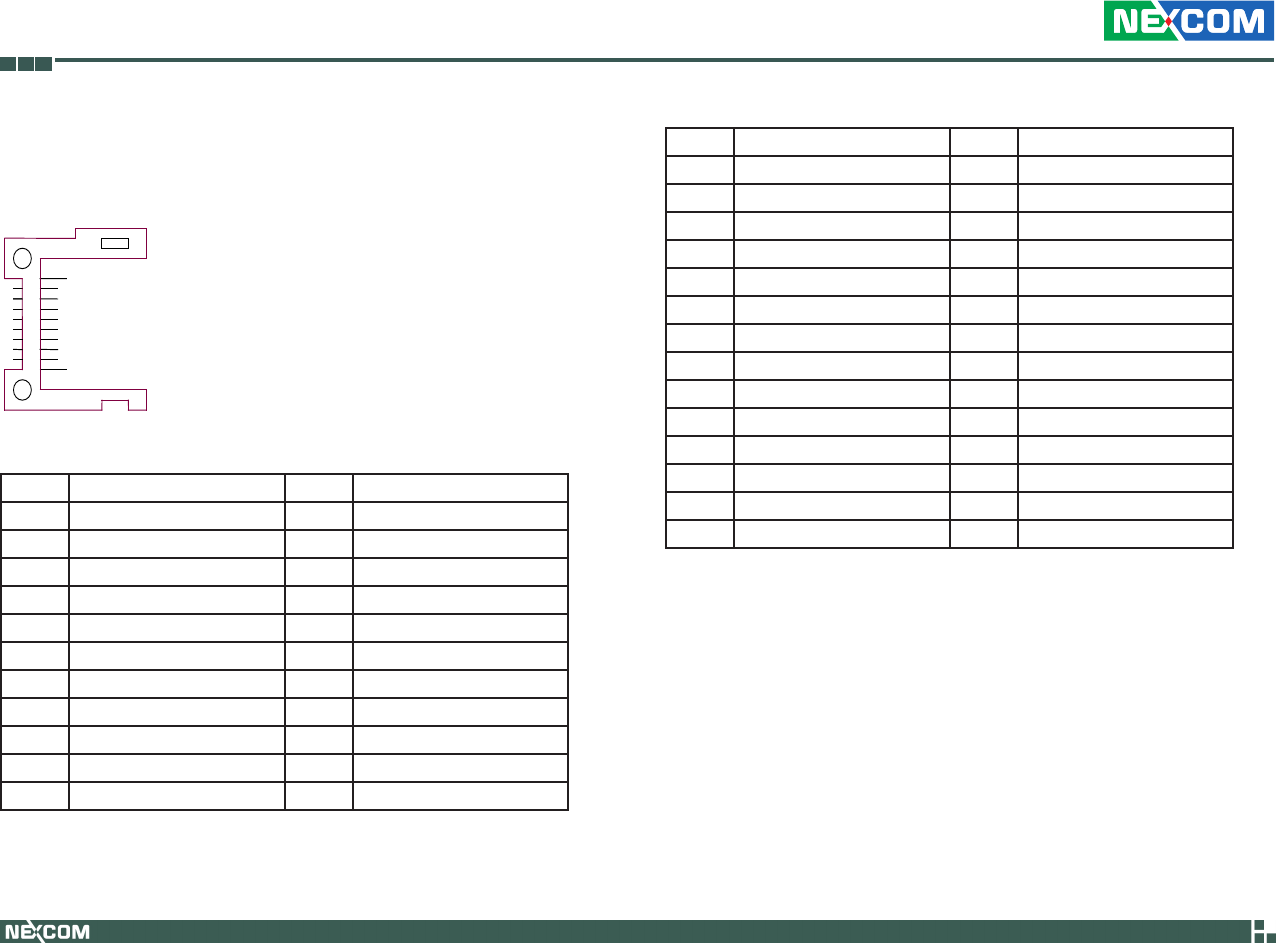
Connector size: DSUB-9 pin
Connector location: COM1
Pin Description Pin Description
1 GIN1 2 GIN2
3 GIN3 4 GIN4
5 GOUT4 6 GOUT1
7 GOUT2 8 GOUT3
9 GND
Connector Pin Definition
5 1
9 6
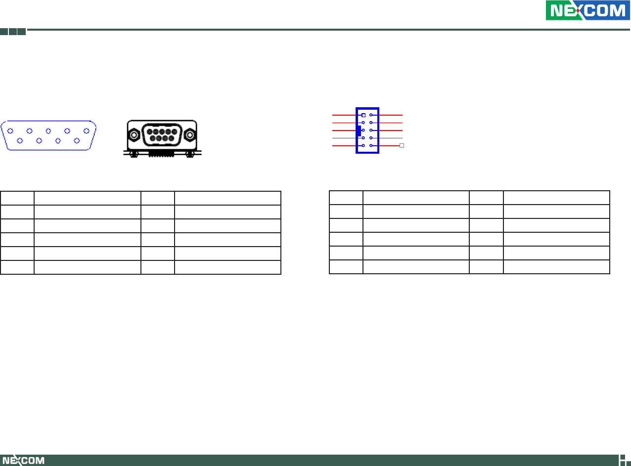
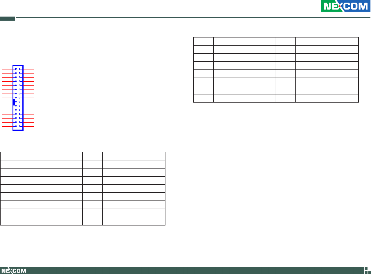
RS232 Connector: COM1, COM2
Connector size: 2 x 10 = 20 Pins Pin Header, (2.0 mm Pitch)
Connector location: COM1 (CN9), COM2 (CN7)
CN10
BOX-2.0mm-M-180
1
3 4
2
5 6
7 8
910
Connector Pin Definition
Pin Definition Pin Definition
1 DCD 2 RXD
3 TXD 4 DTR
5 Gnd 6 DSR
7 RTS 8 CTS
9 RI
Copyright © 2009 NEXCOM International Co., Ltd. All Rights Reserved. 24
Chapter 2: Jumpers and Connectors
VTC 6110 User Manual
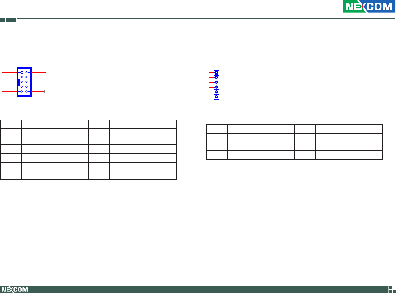
RS232/485 Connector: COM3
Connector size: 2 x 10 = 20 Pins Pin Header, (2.0 mm Pitch)
Connector location: CN12
CN10
BOX-2.0mm-M-180
1
3 4
2
5 6
7 8
910
Connector Pin Definition
Pin Definition Pin Definition
1 DCD (RS232)
TX-/RX- (RS485)
2 RXD (RS232)
TX+/RX+ (RS485)
3 TXD (RS232) 4 DTR (RS232)
5 Gnd 6 DSR (RS232)
7 RTS (RS232) 8 CTS (RS232)
9 RI (RS232)
GAL Programmer PIN Header
Connector size: 2.54mm-M-180
Connector location: JP5
JP5
PIN-2.54mm-M-180
1
2
3
4
5
6
Connector Pin Definition
Pin Definition Pin Definition
1 +3.3V 2 GND
3 TCK 4 TDO
5 TDI 6 TMS
Copyright © 2009 NEXCOM International Co., Ltd. All Rights Reserved. 25
Chapter 2: Jumpers and Connectors
VTC 6110 User Manual
MCU Programmer Pin Header
Connector size: 2.54mm-M-180
Connector location: JP6
JP6
PIN-2.54mm-M-180
1
2
3
4
5
Connector Pin Definition
Pin Definition Pin Definition
1 +3.3ALW 2 C2D
3 MRST 4 C2CK
5 GND
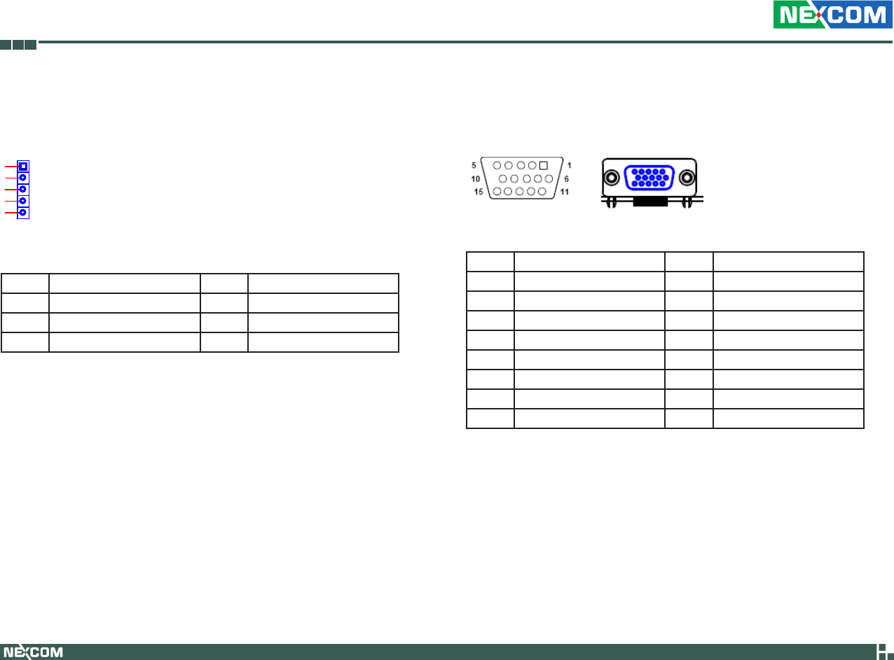
VGA Connector
Connector size: DSUB-15
Connector location: CON1
Connector Pin Definition
Pin Definition Pin Definition
1 RED 2 GREEN
3 BLUE 4 NC
5 Gnd 6 Gnd
7 Gnd 8 Gnd
9 VCC 10 Gnd
11 NC 12 DDCDAT
13 Hsync 14 Vsync
15 DDCCLK
Copyright © 2009 NEXCOM International Co., Ltd. All Rights Reserved. 26
Chapter 2: Jumpers and Connectors
VTC 6110 User Manual
LVDS Connector + USB0
Connector size: 2 x 15 (2.0mm)
Connector location: CN3
CN3
BOX-2.0mm-M-180
1
3 4
2
5 6
7 8
9
11 10
12
13 14
1615
17 18
20
22
24
26
28
30
21
23
25
27
29
19
Connector Pin Definition
Pin Definition Pin Definition
1 LVDS_CLK 2 LVDS_DAT
3 Panel_VDD 4 LVDS_1(OUT0)
5 LVDS_9(OUT3) 6 LVDS_0(OUT0#)
7 LVDS_8(OUT3#) 8 Panel_VDD
9 LVDS_GND 10 LVDS_GND
11 LVDS_7(CLK) 12 LVDS_3(OUT1)
13 LVDS_6(CLK#) 14 LVDS_2(OUT1#)
15 LVDS_GND 16 LVDS_GND
Pin Definition Pin Definition
17 LVDS_5(OUT2) 18 Panel_backlight(+12V)
19 LVDS_4(OUT2#) 20 Panel_backlight(+12V)
21 LVDS_GND 22 Power on push buttom
23 USB_0# 24 Contact_DET#
25 USB_0 26 USB_VCC (+5V)
27 USB_GND 28 USB_GND
29 Panel_backlight(+12V) 30 GND
Copyright © 2009 NEXCOM International Co., Ltd. All Rights Reserved. 27
Chapter 2: Jumpers and Connectors
VTC 6110 User Manual
LAN Connector
Connector size: RJ-45
Connector location: LAN1
Connector Pin Definition
Pin Definition Pin Definition
1 TX+ 2 TX-
3 RX+ 4 N/C1
5 N/C2 6 RX-
7 N/C3 8 N/C4
9 LAN Speed LED 10 +3.3V
11 LAN Link LED 12 +3.3V
USB Connector
Connector location: USB1
Connector Pin Definition
Pin Definition Pin Definition
1 VCC 2 DATA-
3 DATA+ 4 GND
Copyright © 2009 NEXCOM International Co., Ltd. All Rights Reserved. 28
Chapter 2: Jumpers and Connectors
VTC 6110 User Manual
Connector Pin Definition
Pin Definition Pin Definition
1 VCC 2 DATA1-
3 DATA1+ 4 GND
5 VCC 6 DATA-
7 DATA+ 8 GND
USB Connector
Connector location: USB2
LVDS Power Connector
Connector location: J5
1
Connector Pin Definition
Pin Definition Pin Definition
1 Panel_backlight 2 Panel_VDD
3 GND 4 GND
5 LVDS_PANEL 6 LVDS_BIASON
Copyright © 2009 NEXCOM International Co., Ltd. All Rights Reserved. 29
Chapter 2: Jumpers and Connectors
VTC 6110 User Manual
External 12V & 5V Power and SMBUS Connector
Connector location: CN2
6
3
4
1
Connector Pin Definition
Pin Definition Pin Definition
1 5V 2 12V
3 SMBCLK 4 GND
5 GND 6 SMBDATA
Mic-in
Connector location: CN11 and CN15
Connector Pin Definition
Pin Definition Pin Definition
1 NC 2 MIC_JD
3 NC 4 MIC_OUT
5 GND 6 GND
Copyright © 2009 NEXCOM International Co., Ltd. All Rights Reserved. 30
Chapter 2: Jumpers and Connectors
VTC 6110 User Manual
Line-out
Connector location: CN8 and CN14
Connector Pin Definition
Pin Definition Pin Definition
1 LINE_OUT_L 2 SURR_JD
3 NC 4 LINE_OUT_R
5 GND 6 GND
PCI-104 VI/O Voltage Setting
Connector location: J13
Connector Pin Definition
Pin No. Status Function Description
1-3, 2-4 (default) Short +3.3V
3-5, 4-6 Short +5V
4 62
3 51
Copyright © 2009 NEXCOM International Co., Ltd. All Rights Reserved. 31
Chapter 2: Jumpers and Connectors
VTC 6110 User Manual
PCI-104 Connector
Connector location: CN16
Connector Pin Definition
Power Button
Connector location: SW1
Reset Button
Connector location: SW2
Copyright © 2009 NEXCOM International Co., Ltd. All Rights Reserved. 32
Chapter 2: Jumpers and Connectors
VTC 6110 User Manual
MCU COM Port
Connector location: JP3
Connector Pin Definition
Pin Function Description
1 TX
2 RX
3 GND
ACC_ON LED
Connector location: JP7
1
Connector Pin Definition
Pin Function Description
1 +3.3V LED
2 GND
Copyright © 2009 NEXCOM International Co., Ltd. All Rights Reserved. 33
Chapter 2: Jumpers and Connectors
VTC 6110 User Manual
Temp Sensor
Connector location: JP8
1
Connector Pin Definition
Pin Function Description
1 SENSOR+
2 GND
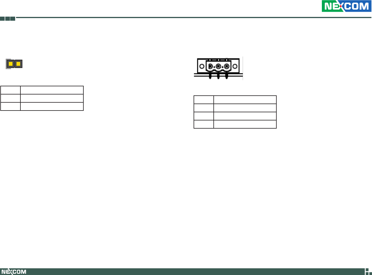
DC Power Input Connector
Connector location: CN1
Connector Pin Definition
Pin Function Description
1 GND
2 VIN (6V~36V)
3 IGNITION
Copyright © 2009 NEXCOM International Co., Ltd. All Rights Reserved. 34
Chapter 2: Jumpers and Connectors
VTC 6110 User Manual
Power On and IDE Active LED
Connector location: LED1
T1
B1
Connector Pin Definition
LED Function Description
T1 POWER LED
B1 HD LED
GPIO and UMTS LEDs
Connector location: LED2
T2
B2
LED I/O Port Address and Data
LED Function Description
T2 I/O PORT Address: 0EE0; Bit0: 1 (Light), 0 (Dark)
B2 UMTS STATUS
Copyright © 2009 NEXCOM International Co., Ltd. All Rights Reserved. 35
Chapter 2: Jumpers and Connectors
VTC 6110 User Manual
Serial ATA
Connector location: CN6
17
Connector Pin Definition
Pin Definition Pin Definition
1 GND 2 SATA_TXP0 -
3 SATA_TXN0 4 GND
5 SATA_RXN0 6 SATA_RXP0
7 GND
Serial ATA Power Input
Connector location: J10
1
4
Connector Pin Definition
Pin Definition Pin Definition
1 +V12S 2 GND
3 GND 4 +V5S
Copyright © 2009 NEXCOM International Co., Ltd. All Rights Reserved. 36
Chapter 2: Jumpers and Connectors
VTC 6110 User Manual
Mini-PCIe Socket (for 3.5G module)
PCIe Interface
Connector location: CN10
1
2
51
52
Connector Pin Definition
Pin Definition Pin Definition Pin Definition Pin Definition
1 MIC + 2 +V3.3S 27 GND 28 NC
3 MIC - 4 GND 29 GND 30 NC
5 SPK + 6 NC 31 NC 32 NC
7 GND 8 USIM PWR 33 RESET 34 GND
9 GND 10 USIM DATa 35 GND 36 USB_D-
11 VCC_
MSM26_
DIG
12 USIM CLK 37 GND 38 USB_D+
13 NC 14 USIM RST 39 +V3.3S 40 GND
15 GND 16 NC 41 +V3.3S 42 LED_
WWAN#
17 NC 18 GND 43 GND 44 NC
19 NC 20 W_DIS-
ABLE#
45 NC 46 NC
21 GND 22 NC 47 NC 48 NC
23 NC 24 NC 49 NC 50 GND
25 NC 26 GND 51 NC 52 +V3.3S
Mini-PCIe Socket (for WLAN module)
USB + PCIe Interface
Connector location: CN13
1
2
51
52
Connector Pin Definition
Pin Definition Pin Definition Pin Definition Pin Definition
1 WAKE# 2 +V3.3S 27 GND 28 +V1.5S
3 NC 4 GND 29 GND 30 SMB_CLK
5 NC 6 +V1.5S 31 PETn0 32 SMB_DATA
7 CLKREQ# 8 NC 33 PETp0 34 GND
9 GND 10 NC 35 GND 36 USB_D-
11 REFCLK- 12 NC 37 NC 38 USB_D+
13 REFCLK+ 14 NC 39 NC 40 GND
15 GND 16 NC 41 NC 42 LED_
WWAN#
17 NC 18 GND 43 NC 44 LED_
WLAN#
19 NC 20 DISABLE# 45 NC 46 LED_
WPAN#
21 GND 22 PERST# 47 NC 48 +V1.5S
23 PERn0 24 +3.3S 49 NC 50 GND
25 PERp0 26 GND 51 NC 52 +V3.3S
Copyright © 2009 NEXCOM International Co., Ltd. All Rights Reserved. 37
Chapter 2: Jumpers and Connectors
VTC 6110 User Manual
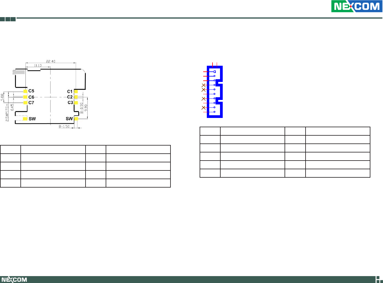
SIM Card Connector
Connector location: CN4
Connector Pin Definition
Pin Definition Pin Definition
C1 POWER VOLTAGE C2 RESET SIGNAL
C3 CLOCK SIGNAL C5 GND
C6 VPP:PROGRAM VOLTAGE C7 I/O
SW Contact present switch
Bluetooth Connector
Connector location: J7
J7
JST-1mm-M-90
1
2
3
MH1
MH2
4
5
6
10
9
8
7
Pin Definition Pin Definition
1 GND 2 USB_6P_L
3 USB_6N_L 4 NC
5 NC 6 BT_AUDIO_EN_R
7 NC 8 BT_3.3V
9 NC 10 GND
Copyright © 2009 NEXCOM International Co., Ltd. All Rights Reserved. 38
Chapter 3: System Setup
VTC 6110 User Manual
Ch a p t e r 3: Sy S t e m Se t u p
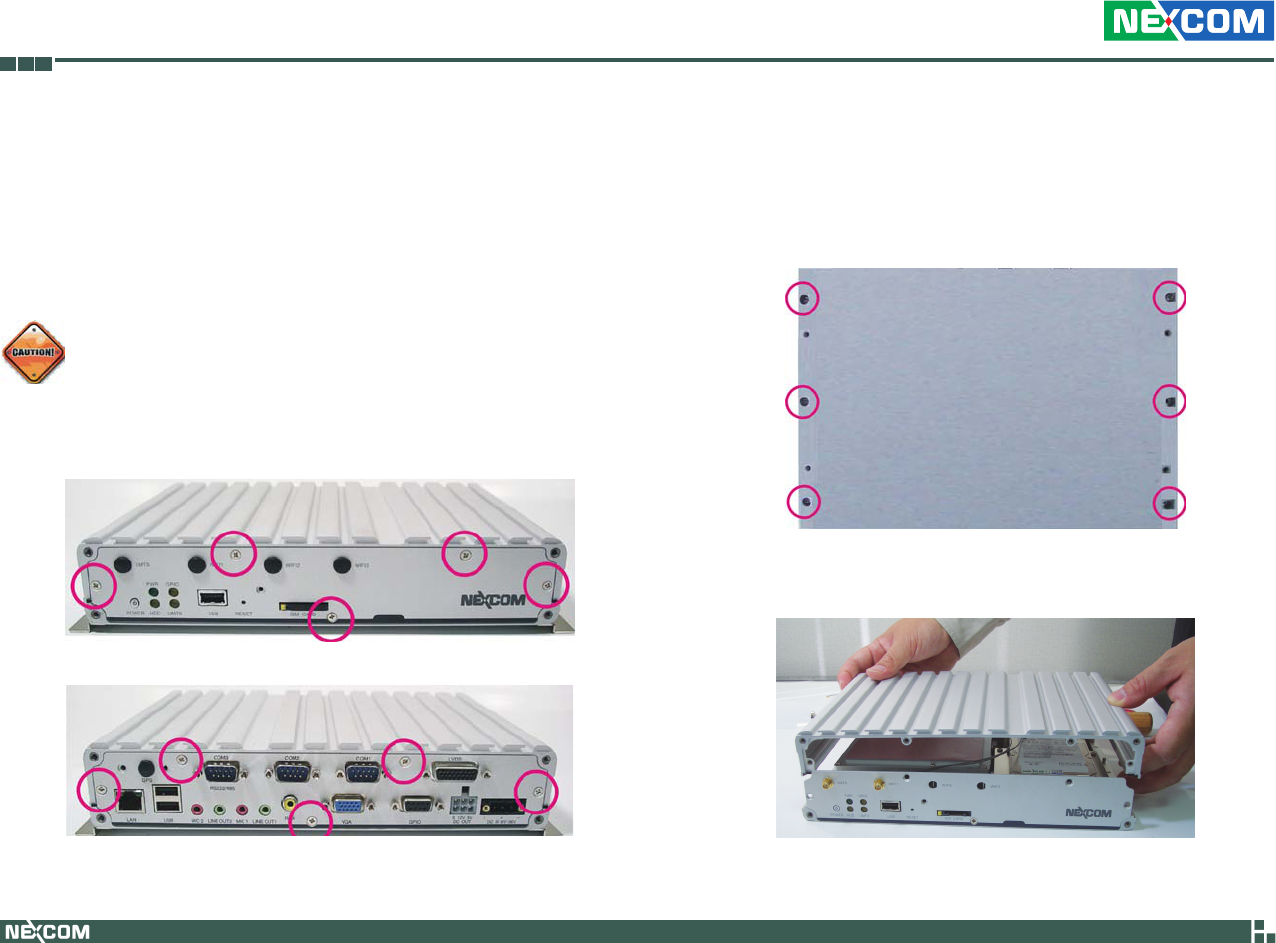
Removing the Chassis Cover
Front View
2. Lift the cover upward then remove it from the chassis.
Bottom View
Prior to removing the chassis cover, make sure the unit’s power is
off and disconnected from the power sources to prevent electric
shock or system damage.
1. The screws on the cover are used to secure the cover to the chassis.
Remove these screws and put them in a safe place for later use.
Rear View
Copyright © 2009 NEXCOM International Co., Ltd. All Rights Reserved. 39
Chapter 3: System Setup
VTC 6110 User Manual
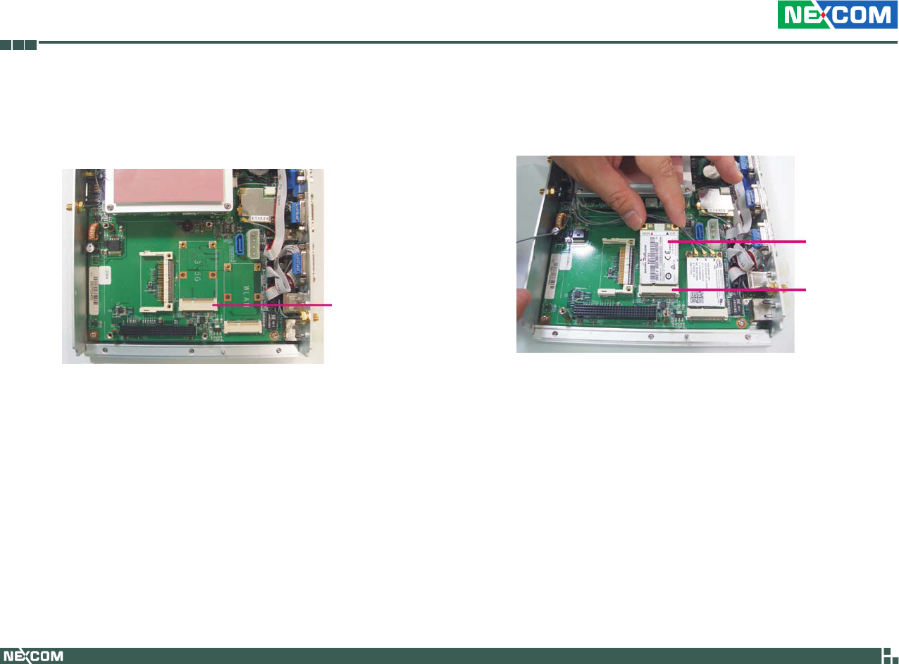
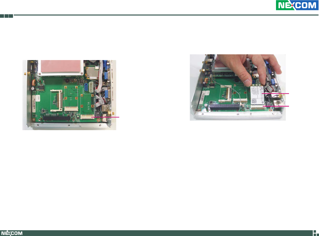
Installing a GPRS/UMTS/HSDPA Module
1. The Mini PCI Express slot shown below is used to install a 3.5G com-
munication module such as GPRS, UMTS or HSDPA module.
2. Insert the module into the Mini PCI Express slot at a 45 degrees angle
until the gold-plated connector on the edge of the module completely
disappears inside the slot.
Mini PCI
Express slot
GPRS/UMTS/
HSDPA module
Mini PCI
Express slot
Copyright © 2009 NEXCOM International Co., Ltd. All Rights Reserved. 40
Chapter 3: System Setup
VTC 6110 User Manual
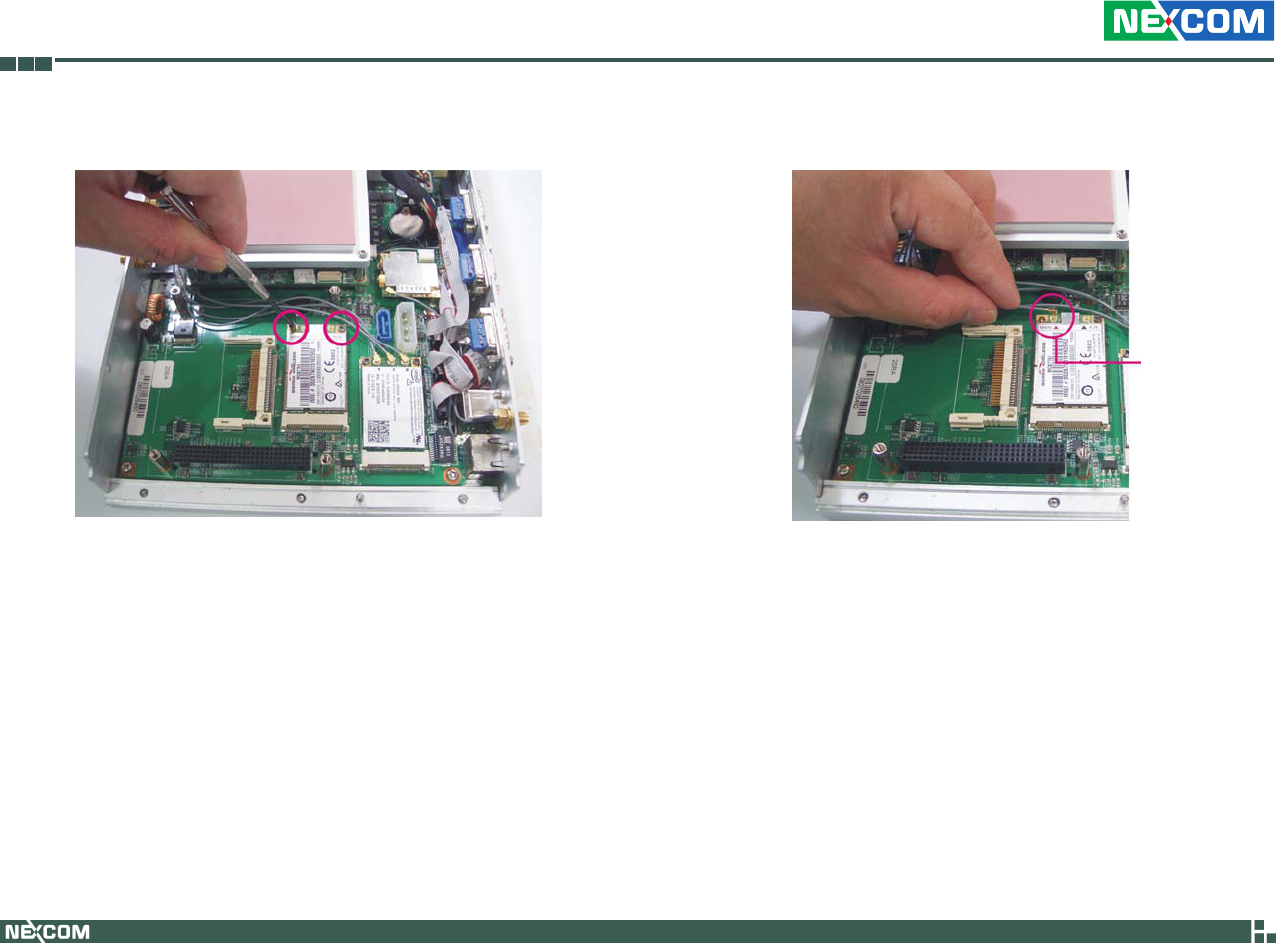
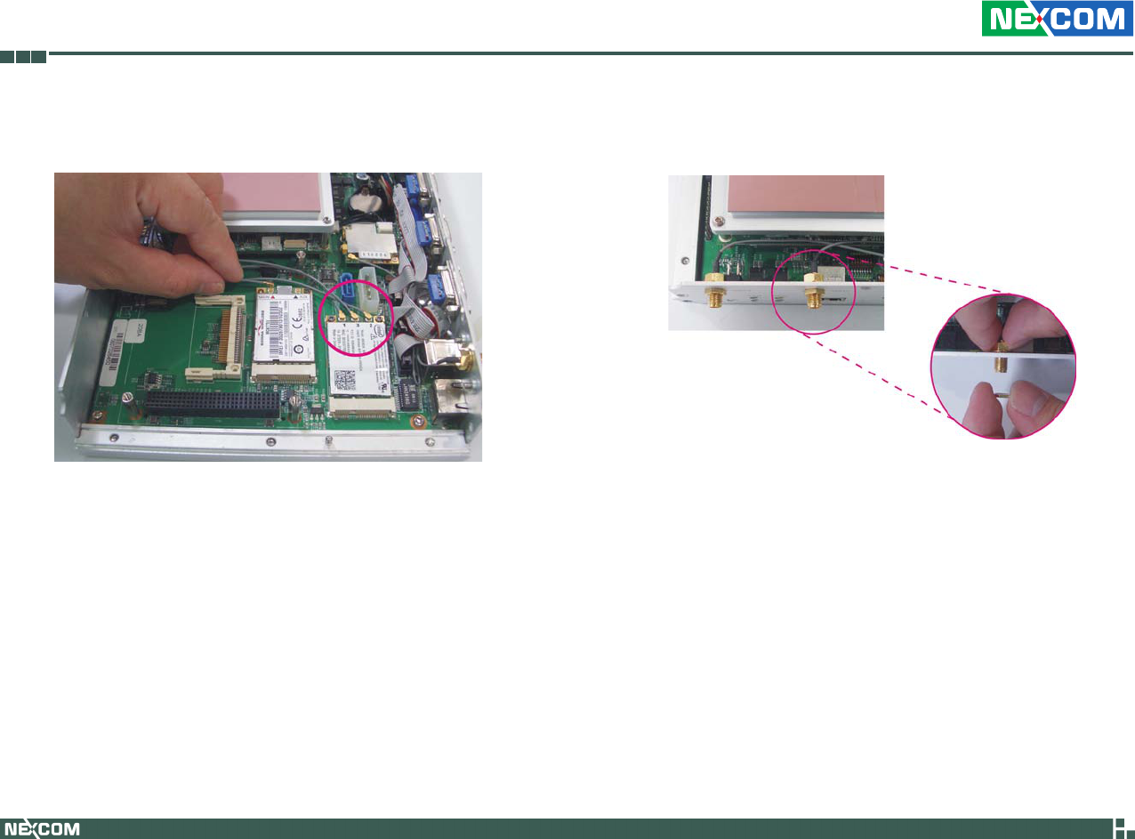
3. Push the module down then secure it with mounting screws. 4. Attach one end of the RF cable onto the module.
Attach RF cable
to the module
Copyright © 2009 NEXCOM International Co., Ltd. All Rights Reserved. 41
Chapter 3: System Setup
VTC 6110 User Manual
6. Mount the other end of the cable to the antenna mounting hole lo-
cated at the front panel of the chassis.
5. The photo below shows one end of the RF cable properly attached
onto the module.
RF cable mounted
at the front panel
Copyright © 2009 NEXCOM International Co., Ltd. All Rights Reserved. 42
Chapter 3: System Setup
VTC 6110 User Manual
Installing a Wireless LAN Module
1. The Mini PCI Express slot shown below is used to install a wireless LAN
module.
Mini PCI
Express slot
2. Insert the wireless LAN module into the Mini PCI Express slot at a 45
degrees angle until the gold-plated connector on the edge of the mod-
ule completely disappears inside the slot.
Wireless LAN
module
Mini PCI
Express slot

Copyright © 2009 NEXCOM International Co., Ltd. All Rights Reserved. 43
Chapter 3: System Setup
VTC 6110 User Manual
4. Attach one end of the RF cable onto the module.
Attach RF
cable to the
module
3. Push the module down then secure it with mounting screws.
Copyright © 2009 NEXCOM International Co., Ltd. All Rights Reserved. 44
Chapter 3: System Setup
VTC 6110 User Manual
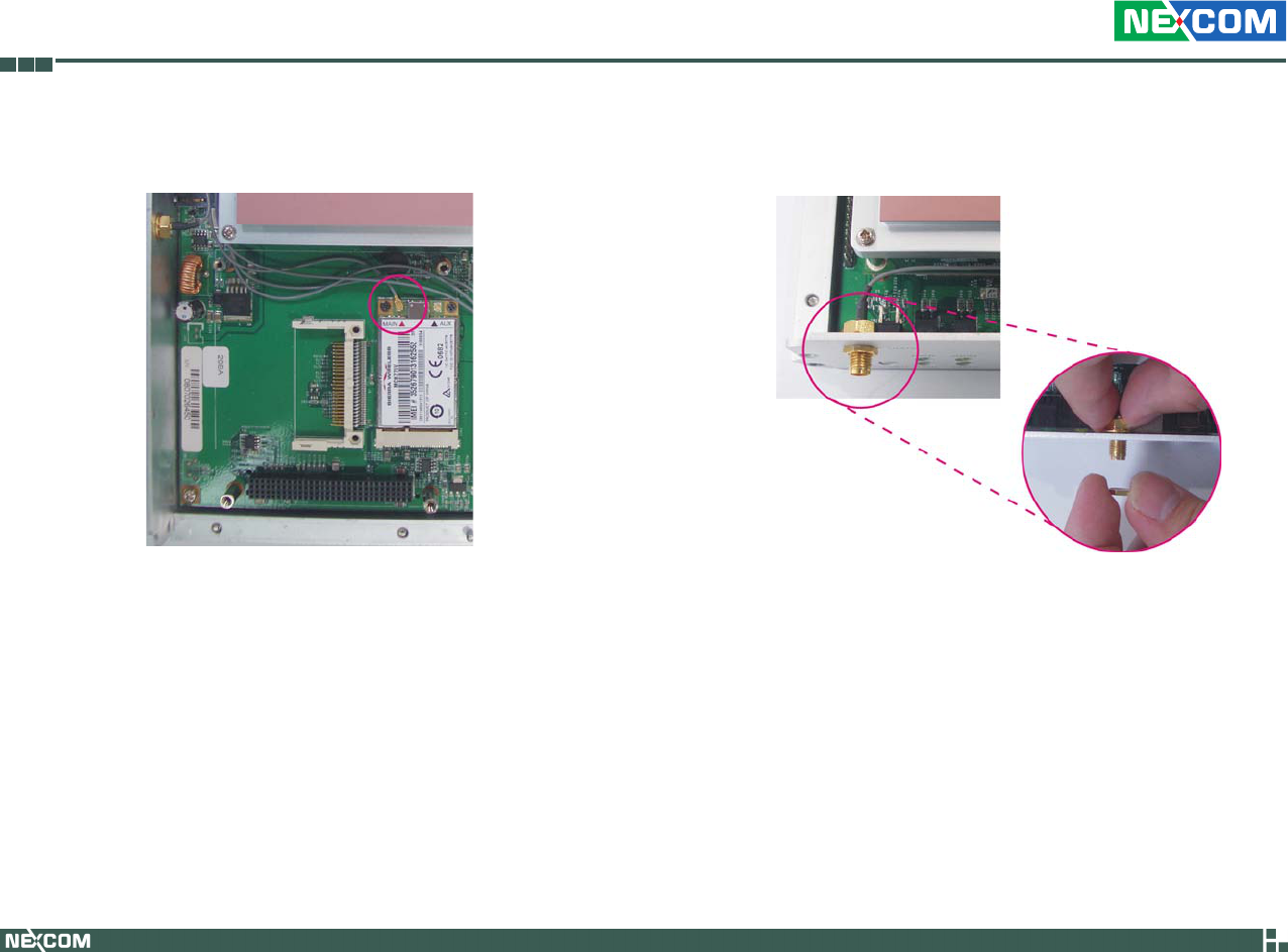
5. The photo below shows one end of the RF cable properly attached
onto the module.
6. Mount the other end of the cable to the antenna mounting hole lo-
cated at the front panel of the chassis.
RF cable mounted
at the front panel
Copyright © 2009 NEXCOM International Co., Ltd. All Rights Reserved. 45
Chapter 3: System Setup
VTC 6110 User Manual
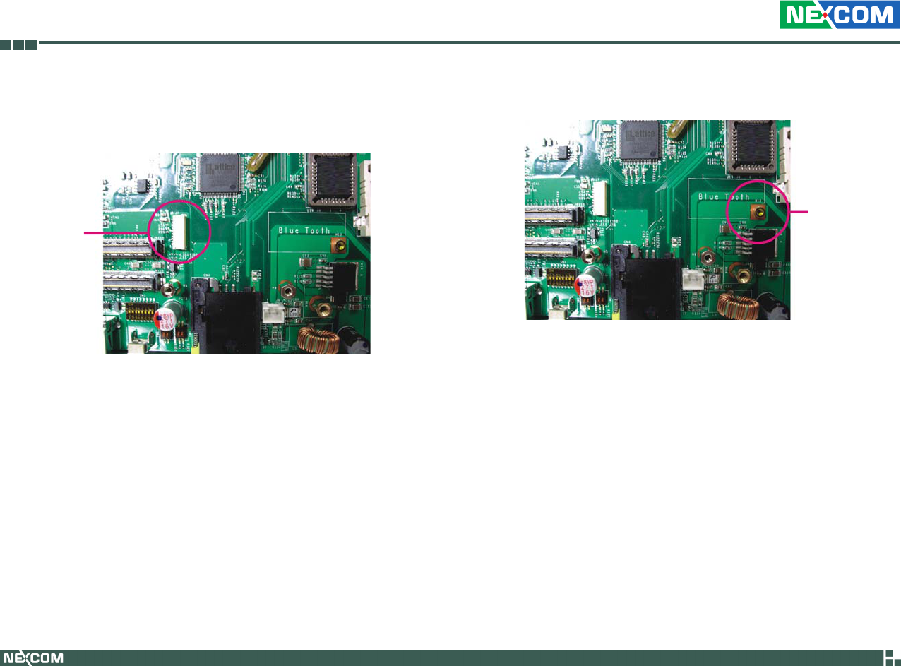
Installing a Bluetooth Module
1. The USB header shown below is used to install a Bluetooth module.
USB
header
2. Install the provided mounting stud as shown in the illustration below.
Mounting
stud
Copyright © 2009 NEXCOM International Co., Ltd. All Rights Reserved. 46
Chapter 3: System Setup
VTC 6110 User Manual
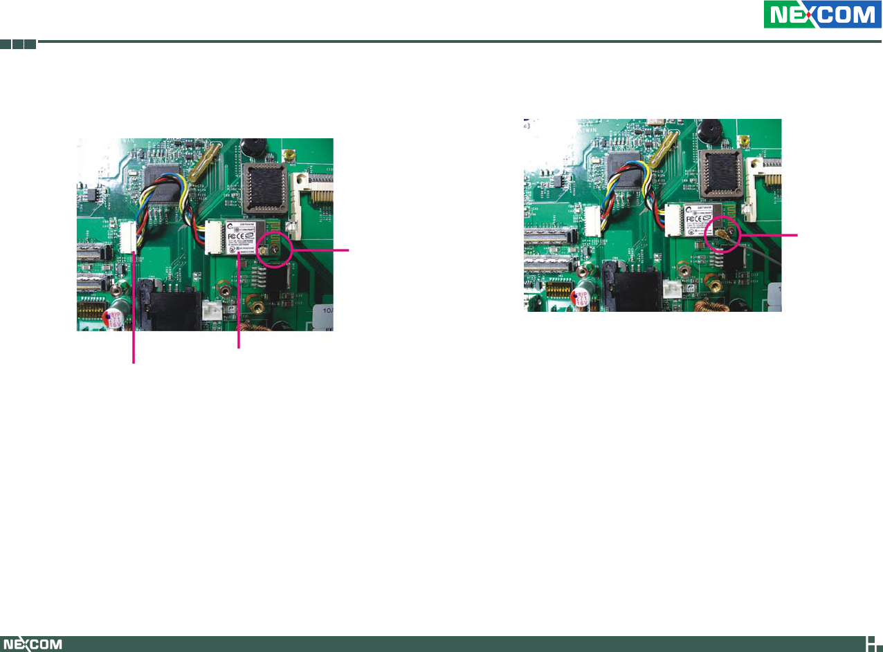
3. Insert the Bluetooth module’s cable connector into the USB header.
Push the module down then secure it with a mounting screw.
Bluetooth module
Cable connector
Mounting
screw
4. Attach one end of the RF cable onto the module.
Attach RF
cable to the
module
5. Mount the other end of the cable to the Bluetooth mounting hole
located at the front panel of the chassis.