Nokia Solutions and Networks T5BL1 Part 22 CDMA Cellular Base Station User Manual IHET5BL1 Part 1 of 3
Nokia Solutions and Networks Part 22 CDMA Cellular Base Station IHET5BL1 Part 1 of 3
Contents
- 1. IHET5BL1 User Manual Part 3 of 3
- 2. IHET5BL1 User Manual Part 1 of 3
- 3. IHET5BL1 User Manual Part 2 of 3
IHET5BL1 User Manual Part 1 of 3
SCt4812T BTS Optimization/ATP
System Software Release 2.16.0
800/1700/1900 MHz
CDMA
English
Mar 2001
68P09253A61–1 DRAFT
English
Mar 2001
68P09253A61–1
SCt4812T BTS Optimization/ATP
800/1700/1900 MHz
CDMA

SCt4812T BTS Optimization/ATP
System Software Release 2.16.0
800/1700/1900 MHz
CDMA
English
Mar 2001
68P09253A61–1DRAFT

Notice
While reasonable efforts have been made to assure the accuracy of this document, Motorola, Inc. assumes no liability resulting from any
inaccuracies or omissions in this document, or from use of the information obtained herein. The information in this document has been
carefully checked and is believed to be entirely reliable. However, no responsibility is assumed for inaccuracies or omissions. Motorola,
Inc. reserves the right to make changes to any products described herein and reserves the right to revise this document and to make
changes from time to time in content hereof with no obligation to notify any person of revisions or changes. Motorola, Inc. does not
assume any liability arising out of the application or use of any product, software, or circuit described herein; neither does it convey
license under its patent rights or the rights of others.
It is possible that this publication may contain references to, or information about Motorola products (machines and programs),
programming, or services that are not announced in your country. Such references or information must not be construed to mean
that Motorola intends to announce such Motorola products, programming, or services in your country.
Copyrights
This instruction manual, and the Motorola products described in this instruction manual may be, include or describe copyrighted
Motorola material, such as computer programs stored in semiconductor memories or other media. Laws in the United States and
other countries preserve for Motorola certain exclusive rights for copyrighted material, including the exclusive right to copy,
reproduce in any form, distribute and make derivative works of the copyrighted material. Accordingly, any copyrighted Motorola
material contained herein or in the Motorola products described in this instruction manual may not be copied, reproduced,
distributed, merged or modified in any manner without the express written permission of Motorola. Furthermore, the purchase of
Motorola products shall not be deemed to grant either directly or by implication, estoppel, or otherwise, any license under the
copyrights, patents or patent applications of Motorola, as arises by operation of law in the sale of a product.
Usage and Disclosure Restrictions
License Agreement
The software described in this document is the property of Motorola, Inc. It is furnished by express license agreement only and may
be used only in accordance with the terms of such an agreement.
Copyrighted Materials
Software and documentation are copyrighted materials. Making unauthorized copies is prohibited by law. No part of the software or
documentation may be reproduced, transmitted, transcribed, stored in a retrieval system, or translated into any language or
computer language, in any form or by any means, without prior written permission of Motorola, Inc.
High Risk Activities
Components, units, or third–party products used in the product described herein are NOT fault–tolerant and are NOT designed,
manufactured, or intended for use as on–line control equipment in the following hazardous environments requiring fail–safe
controls: the operation of Nuclear Facilities, Aircraft Navigation or Aircraft Communication Systems, Air Traffic Control, Life
Support, or Weapons Systems (“High Risk Activities”). Motorola and its supplier(s) specifically disclaim any expressed or implied
warranty of fitness for such High Risk Activities.
Trademarks
and Motorola are registered trademarks of Motorola, Inc.
Product and service names profiled herein are trademarks of Motorola, Inc. Other manufacturers’ products or services profiled
herein may be referred to by trademarks of their respective companies.
Copyright
Copyright 2001 Motorola, Inc.
All Rights Reserved
Printed on
Recyclable Paper
REV010598
SPECIFICATIONS SUBJECT TO CHANGE WITHOUT NOTICE

Mar 2001 i
SCt4812T CDMA BTS Optimization/ATP DRAFT
Table of Contents
SCt4812T CDMA BTS Optimization/ATP
CDMA 800/1700/1900 MHz
List of Figures iv. . . . . . . . . . . . . . . . . . . . . . . . . . . . . . . . . . . . . . . . . . . . . . . . . . .
List of Tables vi. . . . . . . . . . . . . . . . . . . . . . . . . . . . . . . . . . . . . . . . . . . . . . . . . . .
Product Information x. . . . . . . . . . . . . . . . . . . . . . . . . . . . . . . . . . . . . . . . . . . . . .
FCC Part 15 xi. . . . . . . . . . . . . . . . . . . . . . . . . . . . . . . . . . . . . . . . . . . . . . . . . . . .
FCC Part 68 xiii. . . . . . . . . . . . . . . . . . . . . . . . . . . . . . . . . . . . . . . . . . . . . . . . . . . .
General Safety xvii. . . . . . . . . . . . . . . . . . . . . . . . . . . . . . . . . . . . . . . . . . . . . . . . . . .
Revision History xix. . . . . . . . . . . . . . . . . . . . . . . . . . . . . . . . . . . . . . . . . . . . . . . . .
Patent Notification xx. . . . . . . . . . . . . . . . . . . . . . . . . . . . . . . . . . . . . . . . . . . . . . .
Chapter 1: Introduction
Optimization Manual: Scope and Layout 1-1. . . . . . . . . . . . . . . . . . . . . . . . . . . . . .
Purpose of the Optimization 1-4. . . . . . . . . . . . . . . . . . . . . . . . . . . . . . . . . . . . . . . .
Required Test Equipment 1-6. . . . . . . . . . . . . . . . . . . . . . . . . . . . . . . . . . . . . . . . . .
Required Documentation 1-12. . . . . . . . . . . . . . . . . . . . . . . . . . . . . . . . . . . . . . . . . .
BTS Equipment Identification 1-13. . . . . . . . . . . . . . . . . . . . . . . . . . . . . . . . . . . . . .
Frame Module Location & Identification 1-21. . . . . . . . . . . . . . . . . . . . . . . . . . . . . .
Chapter 2: Preliminary Operations
Preliminary Operations: Overview 2-1. . . . . . . . . . . . . . . . . . . . . . . . . . . . . . . . . . .
Pre–Power–up Tests 2-4. . . . . . . . . . . . . . . . . . . . . . . . . . . . . . . . . . . . . . . . . . . . . .
Initial Power–up Tests 2-12. . . . . . . . . . . . . . . . . . . . . . . . . . . . . . . . . . . . . . . . . . . .
Chapter 3: Optimization/Calibration
Optimization/Calibration – Introduction 3-1. . . . . . . . . . . . . . . . . . . . . . . . . . . . . .
Isolate Span Lines/Connect LMF 3-4. . . . . . . . . . . . . . . . . . . . . . . . . . . . . . . . . . . .
Preparing the LMF 3-7. . . . . . . . . . . . . . . . . . . . . . . . . . . . . . . . . . . . . . . . . . . . . . .
Using CDMA LMF 3-18. . . . . . . . . . . . . . . . . . . . . . . . . . . . . . . . . . . . . . . . . . . . . .
Download the BTS 3-25. . . . . . . . . . . . . . . . . . . . . . . . . . . . . . . . . . . . . . . . . . . . . . .
CSM System Time/GPS and LFR/HSO Verification 3-32. . . . . . . . . . . . . . . . . . . . .
Test Equipment Set–up 3-43. . . . . . . . . . . . . . . . . . . . . . . . . . . . . . . . . . . . . . . . . . . .
Test Set Calibration 3-53. . . . . . . . . . . . . . . . . . . . . . . . . . . . . . . . . . . . . . . . . . . . . . .
. . . continued on next page

Table of Contents – continued
DRAFT
SCt4812T CDMA BTS Optimization/ATP Mar 2001
ii
Bay Level Offset Calibration 3-63. . . . . . . . . . . . . . . . . . . . . . . . . . . . . . . . . . . . . . .
RFDS Setup and Calibration 3-75. . . . . . . . . . . . . . . . . . . . . . . . . . . . . . . . . . . . . . .
BTS Redundancy/Alarm Testing 3-85. . . . . . . . . . . . . . . . . . . . . . . . . . . . . . . . . . . .
BTS Alarms Testing 3-97. . . . . . . . . . . . . . . . . . . . . . . . . . . . . . . . . . . . . . . . . . . . . .
Chapter 4: Automated Acceptance Test Procedure (ATP)
Automated Acceptance Test Procedures – All–inclusive TX & RX 4-1. . . . . . . . .
TX Output Acceptance Tests: Introduction 4-5. . . . . . . . . . . . . . . . . . . . . . . . . . . .
TX Spectral Purity Transmit Mask Acceptance Test 4-6. . . . . . . . . . . . . . . . . . . . .
TX Waveform Quality (rho) Acceptance Test 4-8. . . . . . . . . . . . . . . . . . . . . . . . . .
TX Pilot Time Offset Acceptance Test 4-9. . . . . . . . . . . . . . . . . . . . . . . . . . . . . . . .
TX Code Domain Power/Noise Floor Acceptance Test 4-10. . . . . . . . . . . . . . . . . . .
RX Frame Error Rate (FER) Acceptance Test 4-12. . . . . . . . . . . . . . . . . . . . . . . . . .
Generate an ATP Report 4-13. . . . . . . . . . . . . . . . . . . . . . . . . . . . . . . . . . . . . . . . . . .
Chapter 5: Prepare to Leave the Site
Prepare to Leave the Site 5-1. . . . . . . . . . . . . . . . . . . . . . . . . . . . . . . . . . . . . . . . . .
Chapter 6: Basic Troubleshooting
Basic Troubleshooting Overview 6-1. . . . . . . . . . . . . . . . . . . . . . . . . . . . . . . . . . . .
Troubleshooting: Installation 6-2. . . . . . . . . . . . . . . . . . . . . . . . . . . . . . . . . . . . . . .
Troubleshooting: Download 6-4. . . . . . . . . . . . . . . . . . . . . . . . . . . . . . . . . . . . . . . .
Troubleshooting: Calibration 6-6. . . . . . . . . . . . . . . . . . . . . . . . . . . . . . . . . . . . . . .
Troubleshooting: Transmit ATP 6-8. . . . . . . . . . . . . . . . . . . . . . . . . . . . . . . . . . . . .
Troubleshooting: Receive ATP 6-10. . . . . . . . . . . . . . . . . . . . . . . . . . . . . . . . . . . . . .
Troubleshooting: CSM Checklist 6-11. . . . . . . . . . . . . . . . . . . . . . . . . . . . . . . . . . . .
C–CCP Backplane Troubleshooting 6-13. . . . . . . . . . . . . . . . . . . . . . . . . . . . . . . . . .
Module Front Panel LED Indicators and Connectors 6-20. . . . . . . . . . . . . . . . . . . . .
Basic Troubleshooting – Span Control Link 6-27. . . . . . . . . . . . . . . . . . . . . . . . . . .
Appendix A: Data Sheets
Optimization (Pre–ATP) Data Sheets A-1. . . . . . . . . . . . . . . . . . . . . . . . . . . . . . . . .
Site Serial Number Check List A-18. . . . . . . . . . . . . . . . . . . . . . . . . . . . . . . . . . . . . .
Appendix B: PN Offset/I & Q Offset Register Programming Information
PN Offset Programming Information B-1. . . . . . . . . . . . . . . . . . . . . . . . . . . . . . . . .
Appendix C: FRU Optimization/ATP Test Matrix
FRU Optimization/ATP Test Matrix C-1. . . . . . . . . . . . . . . . . . . . . . . . . . . . . . . . . .
Appendix D: BBX Gain Set Point vs. BTS Output Considerations
BBX Gain Set Point vs. BTS Output Considerations D-1. . . . . . . . . . . . . . . . . . . .
. . . continued on next page

Table of Contents – continued
Mar 2001 iii
SCt4812T CDMA BTS Optimization/ATP DRAFT
Appendix E: CDMA Operating Frequency Information
CDMA Operating Frequency Programming Information – North
American PCS Bands E-1. . . . . . . . . . . . . . . . . . . . . . . . . . . . . . . . . . . . . . . . . . . . .
CDMA Operating Frequency Programming Information – Korean Bands E-6. . . .
Appendix F: PCS Interface Setup for Manual Testing
Test Equipment Setup F-1. . . . . . . . . . . . . . . . . . . . . . . . . . . . . . . . . . . . . . . . . . . . .
Appendix G: VSWR
Transmit & Receive Antenna VSWR G-1. . . . . . . . . . . . . . . . . . . . . . . . . . . . . . . . .
Appendix H: Download ROM Code
Download ROM Code H-1. . . . . . . . . . . . . . . . . . . . . . . . . . . . . . . . . . . . . . . . . . . .
Appendix I: In–Service Calibration
Introduction I-1. . . . . . . . . . . . . . . . . . . . . . . . . . . . . . . . . . . . . . . . . . . . . . . . . . . . .
Power Delta Calibration I-2. . . . . . . . . . . . . . . . . . . . . . . . . . . . . . . . . . . . . . . . . . .
In–Service Calibration I-10. . . . . . . . . . . . . . . . . . . . . . . . . . . . . . . . . . . . . . . . . . . .
Index Index-1. . . . . . . . . . . . . . . . . . . . . . . . . . . . . . . . . . . . . . . . . . . . . . . . . . . . . . . . . . . . . . . . . . . . . . . . . . . . . .

DRAFT
SCt4812T CDMA BTS Optimization/ATP Mar 2001
iv
List of Figures
SCt4812T CDMA BTS Optimization/ATP
CDMA 800/1700/1900 MHz
Figure 1-1: Null Modem Cable Detail 1-8. . . . . . . . . . . . . . . . . . . . . . . . . . . . . . . .
Figure 1-2: +27 V SC 4812T BTS Starter Frame 1-15. . . . . . . . . . . . . . . . . . . . . . .
Figure 1-3: –48 V SC 4812T BTS Starter Frame 1-16. . . . . . . . . . . . . . . . . . . . . . . .
Figure 1-4: +27 V SC 4812T BTS Expansion Frame 1-17. . . . . . . . . . . . . . . . . . . .
Figure 1-5: –48 V SC 4812T BTS Expansion Frame 1-18. . . . . . . . . . . . . . . . . . . .
Figure 1-6: +27 V SC 4812T Starter Frame I/O Plate 1-21. . . . . . . . . . . . . . . . . . . .
Figure 1-7: –48 V SC 4812T Starter Frame I/O Plate 1-22. . . . . . . . . . . . . . . . . . . .
Figure 1-8: +27 V SC 4812T Expansion Frame I/O Plate 1-23. . . . . . . . . . . . . . . . .
Figure 1-9: –48 V SC 4812T Expansion Frame I/O Plate 1-24. . . . . . . . . . . . . . . . .
Figure 1-10: SC 4812T C–CCP Shelf 1-25. . . . . . . . . . . . . . . . . . . . . . . . . . . . . . . .
Figure 1-11: +27 V SC 4812T LPA Configuration – 4 Carrier with
2:1 Combiners 1-26. . . . . . . . . . . . . . . . . . . . . . . . . . . . . . . . . . . . . . . . . . . . . . . . . . .
Figure 1-12: –48 V SC 4812T LPA Configuration – 4 Carrier, 3–Sector
with 2:1 Combiners 1-27. . . . . . . . . . . . . . . . . . . . . . . . . . . . . . . . . . . . . . . . . . . . . .
Figure 1-13: +27 V SC4812T LPA Configuration with Combiners/Filters 1-30. . . .
Figure 1-14: –48 V SC4812T LPA Configuration with Combiners/Filters 1-31. . . .
Figure 1-15: –48 V BTS Power Conversion Shelf 1-32. . . . . . . . . . . . . . . . . . . . . . .
Figure 1-16: CDMA (COBRA) RFDS Layout 1-33. . . . . . . . . . . . . . . . . . . . . . . . .
Figure 2-1: Switch Card 2-2. . . . . . . . . . . . . . . . . . . . . . . . . . . . . . . . . . . . . . . . . . .
Figure 2-2: Backplane DIP Switch Settings – SC 4812T 2-3. . . . . . . . . . . . . . . . .
Figure 2-3: +27 V BTS DC Distribution Pre-test 2-7. . . . . . . . . . . . . . . . . . . . . . . .
Figure 2-4: +27 V SC 4812T BTS Starter Frame 2-8. . . . . . . . . . . . . . . . . . . . . . .
Figure 2-5: –48 V BTS DC Distribution Pre-test 2-9. . . . . . . . . . . . . . . . . . . . . . . .
Figure 2-6: –48 V SC 4812T BTS Starter Frame 2-10. . . . . . . . . . . . . . . . . . . . . . . .
Figure 2-7: DC Distribution Pre-test (COBRA RFDS Detail) 2-11. . . . . . . . . . . . . .
Figure 3-1: Span I/O Board T1 Span Isolation 3-5. . . . . . . . . . . . . . . . . . . . . . . . . .
Figure 3-2: LMF Connection Detail 3-6. . . . . . . . . . . . . . . . . . . . . . . . . . . . . . . . . .
Figure 3-3: LMF Folder Structure 3-13. . . . . . . . . . . . . . . . . . . . . . . . . . . . . . . . . . .
Figure 3-4: BTS LAN Interconnect Diagram 3-14. . . . . . . . . . . . . . . . . . . . . . . . . . .
Figure 3-5: +27 V SC 4812T Starter Frame I/O Plate 3-16. . . . . . . . . . . . . . . . . . . .
. . . continued on next page

List of Figures – continued
Mar 2001 v
SCt4812T CDMA BTS Optimization/ATP DRAFT
Figure 3-6: –48 V SC 4812T Starter Frame I/O Plate 3-17. . . . . . . . . . . . . . . . . . . .
Figure 3-7: CDMA LMF Computer Common MMI Connections 3-24. . . . . . . . . . .
Figure 3-8: Null Modem Cable Detail 3-34. . . . . . . . . . . . . . . . . . . . . . . . . . . . . . . .
Figure 3-9: CSM MMI terminal connection 3-35. . . . . . . . . . . . . . . . . . . . . . . . . . . .
Figure 3-10: Cable Calibration Test Setup 3-46. . . . . . . . . . . . . . . . . . . . . . . . . . . . .
Figure 3-11: TX Calibration Test Setup (CyberTest, HP 8935,
and Advantest) 3-47. . . . . . . . . . . . . . . . . . . . . . . . . . . . . . . . . . . . . . . . . . . . . . . . . .
Figure 3-12: TX Calibration Test Setup HP 8921A W/PCS for 1.7/1.9 GHz 3-48. .
Figure 3-13: Optimization/ATP Test Setup Calibration (CyberTest,
HP 8935 and Advantest) 3-49. . . . . . . . . . . . . . . . . . . . . . . . . . . . . . . . . . . . . . . . . . .
Figure 3-14: Optimization/ATP Test Setup HP 8921A 3-50. . . . . . . . . . . . . . . . . . .
Figure 3-15: Typical TX ATP Setup with Directional Coupler (shown
with and without RFDS) 3-51. . . . . . . . . . . . . . . . . . . . . . . . . . . . . . . . . . . . . . . . . . .
Figure 3-16: Typical RX ATP Setup with Directional Coupler (shown
with or without RFDS) 3-52. . . . . . . . . . . . . . . . . . . . . . . . . . . . . . . . . . . . . . . . . . . .
Figure 3-17: Calibrating Test Equipment Setup for TX BLO and TX
ATP Tests (using Signal Generator and Spectrum Analyzer) 3-59. . . . . . . . . . . . . . .
Figure 3-18: Calibrating Test Equipment Setup for RX ATP Test (using
Signal Generator and Spectrum Analyzer) 3-60. . . . . . . . . . . . . . . . . . . . . . . . . . . . .
Figure 3-19: SC 4812T C–CCP Shelf 3-88. . . . . . . . . . . . . . . . . . . . . . . . . . . . . . . .
Figure 3-20: –48 V BTS Power Conversion Shelf 3-88. . . . . . . . . . . . . . . . . . . . . . .
Figure 3-21: +27 V BTS C-CCP Fan Modules 3-90. . . . . . . . . . . . . . . . . . . . . . . . .
Figure 3-22: –48 V BTS C-CCP and Power Conversion Shelf Fan Modules 3-90. .
Figure 3-23: +27 V SC 4812T Starter Frame I/O Plate 3-94. . . . . . . . . . . . . . . . . . .
Figure 3-24: Alarm Connector Location and Connector Pin Numbering 3-98. . . . .
Figure 3-25: AMR Connector Pin Numbering 3-99. . . . . . . . . . . . . . . . . . . . . . . . . .
Figure 4-1: TX Mask Verification Spectrum Analyzer Display 4-7. . . . . . . . . . . . .
Figure 4-2: Code Domain Power and Noise Floor Levels 4-11. . . . . . . . . . . . . . . . .
Figure 5-1: MGLI2/SGLI2 MMI Port Connection 5-4. . . . . . . . . . . . . . . . . . . . . . .
Figure 5-2: Site and Span I/O Boards T1 Span Connections 5-8. . . . . . . . . . . . . . .
Figure 6-1: CSM Front Panel Indicators & Monitor Ports 6-21. . . . . . . . . . . . . . . . .
Figure 6-2: GLI2 Front Panel 6-24. . . . . . . . . . . . . . . . . . . . . . . . . . . . . . . . . . . . . . .
Figure 6-3: MCC24/8E Front Panel 6-26. . . . . . . . . . . . . . . . . . . . . . . . . . . . . . . . . .
Figure E-1: North American PCS 1900 MHz Frequency
Spectrum (CDMA Allocation) E-1. . . . . . . . . . . . . . . . . . . . . . . . . . . . . . . . . . . . . .
Figure E-2: North American Cellular Telephone System Frequency
Spectrum (CDMA Allocation) E-4. . . . . . . . . . . . . . . . . . . . . . . . . . . . . . . . . . . . . .
Figure E-3: 1700 MHz PCS Frequency Spectrum (CDMA Allocation) E-6. . . . . .
Figure F-1: Calibrating Test Setup Components F-6. . . . . . . . . . . . . . . . . . . . . . . .
Figure F-2: Cable Calibration using Advantest R3465 F-10. . . . . . . . . . . . . . . . . . .
. . . continued on next page

List of Figures – continued
DRAFT
SCt4812T CDMA BTS Optimization/ATP Mar 2001
vi
Figure G-1: Manual VSWR Test Setup Using HP8921 Test Set
(1700/1900 MHz) G-3. . . . . . . . . . . . . . . . . . . . . . . . . . . . . . . . . . . . . . . . . . . . . . . .
Figure G-2: Manual VSWR Test Setup Using HP8921 Test Set (800 MHz) G-4. .
Figure G-3: Manual VSWR Test Setup Using Advantest R3465 G-6. . . . . . . . . . .
Figure I-1: Delta Calibration Setup – HP8921A to HP437B I-4. . . . . . . . . . . . . . .
Figure I-2: Delta Calibration Setup – HP8921A to HP8921A I-4. . . . . . . . . . . . . .
Figure I-3: Delta Calibration Setup – R3561L to HP437B I-6. . . . . . . . . . . . . . . .
Figure I-4: Delta Calibration Setup – R3561L to R3465 I-7. . . . . . . . . . . . . . . . . .
Figure I-5: Delta Calibration Setup – HP8935 to HP437B I-8. . . . . . . . . . . . . . . .
Figure I-6: Delta Calibration Setup – HP8935 to HP8935 I-9. . . . . . . . . . . . . . . . .
Figure I-7: Optimization/ATP Test Setup Using Directional Coupler I-11. . . . . . . .
Figure I-8: Optimization/ATP Test Setup Using RFDS I-12. . . . . . . . . . . . . . . . . . .

Mar 2001 vii
SCt4812T CDMA BTS Optimization/ATP DRAFT
List of Tables
SCt4812T CDMA BTS Optimization/ATP
CDMA 800/1700/1900 MHz
Table 1-1: C–CCP Shelf/Cage Card/Module Device ID
Numbers (Top Shelf) 1-14. . . . . . . . . . . . . . . . . . . . . . . . . . . . . . . . . . . . . . . . . . . . .
Table 1-2: C–CCP Shelf/Cage Card/Module Device ID
Numbers (Bottom Shelf) 1-14. . . . . . . . . . . . . . . . . . . . . . . . . . . . . . . . . . . . . . . . . . .
Table 1-3: BTS Sector Configuration 1-28. . . . . . . . . . . . . . . . . . . . . . . . . . . . . . . . .
Table 1-4: Sector Configurations 1-29. . . . . . . . . . . . . . . . . . . . . . . . . . . . . . . . . . . .
Table 2-1: Initial Installation of Boards/Modules 2-2. . . . . . . . . . . . . . . . . . . . . . . .
Table 2-2: DC Power Pre–test (BTS Frame) 2-5. . . . . . . . . . . . . . . . . . . . . . . . . . .
Table 2-3: DC Power Pre-test (RFDS) 2-11. . . . . . . . . . . . . . . . . . . . . . . . . . . . . . . .
Table 2-4: DC Input Power Cable Guidelines 2-13. . . . . . . . . . . . . . . . . . . . . . . . . .
Table 2-5: Common Power Supply Verification 2-13. . . . . . . . . . . . . . . . . . . . . . . . .
Table 2-6: Initial Power-up (RFDS) 2-14. . . . . . . . . . . . . . . . . . . . . . . . . . . . . . . . . .
Table 2-7: Initial Power–up (BTS) 2-14. . . . . . . . . . . . . . . . . . . . . . . . . . . . . . . . . . .
Table 3-1: T1/E1 Span Isolation 3-4. . . . . . . . . . . . . . . . . . . . . . . . . . . . . . . . . . . . .
Table 3-2: LMF to BTS Connection 3-5. . . . . . . . . . . . . . . . . . . . . . . . . . . . . . . . . .
Table 3-3: LMF Operating System Installation 3-7. . . . . . . . . . . . . . . . . . . . . . . . .
Table 3-4: Copying CBSC CDF Files to the LMF 3-9. . . . . . . . . . . . . . . . . . . . . . .
Table 3-5: Creating a Named Hyperlink Connection for MMI Connection 3-11. . . .
Table 3-6: Pinging the Processors 3-15. . . . . . . . . . . . . . . . . . . . . . . . . . . . . . . . . . . .
Table 3-7: BTS GUI Login Procedure 3-20. . . . . . . . . . . . . . . . . . . . . . . . . . . . . . . .
Table 3-8: BTS CLI Login Procedure 3-22. . . . . . . . . . . . . . . . . . . . . . . . . . . . . . . .
Table 3-9: BTS GUI Logout Procedure 3-22. . . . . . . . . . . . . . . . . . . . . . . . . . . . . . .
Table 3-10: BTS CLI Logout Procedure 3-23. . . . . . . . . . . . . . . . . . . . . . . . . . . . . .
Table 3-11: Establishing MMI Communications 3-24. . . . . . . . . . . . . . . . . . . . . . . .
Table 3-12: Download and Enable MGLI2 3-27. . . . . . . . . . . . . . . . . . . . . . . . . . . .
Table 3-13: Download Code and Data to Non–MGLI Devices 3-28. . . . . . . . . . . . .
Table 3-14: Select CSM Clock Source 3-29. . . . . . . . . . . . . . . . . . . . . . . . . . . . . . . .
Table 3-15: Enable CSMs 3-30. . . . . . . . . . . . . . . . . . . . . . . . . . . . . . . . . . . . . . . . . .
Table 3-16: Enable MCCs 3-31. . . . . . . . . . . . . . . . . . . . . . . . . . . . . . . . . . . . . . . . .
Table 3-17: Enable Redundant GLIs 3-31. . . . . . . . . . . . . . . . . . . . . . . . . . . . . . . . .
. . . continued on next page

List of Tables – continued
DRAFT
SCt4812T CDMA BTS Optimization/ATP Mar 2001
viii
Table 3-18: Test Equipment Setup (GPS & LFR/HSO Verification) 3-34. . . . . . . . .
Table 3-19: GPS Initialization/Verification 3-36. . . . . . . . . . . . . . . . . . . . . . . . . . . .
Table 3-20: LFR Initialization/Verification 3-40. . . . . . . . . . . . . . . . . . . . . . . . . . . .
Table 3-21: HSO Initialization/Verification 3-42. . . . . . . . . . . . . . . . . . . . . . . . . . . .
Table 3-22: Test Equipment Setup 3-44. . . . . . . . . . . . . . . . . . . . . . . . . . . . . . . . . . .
Table 3-23: Selecting Test Equipment Manually in a Serial Connection Tab 3-54. .
Table 3-24: Selecting Test Equipment Using Auto-Detect 3-55. . . . . . . . . . . . . . . . .
Table 3-25: Test Equipment Calibration 3-56. . . . . . . . . . . . . . . . . . . . . . . . . . . . . . .
Table 3-26: Cable Calibration 3-57. . . . . . . . . . . . . . . . . . . . . . . . . . . . . . . . . . . . . . .
Table 3-27: Calibrating TX Cables Using Signal Generator and
Spectrum Analyzer 3-58. . . . . . . . . . . . . . . . . . . . . . . . . . . . . . . . . . . . . . . . . . . . . . .
Table 3-28: Calibrating RX Cables Using a Signal Generator and
Spectrum Analyzer 3-59. . . . . . . . . . . . . . . . . . . . . . . . . . . . . . . . . . . . . . . . . . . . . . .
Table 3-29: Setting Cable Loss Values 3-61. . . . . . . . . . . . . . . . . . . . . . . . . . . . . . . .
Table 3-30: Setting TX Coupler Loss Value 3-62. . . . . . . . . . . . . . . . . . . . . . . . . . . .
Table 3-31: BLO BTS.cal File Array Assignments 3-65. . . . . . . . . . . . . . . . . . . . . .
Table 3-32: BTS.cal File Array (Per Sector) 3-66. . . . . . . . . . . . . . . . . . . . . . . . . . .
Table 3-33: Test Equipment Setup (RF Path Calibration) 3-67. . . . . . . . . . . . . . . . .
Table 3-34: BTS TX Path Calibration 3-69. . . . . . . . . . . . . . . . . . . . . . . . . . . . . . . .
Table 3-35: Download BLO 3-70. . . . . . . . . . . . . . . . . . . . . . . . . . . . . . . . . . . . . . . .
Table 3-36: BTS TX Path Audit 3-72. . . . . . . . . . . . . . . . . . . . . . . . . . . . . . . . . . . . .
Table 3-37: All Cal/Audit Test 3-73. . . . . . . . . . . . . . . . . . . . . . . . . . . . . . . . . . . . . .
Table 3-38: Create CAL File 3-74. . . . . . . . . . . . . . . . . . . . . . . . . . . . . . . . . . . . . . .
Table 3-39: RFDS Parameter Settings 3-77. . . . . . . . . . . . . . . . . . . . . . . . . . . . . . . .
Table 3-40: Definition of Parameters 3-78. . . . . . . . . . . . . . . . . . . . . . . . . . . . . . . . .
Table 3-41: Valid NAM Field Ranges 3-79. . . . . . . . . . . . . . . . . . . . . . . . . . . . . . . .
Table 3-42: Set Antenna Map Data 3-80. . . . . . . . . . . . . . . . . . . . . . . . . . . . . . . . . . .
Table 3-43: Set RFDS Configuration Data 3-81. . . . . . . . . . . . . . . . . . . . . . . . . . . . .
Table 3-44: RFDS Calibration Procedure 3-82. . . . . . . . . . . . . . . . . . . . . . . . . . . . . .
Table 3-45: Program the TSU NAM 3-83. . . . . . . . . . . . . . . . . . . . . . . . . . . . . . . . .
Table 3-46: Test Equipment Setup for Redundancy/Alarm Tests 3-86. . . . . . . . . . . .
Table 3-47: Power Supply/Converter Redundancy (BTS Frame) 3-87. . . . . . . . . . .
Table 3-48: Miscellaneous Alarm Tests 3-89. . . . . . . . . . . . . . . . . . . . . . . . . . . . . . .
Table 3-49: BBX Redundancy Alarms 3-91. . . . . . . . . . . . . . . . . . . . . . . . . . . . . . . .
Table 3-50: CSM, GPS, & LFR/HSO, Redundancy/Alarm Tests 3-92. . . . . . . . . . .
Table 3-51: LPA Redundancy Test 3-95. . . . . . . . . . . . . . . . . . . . . . . . . . . . . . . . . . .
Table 3-52: MGLI/GLI Redundancy Test (with MM Connection Established) 3-96.
. . . continued on next page

List of Tables – continued
Mar 2001 ix
SCt4812T CDMA BTS Optimization/ATP DRAFT
Table 3-53: CDI Alarm Input Verification Using the Alarms Test Box 3-99. . . . . . .
Table 3-54: CDI Alarm Input Verification Without the Alarms Test Box 3-102. . . . .
Table 3-55: Pin and Signal Information for Alarm Connectors 3-103. . . . . . . . . . . . .
Table 4-1: ATP Test Procedure 4-3. . . . . . . . . . . . . . . . . . . . . . . . . . . . . . . . . . . . . .
Table 4-2: Generating an ATP Report 4-13. . . . . . . . . . . . . . . . . . . . . . . . . . . . . . . . .
Table 5-1: External Test Equipment Removal 5-1. . . . . . . . . . . . . . . . . . . . . . . . . .
Table 5-2: Enabling Devices 5-2. . . . . . . . . . . . . . . . . . . . . . . . . . . . . . . . . . . . . . . .
Table 5-3: BTS Span Parameter Configuration 5-3. . . . . . . . . . . . . . . . . . . . . . . . .
Table 5-4: Set BTS Span Parameter Configuration 5-4. . . . . . . . . . . . . . . . . . . . . .
Table 5-5: Backup CAL Data to a Diskette 5-6. . . . . . . . . . . . . . . . . . . . . . . . . . . .
Table 5-6: LMF Termination and Removal 5-7. . . . . . . . . . . . . . . . . . . . . . . . . . . .
Table 5-7: Procedures to Copy CAL Files from Diskette to the CBSC 5-7. . . . . . .
Table 5-8: T1/E1 Span/IFM Connections 5-8. . . . . . . . . . . . . . . . . . . . . . . . . . . . . .
Table 6-1: Login Failure Troubleshooting Procedures 6-2. . . . . . . . . . . . . . . . . . . .
Table 6-2: Troubleshooting a Power Meter Communication Failure 6-2. . . . . . . .
Table 6-3: Troubleshooting a Communications Analyzer
Communication Failure 6-3. . . . . . . . . . . . . . . . . . . . . . . . . . . . . . . . . . . . . . . . . . .
Table 6-4: Troubleshooting Code Download Failure 6-4. . . . . . . . . . . . . . . . . . . . .
Table 6-5: Troubleshooting Data Download Failure 6-4. . . . . . . . . . . . . . . . . . . . .
Table 6-6: Troubleshooting Device Enable (INS) Failure 6-5. . . . . . . . . . . . . . . . .
Table 6-7: Miscellaneous Failures 6-5. . . . . . . . . . . . . . . . . . . . . . . . . . . . . . . . . . .
Table 6-8: Troubleshooting BLO Calibration Failure 6-6. . . . . . . . . . . . . . . . . . . .
Table 6-9: Troubleshooting Calibration Audit Failure 6-7. . . . . . . . . . . . . . . . . . . .
Table 6-10: Troubleshooting TX Mask Measurement Failure 6-8. . . . . . . . . . . . . .
Table 6-11: Troubleshooting Rho and Pilot Time Offset
Measurement Failure 6-8. . . . . . . . . . . . . . . . . . . . . . . . . . . . . . . . . . . . . . . . . . . . .
Table 6-12: Troubleshooting Code Domain Power and Noise Floor
Measurement Failure 6-9. . . . . . . . . . . . . . . . . . . . . . . . . . . . . . . . . . . . . . . . . . . . .
Table 6-13: Troubleshooting Carrier Measurement Failure 6-9. . . . . . . . . . . . . . . .
Table 6-14: Troubleshooting Multi-FER Failure 6-10. . . . . . . . . . . . . . . . . . . . . . . .
Table 6-15: No GLI2 Control via LMF (all GLI2s) 6-15. . . . . . . . . . . . . . . . . . . . . .
Table 6-16: No GLI2 Control through Span Line Connection (Both GLI2s) 6-15. .
Table 6-17: MGLI2 Control Good – No Control over Co–located GLI2 6-15. . . . .
Table 6-18: MGLI2 Control Good – No Control over AMR 6-16. . . . . . . . . . . . . . .
Table 6-19: No BBX2 Control in the Shelf – No Control over
Co–located GLI2s 6-16. . . . . . . . . . . . . . . . . . . . . . . . . . . . . . . . . . . . . . . . . . . . . . . .
Table 6-20: MGLI2 Control Good – No (or Missing) Span Line Traffic 6-16. . . . . .
Table 6-21: No MCC24 Channel Elements 6-17. . . . . . . . . . . . . . . . . . . . . . . . . . . .
. . . continued on next page

List of Tables – continued
DRAFT
SCt4812T CDMA BTS Optimization/ATP Mar 2001
x
Table 6-22: No DC Input Voltage to Power Supply Module 6-18. . . . . . . . . . . . . . .
Table 6-23: No DC Input Voltage to any C–CCP Shelf Module 6-19. . . . . . . . . . . .
Table 6-24: TX and RX Signal Routing Problems 6-19. . . . . . . . . . . . . . . . . . . . . . .
Table 6-25: Troubleshooting Control Link Failure 6-27. . . . . . . . . . . . . . . . . . . . . . .
Table A-1: Verification of Test Equipment Used A-1. . . . . . . . . . . . . . . . . . . . . . . .
Table A-2: Site Checklist A-2. . . . . . . . . . . . . . . . . . . . . . . . . . . . . . . . . . . . . . . . . .
Table A-3: Preliminary Operations A-2. . . . . . . . . . . . . . . . . . . . . . . . . . . . . . . . . . .
Table A-4: Pre–power Checklist A-3. . . . . . . . . . . . . . . . . . . . . . . . . . . . . . . . . . . . .
Table A-5: Pre–power Checklist A-4. . . . . . . . . . . . . . . . . . . . . . . . . . . . . . . . . . . . .
Table A-6: GPS Receiver Operation A-5. . . . . . . . . . . . . . . . . . . . . . . . . . . . . . . . . .
Table A-7: LFR Receiver Operation A-6. . . . . . . . . . . . . . . . . . . . . . . . . . . . . . . . . .
Table A-8: LPA IM Reduction A-7. . . . . . . . . . . . . . . . . . . . . . . . . . . . . . . . . . . . . .
Table A-9: LPA Convergence A-8. . . . . . . . . . . . . . . . . . . . . . . . . . . . . . . . . . . . . . .
Table A-10: TX BLO Calibration (3–Sector: 1–Carrier, 2–Carrier
and 4–Carrier Non–adjacent Channels) A-9. . . . . . . . . . . . . . . . . . . . . . . . . . . . . . .
Table A-11: TX Bay Level Offset Calibration (3–Sector: 2–Carrier
Adjacent Channels) A-11. . . . . . . . . . . . . . . . . . . . . . . . . . . . . . . . . . . . . . . . . . . . . . .
Table A-12: TX Bay Level Offset Calibration (3–Sector: 3 or 4–Carrier
Adjacent Channels) A-12. . . . . . . . . . . . . . . . . . . . . . . . . . . . . . . . . . . . . . . . . . . . . . .
Table A-13: TX BLO Calibration (6–Sector: 1–Carrier, 2–Carrier
Non–adjacent Channels) A-14. . . . . . . . . . . . . . . . . . . . . . . . . . . . . . . . . . . . . . . . . . .
Table A-14: BTS Redundancy/Alarm Tests A-16. . . . . . . . . . . . . . . . . . . . . . . . . . . .
Table A-15: TX Antenna VSWR A-16. . . . . . . . . . . . . . . . . . . . . . . . . . . . . . . . . . . .
Table A-16: RX Antenna VSWR A-17. . . . . . . . . . . . . . . . . . . . . . . . . . . . . . . . . . . .
Table A-17: AMR CDI Alarm Input Verification A-17. . . . . . . . . . . . . . . . . . . . . . . .
Table B-1: PnMask I and PnMask Q Values for PilotPn B-2. . . . . . . . . . . . . . . . . .
Table C-1: When RF Optimization Is required on the BTS C-1. . . . . . . . . . . . . . . .
Table C-2: When to Optimize Inter–frame Cabling C-2. . . . . . . . . . . . . . . . . . . . . .
Table C-3: SC 4812T BTS Optimization and ATP Test Matrix C-4. . . . . . . . . . . . .
Table D-1: BBX2 Gain Set Point vs. Actual BTS Output (in dBm) D-1. . . . . . . . .
Table E-1: 1900 MHz TX and RX Frequency vs. Channel E-2. . . . . . . . . . . . . . . .
Table E-2: 800 MHz TX and RX Frequency vs. Channel E-4. . . . . . . . . . . . . . . . .
Table E-3: 1700 MHz TX and RX Frequency vs. Channel (Korean Bands) E-7. . .
Table F-1: System Connectivity F-2. . . . . . . . . . . . . . . . . . . . . . . . . . . . . . . . . . . . .
Table F-2: Manual Cable Calibration Test Equipment Setup (using the
HP PCS Interface) F-3. . . . . . . . . . . . . . . . . . . . . . . . . . . . . . . . . . . . . . . . . . . . . . . .
Table F-3: HP PCS Interface Test Equipment Setup for Manual Testing F-7. . . . .
Table F-4: Procedure for Calibrating Test Cable Setup Using
Advantest R3465 F-8. . . . . . . . . . . . . . . . . . . . . . . . . . . . . . . . . . . . . . . . . . . . . . . .
. . . continued on next page

List of Tables – continued
Mar 2001 xi
SCt4812T CDMA BTS Optimization/ATP DRAFT
Table G-1: VSWR Measurement Procedure – HP Test Set G-2. . . . . . . . . . . . . . . .
Table G-2: VSWR Measurement Procedure – Advantest Test Set G-4. . . . . . . . . . .
Table H-1: Download ROM Code H-1. . . . . . . . . . . . . . . . . . . . . . . . . . . . . . . . . . .
Table I-1: HP8921A Power Delta Calibration Procedure I-2. . . . . . . . . . . . . . . . . .
Table I-2: Advantest Power Delta Calibration Procedure I-4. . . . . . . . . . . . . . . . . .
Table I-3: HP8935 Power Delta Calibration Procedure I-7. . . . . . . . . . . . . . . . . . .
Table I-4: In–Service Calibration I-13. . . . . . . . . . . . . . . . . . . . . . . . . . . . . . . . . . . .

Product Information
DRAFT
SCt4812T CDMA BTS Optimization/ATP Mar 2001
xii
Model & Options Charts
Refer to the SC 4812T Field Replaceable Units manual (68P64114A08)
for detailed model structure and option information.
This document covers only the steps required to verify the functionality
of the Base Transceiver Subsystem (BTS) equipment prior to system
level testing, and is intended to supplement site specific application
instructions. It also should be used in conjunction with existing product
manuals. Additional steps may be required.
FCC Part 15
Mar 2001 xiii
SCt4812T CDMA BTS Optimization/ATP DRAFT
FCC Part 15 Requirements
This section conveys FCC Part 15 requirements for the T/ET/ETL series
BTS cabinets.
Part 15.19a(3) – INFORMATION TO USER
This device complies with Part 15 of the FCC Rules.
Operation is subject to the following two conditions:
(1) this device may not cause harmful interference, and
(2) this device must accept any interference received,
including interference that may cause undesired operation.
NOTE
Part 15.21 – INFORMATION TO USER
Changes or modifications not expressly approved by
Motorola could void your authority to operate the
equipment.
CAUTION

FCC Part 15 – continued
DRAFT
SCt4812T CDMA BTS Optimization/ATP Mar 2001
xiv
15.105(b) – INFORMATION TO USER
This equipment has been tested and found to comply with
the limits for a Class B digital device, pursuant to Part 15
of the FCC Rules. These limits are designed to provide
reasonable protection against harmful interference in a
residential installation. This equipment generates, uses and
can radiate radio frequency energy and, if not installed and
used in accordance with the instructions, may cause
harmful interference to radio communications. However,
there is no guarantee that interference will not occur in a
particular installation. If this equipment does cause harmful
interference to radio or television reception, which can be
determined by turning the equipment OFF and ON, the
user is encouraged to try to correct the interference by one
or more of the following measures:
–Reorient or relocate the receiving antenna.
–Increase the separation between the equipment and re-
ceiver.
–Connect the equipment into an outlet on a circuit differ-
ent from that to which the receiver is connected.
–Consult the dealer or an experienced radio/TV technician
for help.
NOTE

FCC Part 68
Mar 2001 xv
SCt4812T CDMA BTS Optimization/ATP DRAFT
FCC Part 68 Requirements
This equipment complies with Part 68 of the Federal Communications
Commission (FCC) Rules and regulations. A label inside the cabinet
frame easily visible with the door open in the upper portion of the
cabinet contains, among other information, the FCC Registration
Number and Ringer Equivalence Number (REN) for this equipment. If
requested, this information must be provided to the telephone company.
The REN is useful to determine the quantity of the devices which may
connect to the telephone line. Excessive RENs on the telephone line may
result in the devices not ringing in response to incoming calls. In most,
but not all areas, the sum of the RENs should not exceed five (5.0). To
be certain of the number of devices that may be connected to the line as
determined by the total RENs, contact the telephone company to
determine the maximum REN for the calling area.
If the dial–in site access modem causes harm to the telephone network,
the telephone company will notify you in advance that temporary
discontinuance of service may be required. If advance notice is not
practical, the telephone company will notify you of the discontinuance as
soon as possible. Also, you will be advised of your right to file a
complaint with the FCC if you believe it is necessary.
The telephone company may make changes in its facilities, equipment,
operations, or procedures that could affect the operation of your dial–in
site access modem. If this happens, the telephone company will provide
advance notice so that you can modify your equipment as required to
maintain uninterrupted service.
If you experience trouble with the dial–in site access modem, please
contact:
Motorola Cellular Service Center (MCSC)
1501 W. Shure Drive
Arlington Heights, Illinois 60004
Phone Number: (847) 632–5390
for repair and/or warranty information. If the trouble is causing harm to
the telephone network, the telephone company may request you to
disconnect the equipment from the network until the problem is solved.
You should not attempt to repair this equipment yourself. This
equipment contains no customer or user–serviceable parts.
Changes or modifications not expressly approved by Motorola could
void your authority to operate this equipment.
Foreword
DRAFT
SCt4812T CDMA BTS Optimization/ATP Mar 2001
xvi
Scope of manual
This manual is intended for use by cellular telephone system
craftspersons in the day-to-day operation of Motorola cellular system
equipment and ancillary devices. It is assumed that the user of this
information has a general understanding of telephony, as used in the
operation of the Public Switched Telephone Network (PSTN), and is
familiar with these concepts as they are applied in the cellular
mobile/portable radiotelephone environment. The user, however, is not
expected to have any detailed technical knowledge of the internal
operation of the equipment.
This manual is not intended to replace the system and equipment
training offered by Motorola, although it can be used to supplement or
enhance the knowledge gained through such training.
Text conventions
The following special paragraphs are used in this manual to point out
information that must be read. This information may be set-off from the
surrounding text, but is always preceded by a bold title in capital letters.
The four categories of these special paragraphs are:
Presents additional, helpful, non-critical information that
you can use.
NOTE
Presents information to help you avoid an undesirable
situation or provides additional information to help you
understand a topic or concept.
IMPORTANT
*
Presents information to identify a situation in which
equipment damage could occur, thus avoiding damage to
equipment.
CAUTION
Presents information to warn you of a potentially
hazardous situation in which there is a possibility of
personal injury.
WARNING
. . . continued on next page

Foreword – continued
Mar 2001 xvii
SCt4812T CDMA BTS Optimization/ATP DRAFT
The following typographical conventions are used for the presentation of
software information:
SIn text, sans serif BOLDFACE CAPITAL characters (a type style
without angular strokes: i.e., SERIF versus SANS SERIF) are used to
name a command.
SIn text, typewriter style characters represent prompts and the
system output as displayed on an operator terminal or printer.
SIn command definitions, sans serif boldface characters represent those
parts of the command string that must be entered exactly as shown and
typewriter style characters represent command output responses
as displayed on an operator terminal or printer.
SIn the command format of the command definition, <typewriter>
style characters represent the command parameters.
SAfter typing a command, press the <Enter> key to initiate the action.
Changes to manual
Changes that occur after the printing date are incorporated into your
manual by Cellular Manual Revisions (CMRs). The information in this
manual is updated, as required, by a CMR when new options and
procedures become available for general use or when engineering
changes occur. The cover sheet(s) that accompany each CMR should be
retained for future reference. Refer to the Revision History page for a list
of all applicable CMRs contained in this manual.
Receiving updates
Technical Education & Documentation (TED) maintains a customer
database that reflects the type and number of manuals ordered or shipped
since the original delivery of your Motorola equipment. Also identified
in this database is a “key” individual (such as Documentation
Coordinator or Facility Librarian) designated to receive manual updates
from TED as they are released.
To ensure that your facility receives updates to your manuals, it is
important that the information in our database is correct and up-to-date.
Therefore, if you have corrections or wish to make changes to the
information in our database (i.e., to assign a new “key” individual),
please contact Technical Education & Documentation at:
MOTOROLA, INC.
Technical Education & Documentation
1 Nelson C. White Parkway
Mundelein, Illinois 60060
U.S.A.
Phone:
Within U.S.A. and Canada 800-872-8225. . . . .
Outside of U.S.A. and Canada +1-847-435–5700. .
FAX: +1-847-435–5541. . . . . . . . . . . . . . . . . . . . . .

Foreword – continued
DRAFT
SCt4812T CDMA BTS Optimization/ATP Mar 2001
xviii
Reporting manual errors
In the event that you locate an error or identify a deficiency in your
manual, please take time to write to us at the address above. Be sure to
include your name and address, the complete manual title and part
number (located on the manual spine, cover, or title page), the page
number (found at the bottom of each page) where the error is located,
and any comments you may have regarding what you have found. We
appreciate any comments from the users of our manuals.
24-hour support service
If you have any questions or concerns regarding the operation of your
equipment, please contact the Customer Network Resolution Center for
immediate assistance. The 24 hour telephone numbers are:
Arlington Heights, IL 800–433–5202. . . . . . . . .
Arlington Heights, International +1–847–632–5390.
Cork, Ireland 44–1793–565444. . . . . . . . . . . . . . . .
Swindon, England 44–1793–565444. . . . . . . . . . . . .
Material Available from
Motorola Infrastructure Group
Worldwide Cellular Services
Material available from Motorola Infrastructure Group Worldwide
Cellular Services, identified by a Motorola part number can be ordered
from your sales account manager or by calling (800) 453–7988.

General Safety
Mar 2001 xix
SCt4812T CDMA BTS Optimization/ATP DRAFT
Remember! . . . Safety
depends on you!!
The following general safety precautions must be observed during all
phases of operation, service, and repair of the equipment described in
this manual. Failure to comply with these precautions or with specific
warnings elsewhere in this manual violates safety standards of design,
manufacture, and intended use of the equipment. Motorola, Inc. assumes
no liability for the customer’s failure to comply with these requirements.
The safety precautions listed below represent warnings of certain dangers
of which we are aware. You, as the user of this product, should follow
these warnings and all other safety precautions necessary for the safe
operation of the equipment in your operating environment.
Ground the instrument
To minimize shock hazard, the equipment chassis and enclosure must be
connected to an electrical ground. If the equipment is supplied with a
three-conductor ac power cable, the power cable must be either plugged
into an approved three-contact electrical outlet or used with a
three-contact to two-contact adapter. The three-contact to two-contact
adapter must have the grounding wire (green) firmly connected to an
electrical ground (safety ground) at the power outlet. The power jack and
mating plug of the power cable must meet International Electrotechnical
Commission (IEC) safety standards.
Do not operate in an explosive
atmosphere
Do not operate the equipment in the presence of flammable gases or
fumes. Operation of any electrical equipment in such an environment
constitutes a definite safety hazard.
Keep away from live circuits
Operating personnel must:
Snot remove equipment covers. Only Factory Authorized Service
Personnel or other qualified maintenance personnel may remove
equipment covers for internal subassembly, or component
replacement, or any internal adjustment.
Snot replace components with power cable connected. Under certain
conditions, dangerous voltages may exist even with the power cable
removed.
Salways disconnect power and discharge circuits before touching them.
Do not service or adjust alone
Do not attempt internal service or adjustment, unless another person,
capable of rendering first aid and resuscitation, is present.
General Safety – continued
DRAFT
SCt4812T CDMA BTS Optimization/ATP Mar 2001
xx
Do not substitute parts or
modify equipment
Because of the danger of introducing additional hazards, do not install
substitute parts or perform any unauthorized modification of equipment.
Contact Motorola Warranty and Repair for service and repair to ensure
that safety features are maintained.
Dangerous procedure
warnings
Warnings, such as the example below, precede potentially dangerous
procedures throughout this manual. Instructions contained in the
warnings must be followed. You should also employ all other safety
precautions that you deem necessary for the operation of the equipment
in your operating environment.
Dangerous voltages, capable of causing death, are present
in this equipment. Use extreme caution when handling,
testing, and adjusting.
WARNING

Revision History
Mar 2001 xxi
SCt4812T CDMA BTS Optimization/ATP DRAFT
Manual Number
68P09253A61–1
Manual Title
SCt4812T CDMA BTS Optimization/ATP
CDMA 800/1700/1900 MHz
Version Information
The following table lists the manual version, date of version, and
remarks on the version.
Version
Level Date of
Issue Remarks
1Mar 2001 Draft manual
2Preliminary manual
3FOA manual
OGeneral Release manual

Patent Notification
DRAFT
SCt4812T CDMA BTS Optimization/ATP Mar 2001
xxii
Patent numbers
This product is manufactured and/or operated under one or more of the
following patents and other patents pending:
4128740 4661790 4860281 5036515 5119508 5204876 5247544 5301353
4193036 4667172 4866710 5036531 5121414 5204977 5251233 5301365
4237534 4672657 4870686 5038399 5123014 5207491 5255292 5303240
4268722 4694484 4872204 5040127 5127040 5210771 5257398 5303289
4282493 4696027 4873683 5041699 5127100 5212815 5259021 5303407
4301531 4704734 4876740 5047762 5128959 5212826 5261119 5305468
4302845 4709344 4881082 5048116 5130663 5214675 5263047 5307022
4312074 4710724 4885553 5055800 5133010 5214774 5263052 5307512
4350958 4726050 4887050 5055802 5140286 5216692 5263055 5309443
4354248 4729531 4887265 5058136 5142551 5218630 5265122 5309503
4367443 4737978 4893327 5060227 5142696 5220936 5268933 5311143
4369516 4742514 4896361 5060265 5144644 5222078 5271042 5311176
4369520 4751725 4910470 5065408 5146609 5222123 5274844 5311571
4369522 4754450 4914696 5067139 5146610 5222141 5274845 5313489
4375622 4764737 4918732 5068625 5152007 5222251 5276685 5319712
4485486 4764849 4941203 5070310 5155448 5224121 5276707 5321705
4491972 4775998 4945570 5073909 5157693 5224122 5276906 5321737
4517561 4775999 4956854 5073971 5159283 5226058 5276907 5323391
4519096 4797947 4970475 5075651 5159593 5228029 5276911 5325394
4549311 4799253 4972355 5077532 5159608 5230007 5276913 5327575
4550426 4802236 4972432 5077741 5170392 5233633 5276915 5329547
4564821 4803726 4979207 5077757 5170485 5235612 5278871 5329635
4573017 4811377 4984219 5081641 5170492 5235614 5280630 5339337
4581602 4811380 4984290 5083304 5182749 5239294 5285447 D337328
4590473 4811404 4992753 5090051 5184349 5239675 5287544 D342249
4591851 4817157 4998289 5093632 5185739 5241545 5287556 D342250
4616314 4827507 5020076 5095500 5187809 5241548 5289505 D347004
4636791 4829543 5021801 5105435 5187811 5241650 5291475 D349689
4644351 4833701 5022054 5111454 5193102 5241688 5295136 RE31814
4646038 4837800 5023900 5111478 5195108 5243653 5297161
4649543 4843633 5028885 5113400 5200655 5245611 5299228
4654655 4847869 5030793 5117441 5203010 5245629 5301056
4654867 4852090 5031193 5119040 5204874 5245634 5301188

Mar 2001 SCt4812T CDMA BTS Optimization/ATP DRAFT
Chapter 1: Introduction
Table of Contents
Optimization Manual: Scope and Layout 1-1. . . . . . . . . . . . . . . . . . . . . . . . . . . . . .
Scope of This Document 1-1. . . . . . . . . . . . . . . . . . . . . . . . . . . . . . . . . . . .
Document Composition 1-2. . . . . . . . . . . . . . . . . . . . . . . . . . . . . . . . . . . . .
CDMA LMF Product Description 1-2. . . . . . . . . . . . . . . . . . . . . . . . . . . . .
Purpose of the Optimization 1-4. . . . . . . . . . . . . . . . . . . . . . . . . . . . . . . . . . . . . . . .
Why Optimize? 1-4. . . . . . . . . . . . . . . . . . . . . . . . . . . . . . . . . . . . . . . . . . .
What Is Optimization? 1-4. . . . . . . . . . . . . . . . . . . . . . . . . . . . . . . . . . . . . .
When to Optimize 1-5. . . . . . . . . . . . . . . . . . . . . . . . . . . . . . . . . . . . . . . . .
Required Test Equipment 1-6. . . . . . . . . . . . . . . . . . . . . . . . . . . . . . . . . . . . . . . . . .
Policy 1-6. . . . . . . . . . . . . . . . . . . . . . . . . . . . . . . . . . . . . . . . . . . . . . . . . . .
Test Equipment Calibration 1-6. . . . . . . . . . . . . . . . . . . . . . . . . . . . . . . . . .
Test Cable Calibration 1-6. . . . . . . . . . . . . . . . . . . . . . . . . . . . . . . . . . . . . .
Equipment Warm–up 1-6. . . . . . . . . . . . . . . . . . . . . . . . . . . . . . . . . . . . . . .
Test Equipment Specifications 1-7. . . . . . . . . . . . . . . . . . . . . . . . . . . . . . .
LMF Hardware Requirements 1-7. . . . . . . . . . . . . . . . . . . . . . . . . . . . . . . .
Test Equipment List 1-7. . . . . . . . . . . . . . . . . . . . . . . . . . . . . . . . . . . . . . . .
Optional Equipment 1-10. . . . . . . . . . . . . . . . . . . . . . . . . . . . . . . . . . . . . . . .
Required Documentation 1-12. . . . . . . . . . . . . . . . . . . . . . . . . . . . . . . . . . . . . . . . . .
Required Documents 1-12. . . . . . . . . . . . . . . . . . . . . . . . . . . . . . . . . . . . . . .
Intended Reader Profile 1-12. . . . . . . . . . . . . . . . . . . . . . . . . . . . . . . . . . . . .
BTS Equipment Identification 1-13. . . . . . . . . . . . . . . . . . . . . . . . . . . . . . . . . . . . . .
Equipment Overview 1-13. . . . . . . . . . . . . . . . . . . . . . . . . . . . . . . . . . . . . . .
Ancillary Equipment Frame Identification 1-13. . . . . . . . . . . . . . . . . . . . . .
Logical BTS 1-13. . . . . . . . . . . . . . . . . . . . . . . . . . . . . . . . . . . . . . . . . . . . . .
BTS Frame Description 1-19. . . . . . . . . . . . . . . . . . . . . . . . . . . . . . . . . . . . .
Frame Module Location & Identification 1-21. . . . . . . . . . . . . . . . . . . . . . . . . . . . . .
Sector Configuration 1-28. . . . . . . . . . . . . . . . . . . . . . . . . . . . . . . . . . . . . . .
1

Table of Contents – continued
DRAFT
SCt4812T CDMA BTS Optimization/ATP Mar 2001
Notes
1
Optimization Manual: Scope and Layout
Mar 2001 1-1
SCt4812T CDMA BTS Optimization/ATP DRAFT
Scope of This Document
This document provides information pertaining to the optimization and
audit tests of Motorola SC 4812T Base Transceiver Subsystem (BTS)
equipment frames equipped with trunked high–power Linear Power
Amplifiers (LPAs) and their associated internal and external interfaces.
This document assumes the following prerequisites:
SThe BTS frames and cabling have been installed per the BTS Frame
Installation Manual – 68P09226A18, which covers the physical “bolt
down” of all SC series equipment frames, and the SC 4812T CDMA BTS
Installation Manual –68P64113A87 which covers BTS specific cabling
configurations.
In most applications the same test procedure is used for all equipment
variations. However, decision break points are provided throughout the
procedure when equipment specific tests are required.
As the Code Division Multiple Access (CDMA) Local
Maintenance Facility (LMF) capability comes on–line,
applicable LMF based procedures will be incorporated.
Eventually, only the CDMA LMF platform will be
supported as the recommended customer method of
interfacing with and servicing the SC series BTS
equipment.
IMPORTANT
*
We at Motorola Technical Education & Documentation have strived to
incorporate into this document the many suggestions and inputs received
from you, the customer, since the inception of the SC product line. At
the same time, we have tried to insure that the scope of the document
targets both the novice and expert site technician and engineer with
the information required to successfully perform the task at hand. If
in some areas, the manual seems to cover the test in too much detail (or
not enough detail) we hope you will keep this in mind.
1

Optimization Manual: Scope and Layout – continued
DRAFT
SCt4812T CDMA BTS Optimization/ATP Mar 2001
1-2
Document Composition
This document covers the following major areas.
SIntroduction, consisting of preliminary background information (such
as component and subassembly locations and frame layouts) to be
considered by the Cellular Field Engineer (CFE) before optimization
or tests are performed.
SPreliminary Operations, consisting of pre–power up tests, jumper
configuration of BTS sub–assemblies, and initial application of power
to the BTS equipment frames. Download of all BTS processor boards,
and LPAs.
SOptimization/Calibration, consisting of downloading all BTS
processor boards, LPA verification, radio frequency (RF) path
verification, Bay Level Offset (BLO) calibration, and Radio
Frequency Diagnostic System (RFDS) functions and calibration
SAcceptance Test Procedures (ATP), consisting of automated ATP
scripts executed by the LMF and used to verify all major transmit
(TX) and receive (RX) performance characteristics on all BTS
equipment. Also generates an ATP report.
SOptional manual performance tests used to verify specific areas of site
operation or to verify regulation compliance. These tests are typically
used to isolate faults down to the module level and information
necessary to better understand equipment operation.
SSite turnover after ATP is completed.
SAppendices that contain pertinent data sheets that are filled out
manually by the CFE at the site, Pseudorandom Noise (PN) Offset
information, an optimization/ATP matrix , output power data tables,
CDMA operating frequency programming information, manual test
setup information, procedures for verifying that the Voltage Standing
Wave Ratio (VSWR) of all antennas and associated feed lines fall
within acceptable limits, procedures for downloading ROM and RAM
code, and procedures for performing in–service ATP.
CDMA LMF Product Description
The CDMA LMF is a graphical user interface (GUI) based LMF. This
product is specifically designed to provide cellular communications field
personnel the vehicle to support the following CDMA BTS operations:
SInstallation
SMaintenance
SCalibration
SOptimization
1

Optimization Manual: Scope and Layout – continued
Mar 2001 1-3
SCt4812T CDMA BTS Optimization/ATP DRAFT
Graphical User Interface Overview
The LMF uses a GUI, which works in the following way:
SSelect the device or devices.
SSelect the action to apply to the selected device(s).
SWhile action is in progress, a status report window displays the action
taking place and other status information.
SThe status report window indicates when the action is complete and
displays other pertinent information.
SClicking the OK button closes the status report window.
Command Line Interface Overview
The LMF also provides Command Line Interface (CLI) capability.
Activate the CLI by clicking on a shortcut icon on the desktop. The CLI
cannot be launched from the GUI, only from the desktop icon.
Refer to the LMF CLI Commands, R15.x manual for a complete
explanation of the CLI commands and their use.
Online Help
Task oriented online help is available in the CDMA LMF by clicking on
Help from the menu bar.
1

Purpose of the Optimization
DRAFT
SCt4812T CDMA BTS Optimization/ATP Mar 2001
1-4
Why Optimize?
Proper optimization and calibration assures:
SAccurate downlink RF power levels are transmitted from the site.
SAccurate uplink signal strength determinations are made by the site.
What Is Optimization?
Optimization compensates for the site-specific cabling and normal
equipment variations. Cables that interconnect the BTS and Duplexer
assemblies (if used), for example, are cut and installed at the time of the
BTS frame installation at the site. Site optimization guarantees that the
combined losses of the new cables and the gain/loss characteristics and
built-in tolerances of each BTS frame do not accumulate, causing
improper site operation.
Optimization identifies the accumulated loss (or gain) for all receive and
transmit paths at the BTS site, and stores that value in a database.
SThe RX path for the starter frame starts at the ancillary equipment
frame RFDS RX directional coupler antenna feedline port, through the
ancillary equipment frame RFDS RX directional coupler antenna
feedline port, through the RX input port on the top of the frame,
through the bandpass filter, Combiner Input/Output (CIO) card,
Multicoupler Preselector Card (MPC), and additional splitter circuitry,
ending at a CDMA Channel Processor (C–CCP) backplane Broad
Band Transceiver (BBX) slot in the C–CCP shelf.
SThe RX path for the expansion frame starts at the ancillary equipment
frame RFDS RX directional coupler antenna feedline port, through the
ancillary equipment frame RFDS RX directional coupler antenna
feedline port, through the RX input port on the top of the starter
frame, through the bandpass filter and CIO card, out the expansion
port at the top of the starter frame, through the expansion cable to the
expansion port on the expansion frame, through the Expansion
Multicoupler Preselector Card (EMPC) and CIO, ending at a BBX slot
in the C–CCP shelf.
SThe TX path starts at the BBX, through the C–CCP backplane slot,
travels through the LPA/Combiner TX Filter and ends at the top of the
RFDS TX directional coupler antenna feedline port (CDMA), installed
on the ancillary equipment frame. If the RFDS option is added, then
the TX path continues and ends at the top of the RFDS TX directional
coupler antenna feedline port installed in the ancillary equipment
frame. The TX paths are identical for the starter and expansion
frames.
. . . continued on next page
1

Purpose of the Optimization – continued
Mar 2001 1-5
SCt4812T CDMA BTS Optimization/ATP DRAFT
These values are factored in by the BTS equipment internally, leaving
only site specific antenna feed line loss and antenna gain characteristics
to be factored in by the CFE when determining site Effective Radiated
Power (ERP) output power requirements.
Each C–CCP shelf BBX board is optimized to a specific RX and TX
antenna port. (One BBX board acts in a redundant capacity for BBXs
1–12, and is optimized to all antenna ports.) A single value is generated
for each path, thereby eliminating the accumulation of error that would
occur from individually measuring and summing the gain and loss of
each element in the path.
When to Optimize
New Installations
After the initial site installation, it must be prepared for operation. This
preparation includes verifying hardware installation, initial power–up,
download of operating code, and Clock Synchronization Module (CSM)
verification.
Next, the optimization is performed. Optimization includes performance
verification and calibration of all transmit and receive RF paths, and
download of accumulated calibration data.
After optimization, a series of manual pre–ATP verification tests are
covered that address alarm/redundancy tests.
After manual pre–Acceptance Test Procedure (pre–ATP) verification
tests, a series of manual ATP CDMA verification tests are covered using
the actual equipment set up. An ATP is also required before the site can
be placed in service.
Site Expansion
Optimization is also required after expansion of a site.
Periodic Optimization
Periodic optimization of a site may also be required, depending on the
requirements of the overall system.
Repaired Sites
Refer to Appendix C for detailed basic guideline tables and
detailed Optimization/ATP Test Matrix outlining the
minimum tests that must be performed anytime a BTS
subassembly or RF cable associated with it is replaced.
IMPORTANT
*
1

Required Test Equipment
DRAFT
SCt4812T CDMA BTS Optimization/ATP Mar 2001
1-6
Policy
The LMF is used in conjunction with Motorola recommended test
equipment and is part of a “calibrated test set”. To ensure consistent,
reliable, and repeatable optimization test results, only recommended test
equipment supported by the LMF must be used to optimize the BTS
equipment.
During manual testing, you can, of course, substitute test
equipment with other test equipment models not supported
by the LMF, but those models must meet the same
technical specifications.
NOTE
The customer has the responsibility of accounting for any measurement
variances and/or additional losses/inaccuracies that can be introduced
as a result of test equipment substitutions. Before beginning
optimization or troubleshooting, make sure that the test equipment
needed is on hand and operating properly.
Test Equipment Calibration
Optimum system performance and capacity depend on regular equipment
service, calibration, and characterization prior to BTS optimization.
Follow the original equipment manufacturer (OEM) recommended
maintenance and calibration schedules closely.
Test Cable Calibration
Equipment test cables are very important in optimization. Motorola
recommends that the cable calibration be run at every BTS with the test
cables attached. This method compensates for test cable insertion loss
within the test equipment itself. No other allowance for test cable
insertion loss needs to be made during the performance of tests.
Another method is to account for the loss by entering it into the LMF
during the optimization procedure. This method requires accurate test
cable characterization in a shop. The cable should be tagged with the
characterization information prior to field optimization.
Equipment Warm–up
After arriving at the a site, the test equipment should be plugged in and
turned on to allow warm up and stabilization to occur for as long as
possible. The following pieces of test equipment must be warmed–up for
a minimum of 60 minutes prior to using for BTS optimization or RFDS
calibration procedures.
SCommunications Test Set
SRubidium Time Base
SPower Meter
1

Required Test Equipment – continued
Mar 2001 1-7
SCt4812T CDMA BTS Optimization/ATP DRAFT
Test Equipment Specifications
Test equipment specification requirements for the test equipment (or
configuration of test equipment) used to make up the general test
equipment (DVM, etc) are given in the following paragraphs.
LMF Hardware Requirements
Motorola recommends an LMF computer platform that meets the
following requirements:
SNotebook computer
S266 MHz (32–bit CPU) processor
S4 GB internal hard disk drive
SColor display with 1024 x 768 (recommended) or 800 x 600 pixel
resolution and capability to display more than 256 colors
S64 MB RAM
SCD ROM drive
S3 1/2 inch floppy drive
SSerial port (COM 1)
SParallel port (LPT 1)
SPCMCIA Ethernet interface card (for example, 3COM Etherlink III)
with a 10Base–T–to–coax adapter
SWindows 98/NT operating system
Test Equipment List
The following pieces of test equipment are required during the
optimization procedure. Common assorted tools like screwdrivers and
frame keys are not listed but are still required. Read the owner’s manual
on all of the following major pieces of test equipment to understand their
individual operation prior to use in optimization.
Always refer to specific OEM test equipment
documentation for detailed operating instructions.
NOTE
Ethernet LAN Transceiver
SPCMCIA Ethernet Adpater + Ethernet UTP Adapter: 3COM Model –
Etherlink III 3C589B
. . . continued on next page
1
Required Test Equipment – continued
DRAFT
SCt4812T CDMA BTS Optimization/ATP Mar 2001
1-8
10BaseT/10Base2 Converter
STransition Engineering Model E–CX–TBT–03 10BaseT/10Base2
Converter
– or –
STransition Engineering Model E–CX–TBT–03 10BaseT/10Base2
Converter
Xircom Model PE3–10B2 or equivalent can also be used to
interface the LMF Ethernet connection to the frame.
NOTE
3C–PC–COMBO CBL
SConnects to the 3COM PCMCIA card and eliminates the need for a
10BaseT/10base2 Converter.
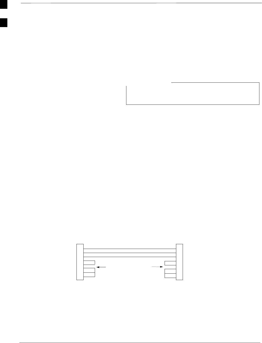
RS–232 to GPIB Interface
SNational Instruments GPIB–232–CT with Motorola CGDSEDN04X
RS232 serial null modem cable or equivalent; used to interface the
LMF to the test equipment.
SStandard RS–232 cable can be used with the following modifications
(see Figure 1-1):
–This solution passes only the 3 minimum electrical connections
between the LMF and the General Purpose Information Bus (GPIB)
interface. The control signals are jumpered as enabled on both ends
of the RS–232 cable (9–pin D). TX and RX signals are crossed as
Null Modem effect. Pin 5 is the ground reference.
–Short pins 7 and 8 together, and short pins 1, 4, and 6 together on
each connector.
Figure 1-1: Null Modem Cable Detail
5
3
2
7
8
1
4
6
GND
RX
TX
RTS
CTS
RSD/DCD
DTR
GND
TX
RX
RTS
CTS
RSD/DCD
DTR
ON BOTH CONNECTORS
SHORT PINS 7, 8;
SHORT PINS 1, 4, & 6
9–PIN D–FEMALE 9–PIN D–FEMALE
5
2
3
7
8
1
4
6
DSR DSR
FW00362
. . . continued on next page
1

Required Test Equipment – continued
Mar 2001 1-9
SCt4812T CDMA BTS Optimization/ATP DRAFT
Model SLN2006A Man Machine Interface (MMI) Interface Kit
SMotorola Model TRN9666A null modem board. Connectors on
opposite sides of the board must be used as this performs a null
modem transformation between cables. This board can be used for
10–pin to 8–pin, 25–pin to 25–pin and 10–pin to 10–pin conversions.
SMotorola 30–09786R01 MMI cable or equivalent; used to interface
the LMF serial port connection to Group Line Interface (GLI2), CSM
and LPA debug serial ports.
S25–pin D to 25–pin D serial cable; used to interface the PC to the null
modem board.
Communications System Analyzer
The communication system analyzer is used during optimization and
testing of the RF communications portion of BTS equipment and
provides the following functions:
(1) Frequency counter
(2) RF power meter (average and code domain)
(3) RF Signal Generator (capable of CDMA modulation)
(4) Spectrum Analyzer
(5) CDMA Code Domain analyzer
Four types of Communication System Analyzer are currently supported
by the LMF. They are:
SHP8921A/600 Analyzer – Including 83203B CDMA Interface,
manual control system card, and 83236A/B Personal communication
Interface (PCS) Interface for 1700/1900 MHz BTS.
SAdvantest R3465 Analyzer – Including R3561L Test Source Unit
SHP8935 Analyzer
SCyberTest Communication Analyzer
GPIB Cables
SHewlett Packard 10833A or equivalent; 1 to 2 meters (3 to 6 feet) long
used to interconnect test equipment and LMF terminal.
Power Meter
One of the following power meters is required with the HP8921 and
Advantest analyzers:
SHewlett Packard Model HP HP437B with HP8481A power sensor
SGigatronics 8541C with model 80601A power sensor
Timing Reference Cables
STwo BNC-male to BNC-male RG316 cables; 3.05 m (10 ft.) long.
Used to connect the communications analyzer to the front timing
reference of the CSM cards in the BTS frame.
Digital Multimeter
SFluke Model 8062A with Y8134 test lead kit or equivalent; used for
precision dc and ac measurements, requiring 4–1/2 digits.
. . . continued on next page
1

Required Test Equipment – continued
DRAFT
SCt4812T CDMA BTS Optimization/ATP Mar 2001
1-10
Directional Coupler
SNarda Model 30661 30 dB (Motorola part no. 58D09732W01)
1900 MHz coupler terminated with two Narda Model 375BN–M
loads, or equivalent.
SNarda Model 30445 30 dB (Motorola Part No. 58D09643T01 )
800 MHz coupler terminated with two Narda Model 375BN–M loads,
or equivalent.
RF Attenuator
S20 dB fixed attenuator, 20 W (Narda 768–20); used with 1.7/1.9 GHz
test cable calibrations or during general troubleshooting procedures.
RF Terminations/Loads
SAt least three 100–Watt (or larger) non–radiating RF
terminations/loads.
Miscellaneous RF Adapters, Loads, etc
SAs required to interface test cables and BTS equipment and for
various test set ups. Should include at least two 50 Ohm loads (type
N) for calibration and one RF short, two N–Type Female–to–Female
Adapters.
LAN Cable
SBNC–to BNC 50 ohm coaxial cable [.91 m (3 ft) maximum] with an
F–to–F adapter, used to connect the 10BaseT–to–coaxial adapter to
the BTS LAN connector.
High–impedance Conductive Wrist Strap
SMotorola Model 42–80385A59; used to prevent damage from
Electrostatic Discharge (ESD) when handling or working with
modules.
Optional Equipment
Not all optional equipment specified here will be supported
by the LMF in automated tests or when executing various
measure type command line interface (CLI) commands. It
is meant to serve as a list of additional equipment that
might be required during maintenance and troubleshooting
operations.
NOTE
Frequency Counter
SStanford Research Systems SR620 or equivalent. If direct
measurement of the 3 MHz or 19.6608 MHz references is required.
. . . continued on next page
1

Required Test Equipment – continued
Mar 2001 1-11
SCt4812T CDMA BTS Optimization/ATP DRAFT
Spectrum Analyzer
SSpectrum Analyzer (HP8594E with CDMA personality card) or
equivalent; required for manual tests.
Local Area Network (LAN) Tester
SModel NETcat 800 LAN troubleshooter (or equivalent); Used to
supplement LAN tests using the ohmmeter.
Span Line (T1/E1) Verification Equipment
SAs required for local application
Oscilloscope
STektronics Model 2445 or equivalent; for waveform viewing, timing,
and measurements or during general troubleshooting procedure.
2–way Splitter
SMini–Circuits Model ZFSC–2–2500 or equivalent; provides the
diversity receive input to the BTS
High Stability 10 MHz Rubidium Standard
SStanford Research Systems SR625 or equivalent – required for CSM
and Low Frequency Receiver/High Stability Oscillator (LFR/HSO)
frequency verification.
Itasca Alarms Test Box
SItasca CGDSCMIS00014 – This test box may be used as a tool to
assist in the testing of customer alarms.
1

Required Documentation
DRAFT
SCt4812T CDMA BTS Optimization/ATP Mar 2001
1-12
Required Documents
The following documents are required to perform optimization of the
cell site equipment:
SSite Document (generated by Motorola Systems Engineering), which
includes:
–General Site Information
–Floor Plan
–RF Power Levels
–Frequency Plan (includes Site PN and Operating Frequencies)
–Channel Allocation (Paging, Traffic, etc.)
–Board Placement
–Site Wiring List
–CDF files (bts–#.cdf and cbsc–#.cdf)
SSC 4812T CDMA BTS Hardware Installation; 68P64113A87
SDemarcation Document (Scope of Work Agreement)
SCDMA LMF Operator’s Guide; 68P64114A78
SCDMA RFDS Hardware Installation manual; 68P64113A93
SCDMA RFDS User’s Guide, 68P64113A37
SLMF CLI Commands, R15.x, 68P09251A59
SEquipment Manuals for non-Motorola test equipment
Intended Reader Profile
The information in this manual set is intended for use by the cellular
communications craftsperson(s) in the initial installation and
configuration, as well as the day-to-day operation and maintenance of a
BTS.
The user of this information has a general understanding of telephony, as
used in the operation of the Public Switched Telephone
Network (PSTN), and is familiar with these concepts as they are applied
in the cellular and maintenance mobile/portable radiotelephone
environment.
The user also needs a working knowledge of the computer platform
operating system being used (for example, Windows 95 or
Windows 98).
1

BTS Equipment Identification
Mar 2001 1-13
SCt4812T CDMA BTS Optimization/ATP DRAFT
Equipment Overview
The Motorola SC 4812T BTS can consist of the following equipment
frames:
SAt least one BTS starter frame
–+27 V BTS (see Figure 1-2)
––48 V BTS (see Figure 1-3)
SAncillary equipment frame (or wall mounted equipment)
SExpansion frames
–+27 V BTS (see Figure 1-4)
––48 V BTS (see Figure 1-5)
Ancillary Equipment Frame
Identification
Equipment listed below can be wall mounted or mounted
in a standard 19 inch frame. The description assumes that
all equipment is mounted in a frame for clarity.
NOTE
If equipped with the RFDS option, the RFDS and directional couplers
are the interface between the site antennas and the BTS or Modem
frame. The RFDS equipment includes:
SDirectional couplers
SSite receive bandpass/bandreject filters
SRFDS
Logical BTS
The BTS software implements the logical BTS capability. Previously, all
BTS frames co–located at a single site had to be identified in the
network with separate and distinct BTS ID numbers. In the Logical BTS
feature, all frames located at a single BTS site are identified with unique
Frame ID numbers (Frame ID Numbers 1, 101, 201, 301) under a single
(site) BTS ID number. A logical BTS can consist of up to four
SC 4812T frames.When the LMF is connected to frame 1 of a logical
BTS, you can access all devices in all of the frames that make up the
logical BTS. A logical BTS requires a CDF file that includes equipage
information for all of the logical BTS frames and their devices and a
CBSC file that includes channel data for all of the logical BTS fames.
. . . continued on next page
1
BTS Equipment Identification – continued
DRAFT
SCt4812T CDMA BTS Optimization/ATP Mar 2001
1-14
Logical BTS Numbering
The first frame of a logical BTS has a –1 suffix (e.g., BTS–812–1).
Other frames of the logical BTS are numbered with suffixes, –101, –201,
and –301 (e. g. BTS–812–201). When you log into a BTS, a FRAME
tab is displayed for each frame. If there is only one frame for the BTS,
there is only one tab (e.g., FRAME–282–1) for BTS–282. If a logical
BTS has more than one frame, there is a separate FRAME tab for each
frame (e.g. FRAME–438–1, FRAME–438–101, and FRAME–438–201
for a BTS–438 that has three frames). If an RFDS is included in the
CDF file, an RFDS tab (e.g., RFDS–438–1) is displayed.
Actions (e.g., ATP tests) can be initiated for selected devices in one or
more frames of a logical BTS. Refer to the Select devices help screen for
information on how to select devices.
C–CCP Shelf Card/Module Device ID Numbers
All cards/modules/boards in the frames at a single site, assigned to a
single BTS number, are also identified with unique Device ID numbers
dependent upon the Frame ID number in which they are located. Refer to
Table 1-1 and Table 1-2 for specific C–CCP Shelf Device ID numbers.
Table 1-1: C–CCP Shelf/Cage Card/Module Device ID Numbers (Top Shelf)
Frame Card/Module ID Number (Left to Right)
#Power
(PS–1) Power
(PS–2) Power
(PS–3) AMR
–1 GLI2
–1 MCC BBX BBX–
RMPC/
EMPC
–1
1–––1 1123456123456 R1 –
101 –––101 101 101 102 103 104 105 106 101 102 103 104 105 106 R101 –
201 –––201 201 201 202 203 204 205 206 201 202 203 204 205 206 R201 –
301 –––301 301 301 302 303 304 305 306 301 302 303 304 305 306 R301 –
Table 1-2: C–CCP Shelf/Cage Card/Module Device ID Numbers (Bottom Shelf)
Frame Card/Module ID Number (Left to Right)
#HSO/
LFR CSM
–1 CSM
–2 CCD
ACCD
BAMR
–2 GLI2–
2MCC BBX SW MPC/
EMPC
–2
1–1 2 – – – 2 2 7 8 9 10 11 12 7 8 9 10 11 12 – –
101 –101 102 – – – 102 102 107 108 109 110 111 112 107 108 109 110 111 112 – –
201 –201 202 – – – 202 102 207 208 209 210 211 212 207 208 209 210 211 212 – –
301 –301 302 – – – 302 102 307 308 309 310 311 312 307 308 309 310 311 312 – –
1
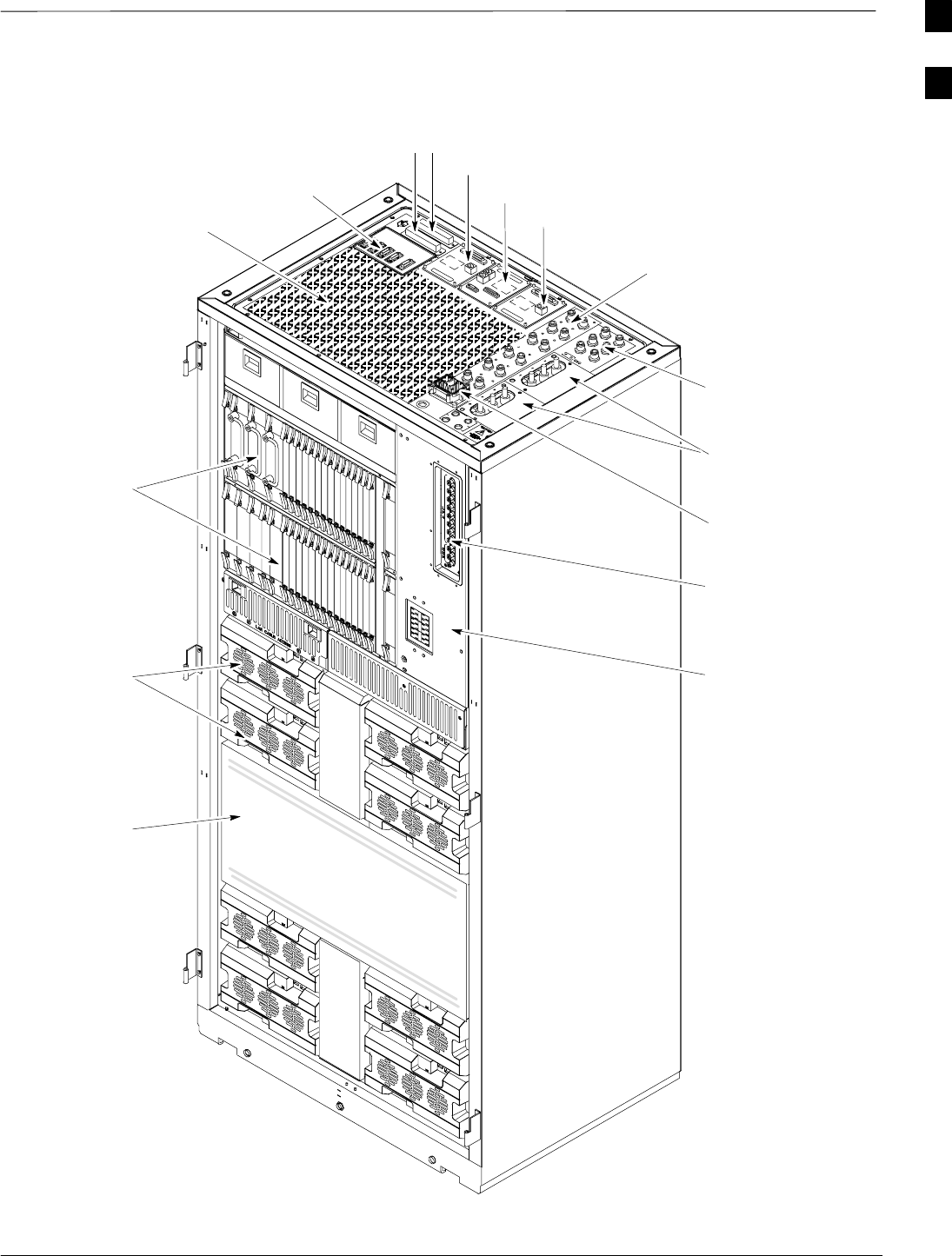
BTS Equipment Identification – continued
Mar 2001 1-15
SCt4812T CDMA BTS Optimization/ATP DRAFT
Expansion I/O
Housing
For clarity, doors are not shown. FW00214
Front Cosmetic
Panel
Power Input
Connection
TX Out (1 – 6)
Span I/O B
Span I/O A
Site I/O
RX In (1A – 6A
and 1B – 6B)
Exhaust Region
C–CCP Cage
Breakers
Combiner
Section
RGD (Needed for
Expansion only)
LPA Cage
Alarm
Connectors
Figure 1-2: +27 V SC 4812T BTS Starter Frame
1
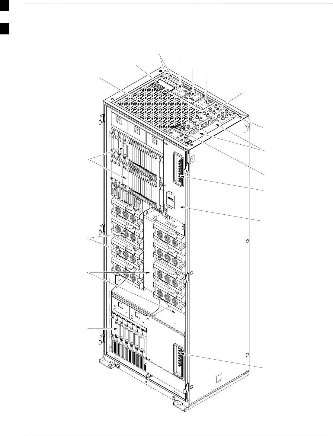
BTS Equipment Identification – continued
DRAFT
SCt4812T CDMA BTS Optimization/ATP Mar 2001
1-16
Figure 1-3: –48 V SC 4812T BTS Starter Frame
FW00477
Expansion I/O
Housing
For clarity, doors are not shown.
Front Cosmetic
Panel
Power Input
Connection
TX Out (1 – 6)
Span I/O B
Span I/O A
Site I/O
RX In (1A – 6A
and 1B – 6B)
Exhaust Region
C–CCP Cage
Breakers
Combiner
Section
RGD (Needed for
Expansion only)
LPA Cage
Power
Conversion
Shelf
Breakers
Alarms
1

BTS Equipment Identification – continued
Mar 2001 1-17
SCt4812T CDMA BTS Optimization/ATP DRAFT
Figure 1-4: +27 V SC 4812T BTS Expansion Frame
Power Input
Connection
TX Out (1 – 6)
Span I/O B
Span I/O A
Site I/O
Expansion Port
to another BTS
Exhaust Region
C–CCP Cage
Breakers
LPA Cage
For clarity, doors are not shown.
FW00093
LAN
Combiner
Section
1
BTS Equipment Identification – continued
DRAFT
SCt4812T CDMA BTS Optimization/ATP Mar 2001
1-18
Figure 1-5: –48 V SC 4812T BTS Expansion Frame
FW00478
Expansion Port
to another BTS
For clarity, doors are not shown.
Power Input
Connection
TX Out (1 – 6)
Span I/O B
Span I/O A
Site I/O
Exhaust Region
C–CCP Cage
Breakers
Combiner
Section
LPA Cage
Power
Conversion
Shelf
LAN
Breakers
Alarms
1

BTS Equipment Identification – continued
Mar 2001 1-19
SCt4812T CDMA BTS Optimization/ATP DRAFT
BTS Frame Description
The BTS is the interface between the span lines to/from the Cellsite Base
Station Controller (CBSC) and the site antennas. This frame is described
in three sections:
SThe top interconnect plate where all connections are made.
SThe upper portion of the frame which houses circuit breakers, cooling
fans, and the C–CCP shelf.
SThe lower portion of the frame which houses the LPA fans, LPAs, and
TX filter/combiners.
SThe –48 V version of the BTS also has a section below the LPAs
containing a power conversion shelf that supplies power to the LPAs.
Use the illustrations that follow to visually identify the major
components, that make up the Motorola SC 4812T BTS frame.
Top Interconnect Plate (see Figure 1-6 or Figure 1-7)
All cabling to and from the BTS equipment frames is via the
interconnect panel on the top of each frame. Connections made here
include:
SSpan lines
SRX antennas
STX antenna
SAlarm connections
SPower input
SLAN connections
SGPS input or Remote Global Positioning System (RGPS) on the Site
I/O Board
SRemote Global Positioing System Distribution (RGD)
SLORAN–C Low Frequency Receiver (LFR) input
SExpansion frame connection
SGround connections
C–CCP Shelf (see Figure 1-10)
SC–CCP backplane and cage
SPower supply modules
SCDMA clock distribution (CCD) boards
SCSM and HSO/LFR boards
SAlarm Monitoring and Reporting (AMR) boards
SGLI2 cards
SMPC boards (starter frame only)
SEMPC boards (expansion frames)
. . . continued on next page
1

BTS Equipment Identification – continued
DRAFT
SCt4812T CDMA BTS Optimization/ATP Mar 2001
1-20
SSwitch card
SMCC boards (may be MCC8E, MCC24, or MCC–1X)
SBBX boards (may be BBX2 or BBX–1X)
SCIO boards
PA Shelves (see Figure 1-11 or Figure 1-12)
SLPA cages
SLPA trunking backplanes
SSingle Tone Linear Power Amplifier (STLPA, or more commonly
referred to as “LPA”) modules
SLPA fan modules
SLPA Combiner Cage (+27 V BTS)
STX filter combiners or bandpass filters
–48 V Power Conversion Shelf (see Figure 1-15)
SPower conversion backplane and shelf
SPower conversion boards
SPower conversion alarm card
SFan modules
SPower distribution assembly
SAir plenum
1
Frame Module Location & Identification
Mar 2001 1-21
SCt4812T CDMA BTS Optimization/ATP DRAFT
Figure 1-6: +27 V SC 4812T Starter Frame I/O Plate
ALARM
CONNECTORS
OUT
LAN
IN
LAN
GPS
AB
AB
SPAN I/O A SITE I/O SPAN I/O B
LFR/
ALARM B 4
3A
2A
1A
6A
5A
4A
3B
2B
1B
6B
5B
4B
GND
5
6
1
2
3
TX OUT
SPAN I/O ASPAN I/O B
CAUTION
LIVE TERMINALSLIVE TERMINALS +27 VDC
HSO
RX
ALARM A
EXP I/O
RGD
LOW FREQUENCY
RECEIVER / HSO
FRONT
REAR
SPAN I/O
RF EXPANSION PORT
(TO ANOTHER BTS)
TRANSMIT
ANTENNA
CONNECTORS
POWER INPUT
RECEIVE ANTENNA
CONNECTORS
SITE I/OSPAN I/O
FW00215
GPS IN LAN CONNECTIONS
RGPS
REF
1

Frame Module Location & Identification – continued
DRAFT
SCt4812T CDMA BTS Optimization/ATP Mar 2001
1-22
Figure 1-7: –48 V SC 4812T Starter Frame I/O Plate
OUT
LAN
IN
LAN
GPS
AB
AB
SPAN I/O A SITE I/O SPAN I/O B
LFR
ALARM B 4
3A
2A
1A
6A
5A
4A
3B
2B
1B
6B
5B
4B
GND
5
6
1
2
3
TX OUT
SPAN I/O ASPAN I/O B
CAUTION
LIVE TERMINALSLIVE TERMINALS WIRED FOR –48VDC
HSO/
RX
ALARM A
EXP I/O
RGD
HSO/LFR
FRONT
REAR
SPAN I/O
RF EXPANSION
PORT (TO
ANOTHER BTS)
TRANSMIT
ANTENNA
CONNECTORS
POWER INPUT
RECEIVE ANTENNA
CONNECTORS
SPAN I/O
FW00479
SITE I/O
ALARM
CONNECTORS
RX
3
2
1
1
2
3
AB
LAN
CONNECTIONS
GPS IN
SITE I/O
RGPS
REF
1
Frame Module Location & Identification – continued
Mar 2001 1-23
SCt4812T CDMA BTS Optimization/ATP DRAFT
Figure 1-8: +27 V SC 4812T Expansion Frame I/O Plate
OUT
LAN
IN
LAN
AB
AB
GPS
EXP IN
SPAN I/O A SITE I/O SPAN I/O B
LFR/
ALARM B
4
GND
5
6
1
2
3
TX OUT
FRONT
REAR
SPAN I/O ASPAN I/O B
AB
CAUTION
LIVE TERMINALSLIVE TERMINALS +27 VDC
HSO
EXP OUT
AB
ALARM A
FW00082
EXP IN
HOUSING
TRANSMIT
ANTENNA
CONNECTORS
EXP OUT
HOUSING (ADDED
ONLY WHEN
USING SECOND
EXPANSION
FRAME)
SITE I/O LFR/HSO
RGD
POWER
INPUT
LAN
SPAN I/O SPAN I/O
RGPS
REF
1
Frame Module Location & Identification – continued
DRAFT
SCt4812T CDMA BTS Optimization/ATP Mar 2001
1-24
Figure 1-9: –48 V SC 4812T Expansion Frame I/O Plate
OUT
LAN
IN
LAN
AB
AB
GPS
EXP IN
SPAN I/O A SITE I/O SPAN I/O B
LFR
ALARM B
4
GND
5
6
1
2
3
TX OUT
FRONT
REAR
SPAN I/O ASPAN I/O B
AB
CAUTION
LIVE TERMINALS
HSO/
EXP OUT
AB
ALARM A
FW00480
EXP IN
HOUSING
TRANSMIT
ANTENNA
CONNECTORS
EXP OUT
HOUSING (ADDED
ONLY WHEN
USING SECOND
EXPANSION
FRAME)
SITE I/O
RGD
POWER
INPUT
LAN
SPAN I/O SPAN I/O
1
2
3
1
2
3
LIVE TERMINALS WIRED FOR –48 VDC
SITE I/O
HSO/LFR
RF FILTER PORTS NOT USED
IN EXPANSION FRAME
RGPS
REF
1
Frame Module Location & Identification – continued
Mar 2001 1-25
SCt4812T CDMA BTS Optimization/ATP DRAFT
Figure 1-10: SC 4812T C–CCP Shelf
19 mm Filler Panel
PS–3
AMR–1
CSM–1
CSM–2
38 mm Filler Panel
AMR–2
GLI2–1GLI2–2
MCC24–6
BBX2–1
BBX2–2
BBX2–3
BBX2–4
BBX2–5
BBX2–6
BBX2–RSwitch
MPC/EMPC–1MPC/EMPC–2
CIO
BBX2–7
BBX2–8
BBX2–9
BBX2–10
BBX2–11
BBX2–12
MCC24–5
MCC24–4
MCC24–3
MCC24–2
MCC24–1
MCC24–12
MCC24–11
MCC24–10
MCC24–9
MCC24–8
MCC24–7
PS–2
PS–1
CCD–2 CCD–1
NOTE: MCCs may be
MCC8Es, MCC24s, or
MCC–1Xs. BBXs may
be BBX2s or BBX–1Xs.
HSO/LFR
FW00295
REF
1
Frame Module Location & Identification – continued
DRAFT
SCt4812T CDMA BTS Optimization/ATP Mar 2001
1-26
LPA1A
LPA1B
LPA1C
LPA1D
LPA3A
LPA3B
LPA3C
LPA3D
LPA2A
LPA2B
LPA2C
LPA2D
LPA4A
LPA4B
LPA4C
LPA4D
FAN
MODULE
(TYPICAL)
FILTERS /
COMBINERS
(2 TO 1 COMBINER
SHOWN)
Note
No adjacent carriers may exist within the same TX filter
combiner. “Adjacent” is defined as fc1 and fc2 being
1.25 MHz apart (center–to–center). “Non–adjacent” is
defined as fc1 and fc2 being >2.50 MHz apart
(center–to–center).
123
456
4–CARRIER CONFIGURATION
CARRIER
1
3
CARRIER
2
4
123
456
FW00296
Figure 1-11: +27 V SC 4812T LPA Configuration – 4 Carrier with 2:1 Combiners
1

Frame Module Location & Identification – continued
Mar 2001 1-27
SCt4812T CDMA BTS Optimization/ATP DRAFT
Figure 1-12: –48 V SC 4812T LPA Configuration – 4 Carrier, 3–Sector with 2:1 Combiners
LPA1A
LPA1B
Note
No adjacent carriers may exist within the same TX filter
combiner. “Adjacent” is defined as fc1 and fc2 being
1.25 MHz apart (center–to–center). “Non–adjacent” is
defined as fc1 and fc2 being >2.50 MHz apart
(center–to–center).
4–CARRIER CONFIGURATION
CARRIER CARRIER
LPA1C
LPA1D
LPA3C
LPA3D
LPA2A
LPA2B
LPA2C
LPA2D
LPA4C
LPA4D
FW00481
1
2
3
4
5
6
12
3 4
1
2
3
4
5
6
LPA3A
LPA3B
LPA4A
LPA4B
FAN
MODULE
(TYPICAL)
FILTERS /
COMBINERS
(2 TO 1 COMBINER
SHOWN)
–48 Volt
SC 4812T
1
Frame Module Location & Identification – continued
DRAFT
SCt4812T CDMA BTS Optimization/ATP Mar 2001
1-28
Sector Configuration
There are a number of ways to configure the BTS frame. Table 1-3
outlines the basic requirements. When carrier capacity is greater than
two, a 2:1 or 4:1 cavity combiner must be used. For one or two carriers,
bandpass filters or cavity combiners may be used, depending on
sectorization and channel sequencing.
Table 1-3: BTS Sector Configuration
Number
of carriers Number
of sectors Channel
spacing Filter requirements
13 or 6 N/A Bandpass Filter, Cavity Combiner
(2:1 or 4:1)
2 6 Non–adjacent Cavity Combiner (2:1 Only)
2 6 Adjacent Not supported in single frame
2 3 Non–adjacent Cavity Combiner (2:1 or 4:1)
2 3 Adjacent Bandpass Filter
3,4 3 Non–adjacent Cavity Combiner (2:1 or 4:1)
3,4 3 Adjacent Cavity Combiner (2:1 Only)
In Table 1-4, BBXs may be BBX2s or BBX–1Xs.
NOTE
1
Frame Module Location & Identification – continued
Mar 2001 1-29
SCt4812T CDMA BTS Optimization/ATP DRAFT
Table 1-4: Sector Configurations
Config Ref. No. Description
3–Sector/2–ADJACENT Carriers – The configuration below maps TX with optional 2:1 cavity
combiners for 3 sectors/2 carriers for adjacent channels. Note that 2:1 cavity combiners are used (6
total).
1TX1 TX2 TX3 TX4 TX5 TX6 Carrier#
BBX–1 BBX–2 BBX–3 N/A N/A N/A 1
N/A N/A N/A BBX–4 BBX–5 BBX–6 2
6–Sector/2–NON–ADJACENT Carriers – The configuration below maps TX with 2:1 cavity
combiners for 6 sectors/2 carriers for non–adjacent channels.
2TX1 TX2 TX3 TX4 TX5 TX6 Carrier#
BBX–1 BBX–2 BBX–3 BBX–4 BBX–5 BBX–6 1
BBX–7 BBX–8 BBX–9 BBX–10 BBX–11 BBX–12 2
3–Sector/2–NON–ADJACENT Carriers – The configuration below maps TX with 2:1 cavity
combiners for 3 sectors/2 carriers for non–adjacent channels.
3TX1 TX2 TX3 TX4 TX5 TX6 Carrier#
BBX–1 BBX–2 BBX–3 N/A N/A N/A 1
BBX–7 BBX–8 BBX–9 N/A N/A N/A 2
3–Sector/4–ADJACENT Carriers – The configuration below maps TX with 2:1 cavity combiners
for 3 sector/4 carriers for adjacent channels.
TX1 TX2 TX3 TX4 TX5 TX6 Carrier#
4BBX–1 BBX–2 BBX–3 N/A N/A N/A 1
BBX–7 BBX–8 BBX–9 N/A N/A N/A 2
N/A N/A N/A BBX–4 BBX–5 BBX–6 3
N/A N/A N/A BBX–10 BBX–11 BBX–12 4
3–Sector / 2–ADJACENT Carriers – The configuration below maps TX with bandpass filters for
3 sectors/2 carriers for adjacent channels.
5TX1 TX2 TX3 TX4 TX5 TX6 Carrier#
BBX–1 BBX–2 BBX–3 N/A N/A N/A 1
N/A N/A N/A BBX–7 BBX–8 BBX–9 2
3–Sector/3 or 4–NON–ADJACENT Carriers – The configuration below maps TX with 4:1
cavity combiners for 3 sectors/3 or 4 carriers for non–adjacent channels.
TX1 TX2 TX3 TX4 TX5 TX6 Carrier#
6BBX–1 BBX–2 BBX–3 N/A N/A N/A 1
BBX–7 BBX–8 BBX–9 N/A N/A N/A 2
BBX–4 BBX–5 BBX–6 N/A N/A N/A 3
BBX–10 BBX–11 BBX–12 N/A N/A N/A 4
6–Sector/1–Carrier – The configuration below maps TX with either bandpass filters or 2:1 cavity
combiners for 6 sector/1 carrier.
7TX1 TX2 TX3 TX4 TX5 TX6 Carrier#
BBX–1 BBX–2 BBX–3 BBX–4 BBX–5 BBX–6 1
1
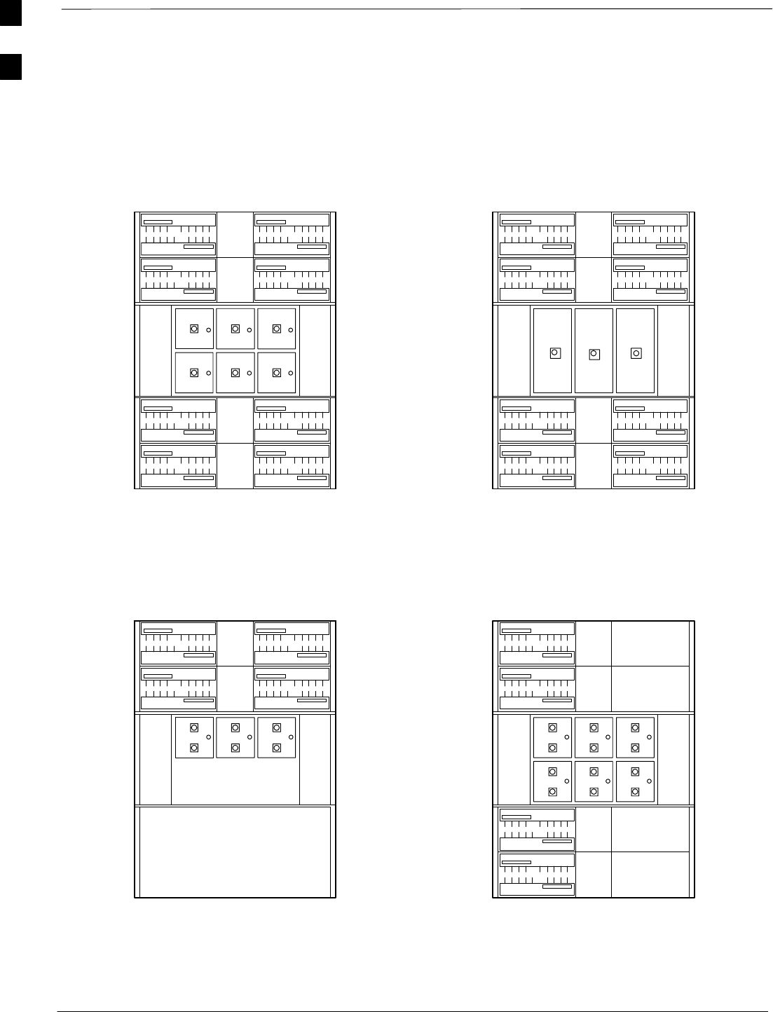
Frame Module Location & Identification – continued
DRAFT
SCt4812T CDMA BTS Optimization/ATP Mar 2001
1-30
Numbering
456
LPA 1A
LPA 1B
LPA 1C
LPA 1D
LPA 3C
LPA 3A
LPA 3B
LPA 3D
LPA 2D
LPA 2C
LPA 2B
LPA 2A
LPA 4B
LPA 4A
LPA 4C
LPA 4D
Sector
3 Sector
Sector
3 Sector
(6 Sector)
Numbering
2 to 1 Combiner
3 Sector or 6 Sector
C1, S1–3
(C1, S1–3) C2, S1–3
(C2, S1–3)
C3, S1–3
(C1, S4–6) C4, S1–3
(C2, S4–6)
(6 Sector)
123
456
LPA 1A
LPA 1B
LPA 1C
LPA 1D
LPA 3C
LPA 3A
LPA 3B
LPA 3D
LPA 2D
LPA 2C
LPA 2B
LPA 2A
LPA 4B
LPA 4A
LPA 4C
LPA 4D
Sector
Numbering Sector
Numbering
4 to 1 Combiner
3 Sector
C1, S1–3 C2, S1–3
C3, S1–3 C4, S1–3
123
LPA 1A
LPA 1B
LPA 1C
LPA 1D LPA 2D
LPA 2C
LPA 2B
LPA 2A
Sector
3 Sector
Numbering Sector
3 Sector
Numbering
Dual Bandpass Filter
3 Sector Only
C1, S1–3 C2, S1–3
123
456
LPA 1A
LPA 1B
LPA 1C
LPA 1D
LPA 3C
LPA 3A
LPA 3B
LPA 3D
Sector
Numbering Dual Bandpass Filter
6 Sector
C1, S1–3
C1, S4–6
2 Carrier Maximum 1 Carrier Only
6 Sector
123
Figure 1-13: +27 V SC4812T LPA Configuration with Combiners/Filters
Note: See Table 1-4 Configuration
Reference Numbers 1, 2, 3, 4. Note: See Table 1-4 Configuration
Reference Number 6.
Note: See Table 1-4 Configuration
Reference Number 5. Note: See Table 1-4 Configuration
Reference Number 7.
FW00297
1
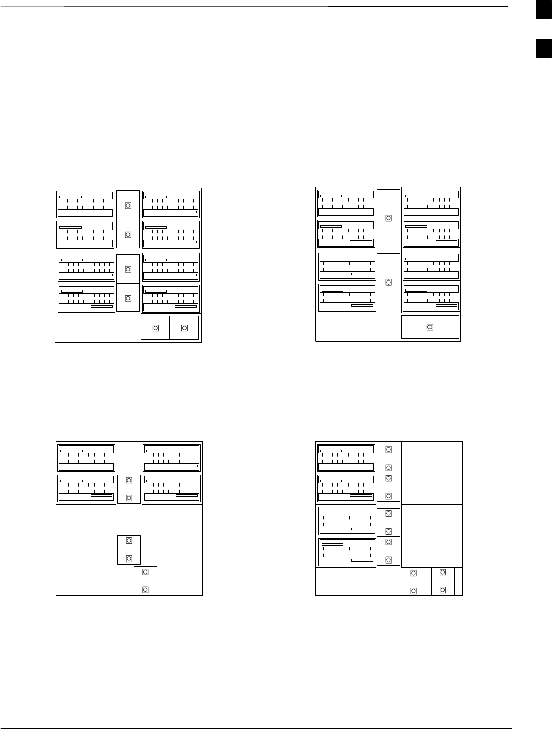
Frame Module Location & Identification – continued
Mar 2001 1-31
SCt4812T CDMA BTS Optimization/ATP DRAFT
Figure 1-14: –48 V SC4812T LPA Configuration with Combiners/Filters
Note: See Table 1-4 Configuration
Reference Numbers 1, 2, 3, 4. Note: See Table 1-4 Configuration
Reference Number 6.
Note: See Table 1-4 Configuration
Reference Number 5. Note: See Table 1-4 Configuration
Reference Number 7.
REF FW00482
4
1
5
2
36
Numbering
Sector
3 Sector
Sector
3 Sector
(6 Sector)
Numbering
2 to 1 Combiner
3 Sector or 6 Sector
C1, S1–3
(C1, S1–3) C2, S1–3
(C2, S1–3)
C3, S1–3
(C1, S4–6) C4, S1–3
(C2, S4–6)
(6 Sector)
LPA 1A
LPA 1B
LPA 1C
LPA 1D
LPA 3C
LPA 3A
LPA 3B
LPA 3D
LPA 2D
LPA 2C
LPA 2B
LPA 2A
LPA 4B
LPA 4A
LPA 4C
LPA 4D
Sector
Numbering Sector
Numbering
4 to 1 Combiner
3 Sector
C1, S1–3 C2, S1–3
C3, S1–3 C4, S1–3
LPA 1A
LPA 1B 1
3
LPA 1C
LPA 1D
LPA 3C
LPA 3A
LPA 3B
LPA 3D
LPA 2D
LPA 2C
LPA 2B
LPA 2A
LPA 4B
LPA 4A
LPA 4C
LPA 4D
2
LPA 1A
LPA 1B
LPA 1C
LPA 1D LPA 2D
LPA 2C
LPA 2B
LPA 2A
4
5
Sector
3 Sector
Numbering Sector
3 Sector
Numbering
Dual Bandpass Filter
3 Sector Only
C1, S1–3 C2, S1–3
2 Carrier Maximum
2
1
3
6
1
5
2
4
LPA 1A
LPA 1B
LPA 1C
LPA 1D
LPA 3C
LPA 3A
LPA 3B
LPA 3D
Sector
Numbering
Dual Bandpass Filter
6 Sector
C1, S1–3
C1, S4–6
1 Carrier Only
6 Sector
3 Sector
3 Sector
36
1
Frame Module Location & Identification – continued
DRAFT
SCt4812T CDMA BTS Optimization/ATP Mar 2001
1-32
Figure 1-15: –48 V BTS Power Conversion Shelf
FW00501
PS–6
AMR
PS–5
PS–4
PS–9
PS–8
PS–7
1C
1A
2A
2C
3C
3A
4A
4C
L
P
A
1D
1B
2B
2D
3D
3B
4B
4D
30
30
30
30
30
30
30
30
FAN
MODULE
PWR/ALM
REAR
FRONT
FAN
MODULE
PWR/ALM
REAR
FRONT
1
Frame Module Location & Identification – continued
Mar 2001 1-33
SCt4812T CDMA BTS Optimization/ATP DRAFT
Figure 1-16: CDMA (COBRA) RFDS Layout
AMR–B
(RS–485 SERIAL)
AMR–A
(RS–485 SERIAL)
Cobra RFDS external housing
(Shown With Cover off)
POWER SUPPLY
ON/OFF ROCKER
SWITCH
MMI PORT AND
PWR/ALARM LED
Cobra RFDS Field Replaceable Unit (FRU)
(shown removed from external housing)
CHASSIS GND
POWER
CONNECTOR
Cobra RFDS RF connector
panel detail
(shown from rear)
ELECTRICAL GND
FRONT VIEW
CASU 1
CASU 2
FWTIC
SUA ESN LABEL
(FOR SC XXXX SERIES BTS)
MMI
LEDS
ESN LABEL
(FOR SC 6XX SERIES BTS)
FW00138
1

Frame Module Location & Identification – continued
DRAFT
SCt4812T CDMA BTS Optimization/ATP Mar 2001
1-34
Notes
1